CN100416768C - Wafer coating and singulation method - Google Patents
Wafer coating and singulation method Download PDFInfo
- Publication number
- CN100416768C CN100416768C CNB038214520A CN03821452A CN100416768C CN 100416768 C CN100416768 C CN 100416768C CN B038214520 A CNB038214520 A CN B038214520A CN 03821452 A CN03821452 A CN 03821452A CN 100416768 C CN100416768 C CN 100416768C
- Authority
- CN
- China
- Prior art keywords
- wafer
- chip
- integrated circuit
- groove
- filler
- Prior art date
- Legal status (The legal status is an assumption and is not a legal conclusion. Google has not performed a legal analysis and makes no representation as to the accuracy of the status listed.)
- Expired - Fee Related
Links
Images


Classifications
-
- H—ELECTRICITY
- H01—ELECTRIC ELEMENTS
- H01L—SEMICONDUCTOR DEVICES NOT COVERED BY CLASS H10
- H01L21/00—Processes or apparatus adapted for the manufacture or treatment of semiconductor or solid state devices or of parts thereof
- H01L21/02—Manufacture or treatment of semiconductor devices or of parts thereof
- H01L21/04—Manufacture or treatment of semiconductor devices or of parts thereof the devices having at least one potential-jump barrier or surface barrier, e.g. PN junction, depletion layer or carrier concentration layer
- H01L21/50—Assembly of semiconductor devices using processes or apparatus not provided for in a single one of the subgroups H01L21/06 - H01L21/326, e.g. sealing of a cap to a base of a container
- H01L21/56—Encapsulations, e.g. encapsulation layers, coatings
- H01L21/561—Batch processing
-
- H—ELECTRICITY
- H01—ELECTRIC ELEMENTS
- H01L—SEMICONDUCTOR DEVICES NOT COVERED BY CLASS H10
- H01L21/00—Processes or apparatus adapted for the manufacture or treatment of semiconductor or solid state devices or of parts thereof
- H01L21/02—Manufacture or treatment of semiconductor devices or of parts thereof
- H01L21/04—Manufacture or treatment of semiconductor devices or of parts thereof the devices having at least one potential-jump barrier or surface barrier, e.g. PN junction, depletion layer or carrier concentration layer
- H01L21/50—Assembly of semiconductor devices using processes or apparatus not provided for in a single one of the subgroups H01L21/06 - H01L21/326, e.g. sealing of a cap to a base of a container
- H01L21/56—Encapsulations, e.g. encapsulation layers, coatings
- H01L21/563—Encapsulation of active face of flip-chip device, e.g. underfilling or underencapsulation of flip-chip, encapsulation preform on chip or mounting substrate
-
- H—ELECTRICITY
- H01—ELECTRIC ELEMENTS
- H01L—SEMICONDUCTOR DEVICES NOT COVERED BY CLASS H10
- H01L21/00—Processes or apparatus adapted for the manufacture or treatment of semiconductor or solid state devices or of parts thereof
- H01L21/70—Manufacture or treatment of devices consisting of a plurality of solid state components formed in or on a common substrate or of parts thereof; Manufacture of integrated circuit devices or of parts thereof
- H01L21/77—Manufacture or treatment of devices consisting of a plurality of solid state components or integrated circuits formed in, or on, a common substrate
- H01L21/78—Manufacture or treatment of devices consisting of a plurality of solid state components or integrated circuits formed in, or on, a common substrate with subsequent division of the substrate into plural individual devices
-
- H—ELECTRICITY
- H01—ELECTRIC ELEMENTS
- H01L—SEMICONDUCTOR DEVICES NOT COVERED BY CLASS H10
- H01L23/00—Details of semiconductor or other solid state devices
- H01L23/28—Encapsulations, e.g. encapsulating layers, coatings, e.g. for protection
- H01L23/31—Encapsulations, e.g. encapsulating layers, coatings, e.g. for protection characterised by the arrangement or shape
- H01L23/3107—Encapsulations, e.g. encapsulating layers, coatings, e.g. for protection characterised by the arrangement or shape the device being completely enclosed
- H01L23/3114—Encapsulations, e.g. encapsulating layers, coatings, e.g. for protection characterised by the arrangement or shape the device being completely enclosed the device being a chip scale package, e.g. CSP
-
- H—ELECTRICITY
- H01—ELECTRIC ELEMENTS
- H01L—SEMICONDUCTOR DEVICES NOT COVERED BY CLASS H10
- H01L24/00—Arrangements for connecting or disconnecting semiconductor or solid-state bodies; Methods or apparatus related thereto
- H01L24/01—Means for bonding being attached to, or being formed on, the surface to be connected, e.g. chip-to-package, die-attach, "first-level" interconnects; Manufacturing methods related thereto
- H01L24/26—Layer connectors, e.g. plate connectors, solder or adhesive layers; Manufacturing methods related thereto
- H01L24/28—Structure, shape, material or disposition of the layer connectors prior to the connecting process
- H01L24/29—Structure, shape, material or disposition of the layer connectors prior to the connecting process of an individual layer connector
-
- H—ELECTRICITY
- H01—ELECTRIC ELEMENTS
- H01L—SEMICONDUCTOR DEVICES NOT COVERED BY CLASS H10
- H01L24/00—Arrangements for connecting or disconnecting semiconductor or solid-state bodies; Methods or apparatus related thereto
- H01L24/93—Batch processes
- H01L24/95—Batch processes at chip-level, i.e. with connecting carried out on a plurality of singulated devices, i.e. on diced chips
- H01L24/96—Batch processes at chip-level, i.e. with connecting carried out on a plurality of singulated devices, i.e. on diced chips the devices being encapsulated in a common layer, e.g. neo-wafer or pseudo-wafer, said common layer being separable into individual assemblies after connecting
-
- H—ELECTRICITY
- H01—ELECTRIC ELEMENTS
- H01L—SEMICONDUCTOR DEVICES NOT COVERED BY CLASS H10
- H01L24/00—Arrangements for connecting or disconnecting semiconductor or solid-state bodies; Methods or apparatus related thereto
- H01L24/93—Batch processes
- H01L24/95—Batch processes at chip-level, i.e. with connecting carried out on a plurality of singulated devices, i.e. on diced chips
- H01L24/97—Batch processes at chip-level, i.e. with connecting carried out on a plurality of singulated devices, i.e. on diced chips the devices being connected to a common substrate, e.g. interposer, said common substrate being separable into individual assemblies after connecting
-
- H—ELECTRICITY
- H01—ELECTRIC ELEMENTS
- H01L—SEMICONDUCTOR DEVICES NOT COVERED BY CLASS H10
- H01L21/00—Processes or apparatus adapted for the manufacture or treatment of semiconductor or solid state devices or of parts thereof
- H01L21/02—Manufacture or treatment of semiconductor devices or of parts thereof
- H01L21/04—Manufacture or treatment of semiconductor devices or of parts thereof the devices having at least one potential-jump barrier or surface barrier, e.g. PN junction, depletion layer or carrier concentration layer
- H01L21/18—Manufacture or treatment of semiconductor devices or of parts thereof the devices having at least one potential-jump barrier or surface barrier, e.g. PN junction, depletion layer or carrier concentration layer the devices having semiconductor bodies comprising elements of Group IV of the Periodic System or AIIIBV compounds with or without impurities, e.g. doping materials
- H01L21/30—Treatment of semiconductor bodies using processes or apparatus not provided for in groups H01L21/20 - H01L21/26
- H01L21/302—Treatment of semiconductor bodies using processes or apparatus not provided for in groups H01L21/20 - H01L21/26 to change their surface-physical characteristics or shape, e.g. etching, polishing, cutting
- H01L21/304—Mechanical treatment, e.g. grinding, polishing, cutting
- H01L21/3043—Making grooves, e.g. cutting
-
- H—ELECTRICITY
- H01—ELECTRIC ELEMENTS
- H01L—SEMICONDUCTOR DEVICES NOT COVERED BY CLASS H10
- H01L2224/00—Indexing scheme for arrangements for connecting or disconnecting semiconductor or solid-state bodies and methods related thereto as covered by H01L24/00
- H01L2224/01—Means for bonding being attached to, or being formed on, the surface to be connected, e.g. chip-to-package, die-attach, "first-level" interconnects; Manufacturing methods related thereto
- H01L2224/10—Bump connectors; Manufacturing methods related thereto
- H01L2224/15—Structure, shape, material or disposition of the bump connectors after the connecting process
- H01L2224/16—Structure, shape, material or disposition of the bump connectors after the connecting process of an individual bump connector
-
- H—ELECTRICITY
- H01—ELECTRIC ELEMENTS
- H01L—SEMICONDUCTOR DEVICES NOT COVERED BY CLASS H10
- H01L2224/00—Indexing scheme for arrangements for connecting or disconnecting semiconductor or solid-state bodies and methods related thereto as covered by H01L24/00
- H01L2224/01—Means for bonding being attached to, or being formed on, the surface to be connected, e.g. chip-to-package, die-attach, "first-level" interconnects; Manufacturing methods related thereto
- H01L2224/26—Layer connectors, e.g. plate connectors, solder or adhesive layers; Manufacturing methods related thereto
- H01L2224/27—Manufacturing methods
- H01L2224/274—Manufacturing methods by blanket deposition of the material of the layer connector
-
- H—ELECTRICITY
- H01—ELECTRIC ELEMENTS
- H01L—SEMICONDUCTOR DEVICES NOT COVERED BY CLASS H10
- H01L2224/00—Indexing scheme for arrangements for connecting or disconnecting semiconductor or solid-state bodies and methods related thereto as covered by H01L24/00
- H01L2224/73—Means for bonding being of different types provided for in two or more of groups H01L2224/10, H01L2224/18, H01L2224/26, H01L2224/34, H01L2224/42, H01L2224/50, H01L2224/63, H01L2224/71
- H01L2224/731—Location prior to the connecting process
- H01L2224/73101—Location prior to the connecting process on the same surface
- H01L2224/73103—Bump and layer connectors
- H01L2224/73104—Bump and layer connectors the bump connector being embedded into the layer connector
-
- H—ELECTRICITY
- H01—ELECTRIC ELEMENTS
- H01L—SEMICONDUCTOR DEVICES NOT COVERED BY CLASS H10
- H01L2224/00—Indexing scheme for arrangements for connecting or disconnecting semiconductor or solid-state bodies and methods related thereto as covered by H01L24/00
- H01L2224/73—Means for bonding being of different types provided for in two or more of groups H01L2224/10, H01L2224/18, H01L2224/26, H01L2224/34, H01L2224/42, H01L2224/50, H01L2224/63, H01L2224/71
- H01L2224/732—Location after the connecting process
- H01L2224/73201—Location after the connecting process on the same surface
- H01L2224/73203—Bump and layer connectors
-
- H—ELECTRICITY
- H01—ELECTRIC ELEMENTS
- H01L—SEMICONDUCTOR DEVICES NOT COVERED BY CLASS H10
- H01L2224/00—Indexing scheme for arrangements for connecting or disconnecting semiconductor or solid-state bodies and methods related thereto as covered by H01L24/00
- H01L2224/80—Methods for connecting semiconductor or other solid state bodies using means for bonding being attached to, or being formed on, the surface to be connected
- H01L2224/83—Methods for connecting semiconductor or other solid state bodies using means for bonding being attached to, or being formed on, the surface to be connected using a layer connector
- H01L2224/8319—Arrangement of the layer connectors prior to mounting
- H01L2224/83191—Arrangement of the layer connectors prior to mounting wherein the layer connectors are disposed only on the semiconductor or solid-state body
-
- H—ELECTRICITY
- H01—ELECTRIC ELEMENTS
- H01L—SEMICONDUCTOR DEVICES NOT COVERED BY CLASS H10
- H01L2224/00—Indexing scheme for arrangements for connecting or disconnecting semiconductor or solid-state bodies and methods related thereto as covered by H01L24/00
- H01L2224/93—Batch processes
- H01L2224/95—Batch processes at chip-level, i.e. with connecting carried out on a plurality of singulated devices, i.e. on diced chips
- H01L2224/97—Batch processes at chip-level, i.e. with connecting carried out on a plurality of singulated devices, i.e. on diced chips the devices being connected to a common substrate, e.g. interposer, said common substrate being separable into individual assemblies after connecting
-
- H—ELECTRICITY
- H01—ELECTRIC ELEMENTS
- H01L—SEMICONDUCTOR DEVICES NOT COVERED BY CLASS H10
- H01L2924/00—Indexing scheme for arrangements or methods for connecting or disconnecting semiconductor or solid-state bodies as covered by H01L24/00
- H01L2924/01—Chemical elements
- H01L2924/01005—Boron [B]
-
- H—ELECTRICITY
- H01—ELECTRIC ELEMENTS
- H01L—SEMICONDUCTOR DEVICES NOT COVERED BY CLASS H10
- H01L2924/00—Indexing scheme for arrangements or methods for connecting or disconnecting semiconductor or solid-state bodies as covered by H01L24/00
- H01L2924/01—Chemical elements
- H01L2924/01006—Carbon [C]
-
- H—ELECTRICITY
- H01—ELECTRIC ELEMENTS
- H01L—SEMICONDUCTOR DEVICES NOT COVERED BY CLASS H10
- H01L2924/00—Indexing scheme for arrangements or methods for connecting or disconnecting semiconductor or solid-state bodies as covered by H01L24/00
- H01L2924/01—Chemical elements
- H01L2924/01015—Phosphorus [P]
-
- H—ELECTRICITY
- H01—ELECTRIC ELEMENTS
- H01L—SEMICONDUCTOR DEVICES NOT COVERED BY CLASS H10
- H01L2924/00—Indexing scheme for arrangements or methods for connecting or disconnecting semiconductor or solid-state bodies as covered by H01L24/00
- H01L2924/01—Chemical elements
- H01L2924/01027—Cobalt [Co]
-
- H—ELECTRICITY
- H01—ELECTRIC ELEMENTS
- H01L—SEMICONDUCTOR DEVICES NOT COVERED BY CLASS H10
- H01L2924/00—Indexing scheme for arrangements or methods for connecting or disconnecting semiconductor or solid-state bodies as covered by H01L24/00
- H01L2924/01—Chemical elements
- H01L2924/01033—Arsenic [As]
-
- H—ELECTRICITY
- H01—ELECTRIC ELEMENTS
- H01L—SEMICONDUCTOR DEVICES NOT COVERED BY CLASS H10
- H01L2924/00—Indexing scheme for arrangements or methods for connecting or disconnecting semiconductor or solid-state bodies as covered by H01L24/00
- H01L2924/01—Chemical elements
- H01L2924/01078—Platinum [Pt]
-
- H—ELECTRICITY
- H01—ELECTRIC ELEMENTS
- H01L—SEMICONDUCTOR DEVICES NOT COVERED BY CLASS H10
- H01L2924/00—Indexing scheme for arrangements or methods for connecting or disconnecting semiconductor or solid-state bodies as covered by H01L24/00
- H01L2924/10—Details of semiconductor or other solid state devices to be connected
- H01L2924/102—Material of the semiconductor or solid state bodies
- H01L2924/1025—Semiconducting materials
- H01L2924/1026—Compound semiconductors
- H01L2924/1032—III-V
- H01L2924/10329—Gallium arsenide [GaAs]
-
- H—ELECTRICITY
- H01—ELECTRIC ELEMENTS
- H01L—SEMICONDUCTOR DEVICES NOT COVERED BY CLASS H10
- H01L2924/00—Indexing scheme for arrangements or methods for connecting or disconnecting semiconductor or solid-state bodies as covered by H01L24/00
- H01L2924/10—Details of semiconductor or other solid state devices to be connected
- H01L2924/11—Device type
- H01L2924/12—Passive devices, e.g. 2 terminal devices
- H01L2924/1204—Optical Diode
- H01L2924/12041—LED
-
- H—ELECTRICITY
- H01—ELECTRIC ELEMENTS
- H01L—SEMICONDUCTOR DEVICES NOT COVERED BY CLASS H10
- H01L2924/00—Indexing scheme for arrangements or methods for connecting or disconnecting semiconductor or solid-state bodies as covered by H01L24/00
- H01L2924/10—Details of semiconductor or other solid state devices to be connected
- H01L2924/11—Device type
- H01L2924/14—Integrated circuits
-
- H—ELECTRICITY
- H01—ELECTRIC ELEMENTS
- H01L—SEMICONDUCTOR DEVICES NOT COVERED BY CLASS H10
- H01L2924/00—Indexing scheme for arrangements or methods for connecting or disconnecting semiconductor or solid-state bodies as covered by H01L24/00
- H01L2924/15—Details of package parts other than the semiconductor or other solid state devices to be connected
- H01L2924/181—Encapsulation
- H01L2924/1815—Shape
- H01L2924/1816—Exposing the passive side of the semiconductor or solid-state body
- H01L2924/18161—Exposing the passive side of the semiconductor or solid-state body of a flip chip
-
- H—ELECTRICITY
- H01—ELECTRIC ELEMENTS
- H01L—SEMICONDUCTOR DEVICES NOT COVERED BY CLASS H10
- H01L2924/00—Indexing scheme for arrangements or methods for connecting or disconnecting semiconductor or solid-state bodies as covered by H01L24/00
- H01L2924/30—Technical effects
- H01L2924/35—Mechanical effects
- H01L2924/351—Thermal stress
- H01L2924/3511—Warping
Abstract
A wafer is first diced (22) on the active surface side to form channels (38) that will ultimately define the edges (39) of individual integrated circuit chip, the dicing being of such a depth that it only cuts part-way through the wafer. The front side (36) of the wafer is then coated (24) with an underfill material (40). The back side of the wafer is then lapped, ground, polished or otherwise treated (26) so as to remove material down to the level of the previously diced channels. The wafer is then singulated (28) by cutting the underfill material (92) that was deposited in the channels during the coating step, so that the integrated circuit chip (12) is released from the wafer.
Description
Technical field
The present invention relates on integrated circuit (integrated circuit) flip-chip, to provide the end packing material wafer sheet level method of (being called for short end filler), relate in particular to a kind of will be before applying polymeric underfill material with the method for the wafer part cutting-up of salient point.
Background technology
The method of traditional encapsulated integrated circuit has multiple, and wherein a kind of method that is commonly called flip-chip package is directly to form pedestal (or other contact that is fit to) on the contact pad on the integrated circuit die.Nude film invests on the substrate as printed circuit board (PCB) usually, and the contact point of nude film directly links to each other with corresponding contact on the substrate like this.So pedestal is carried out Reflow Soldering nude film and substrate formation circuit are connected.When flip-chip invests substrate, between flip-chip and substrate, form the space usually.The common filling in this space is with material, and filler flows into the space with liquid state and solidifies subsequently.This material generally is the mixture of resin and silicon powder, because material is inserted the space of chip bottom, so be commonly referred to end filler.End filler provides from the distributor that is positioned at the flip-chip edge with liquid form.So end filler flows into the space and expands along flip-chip, until whole spaces of filling up between flip-chip and the substrate.
There are many problems in end fill process.For example, must repeat end filling to each flip-chip, the repetitive operation meeting brings the increase of manufacturing expense.And, when end filler stream when pedestal is filled the space, glass may take place to be separated from resin.Quartz has changed the mechanical performance of fill area with separating of resin, thereby has slackened the mechanical function of end filler.
Recently, improving end fill process and improving and obtained progress aspect its efficient (streamline).One of them method has presented certain commercial interest, relates to and distributed end filler before flip-chip is assembled into plate.Although simplified flip-chip process, still need extra step, can not on the surface mount assembly line of standard, operate.U.S. Pat 6323062 provides another method that addresses these problems, and has described the method that applies end filler and edge coating to flip-chip.This method comprises following step: will adhere on the extendible support plate with the wafer of salient point, saw chip forms single chip, two-way extension support plate is to form groove at each chip chamber, around the surface of the band salient point of chip and edge, apply end filler, cut off the end filler in the chip chamber groove, then the single chip that is covered with end filler is separated from support plate.Regrettably, the method need accurately be controlled the two-way extension of film carrier, and this is difficult to realize, brings many such as nude film warpage new problems such as (out of plane die) simultaneously.
Although flip chip technology has many advantages, still need to reduce the cost of filler coated technique at the bottom of the flip-chip, simplify the harsh end and fill coated technique, reduce required processing step.
Summary of the invention
According to an aspect of the present invention, a kind of method that end filler is provided on integrated circuit (IC) chip and cuts (singulate) chip from wafer is provided, may further comprise the steps successively: a. provides a wafer with front and back, this wafer comprises at least one integrated circuit (IC) chip, and this integrated circuit (IC) chip comprises a plurality of pedestals that are positioned at described front wafer surface; B. cut the front of described wafer, form groove, this groove defines the edge of described at least one integrated circuit (IC) chip, and cutting reaches the degree of depth of not cutting wafer fully; C. apply the front of described wafer with end filler; D. finish grind the back side of wafer, fully the thickness of thinned wafer makes groove extend to described back from described front; And the end filler that e. wherein is coated on front wafer surface is fixed on the integrated circuit (IC) chip.
According to another aspect of the present invention, a kind of method that end filler is provided to integrated circuit (IC) chip is provided, comprise the following steps: that successively a. provides the wafer with front and back, this wafer comprises at least one integrated circuit (IC) chip, and this integrated circuit (IC) chip comprises a plurality of pedestals that are positioned at described front wafer surface; B. cut the front of described wafer, form groove, this groove defines the edge of described at least one integrated circuit (IC) chip, and cutting reaches not the degree of depth of through-wafer fully; C. apply the front of described wafer with end filler, a part that keeps each described pedestal is not coated; D. remove material from the back side of wafer,, make groove extend to described back from described front with the thickness of abundant thinned wafer; E. divide pellet, promptly by fully cutting off the end filler in the groove, so that integrated circuit (IC) chip is separated from wafer; F. the end filler that wherein is coated on front wafer surface remains fixed on the integrated circuit (IC) chip after cutting.
According to another aspect of the present invention, a kind of wafer scale preparation method that end filler adhesive layer is provided on integrated circuit is provided, this integrated circuit has an active surface (activesurface), wherein comprise the soldered ball that is positioned on the conductive welding disk, comprising: the silicon wafer that comprises one or more integrated circuits is provided; The active surface of cutting-up silicon wafer is to form groove, and this groove defines the edge of described integrated circuit (IC) chip, and cutting reaches not the degree of depth of through-wafer fully; Filler binding agent at the bottom of formation one deck on the active surface of integrated circuit and in the groove, wherein certain part at least of most of soldered ball is not coated; Make filler binding agent of the described end partly solidified; Remove enough silicon materials from the back side of wafer, make groove connect wafer fully; And the end filler binding agent that is comprised in the cut-out groove, to cut at least one integrated circuit (IC) chip, the active surface and the edge of this chip have end filler.
According to another aspect of the present invention, a kind of method that end filler adhesive layer is provided on the wafer with band salient point integrated circuit (IC) array is provided, each circuit comprises active surface, on its conductive welding disk, comprise soldered ball, comprise: to form groove, the predetermined depth of this groove is less than the degree of depth of wafer at the described wafer of salient point side cutting-up; With end filler coated wafer, cover described active surface and the described groove of filling with this end filler; Polish the opposition side on active surface on the described wafer, the groove that forms until scribing connects wafer; Cut off the end filler in the described groove, to cut the integrated circuit (IC) array of band salient point.
Description of drawings
The feature that is regarded as among the present invention innovating is illustrated in claims especially.Yet,,, can understand formation of the present invention, method of operation better together with goal of the invention and effect together with accompanying drawing with reference to following detailed description (it has described inventive embodiment) to invention.Wherein:
Fig. 1 is the plane graph that comprises the wafer of one or more integrated circuit flip-chips as described herein.
Fig. 2 is the flow chart that applies the technology of end filler as described in the embodiment of the invention on integrated circuit (IC) chip.
Fig. 3-the 11st is according to the fragmentary cross-sectional view of the present invention's wafer shown in Figure 1.
Embodiment
The present invention is easy to implement with different ways, but for diagram and the specific embodiment that is about to here describe in detail, should be based on such understanding, i.e. the present invention has enumerated the example that embodies inventive principle, does not limit the invention in diagram and the described object lesson of literal.In the following description, in each accompanying drawing identical label be used for representing identical, similar or corresponding elements.Here used " one " refers to one or a class.Here used " a plurality of " refer to two or more.Here used " another " refers to second or other.Here used " comprise and/or have " refers to that non exhaustive property enumerates.
What set forth now is the relevant new method that end filler is provided to the wafer-level integrated circuit chip.Wafer comprises one or more integrated circuit (IC) chip usually, and each chip comprises a plurality of pedestals usually on its active surface.At first the active face side cutting-up at wafer forms groove, and these grooves finally define the edge of each integrated circuit (IC) chip, and the degree of depth of cutting-up only is the segment thickness of wafer.The front of wafer applies with end filler then.Generally speaking, the part of each pedestal is not coated, but salient point is covered fully under some situation.Grind (grind) through correct grinding (lap) at the back side of wafer then, and polishing or other processing are to remove material until concordant with the groove of cutting-up.The reducing of wafer thickness makes initial cutting-up groove run through the chip of attenuate fully to the back side from the front.Cut off the end filler of coating phase deposition in groove then, the wafer slitting, integrated circuit (IC) chip breaks away from wafer like this, and the end filler that is coated on the active surface of wafer still is fixed on the active surface of each single integrated circuit chip.
Referring now to Fig. 1-11, wafer 10 comprises one or more IC chips 12 that are arranged on positive or active surperficial 36.Wafer is generally silicon chip, but also comprises other material that is used to make integrated circuit, as GaAs.As traditional technology, integrated circuit (IC) chip is arranged in array, and is normally orthogonal, and each integrated circuit (IC) chip has been pre-formed salient point.That is to say that salient point 34 generally is a soldered ball, be applied to and be at least partially integrated on the circuit chip contact pad.The technology and the term that form wafer salient point (bumping wafers) are known by the those of ordinary skill in flip-chip package field, because of simple and clear reason no longer describes in detail here.In the flow chart of Fig. 2, the first step 20 provides just described wafer.Second step 22, wafer at it on the positive or active surface by cutting-up or sawing, as shown in Figure 3.Yet, being different from previous technology, wafer is not cut fully, and in sawing step 22, the degree of depth of wafer upper groove or groove 38 only is extended down to the part of wafer thickness.Since the otch that the cutting-up stage forms does not have complete through-wafer thickness, this just makes that wafer remains a slice, and groove 38 finally defines the edge 39 of each single flip-chip 12.Referring now to Fig. 4, in step 24 end filler 40 be applied to each integrated circuit on the wafer active surperficial 36 on.End filling can apply by many modes, and these modes are all very general in coating and field of semiconductor manufacture.For example, can take dip-coating, spray, cover and be coated with (flood coat), spin coating or curtain formula spraying method, perhaps can optionally apply by silk-screen (stenciling) or method of printing to the liquid solution of wafer underfill material.After applying the liquid solution of end filler, obviously must handle and make it to become semisolid at least, for example, add the heat abstraction residual solvent, if or end filler be the high solids material, make it partial coagulation and be converted into solid-state from liquid.We find that useful end filler comprises epoxy resin, polyimide and silicon-polyimide copolymer.If end filler is coated in wafer surface in a large number, as dip-coating, spray, cover be coated with, spin coating or curtain formula spray liquid solution, then the groove that forms of cut crystal surface is at least by partly filling.The coating 42 at groove place also plays the effect that covers each all edge of integrated circuit (IC) chip.
Randomly, end filler 40 can be used as solid film, is laminated to the active surface of wafer.Usually, during underfill material, at least a portion 45 of bump surface is left not coated, and when flip-chip is assembled on the printed circuit board (PCB) at last, it will be more easily soldered like this.Yet we have also considered situation shown in Figure 5, and the present invention can use in this case, and promptly salient point is covered 53 fully by end filler, penetrate end filler in the welding of flip-chip assembling stage salient point.For example, U.S. Pat 5128746, name is called " bonding and encapsulant with flux performance " (Adhesive and Encapsulant Material With Fluxing Properties), and the described end filler that contains flux is suitable equally to present embodiment.Another embodiment shown in Figure 5, if end filler 40 applies selectively by the method for silk-screen or printing or lamination (laminating), even groove 52 places exist so, end filler is seldom also only arranged, just there is not end filler at the edge 38 of integrated circuit (IC) chip like this.
In the step 25 of a selection, shown in Fig. 6 and 7, flux 60 puts on the exposed part of end filling surface and pedestal, helps to be assembled into the welding procedure in printed circuit board (PCB) stage like this.Flux 60 can be coated on the whole surface, perhaps only optionally is coated on the exposed surface 70 of pedestal.In electron trade many known fluxs and coating method are arranged.
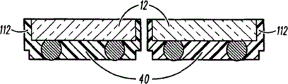
In following step 26, as shown in Figure 8, the support 84 of coupling is put on the active surface of wafer downwards, the correct grinding back side 80 (opposing face of just active surface or band bump surface).Correct grinding is a kind of method of known removal part semiconductor wafer material, and the flat board 82 of mobile exactly wafer by being cast with liquid abrasive is with the quantity thinned wafer of accurate control.Back side correct grinding (back lapping) is widely known by the people in semi-conductor industry.The method of other removal material is suitable for as grinding or polishing too.Process of lapping carries out removing from chip back surface until enough materials always, and so initial cutting only partly enters the groove 38 of wafer, penetrates wafer now fully from the front to the back side, as shown in Figure 9.If by embodiment shown in Figure 5, end filler is not deposited in the groove 38, like this behind the abundant attenuate of thickness quilt of wafer, groove fully from the front to back side through-wafer, the single integrated circuit chip is cut by the correct grinding operation, as shown in figure 10, no longer needs further processing.Yet,, cut step 28 and undertaken by the end filler 92 that cuts off in the groove if end filler is deposited in the groove.This process can be operated from the active surface or the back side of integrated circuit (IC) chip, generally uses laser (excimer, UV, CO
2Or other kind) or the mode of machine cuts or sawing finish.Referring now to Figure 11, after the material 92 in the groove was cut off, single integrated circuit chip 12 broke away from wafers, because the more initial scribing otch of otch is narrow for the second time, end filler 112 still is present on the edge of each chip that the scribing stage 22 forms.In two embodiment, after integrated circuit (IC) chip is cut from wafer, be deposited on filler of the active lip-deep end 40 in step 24 and be retained on the active surface of flip-chip 112.
In a word, as described in the embodiment here, the present invention can implement like this: at the active surperficial cutting-up wafer of wafer, form the groove that finally defines the single integrated circuit chip edge, the degree of depth of cutting-up only reaches the segment thickness of wafer.Use the front of end filler coated wafer then.Generally, the part of each pedestal is not coated, but salient point may be covered fully in some cases.The back side of wafer is finish grinded then, grinds, and polishing or other processing remove material and reach concordant with the groove of initial cutting-up.The groove that the attenuate of wafer thickness forms initial cutting-up (scribing) penetrates the front-back of wafer fully.Wafer is finished and is cut by being breaking at the coating filler of any end of phase deposition in groove subsequently, integrated circuit (IC) chip disengaging wafer like this, and be coated in the active surface that filler of the active lip-deep end is fixed in each single integrated circuit chip.Yet, skilled person in the art will appreciate that said process can be subjected to any change and not break away from the present invention.
A plurality of embodiment have been set forth above.For a person skilled in the art, may make other combination and the change of these embodiment according to instruction of the present invention.Those skilled in the art also can understand, other coating, and scribing, cutting is fluxed, and correct grinding and separating and cutting process can be selected and do not break away from protection scope of the present invention.Alternative method should be used as equivalent and take in.Although the present invention combines specific embodiment and is described, obviously according to previous description, many changes or change apparent to those skilled in the art.Therefore, this just means that the present invention comprises all these replacements or change, and they all drop in protection scope of the present invention.
Claims (27)
1. one kind provides end filler and cuts the method for chip from wafer on integrated circuit (IC) chip, may further comprise the steps successively:
A., one wafer with front and back is provided, and this wafer comprises at least one integrated circuit (IC) chip, and this integrated circuit (IC) chip comprises a plurality of pedestals that are positioned at described front wafer surface;
B. cut the front of described wafer, form groove, this groove defines the edge of described at least one integrated circuit (IC) chip, and cutting reaches the degree of depth of not cutting wafer fully;
C. apply the front of described wafer with end filler;
D. finish grind the back side of wafer, fully the thickness of thinned wafer makes groove extend to described back from described front; And
E. the end filler that wherein is coated on front wafer surface is fixed on the integrated circuit (IC) chip.
2. the method for claim 1 further comprises, after step (c), applies the step of one deck flux on described a plurality of pedestals.
3. method as claimed in claim 2, the step that wherein applies the flux layer are being close to step (c) afterwards and in step (d) before.
4. the method for claim 1, wherein in the coating stage, end filler deposits in the groove and the edge of described integrated circuit (IC) chip.
5. the method for claim 1 is wherein finish grinded step and is comprised grinding, polishing or correct grinding chip back surface.
6. the method for claim 1, wherein said applying step comprise dip-coating, spraying or printing liquid material coating, or lamination forms rete.
7. the method for claim 1, wherein integrated circuit is a flip-chip integrated circuit.
8. the method for claim 1, filler of the wherein said end is selected from the group that comprises epoxy resin, polyimide and silicon-polyimide copolymer.
9. the method for claim 1, wherein said applying step (c) further comprise each described pedestal of coating.
10. the method for claim 1, wherein applying step (c) comprises that a part that keeps each described pedestal is not coated.
11. one kind provides the method for end filler to integrated circuit (IC) chip, comprises the following steps: successively
A., wafer with front and back is provided, and this wafer comprises at least one integrated circuit (IC) chip, and this integrated circuit (IC) chip comprises a plurality of pedestals that are positioned at described front wafer surface;
B. cut the front of described wafer, form groove, this groove defines the edge of described at least one integrated circuit (IC) chip, and cutting reaches not the degree of depth of through-wafer fully;
C. apply the front of described wafer with end filler, a part that keeps each described pedestal is not coated;
D. remove material from the back side of wafer,, make groove extend to described back from described front with the thickness of abundant thinned wafer;
E. divide pellet, promptly by fully cutting off the end filler in the groove, so that integrated circuit (IC) chip is separated from wafer;
F. the end filler that wherein is coated on front wafer surface remains fixed on the integrated circuit (IC) chip after cutting.
12. method as claimed in claim 11 further comprises, after step (c), applies the step of one deck flux on the part of described pedestal uncoated.
13. method as claimed in claim 12, the step that wherein applies the flux layer further is included in and applies one deck flux on the end filler.
14. method as claimed in claim 12, the step that wherein applies the flux layer is being close to after the step c and before steps d.
15. method as claimed in claim 11, wherein in the coating stage, end filler deposit in the groove and the edge of described integrated circuit (IC) chip on.
16. method as claimed in claim 15, wherein cut step after, end filler keeps and to spread on the edge of described integrated circuit (IC) chip.
17. method as claimed in claim 11 is wherein cut step and is comprised with filler at the bottom of the laser cutting, or section or filler of the described end of sawing.
18. method as claimed in claim 11, wherein the step from chip back surface removal material comprises grinding, polishing or correct grinding chip back surface.
19. method as claimed in claim 11, wherein said applying step comprise dip-coating, spraying or printing coating liquid material, or lamination forms rete.
20. method as claimed in claim 11, wherein said integrated circuit is a flip-chip integrated circuit.
21. method as claimed in claim 11, filler of the wherein said end is selected from the group that comprises epoxy resin, polyimide and silicon-polyimide copolymer.
22. method as claimed in claim 11, wherein said cutting step comprises sawing.
23. the wafer scale preparation method that end filler adhesive layer is provided on integrated circuit, this integrated circuit has an active surface, wherein comprises the soldered ball that is positioned on the conductive welding disk, comprising:
The silicon wafer that comprises one or more integrated circuits is provided;
The active surface of cutting-up silicon wafer is to form groove, and this groove defines the edge of described integrated circuit (IC) chip, and cutting reaches not the degree of depth of through-wafer fully;
Filler binding agent at the bottom of formation one deck on the active surface of integrated circuit and in the groove, wherein certain part at least of most of soldered ball is not coated;
Make filler binding agent of the described end partly solidified;
Remove enough silicon materials from the back side of wafer, make groove connect wafer fully; And
Cut off the end filler binding agent that is comprised in the groove, to cut at least one integrated circuit (IC) chip, the active surface and the edge of this chip have end filler.
24. method as claimed in claim 23 further comprises, applies one deck flux on the part of described pedestal uncoated.
25. method as claimed in claim 23, the step that wherein applies the flux layer further is included in and applies one deck flux on the end filler.
26. method as claimed in claim 23, wherein the step from chip back surface removal silicon materials comprises grinding, polishing or correct grinding chip back surface.
27. the method that end filler adhesive layer is provided on the wafer with band salient point integrated circuit (IC) array, each circuit comprises active surface, comprises soldered ball on its conductive welding disk, comprising:
To form groove, the predetermined depth of this groove is less than the degree of depth of wafer at the described wafer of salient point side cutting-up;
With end filler coated wafer, cover described active surface and the described groove of filling with this end filler;
Polish the opposition side on active surface on the described wafer, the groove that forms until scribing connects wafer;
Cut off the end filler in the described groove, to cut the integrated circuit (IC) array of band salient point.
Applications Claiming Priority (2)
| Application Number | Priority Date | Filing Date | Title |
|---|---|---|---|
| US10/241,265 | 2002-09-11 | ||
| US10/241,265 US6649445B1 (en) | 2002-09-11 | 2002-09-11 | Wafer coating and singulation method |
Publications (2)
| Publication Number | Publication Date |
|---|---|
| CN1682363A CN1682363A (en) | 2005-10-12 |
| CN100416768C true CN100416768C (en) | 2008-09-03 |
Family
ID=29420109
Family Applications (1)
| Application Number | Title | Priority Date | Filing Date |
|---|---|---|---|
| CNB038214520A Expired - Fee Related CN100416768C (en) | 2002-09-11 | 2003-09-05 | Wafer coating and singulation method |
Country Status (6)
| Country | Link |
|---|---|
| US (1) | US6649445B1 (en) |
| JP (1) | JP2005538572A (en) |
| KR (1) | KR101054238B1 (en) |
| CN (1) | CN100416768C (en) |
| AU (1) | AU2003296904A1 (en) |
| WO (1) | WO2004034422A2 (en) |
Families Citing this family (74)
| Publication number | Priority date | Publication date | Assignee | Title |
|---|---|---|---|---|
| US6352881B1 (en) | 1999-07-22 | 2002-03-05 | National Semiconductor Corporation | Method and apparatus for forming an underfill adhesive layer |
| US6794751B2 (en) * | 2001-06-29 | 2004-09-21 | Intel Corporation | Multi-purpose planarizing/back-grind/pre-underfill arrangements for bumped wafers and dies |
| DE10202881B4 (en) * | 2002-01-25 | 2007-09-20 | Infineon Technologies Ag | Method for producing semiconductor chips with a chip edge protection layer, in particular for wafer level packaging chips |
| US6908784B1 (en) * | 2002-03-06 | 2005-06-21 | Micron Technology, Inc. | Method for fabricating encapsulated semiconductor components |
| US7423337B1 (en) | 2002-08-19 | 2008-09-09 | National Semiconductor Corporation | Integrated circuit device package having a support coating for improved reliability during temperature cycling |
| US6903442B2 (en) | 2002-08-29 | 2005-06-07 | Micron Technology, Inc. | Semiconductor component having backside pin contacts |
| JP2004221125A (en) * | 2003-01-09 | 2004-08-05 | Sharp Corp | Semiconductor device and its manufacturing method |
| US7301222B1 (en) | 2003-02-12 | 2007-11-27 | National Semiconductor Corporation | Apparatus for forming a pre-applied underfill adhesive layer for semiconductor wafer level chip-scale packages |
| JP2004288816A (en) * | 2003-03-20 | 2004-10-14 | Seiko Epson Corp | Semiconductor wafer, semiconductor device and its manufacturing process, circuit board and electronic apparatus |
| US20040235272A1 (en) * | 2003-05-23 | 2004-11-25 | Howard Gregory E. | Scribe street width reduction by deep trench and shallow saw cut |
| US6890836B2 (en) * | 2003-05-23 | 2005-05-10 | Texas Instruments Incorporated | Scribe street width reduction by deep trench and shallow saw cut |
| DE10333841B4 (en) * | 2003-07-24 | 2007-05-10 | Infineon Technologies Ag | A method of producing a benefit having semiconductor device locations arranged in rows and columns and methods of making a semiconductor device |
| TWI231534B (en) * | 2003-12-11 | 2005-04-21 | Advanced Semiconductor Eng | Method for dicing a wafer |
| US7282375B1 (en) | 2004-04-14 | 2007-10-16 | National Semiconductor Corporation | Wafer level package design that facilitates trimming and testing |
| US7364945B2 (en) | 2005-03-31 | 2008-04-29 | Stats Chippac Ltd. | Method of mounting an integrated circuit package in an encapsulant cavity |
| US7354800B2 (en) | 2005-04-29 | 2008-04-08 | Stats Chippac Ltd. | Method of fabricating a stacked integrated circuit package system |
| KR100660868B1 (en) * | 2005-07-06 | 2006-12-26 | 삼성전자주식회사 | Semiconductor package with molded back side and method for fabricating the same |
| US7273768B2 (en) * | 2005-08-30 | 2007-09-25 | Mutual-Pak Technology Co. Ltd. | Wafer-level package and IC module assembly method for the wafer-level package |
| US7768125B2 (en) * | 2006-01-04 | 2010-08-03 | Stats Chippac Ltd. | Multi-chip package system |
| US7456088B2 (en) | 2006-01-04 | 2008-11-25 | Stats Chippac Ltd. | Integrated circuit package system including stacked die |
| JP2007214268A (en) * | 2006-02-08 | 2007-08-23 | Seiko Instruments Inc | Process for fabrication of semiconductor device |
| US7750482B2 (en) | 2006-02-09 | 2010-07-06 | Stats Chippac Ltd. | Integrated circuit package system including zero fillet resin |
| US8704349B2 (en) | 2006-02-14 | 2014-04-22 | Stats Chippac Ltd. | Integrated circuit package system with exposed interconnects |
| JP4791843B2 (en) * | 2006-02-14 | 2011-10-12 | 株式会社ディスコ | Method for manufacturing device with adhesive film |
| US7385299B2 (en) * | 2006-02-25 | 2008-06-10 | Stats Chippac Ltd. | Stackable integrated circuit package system with multiple interconnect interface |
| JP5275553B2 (en) * | 2006-06-27 | 2013-08-28 | スリーエム イノベイティブ プロパティズ カンパニー | Method for manufacturing divided chips |
| US7482251B1 (en) * | 2006-08-10 | 2009-01-27 | Impinj, Inc. | Etch before grind for semiconductor die singulation |
| US9111950B2 (en) * | 2006-09-28 | 2015-08-18 | Philips Lumileds Lighting Company, Llc | Process for preparing a semiconductor structure for mounting |
| JP5091600B2 (en) | 2006-09-29 | 2012-12-05 | 三洋電機株式会社 | Semiconductor module, semiconductor module manufacturing method, and portable device |
| JP4933233B2 (en) | 2006-11-30 | 2012-05-16 | 株式会社ディスコ | Wafer processing method |
| JP4345808B2 (en) * | 2006-12-15 | 2009-10-14 | エルピーダメモリ株式会社 | Manufacturing method of semiconductor device |
| KR100842505B1 (en) * | 2006-12-19 | 2008-07-01 | 동부일렉트로닉스 주식회사 | Metal deposition process of a backside of a semiconductor wafer |
| TWI364793B (en) * | 2007-05-08 | 2012-05-21 | Mutual Pak Technology Co Ltd | Package structure for integrated circuit device and method of the same |
| US7727875B2 (en) * | 2007-06-21 | 2010-06-01 | Stats Chippac, Ltd. | Grooving bumped wafer pre-underfill system |
| US7838424B2 (en) * | 2007-07-03 | 2010-11-23 | Taiwan Semiconductor Manufacturing Company, Ltd. | Enhanced reliability of wafer-level chip-scale packaging (WLCSP) die separation using dry etching |
| US20090155981A1 (en) * | 2007-12-13 | 2009-06-18 | Ayotte Stephen P | Method and apparatus for singulating integrated circuit chips |
| US7824962B2 (en) * | 2008-01-29 | 2010-11-02 | Infineon Technologies Ag | Method of integrated circuit fabrication |
| CN101521164B (en) * | 2008-02-26 | 2011-01-05 | 上海凯虹科技电子有限公司 | Lead-bonding chip-scale packaging method |
| JP5436827B2 (en) * | 2008-03-21 | 2014-03-05 | 日立化成株式会社 | Manufacturing method of semiconductor device |
| US8058150B2 (en) * | 2008-07-10 | 2011-11-15 | Taiwan Semiconductor Manufacturing Company, Ltd. | Particle free wafer separation |
| US7989950B2 (en) | 2008-08-14 | 2011-08-02 | Stats Chippac Ltd. | Integrated circuit packaging system having a cavity |
| JP2010192867A (en) * | 2009-01-20 | 2010-09-02 | Renesas Electronics Corp | Semiconductor integrated circuit device and semiconductor integrated circuit device manufacturing method |
| US7776649B1 (en) * | 2009-05-01 | 2010-08-17 | Powertech Technology Inc. | Method for fabricating wafer level chip scale packages |
| CN101941181B (en) * | 2009-07-03 | 2012-10-17 | 日月光半导体制造股份有限公司 | Method for grinding wafer |
| CN102237307A (en) * | 2010-04-27 | 2011-11-09 | 瑞鼎科技股份有限公司 | Integrated circuit wafer cutting method |
| US9224647B2 (en) | 2010-09-24 | 2015-12-29 | Stats Chippac, Ltd. | Semiconductor device and method of forming TSV interposer with semiconductor die and build-up interconnect structure on opposing surfaces of the interposer |
| US8993377B2 (en) | 2010-09-29 | 2015-03-31 | Stats Chippac, Ltd. | Semiconductor device and method of bonding different size semiconductor die at the wafer level |
| US8652935B2 (en) | 2010-12-16 | 2014-02-18 | Tessera, Inc. | Void-free wafer bonding using channels |
| US20120273935A1 (en) * | 2011-04-29 | 2012-11-01 | Stefan Martens | Semiconductor Device and Method of Making a Semiconductor Device |
| JP5888995B2 (en) | 2012-01-16 | 2016-03-22 | 三菱電機株式会社 | Semiconductor device and manufacturing method thereof |
| US8940618B2 (en) * | 2012-03-13 | 2015-01-27 | Taiwan Semiconductor Manufacturing Company, Ltd. | Method and device for cutting semiconductor wafers |
| CN102825541B (en) * | 2012-09-10 | 2014-12-10 | 豪威科技(上海)有限公司 | Wafer thinning method |
| US9631065B2 (en) * | 2013-03-12 | 2017-04-25 | Intel Corporation | Methods of forming wafer level underfill materials and structures formed thereby |
| US9508623B2 (en) | 2014-06-08 | 2016-11-29 | UTAC Headquarters Pte. Ltd. | Semiconductor packages and methods of packaging semiconductor devices |
| JP5967629B2 (en) | 2014-11-17 | 2016-08-10 | インターナショナル・ビジネス・マシーンズ・コーポレーションInternational Business Machines Corporation | Circuit module and manufacturing method thereof |
| US9466585B1 (en) * | 2015-03-21 | 2016-10-11 | Nxp B.V. | Reducing defects in wafer level chip scale package (WLCSP) devices |
| JP2017054888A (en) * | 2015-09-08 | 2017-03-16 | 株式会社ディスコ | Processing method for wafer |
| US11037904B2 (en) | 2015-11-24 | 2021-06-15 | Taiwan Semiconductor Manufacturing Company, Ltd. | Singulation and bonding methods and structures formed thereby |
| JP6608694B2 (en) * | 2015-12-25 | 2019-11-20 | 株式会社ディスコ | Wafer processing method |
| JP6523999B2 (en) * | 2016-03-14 | 2019-06-05 | 東芝メモリ株式会社 | Semiconductor device and method of manufacturing the same |
| JP6767814B2 (en) * | 2016-09-05 | 2020-10-14 | 株式会社ディスコ | Manufacturing method of packaged device chip |
| JP6746224B2 (en) * | 2016-11-18 | 2020-08-26 | 株式会社ディスコ | Device chip package manufacturing method |
| US10529671B2 (en) | 2016-12-13 | 2020-01-07 | Taiwan Semiconductor Manufacturing Co., Ltd. | Package structure and method for forming the same |
| US10510709B2 (en) * | 2017-04-20 | 2019-12-17 | Taiwan Semiconductor Manufacturing Co., Ltd. | Semicondcutor package and manufacturing method thereof |
| CN109102772B (en) * | 2017-06-20 | 2023-11-21 | 昆山国显光电有限公司 | Driving circuit board and display device |
| JP7013085B2 (en) * | 2017-09-08 | 2022-01-31 | 株式会社ディスコ | Wafer processing method |
| JP6976650B2 (en) * | 2017-09-08 | 2021-12-08 | 株式会社ディスコ | Wafer processing method |
| JP7058904B2 (en) * | 2017-09-08 | 2022-04-25 | 株式会社ディスコ | Wafer processing method |
| JP7013084B2 (en) * | 2017-09-08 | 2022-01-31 | 株式会社ディスコ | Wafer processing method |
| JP6918418B2 (en) * | 2017-09-08 | 2021-08-11 | 株式会社ディスコ | Wafer processing method |
| JP7118522B2 (en) * | 2017-09-19 | 2022-08-16 | 株式会社ディスコ | Wafer processing method |
| JP7118521B2 (en) * | 2017-09-19 | 2022-08-16 | 株式会社ディスコ | Wafer processing method |
| KR102506698B1 (en) * | 2018-02-19 | 2023-03-07 | 에스케이하이닉스 주식회사 | Method of fabricating semiconductor package including reinforcement top die |
| US11908831B2 (en) | 2020-10-21 | 2024-02-20 | Stmicroelectronics Pte Ltd | Method for manufacturing a wafer level chip scale package (WLCSP) |
Citations (3)
| Publication number | Priority date | Publication date | Assignee | Title |
|---|---|---|---|---|
| US6107164A (en) * | 1998-08-18 | 2000-08-22 | Oki Electric Industry Co., Ltd. | Using grooves as alignment marks when dicing an encapsulated semiconductor wafer |
| US6184109B1 (en) * | 1997-07-23 | 2001-02-06 | Kabushiki Kaisha Toshiba | Method of dividing a wafer and method of manufacturing a semiconductor device |
| CN1337065A (en) * | 1999-11-11 | 2002-02-20 | 卡西欧计算机株式会社 | Semiconductor device and method of mfg. the same |
Family Cites Families (21)
| Publication number | Priority date | Publication date | Assignee | Title |
|---|---|---|---|---|
| US5128746A (en) | 1990-09-27 | 1992-07-07 | Motorola, Inc. | Adhesive and encapsulant material with fluxing properties |
| JP3376203B2 (en) | 1996-02-28 | 2003-02-10 | 株式会社東芝 | Semiconductor device, method of manufacturing the same, mounting structure using the semiconductor device, and method of manufacturing the same |
| JP3137322B2 (en) * | 1996-07-12 | 2001-02-19 | 富士通株式会社 | Semiconductor device manufacturing method, semiconductor device manufacturing mold, and semiconductor device |
| AU8502798A (en) | 1997-07-21 | 1999-02-10 | Aguila Technologies, Inc. | Semiconductor flip-chip package and method for the fabrication thereof |
| JPH11111646A (en) * | 1997-10-02 | 1999-04-23 | Fujitsu Ltd | Manufacture of semiconductor device and semiconductor device |
| US6265776B1 (en) * | 1998-04-27 | 2001-07-24 | Fry's Metals, Inc. | Flip chip with integrated flux and underfill |
| US6323062B1 (en) | 1998-04-27 | 2001-11-27 | Alpha Metals, Inc. | Wafer coating method for flip chips |
| US6168972B1 (en) | 1998-12-22 | 2001-01-02 | Fujitsu Limited | Flip chip pre-assembly underfill process |
| JP3330890B2 (en) * | 1999-01-12 | 2002-09-30 | 沖電気工業株式会社 | Resin-sealed semiconductor device and method of manufacturing the same |
| US6194788B1 (en) | 1999-03-10 | 2001-02-27 | Alpha Metals, Inc. | Flip chip with integrated flux and underfill |
| JP3423245B2 (en) * | 1999-04-09 | 2003-07-07 | 沖電気工業株式会社 | Semiconductor device and mounting method thereof |
| US6352881B1 (en) * | 1999-07-22 | 2002-03-05 | National Semiconductor Corporation | Method and apparatus for forming an underfill adhesive layer |
| JP2001127206A (en) * | 1999-08-13 | 2001-05-11 | Citizen Watch Co Ltd | Manufacturing method of chip-scale package and manufacturing method of ic chip |
| US6524890B2 (en) * | 1999-11-17 | 2003-02-25 | Denso Corporation | Method for manufacturing semiconductor device having element isolation structure |
| JP2001176899A (en) * | 1999-12-21 | 2001-06-29 | Sanyo Electric Co Ltd | Manufacturing method for semiconductor device |
| JP4438973B2 (en) | 2000-05-23 | 2010-03-24 | アムコア テクノロジー,インコーポレイテッド | Sheet-shaped resin composition and method for manufacturing semiconductor device using the same |
| US6528393B2 (en) * | 2000-06-13 | 2003-03-04 | Advanced Semiconductor Engineering, Inc. | Method of making a semiconductor package by dicing a wafer from the backside surface thereof |
| JP2002016022A (en) * | 2000-06-29 | 2002-01-18 | Toshiba Corp | Method of manufacturing semiconductor device |
| JP2002100709A (en) * | 2000-09-21 | 2002-04-05 | Hitachi Ltd | Semiconductor device and manufacturing method thereof |
| US6506681B2 (en) | 2000-12-06 | 2003-01-14 | Micron Technology, Inc. | Thin flip—chip method |
| JP4330821B2 (en) * | 2001-07-04 | 2009-09-16 | 株式会社東芝 | Manufacturing method of semiconductor device |
-
2002
- 2002-09-11 US US10/241,265 patent/US6649445B1/en not_active Expired - Lifetime
-
2003
- 2003-09-05 JP JP2004543275A patent/JP2005538572A/en active Pending
- 2003-09-05 WO PCT/US2003/027964 patent/WO2004034422A2/en active Application Filing
- 2003-09-05 KR KR1020057004220A patent/KR101054238B1/en not_active IP Right Cessation
- 2003-09-05 CN CNB038214520A patent/CN100416768C/en not_active Expired - Fee Related
- 2003-09-05 AU AU2003296904A patent/AU2003296904A1/en not_active Abandoned
Patent Citations (3)
| Publication number | Priority date | Publication date | Assignee | Title |
|---|---|---|---|---|
| US6184109B1 (en) * | 1997-07-23 | 2001-02-06 | Kabushiki Kaisha Toshiba | Method of dividing a wafer and method of manufacturing a semiconductor device |
| US6107164A (en) * | 1998-08-18 | 2000-08-22 | Oki Electric Industry Co., Ltd. | Using grooves as alignment marks when dicing an encapsulated semiconductor wafer |
| CN1337065A (en) * | 1999-11-11 | 2002-02-20 | 卡西欧计算机株式会社 | Semiconductor device and method of mfg. the same |
Also Published As
| Publication number | Publication date |
|---|---|
| WO2004034422A3 (en) | 2004-08-26 |
| JP2005538572A (en) | 2005-12-15 |
| WO2004034422A2 (en) | 2004-04-22 |
| KR101054238B1 (en) | 2011-08-08 |
| AU2003296904A8 (en) | 2004-05-04 |
| KR20050054933A (en) | 2005-06-10 |
| US6649445B1 (en) | 2003-11-18 |
| AU2003296904A1 (en) | 2004-05-04 |
| CN1682363A (en) | 2005-10-12 |
Similar Documents
| Publication | Publication Date | Title |
|---|---|---|
| CN100416768C (en) | Wafer coating and singulation method | |
| US8030769B2 (en) | Grooving bumped wafer pre-underfill system | |
| US7064010B2 (en) | Methods of coating and singulating wafers | |
| US7501300B2 (en) | Manufacturing method of semiconductor integrated circuit device | |
| US5863813A (en) | Method of processing semiconductive material wafers and method of forming flip chips and semiconductor chips | |
| US6534341B2 (en) | Methods of wafer level fabrication and assembly of chip scale packages | |
| US7838391B2 (en) | Ultra thin bumped wafer with under-film | |
| US6251705B1 (en) | Low profile integrated circuit packages | |
| US20110062592A1 (en) | Delamination Resistance of Stacked Dies in Die Saw | |
| CN102468248B (en) | Protecting flip-chip package using pre-applied fillet | |
| JP2008235401A (en) | Semiconductor device and manufacturing method therefor | |
| US20140117568A1 (en) | Structure of wafer level chip molded package | |
| US9153566B1 (en) | Semiconductor device manufacturing method and semiconductor device | |
| JP2005064499A (en) | Method of manufacturing semiconductor device | |
| CN101752274A (en) | Method of manufacturing semiconductor device | |
| JP2001053033A (en) | Dicing method of semiconductor device | |
| JP2007123719A (en) | Semiconductor chip and its manufacturing method as well as semiconductor device | |
| JP2002016022A (en) | Method of manufacturing semiconductor device | |
| US7086394B2 (en) | Grindable self-cleaning singulation saw blade and method | |
| JP2000340530A (en) | Semiconductor device and manufacture thereof | |
| JP4778667B2 (en) | Sheet material for underfill, semiconductor chip underfill method, and semiconductor chip mounting method | |
| CN101086952A (en) | Wafer package body and crystal circle processing method for making wafer with rubber layer | |
| KR100994477B1 (en) | Back grinding and sawing method for wafer | |
| JP5087995B2 (en) | Semiconductor device and manufacturing method thereof | |
| JP2001007052A (en) | Division of substrate |
Legal Events
| Date | Code | Title | Description |
|---|---|---|---|
| C06 | Publication | ||
| PB01 | Publication | ||
| C10 | Entry into substantive examination | ||
| SE01 | Entry into force of request for substantive examination | ||
| C14 | Grant of patent or utility model | ||
| GR01 | Patent grant | ||
| CF01 | Termination of patent right due to non-payment of annual fee |
Granted publication date: 20080903 Termination date: 20180905 |
|
| CF01 | Termination of patent right due to non-payment of annual fee |