The explanation of most preferred embodiment
Below, specific embodiments of the invention are described with reference to the accompanying drawings.
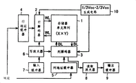
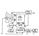
The one-piece construction of strong dielectric memory of the simple matrix mode of embodiment 1 at first, is described with reference to Fig. 1.Read-out amplifier 8, output buffer 9 and 1/3Vcc2/3Vcc generative circuit 10 that the strong dielectric memory of embodiment 1 has memory cell array 1, row decoder 2, column decoder 3, row address buffer 4, column address buffer 5, write amplifier 6, input buffer 7, is made of the voltage sensor amplifier.
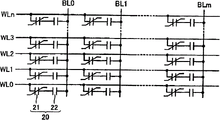
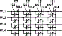
Memory cell array 1 comprises the memory cell of a plurality of simple matrix modes that only are made of strong dielectric electric capacity (not shown).Promptly, the memory cell of the simple matrix mode of embodiment 1 is the same with the memory cell of existing simple matrix mode shown in Figure 61, by word line WL that extends to form along direction intersected with each other and bit line BL, be configured in the strong dielectric electric capacity (not shown) that the strong dielectric film (not shown) between word line WL and the bit line BL constitutes and constitute.This strong dielectric electric capacity is an example of the 1st memory unit of the present invention.On the word line WL of memory cell array 1, connect row decoder 2, on bit line BL, connect column decoder 3.On row decoder 2 and column decoder 3, be connected 1/3Vcc2/3Vcc generative circuit 10.Thereby, can apply 1/3Vcc and 2/3Vcc to non-selection word line WL (non-selection WL) and non-selection bit line BL (non-selection BL).In addition, row decoder 2 and column decoder 5 can constitute to selecting word line WL (selecting WL) and selecting bit line BL (selecting BL) to apply Vcc (supply voltage or the voltage that generates according to supply voltage) and 0V.
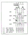
As shown in Figure 2, constitute the 1/3Vcc2/3Vcc generative circuit by making up two 1/2Vcc generative circuit 40a and 40b.1/2Vcc generative circuit 40a and 40b have two sub-50a of voltage input end (50b) and a 51a (51b) and a sub-52a of voltage output end (52b).In addition, apply Vcc to the sub-50a of voltage input end of the 1/2Vcc of side generative circuit 40a, the sub-51a of voltage input end is connected with the sub-52b of voltage output end of the 1/2Vcc generative circuit 40b of opposite side.In addition, the sub-52a of voltage output end of the 1/2Vcc generative circuit 40a of a side is connected with the sub-50b of voltage input end of the 1/2Vcc generative circuit 40b of opposite side.The sub-51b of voltage input end to the 1/2Vcc of opposite side generative circuit 40b applies 0V.
By formation like this, obtain 2/3Vcc as the medium voltage of Vcc and 1/3Vcc from the sub-62a of voltage output end (the sub-52a of voltage output end of the 1/2Vcc generative circuit 40a of a side) of 1/3Vcc2/3Vcc generative circuit one side.In addition, the sub-62b of the voltage output end of opposite side (the sub-52b of voltage output end of the 1/2Vcc generative circuit 40b of opposite side) obtains the 1/3Vcc as the medium voltage of 2/3Vcc and 0V.
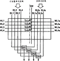
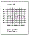
Below, illustrate with reference to Fig. 3-Fig. 6 embodiment 1 the simple matrix mode the strong dielectric memory unit read action and write activity again.In this action specification, be selected cell with the 4th cell descriptions that is positioned on word line WL2 and the bit line BL2 intersection point shown in Figure 3.
The voltage waveform that applies to word line WL and bit line BL shown in Fig. 4.Be made as respectively the identical time (T second) each actuation time of (1) shown in Fig. 4, (2), (3) and (4).In addition, each action of (1)-(4) both can from (1) to (4) be carried out continuously, also can independently carry out respectively.Below, illustrate (1)-each action in (4).Under waiting status, establishing word line WL and bit line BL is 0V.
(1) reads action
Read action in during (1) shown in Figure 4.At first, select BL to become quick condition from waiting status.Under identical timing, select WL to become Vcc, non-selection WL becomes 1/3Vcc, and non-selection BL becomes 2/3Vcc.Under this state,, carry out the judgement of data [0] or data [1] by detecting the voltage of selecting BL.By by as the read-out amplifier 8 (with reference to Fig. 1) of voltage sensor amplifier relatively and amplify the current potential of selecting BL and generate in addition with reference to current potential, carry out the judgement of data [0] or [1].Reading in the action of this (1), apply following potential difference (PD) T second to unit, the 1st unit-the 4th (with reference to Fig. 3).
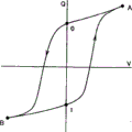
That is, reading in the action of (1), to selecting Unit the 1st of the non-selected cell on WL and the non-selection BL intersection point to apply T 1/3Vcc second potential difference (PD) as shown in Figure 3 being positioned at.In addition, be positioned at non-selection wire WL and select Unit the 2nd of the non-selected cell on the BL intersection point to apply T 1/3Vcc-second selection BL current potential (floating potential) to conduct.Apply T second-1/3Vcc potential difference (PD) to Unit the 3rd that conduct is positioned at the non-selected cell on non-selection WL and the non-selection BL intersection point.Be positioned at Unit the 4th of selecting WL and selecting the selected cell on the BL intersection point to conduct and apply the potential difference (PD) that T Vcc-second selects BL current potential (floating potential).At this moment, in non-selected cell (unit, the 1st unit-the 3rd), keep producing the deterioration and the improvement of polarized state under next data conditions.Here, the deterioration of so-called polarized state is meant and has reduced charge stored amount in the strong dielectric electric capacity that the improvement of so-called polarized state is meant has increased the quantity of electric charge that reduces.
In Unit the 1st, keep under the situation of data [1], produce the deterioration of polarized state, under the situation that keeps data [0], produce the improvement of polarized state as non-selected cell.In Unit the 2nd, keep under the situation of data [1], produce the deterioration of polarized state, under the situation that keeps data [0], produce the improvement of polarized state as non-selected cell.In Unit the 3rd, keep under the situation of data [1], produce the improvement of polarized state, under the situation that keeps data [0], produce the deterioration of polarized state as non-selected cell.In Unit the 4th, keep under the situation of data [1], produce the deterioration of polarized state, under the situation that keeps data [0], write data [0] once more as selected cell.
(2) [1] write activity again
Above-mentioned (1) read action after, temporarily return waiting status.Afterwards, select WL to become 0V, non-selection WL becomes 2/3Vcc, selects BL to become Vcc, and non-selection BL becomes 1/3Vcc.At this moment, in second, applying following potential difference (PD) as the T during the action of (2) to unit, the 1st unit-the 4th.That is, to Unit the 1st, Unit the 2nd and Unit the 3rd as non-selected cell apply respectively T second-1/3Vcc ,-1/3Vcc and 1/3Vcc.Thereby, in Unit the 1st, keep under the situation of data [1] as non-selected cell, produce the improvement of polarized state, under the situation that keeps data [0], produce the deterioration of polarized state.In Unit the 2nd, keep under the situation of data [1], produce the improvement of polarized state, under the situation that keeps data [0], produce the deterioration of polarized state as non-selected cell.In Unit the 3rd, keep under the situation of data [1], produce the deterioration of polarized state, under the situation that keeps data [0], produce the improvement of polarized state as non-selected cell.
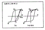
In addition, in Unit the 4th, because apply the potential difference (PD) of T second-Vcc, so under the situation that reads reading of data in the action [1] of (1), in the action of (2), finish the write activity again of data [1] as selected cell.Shown in Fig. 5 in Unit the 4th as selected cell, the variation from the action of (1) of the situation that keeps data [1] to the polarized state of the action of (2).Under the situation of selected cell reading of data [1], finish constantly to read and write activity again at this.
(3) [0] writes and uses compensating movement
Again behind the write activity, temporarily return waiting status in [1] of above-mentioned (2).Afterwards, select WL to become 0V, non-selection WL becomes 2/3Vcc, selects BL to become Vcc, and non-selection BL becomes 1/3Vcc.At this moment, apply following potential difference (PD) T second to unit, the 1st unit-the 4th.Particularly, to Unit the 1st, Unit the 2nd and Unit the 3rd as non-selected cell apply respectively T second-1/3Vcc ,-potential difference (PD) of 1/3Vcc and 1/3Vcc.In addition, to the potential difference (PD) that applies T second-Vcc as Unit the 4th of selected cell.By applying potential difference (PD), in Unit the 1st, keep under the situation of data [1] as non-selected cell, produce the improvement of polarized state, under the situation that keeps data [0], produce the deterioration of polarized state.In Unit the 2nd, keep under the situation of data [1], produce the improvement of polarized state, under the situation that keeps data [0], produce the deterioration of polarized state as non-selected cell.In Unit the 3rd, keep under the situation of data [1], produce the deterioration of polarized state, under the situation that keeps data [0], produce the improvement of polarized state as non-selected cell.In addition, in Unit the 4th,, become the state that writes data [1] once more though the data that keep constantly in above-mentioned (2) become [1] as selected cell.
(4) [0] write activity again
After [0] of above-mentioned (3) writes with compensating movement again, temporarily return waiting status.Afterwards, select WL to become Vcc, non-selection WL becomes 1/3Vcc, selects BL to become 0V, and non-selection BL becomes 2/3Vcc.Thus, to Unit the 1st, Unit the 2nd and Unit the 3rd as non-selected cell apply respectively T 1/3Vcc second, 1/3Vcc and-potential difference (PD) of 1/3Vcc.In addition, to the potential difference (PD) that applies T Vcc second as Unit the 4th of selected cell.Thereby, in Unit the 1st, keep under the situation of data [1] as non-selected cell, produce the deterioration of polarized state, under the situation that keeps data [0], produce the improvement of polarized state.In Unit the 2nd, keep under the situation of data [1], produce the deterioration of polarized state, under the situation that keeps data [0], produce the improvement of polarized state as non-selected cell.In Unit the 3rd, keep under the situation of data [1], produce the improvement of polarized state, under the situation that keeps data [0], produce the deterioration of polarized state as non-selected cell.In Unit the 4th, because apply the potential difference (PD) of Vcc, so become the state that writes data [0] again as selected cell.
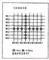
In Unit the 4th, keep the variation of polarized state in the action of above-mentioned (1)-(4) under the situation of [0] shown in Fig. 6 as selected cell.By the action of (4), finish a series of reading and write activity again.The deterioration of polarized state and improvement situation are shown in following table 2 in the action of above-mentioned (1)-(4).
Table 2
*: polarization worsens
Zero: polarization improves
In embodiment 1,, under the situation of reading of data [0], advance to the action of (4) reading and again in the write activity, under the situation of reading of data [1], advancing to the action of (2).Afterwards, move to reading and write activity more next time respectively.In embodiment 1, under these two situations of situation of the situation of reading of data [1] and reading of data [0], the number of times that polarized state worsens equates with the number of times of polarized state improvement.Therefore, even read action and write activity more repeatedly, so the deterioration that also can't accumulate polarized state in non-selected cell is the final data that can not destroy maintenance.
Promptly, in the foregoing description 1, by reading action and write activity again, the direction that the polarized state that causes along the interference of offsetting non-selected cell worsens, Unit the 1st and Unit the 3rd in non-selected cell apply ± 1/3Vcc alternately, simultaneously, the Unit the 2nd in non-selected cell apply alternately 1/3Vcc-select the current potential of bit line and 1/3Vcc ,-1/3Vcc, can effectively suppress the data corruption that polarized state worsens the non-selected cell that causes.
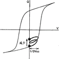
In addition, in the foregoing description 1, set Vcc, make as the 1/3Vcc that is applied to the magnitude of voltage on the non-selected cell to become the reactance voltage of considering less than the hysteresis characteristic that has from the memory cell that constitutes strong dielectric memory (polarization reversal voltage).Thereby, can reduce the deterioration amount that finally occurs in the polarized state in the non-selected cell.This point below the explanation embodiment 2-8 in too.
(embodiment 2)
With reference to Fig. 7, in embodiment 2, the action of (2)-(4) is the same with the foregoing description 1, and only the action of (1) is different with embodiment 1.Below, the action of embodiment 2 is described.In embodiment 2, the same with the foregoing description 1, (1)-(4) are made as respectively the identical time (T second) each actuation time.In addition, each action of (1)-(4) both can from (1) to (4) be carried out continuously, also can independently carry out respectively.Under waiting status, establishing word line WL and bit line BL is 0V.
(1) reads action
The reading in the action of (1) in embodiment 2 selects WL to become Vcc from waiting status, and non-selection WL becomes 1/3Vcc from waiting status, selects BL to become 0V from waiting status, and non-selection BL becomes 2/3Vcc from waiting status.From this state, in embodiment 2,, carry out the judgement of data [0] or data [1] by detecting the electric current that flows through among the selection WL.That is, in the foregoing description 1, carry out the data judgement, but in embodiment 2, come judgment data by detecting the electric current of selecting to flow through among the WL by detecting the voltage of selecting BL.Particularly, by relatively and amplify to select the electric current of WL and generate in addition with reference to electric current, carry out the judgement of data [0] or [1].At this moment, use the read-out amplifier (not shown) that constitutes by the electric current sensor amplifier to replace the read-out amplifier (with reference to Fig. 1) that constitutes by the voltage sensor amplifier among the embodiment 1.Here, flow through the current value transient changing of selecting WL.Therefore, be easy to act as most when flowing through the current value of selecting WL and reaching peak value,, carry out the judgement of data [0] or [1] by comparing and enlarging with reference current value.
Reading in the action of (1), to Unit the 1st, Unit the 2nd and Unit the 3rd as non-selected cell apply respectively T 1/3Vcc second, 1/3Vcc and-potential difference (PD) of 1/3Vcc.In addition, to the potential difference (PD) that applies T Vcc second as Unit the 4th of selected cell.Thereby, in Unit the 1st, keep under the situation of data [1] as non-selected cell, produce the deterioration of polarized state, under the situation that keeps data [0], produce the improvement of polarized state.In Unit the 2nd, keep under the situation of data [1], produce the deterioration of polarized state, under the situation that keeps data [0], produce the improvement of polarized state as non-selected cell.In Unit the 3rd, keep under the situation of data [1], produce the improvement of polarized state, under the situation that keeps data [0], produce the deterioration of polarized state as non-selected cell.In Unit the 4th, keep under the situation of data [1], produce the deterioration of polarized state, under the situation that keeps data [0], write data [0] once more as selected cell.
Reading in the action of embodiment 2 (1), different with the foregoing description 1, because will select the current potential of BL to be fixed on 0V, be positioned at non-selection WL and select the potential difference (PD) of the Unit the 2nd on the BL intersection point to become 1/3Vcc really so be applied to.That is in embodiment 1, be that 1/3Vcc-selects the BL current potential because be positioned at non-selection WL and select the potential difference (PD) of the Unit the 2nd on the BL intersection point,, so by selecting the variation of BL current potential, (or less than 0V) obtains the value of 1/3Vcc near 0V.Therefore, in embodiment 1, in non-selected cell, be arranged in non-selection WL and Unit the 2nd of selecting on the BL intersection point, may not keep the polarized state of data [1] situation to worsen the polarized state improvement action of moving and keeping data [0] situation really.
On the contrary, in embodiment 2, because will select the current potential of BL to be fixed on 0V, so, can keep the polarized state of data [1] situation to worsen action and keep the polarized state of data [0] situation to improve action really as being connected in Unit the 2nd of selecting the non-selected cell on the BL.Thereby, in embodiment 2, even, worsen accumulation because can suppress polarized state really, so it is destroyed finally to be suppressed at the data that keep in Unit the 2nd as being connected in Unit the 2nd of selecting the non-selected cell on the BL.
The action of (2) among the embodiment 2-(4) is the same with the foregoing description 1.
(embodiment 3)
With reference to Fig. 8, in embodiment 3, the action of (2)-(4) is the same with the foregoing description 1, and only the action of (1) is different with embodiment 1.Below, the action of embodiment 3 is described.In embodiment 3, also the same with the foregoing description 1, (1)-(4) are made as respectively the identical time (T second) each actuation time.In addition, each action of (1)-(4) both can from (1) to (4) be carried out continuously, also can independently carry out respectively.Under waiting status, establishing word line WL and bit line BL is 0V.
(1) reads action
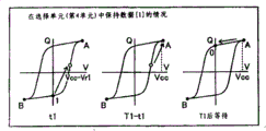
The reading in the action of (1) in embodiment 3 selects BL to become unsteady from waiting status.Under same timing, select WL to become Vcc, non-selection WL becomes 1/3Vcc, and non-selection BL becomes 2/3Vcc.Under this state,, carry out the judgement of data [0] or data [1] by detecting the voltage of selecting BL.By use the read-out amplifier 8 (with reference to Fig. 1) that constitutes by the voltage sensor amplifier relatively and amplify the current potential of selecting BL and generate in addition with reference to current potential, carry out the judgement of data [0] or [1].And, in embodiment 3, after the judgement of data [0] or [1] finishes, select BL to return 0V again.To be made as T second during the action of (1), the time of selecting BL to become quick condition is made as t1 second.
At this moment, apply T 1/3Vcc second potential difference (PD) to Unit the 1st as non-selected cell.In addition, be positioned at non-selection wire WL and select Unit the 2nd of the non-selected cell on the BL intersection point to apply t1 1/3Vcc-second selection BL current potential, simultaneously, apply the potential difference (PD) of T-t1 1/3Vcc second to conduct.In addition, apply T second-1/3Vcc potential difference (PD) to Unit the 3rd that conduct is positioned at the non-selected cell on non-selection WL and the non-selection BL intersection point.On the other hand, after the Unit the 4th as selected cell applies t1 Vcc-second selection BL current potential, apply the potential difference (PD) of T-t1 Vcc second.
Above-mentioned t1 is set to the time t1 of abundant weak point second, with as being arranged in non-selection wire WL and selecting Unit the 2nd of the non-selected cell on the BL intersection point, compare with the amount of polarization variation that the 1/3Vcc that accepts during the T1-t1 causes, the 1/3Vcc-that accepts during t1 selects the electrode quantitative changeization that causes of BL current potential enough little, and, by applying T-t1 1/3Vcc second, the amount of polarization of (1) become with (1) after (2)-(4) in the amount of polarization that takes place change essentially identical amount.Therefore, reading in the action of (1), can following variation polarized state.That is, in Unit the 1st, keep under the situation of data [1], produce the deterioration of polarized state, under the situation that keeps data [0], produce the improvement of polarized state as non-selected cell.In Unit the 2nd, keep under the situation of data [1], produce the deterioration of polarized state, under the situation that keeps data [0], produce the improvement of polarized state as non-selected cell.In Unit the 3rd, keep under the situation of data [1], produce the improvement of polarized state, under the situation that keeps data [0], produce the deterioration of polarized state as non-selected cell.In Unit the 4th, keep under the situation of data [1], produce the deterioration of polarized state, under the situation that keeps data [0], write data [0] once more as selected cell.
The action of (2) among the embodiment 3-(4) is the same with the foregoing description 1.
In embodiment 3, as mentioned above,, after detect selecting the current potential of BL, by being made as 0V, being arranged in non-selection wire WL and selecting Unit the 2nd on the BL intersection point reading in the action of (1), reading with regard to the action of (1) just, generation become 1/3Vcc during.Thereby, in embodiment 3, reading in the action of (1), even, also can keep the polarized state of the situation of data [1] to worsen action and keep the polarized state of the situation of data [0] to improve action really as being connected in Unit the 2nd of selecting the non-selected cell on the BL.
(embodiment 4)
In embodiment 4, carry out the action of reading of (1) in the foregoing description 2 by (1) and (2).Below, the action of (1) and (2) of embodiment 4 is described.In addition, in embodiment 4, the voltage waveform that is applied on word line WL and the bit line BL is the same with embodiment illustrated in fig. 72 voltage oscillogram.In addition, the action of embodiment 4 (3) and (4) is the same with the foregoing description 1.Below, the action of embodiment 4 is described.
(1) select the current value of WL to keep action
In embodiment 4, select WL to become Vcc from waiting status, non-selection WL becomes 1/3Vcc from waiting status, selects BL to become 0V from waiting status, and non-selection BL becomes 2/3Vcc from waiting status.Under this state, in current value holding circuit (not shown), keep the electric current that flows through among the selection WL.Change because flow through the current transient of selecting WL, so the value the when electric current that preferably keeps flowing through reaches peak value.Current value at the selection WL of (1) keeps in the action, respectively to Unit the 1st, Unit the 2nd and Unit the 3rd as non-selected cell apply T 1/3Vcc second, 1/3Vcc and-potential difference (PD) of 1/3Vcc.In addition, to the potential difference (PD) that applies T Vcc second as Unit the 4th of selected cell.
Thereby, keeping under the situation of data [1] as being connected in Unit the 1st of selecting the non-selected cell on the WL, the deterioration that produces polarized state produces the improvement of polarized state under the situation that keeps data [0].Keeping under the situation of data [1] as being connected in Unit the 2nd of selecting the non-selected cell on the BL, produce the deterioration of polarized state, under the situation that keeps data [0], produce the improvement of polarized state.In as the Unit the 3rd that is connected the non-selected cell on non-selection WL and the non-selection BL, keep under the situation of data [1], produce the improvement of polarized state, under the situation that keeps data [0], produce the deterioration of polarized state.In Unit the 4th, write data [0] as selected cell.
(2) select the current value of BL to keep, read, [1] write activity again
Select WL to become 0V from waiting status, non-selection WL becomes 2/3Vcc from waiting status, selects BL to become Vcc from waiting status, and non-selection BL becomes 1/3Vcc from waiting status.Under this state, in current value holding circuit (not shown), keep the electric current that flows through among the selection BL.Change because flow through the current transient of selecting BL, so the value the when electric current that preferably keeps flowing through reaches peak value.The current value of the selection WL that keeps in the current value of the selection BL that keeps in the action by comparison (2) and the action of above-mentioned (1) carries out the judgement of data [0] or [1].At this moment, use the read-out amplifier (not shown) that constitutes by the electric current sensor amplifier to replace the read-out amplifier 8 (with reference to Fig. 1) that constitutes by the voltage sensor amplifier among the embodiment 1.
Here, keep under the situation of data [1] in the Unit the 4th as selected cell, polarized state counter-rotating in the action of (1) and (2) is so in the action of (1) and (2), selecting WL and selecting to flow through same current respectively among the BL.In addition, keep in selected cell under the situation of data [0], only polarized state counter-rotating in the action of (2) is so in the action of (1) and (2), have nothing in common with each other at the current value of selecting WL and select to flow through among the BL.Therefore, in the action of (1), flow through under the current value of the selecting WL situation identical with the current value that in the action of (2), flows through selection BL, be judged as data [1], in the action of (1), flow through under the current value of the selecting WL situation different, be judged as data [0] with the current value that in the action of (2), flows through selection BL.
In the action of (2), to Unit the 1st, Unit the 2nd and Unit the 3rd as non-selected cell apply respectively T second-1/3Vcc ,-potential difference (PD) of 1/3Vcc and 1/3Vcc.In addition, to the potential difference (PD) that applies T second-Vcc as Unit the 4th of selected cell.Thereby, in Unit the 1st, keep under the situation of data [1] as non-selected cell, produce the improvement of polarized state, under the situation that keeps data [0], produce the deterioration of polarized state.In Unit the 2nd, keep under the situation of data [1], produce the improvement of polarized state, under the situation that keeps data [0], produce the deterioration of polarized state as non-selected cell.In Unit the 3rd, keep under the situation of data [1], produce the deterioration of polarized state, under the situation that keeps data [0], produce the improvement of polarized state as non-selected cell.
In addition, because apply-potential difference (PD) of Vcc, so under the situation of reading of data [1], write data [1] again in this moment to Unit the 4th as selected cell.Under the situation of reading of data [1], at this constantly, read action and write activity end again.
(3) among the embodiment 4 are the same with the action of (3) and (4) of the foregoing description 1 with the action of (4).
In embodiment 4, as mentioned above, by coming the holding current value by the current value holding circuit, thus different with embodiment 2, have the advantage that the current value that does not need to generate and select WL compares reference unit of using with reference to electric current etc.
(embodiment 5)
With reference to Fig. 9, in embodiment 5, when half of memory cell area is made as common memory cell area, be made as the dummy unit zone in remaining half.Among the figure, be positioned at dummy unit on word line Wlma and the bit line Blna intersection point corresponding to being positioned at memory cell on word line WLm and the bit line BLn intersection point.In addition, memory cell and dummy unit only are made of strong dielectric electric capacity (not shown).The strong dielectric electric capacity that constitute memory cell this moment is an example of [the 1st memory unit] of the present invention, and the strong dielectric electric capacity that constitutes dummy unit is an example of [the 2nd memory unit] of the present invention.
When write activity, by the SW signal, m becomes cut-off state with transistor Tr, thereby, from central authorities word line is divided into word line WLm and word line Wlma.In memory cell and corresponding with it dummy unit, write opposite data respectively.
Reading when action, become by the SW signal under the state of conducting state at transistor Tr m, relatively amplify current potential and the current potential of the bit line BLna of the dummy unit of correspondence with it of the bit line BLn of selected cell by sensor amplifier San.Carry out the judgement of numeral [0] or [1] thus.
Below write fashionable voltage configuration shown in the table 3.
Table 3
As above shown in the table 3, under the situation that writes data [1], after writing data [0], carry out writing of data [1].In addition, under the situation that writes data [0], after writing data [1], carry out writing of data [0].Thereby, by writing opposite data in advance, apply ± 1/3Vcc to non-selected cell, can suppress to disturb.In addition, when write activity, transistor Tr m is a cut-off state.
Read action and the voltage waveform during write activity again shown in Figure 10.To memory cell area shown in Figure 10 and pseudo-zone apply read action with write activity again the time voltage waveform the same with embodiment illustrated in fig. 83 respectively.As reading and write activity again of embodiment 5, when the action of (1) shown in Figure 10 and (2), transistor Tr m shown in Figure 9 is a conducting state, and when the action of (3) and (4), transistor Tr m is a cut-off state.
That is, because in selected cell and selection dummy unit, write reciprocal data, so must in memory cell area and dummy unit zone, independently carry out (3) later action respectively.Particularly, in selected cell, keep data [0], under the situation of reading of data [0], in memory cell area, proceed to the action of (4), when writing data [0], in the dummy unit zone, proceed to the action of (2), write as with the write store unit in the comparable data [1] of the opposite data of data.In addition, in selected cell, keep data [1], under the situation of reading of data [1], in memory cell area, proceed to the action of (2), when writing data [1], in the dummy unit zone, proceed to the action of (4), write as with the write store unit in the comparable data [0] of the opposite data of data.
Even read action and again in the write activity, because apply alternately ± potential difference (PD) of 1/3Vcc, so can effectively suppress interference in non-selected cell and the non-selection dummy unit above-mentioned.Thereby, correct reading of data.
In addition, in the foregoing description 5,, the invention is not restricted to this though show by be divided into the structure in memory cell area and pseudo-zone from central segmented word line WL, for example shown in Figure 11, also divide evil bit line BL to be divided into the structure in memory cell area and pseudo-zone from central authorities.
(embodiment 6)
With reference to Figure 12-Figure 14, illustrate among the embodiment 6, under the situation of carrying out the write activity of the reading of one of the foregoing description 1-4/again, also suppress the write activity of the interference usefulness of non-selected cell.
In embodiment 6, under the situation of carrying out the write activity of the reading of one of the foregoing description 1-4/again, also when write activity, to selected cell, use the 1/3Vcc method to write before the arbitrary data, in selected cell, write the data opposite in advance with this arbitrary data.Describe in detail below.
At first, under the situation that writes data [0], as shown in figure 12, during (1) in, write the data [1] opposite with data [0].Afterwards, during (2) in, write data [0].During concrete voltage disposes during (1), make and select WL to become 0V, simultaneously, make and select BL to become Vcc.In addition, make non-selection WL become 2/3Vcc, make non-selection BL become 1/3Vcc.Thus, during (1) in, in selected cell, write opposite data [1].At this moment, apply-potential difference (PD) of 1/3Vcc to being connected in the 1st non-selected cell of selecting on WL and the non-selection BL.In addition, to being connected in non-selection WL and selecting the 2nd non-selected cell on the BL to apply-potential difference (PD) of 1/3Vcc.Apply the potential difference (PD) of 1/3Vcc to being connected in the 3rd non-selected cell on non-selection WL and the non-selection BL.
During (1), after writing opposite data [1], during (2) in, write the data [0] that should write originally.During (2), make and select WL to become Vcc, simultaneously, make and select BL to become 0V.In addition, make non-selection WL become 1/3Vcc, simultaneously, make non-selection BL become 2/3Vcc.At this moment, all apply the potential difference (PD) of 1/3Vcc, apply-potential difference (PD) of 1/3Vcc to the 3rd non-selected cell to the 1st non-selected cell and the 2nd non-selected cell.
In addition, under the situation that writes data [1], become voltage configuration shown in Figure 13.Particularly, during (1) in, write opposite data [0].Afterwards, during (2) in, write the data [1] that should write originally.Therefore, the voltage configuration during the configuration of voltage during (1) shown in Figure 13 and (2) shown in Figure 12 is identical, and the voltage configuration of (2) shown in Figure 13 is disposed identical with the voltage of (1) shown in Figure 12.Under the situation of voltage shown in Figure 13 configuration, during (1) in, apply the potential difference (PD) of 1/3Vcc to the 1st non-selected cell and the 2nd non-selected cell, apply-potential difference (PD) of 1/3Vcc to the 3rd non-selected cell.In addition, during (2) in, apply-potential difference (PD) of 1/3Vcc to the 1st non-selected cell and the 2nd non-selected cell, apply the potential difference (PD) of 1/3Vcc to the 3rd non-selected cell.
In Figure 12 and write activity shown in Figure 13, apply ± 1/3Vcc to all non-selected cells (the 1st non-selected cell-Di 3 non-selected cells) with each same number respectively.That is, in embodiment 6, in the situation that writes data [0] and writing under two kinds of situations of situation of data [1], the number of times that number of times that polarized state worsens and polarized state are improved equates.Therefore, even repeat write activity, also can be because of the deterioration that in non-selected cell, does not accumulate polarized state, so finally can not destroy the data of maintenance.
Promptly, in the foregoing description 6, in write activity, the direction that the polarized state that causes along the interference of offsetting non-selected cell worsens, as shown in figure 13, apply alternately ± 1/3Vcc to non-selected cell (the 1st non-selected cell-Di 3 non-selected cells), thereby can effectively suppress the data corruption that polarized state worsens the non-selected cell that causes.
Except that the write activity of embodiment 6, if carry out one of the foregoing description 1-embodiment 4 read action and write activity again, data corruption that then can the non-selected cell of more effective inhibition.
(embodiment 7)
With reference to Figure 15, the method for operating under the situation that memory cell 20 is made of strong dielectric electric capacity 21 and the load capacitance 22 that is made of strong dielectric electric capacity or normal dielectric capacitance is described in embodiment 7.
That is, in embodiment 7, if the potential difference (PD) that is applied on the memory cell 20 is Va, the potential difference (PD) that is applied on the strong dielectric electric capacity 21 in the memory cell 20 is Vf, is then represented by following formula (3).
Vf=CeVa/(Cf+Ce)…(3)
Wherein, Cf is the electric capacity of strong dielectric electric capacity 21, and Ce is a load capacitance 22.
Shown in above-mentioned formula (3), apply the potential difference (PD) of cutting apart by the electric capacity of strong dielectric electric capacity 21 and the ratio of load capacitance 22 to the strong dielectric electric capacity 21 of memory cell 20.Therefore, if the memory cell among the hypothesis the foregoing description 1-embodiment 6 only is made of the strong dielectric electric capacity identical with the strong dielectric electric capacity 21 of embodiment 7, then in embodiment 7, as long as it is doubly after-applied to memory cell 20 shown in Figure 15 that (Cf+Ce)/Ce is all multiply by in the voltage configuration that illustrates among the embodiment 1-6.Thereby, can apply the potential difference (PD) the same to strong dielectric electric capacity 21 with the foregoing description 1-6.As a result, even in structure, also can be suitable for the method for operating of the foregoing description 1-6 easily with memory cell 20 shown in Figure 15.Thereby, reading and again in write activity and the write activity, because the direction that can worsen along the polarized state that the interference of offsetting non-selected cell causes applies alternately ± 1/3Vcc to non-selected cell, thereby can effectively suppress the data corruption that polarized state worsens the non-selected cell that causes.
(embodiment 8)
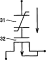
At first, with reference to Figure 16, in the FET type strong dielectric memory that uses in embodiment 8, memory cell 30 is made of strong dielectric electric capacity 31 and cell transistor 32.One end of strong dielectric electric capacity 31 is connected in word line WL, and the other end of strong dielectric electric capacity 31 is connected in the grid of cell transistor 32.FET type strong dielectric memory have following MFMIS (M: metal or conductor, F: strong dielectric, I: normal dielectric, S: structure semiconductor): between strong dielectric electric capacity 31 and Semiconductor substrate (not shown), the insertion conductive layer and be difficult to silicon dioxide (SiO
2) wait between the semiconductor the normal dielectric capacitance that forms the interface level.
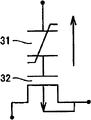
In embodiment illustrated in fig. 16 8 FET type strong dielectric memory, to establish Unit the 4th be selected cell, establish 1-Unit the 3rd is that non-selected cell describes.At this moment, establish by apply potential difference (PD) Vpp between the bit line BL1 of word line WL1 that selects and selection, as shown in figure 17, it is data [0] that the polarised direction of strong dielectric electric capacity 31 becomes downward state.In addition, establish that (Vpp), as shown in figure 18, it is the state of data [1] that the polarised direction of strong dielectric electric capacity 31 becomes the state of making progress by apply potential difference (PD) between the bit line BL1 of the word line WL1 that selects and selection.
Because apply with grid capacitance to strong dielectric electric capacity 31 and to carry out the voltage that electric capacity is cut apart, thus must set Vpp greatly, so that the polarized state of strong dielectric electric capacity 31 can fully be reversed.
Below, illustrate in the strong dielectric memory shown in Figure 16, prevent to remain on the method for operating of the data corruption in the non-selected cell.Because apply with grid capacitance to strong dielectric electric capacity 31 and to carry out the voltage that electric capacity is cut apart,, use high voltage Vpp so consider this point.In addition, in the explanation,, do not consider the depletion-layer capacitance of cell transistor 32 below in order to simplify.Under the situation of considering depletion-layer capacitance, cut apart as long as consider the electric capacity of the voltage that strong dielectric capacitance, grid capacitance and depletion-layer capacitance cause, adjust each voltage configuration and get final product.
(write activity)
At first, with reference to Figure 19 write activity when writing data [0] is described.
(1) opposite data write activity
As shown in figure 19, during (1) in, in selected cell (Unit the 4th), word line WL1 (select WL) be 0V, bit line BL1 (selecting BL) and source line SL1 (selection SL) become Vpp.Because substrate is connected with bit line, so near the current potential the substrate electric potential of cell transistor 32 and the semiconductor surface becomes Vpp.Apply with grid capacitance to the strong dielectric electric capacity 31 of selected cell (Unit the 4th) and to carry out voltage-Vcc that electric capacity is cut apart, write opposite data [1].Here, the voltage vcc that applies to strong dielectric electric capacity 31 uses grid capacitance Cg, strong dielectric capacitance Cf and voltage Vpp, is represented by following formula (4).
Vcc={Cg/(Cf+Cg)}Vpp…(4)
Therefore, as long as apply (Cf+Cg)/Cg voltage Vpp doubly of Vcc to memory cell.In addition, in Unit the 1st, apply 0V, apply 1/3Vpp, apply Vpp to source line SL1 (selecting SL) to bit line BL2 (non-selection BL) to word line WL1 (selecting WL) as non-selected cell.Near the substrate electric potential of the cell transistor 32 of Unit the 1st and the semiconductor surface current potential becomes 1/3Vpp, and the strong dielectric electric capacity 31 to Unit the 1st applies-potential difference (PD) of 1/3Vcc.In cell transistor shown in Figure 16 32, be under the situation of 1/3Vpp in the potential difference (PD) between word line and bit line, adjust threshold voltage, not form the tunnel.
In addition, in Unit the 2nd, apply 2/3Vpp, apply Vpp, apply 1/3Vpp to source line SL0 (non-selection SL) to bit line BL1 (selecting BL) to word line WL0 (non-selection WL) as non-selected cell.Near the substrate electric potential of Unit the 2nd and the semiconductor surface current potential becomes Vpp, and the strong dielectric electric capacity 31 to Unit the 2nd applies-potential difference (PD) of 1/3Vcc.
In addition, in Unit the 3rd, apply 2/3Vpp, apply the potential difference (PD) of 1/3Vpp to bit line BL2 (non-selection BL) and source line SL0 (non-selection SL) to word line WL0 (non-selection WL) as non-selected cell.Near the substrate electric potential of Unit the 3rd and the semiconductor surface current potential becomes 1/3Vpp, applies the potential difference (PD) of 1/3Vcc to the strong dielectric electric capacity 31 of Unit the 3rd.
(2) data write activity
In the Unit the 4th as selected cell, word line WL1 (selecting WL) is Vpp, and bit line BL1 (selecting BL), source line SL1 (selecting SL) become 0V.Because substrate is connected with bit line, so near the current potential the substrate electric potential of the cell transistor 32 of Unit the 4th (selected cell) and the semiconductor surface becomes 0V.Apply to the strong dielectric electric capacity 31 of Unit the 4th (selected cell) and to carry out the voltage vcc that electric capacity cuts apart with grid capacitance and (, write data [0] with reference to above-mentioned formula (4).
In addition, in Unit the 1st, apply Vpp, apply 2/3Vpp, apply 0V to source line SL1 (selecting SL) to bit line BL2 (non-selection BL) to word line WL1 (selecting WL) as non-selected cell.Near the substrate electric potential of the cell transistor 32 of Unit the 1st and the semiconductor surface current potential becomes 2/3Vpp, applies the potential difference (PD) of 1/3Vcc to the strong dielectric electric capacity 31 of Unit the 1st.
In addition, in Unit the 2nd, apply 1/3Vpp, apply 0V, apply 2/3Vpp to source line SL0 (non-selection SL) to bit line BL1 (selecting BL) to word line WL0 (non-selection WL) as non-selected cell.Near the substrate electric potential of Unit the 2nd and the semiconductor surface current potential becomes 0V, applies the potential difference (PD) of 1/3Vcc to the strong dielectric electric capacity 31 of Unit the 2nd.In addition, in Unit the 3rd, to word line WL0 (non-selection WL) when applying 1/3Vpp, apply the potential difference (PD) of 2/3Vpp to bit line BL2 (non-selection BL) and source line SL0 (non-selection SL) as non-selected cell.Near the substrate electric potential of Unit the 3rd and the semiconductor surface current potential becomes 2/3Vpp, and the strong dielectric electric capacity 31 to Unit the 3rd applies-potential difference (PD) of 1/3Vcc.
By the opposite data write activity of Figure 19 (1) and the data write activity of (2), apply ± 1/3Vcc to the strong dielectric electric capacity 31 of non-selected cell (unit, the 1st unit-the 3rd).Therefore, by using voltage configuration shown in Figure 19, disturb the data corruption of the non-selected cell that causes in the time that write activity can being suppressed.
Write at Figure 20 under the situation of data [1], only replace action during (1) that writes under data [0] situation shown in Figure 19 and the action during (2), other action is identical with the situation that writes data [0].
(read/write activity) again
Reading/writing again in the configuration of fashionable voltage, as shown in figure 21, be divided into that read (1), (2) [1] writes, (3) [1] writes, (4) [0] writes (reading again) these 4 actions more again.And, keeping at memory cell under the situation of data [1], action finishes in (2), under the situation that keeps data [0], moves, up to (4).
(1) reads action
At first, reading of data by between the bit line BL1 of word line WL1 that selects (selecting WL) and selection (selecting BL), applying potential difference (PD) Vpp, simultaneously, apply appropriate voltage to the source line SL1 that selects (selecting SL), the drain current of determination unit transistor 23 carries out.But by measuring the reasons are as follows of drain current judgment data.That is, in selected cell, keep under the situation of data [1], when reading, because the counter-rotating of the polarized state of strong dielectric electric capacity 31, so fully big quantity of electric charge Qg takes place in the grid of cell transistor 32.Simultaneously, near the electric charge of the generation-Qg semiconductor surface under the grid of cell transistor 32.Thereby the conducting owing to the counter-rotating electronics between source, drain electrode is so flow through drain current.
On the other hand, under the situation that keeps data [0], when reading, because the polarized state of strong dielectric electric capacity 31 is nonreversible, so under the abundant big situation of selecting between WL and the selection BL of potential difference (PD) Vpp, electric charge does not take place substantially in the grid of cell transistor 23 yet.Therefore because do not respond to negative charge near the semiconductor surface under the grid substantially yet, so the source of cell transistor 32, the drain electrode between not conducting.Therefore, do not flow through drain current.So can come judgment data by measuring drain current.
Particularly, as shown in figure 21,, in Unit the 4th, apply Vpp, apply 0V, apply Vpp to source line SL1 (selecting SL) to bit line BL1 (selecting BL) to word line WL1 (selecting WL) as selected cell reading in the action of (1).Because substrate is connected with bit line, so the substrate electric potential of the cell transistor 32 of Unit the 4th becomes 0V.Under the situation that keeps data [1], the counter-rotating of the polarized state of the strong dielectric electric capacity 31 of Unit the 4th (selected cell).Thereby,, form the tunnel because big electric charge takes place on grid.Therefore, in the cell transistor 32 of Unit the 4th (selected cell), flow through drain current.On the other hand, under the situation that keeps data [0], the polarized state of the strong dielectric electric capacity 31 of Unit the 4th (selected cell) is nonreversible.Therefore, owing in the cell transistor 32 of Unit the 4th (selected cell), do not form the tunnel, so do not flow through drain current.By measuring drain current, judgment data [0] and [1].
In addition, in Unit the 1st, apply Vpp, apply 2/3Vpp, apply Vpp to source line SL1 (selecting SL) to bit line BL2 (non-selection BL) to word line WL1 (selecting WL) as non-selected cell.Near the substrate electric potential of the cell transistor 32 of Unit the 1st and the semiconductor surface current potential becomes 2/3Vpp, applies the potential difference (PD) of 1/3Vcc to the strong dielectric electric capacity 31 of Unit the 1st.
In addition, in Unit the 2nd, apply 1/3Vpp, apply 0V, apply 2/3Vpp to source line SL0 (non-selection SL) to bit line BL1 (selecting BL) to word line WL0 (non-selection WL) as non-selected cell.Near the substrate electric potential of Unit the 2nd and the semiconductor surface current potential becomes 0V, applies the potential difference (PD) of 1/3Vcc to the strong dielectric electric capacity 31 of Unit the 2nd.In addition, in Unit the 3rd, apply 1/3Vpp, apply the potential difference (PD) of 2/3Vpp to bit line BL2 (non-selection BL) and source line SL0 (non-selection SL) to word line WL0 (non-selection WL) as non-selected cell.Near the substrate electric potential of Unit the 3rd and the semiconductor surface current potential becomes 2/3Vpp, and the strong dielectric electric capacity 31 to Unit the 3rd applies-potential difference (PD) of 1/3Vcc.
(2) data [1] write activity again
The opposite data of carrying out in during (1) when the voltage of this moment disposes with data shown in Figure 19 [0] write activity write identical.Keep reading under the situation of data [1] in the Unit the 4th as selected cell/write activity here finishes again.
(3) data [1] write activity
The opposite data of carrying out in during (1) when the voltage of this moment disposes with data shown in Figure 19 [0] write activity write identical.
(4) data [0] write (reading again) action again
Reading of carrying out in during (1) of the write activity of the voltage configuration of this moment and shown in Figure 21 reading/again is identical.That is, to selecting WL to apply Vpp, to selecting BL to apply 0V, to selecting SL to apply Vpp.
At this moment, can not apply Vpp yet, and apply 0V to selection SL.Particularly, in the data [0] of (4) again under the write state, in the data of (3) [1] write activity for writing the state of data [1], so must apply voltage to strong dielectric electric capacity 31 along the polarization reversal direction as Unit the 4th of selected cell.Therefore, under cell transistor 32 grids, form the tunnel.At this moment, if as mentioned above to selecting SL to apply Vpp, then near the current potential the semiconductor surface under the 4th cell gate may not become and select the identical current potential (0V) of bit line BL1, so do not limit the potential difference (PD) that applies Vcc to strong dielectric electric capacity 31.On the contrary, be 0V if select source line SL1, even then form the tunnel, near the current potential the semiconductor surface also can be changed into 0V, can write data [0] really.Selection source line SL1 is that the data of carrying out in during (2) during with [0] shown in Figure 19 data write activity as the action of 1-Unit the 3rd of non-selected cell under the 0V situation write identical.
In embodiment 8, by the write activity of the reading of (1)-(4)/again, apply ± 1/3Vcc with the strong dielectric electric capacity 31 of same number respectively, so disturb the data corruption of the non-selected cell that causes can suppress write activity the time to non-selected cell (unit, the 1st unit-the 3rd).
(embodiment 9)
With reference to Figure 22, illustrate that 1-8 is different with the foregoing description in embodiment 9, apply the 1/2Vcc voltage condition to non-selected cell.
Particularly, in the strong dielectric memory of the simple matrix mode of embodiment 9, as shown in figure 22, the 1/3Vcc2/3Vcc generative circuit 10 of the strong dielectric memory with embodiment illustrated in fig. 11 replaces to 1/2Vcc generative circuit 10a.Other structure is the same with embodiment illustrated in fig. 11.
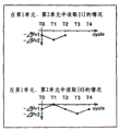
With reference to Figure 23 and Figure 24, illustrate among the embodiment 9, will be positioned at Unit the 4th on word line WL3 shown in Figure 23 and the bit line BL3 intersection point as selected cell.The voltage waveform that is applied on word line WL and the bit line BL shown in Figure 24.If time of each action of T1 shown in Figure 24 (1), T2 (2), T3 (3) and T4 (4) is (T second: same pulse width) identical time.In addition, each action of (1)-(4) both can from (1) to (4) be carried out continuously, also can independently carry out respectively.Below, illustrate (1)-each action in (4).Under waiting status, establishing word line WL and bit line BL is 0V.
(1) reads action T1
Read action in during T1 shown in Figure 24.At first, select BL to become quick condition (high impedance status) from waiting status.Under identical timing or make constant time lag count the tens of nsec of nsec-, select WL to become Vcc, non-selection WL becomes 1/2Vcc.Select BL become 0V thereafter.When selecting BL to be quick condition,, carry out the judgement of data [0] or data [1] by detecting the voltage of selecting BL.By by as the read-out amplifier 8 (with reference to Figure 22) of voltage sensor amplifier relatively and amplify the current potential of selecting BL and generate in addition with reference to current potential, carry out the judgement of data [0] or [1].
Reading in the action of T1, in being connected in Unit the 2nd of selecting the non-selected cell of conduct on the BL, as shown in figure 25, t1 (<apply the 1/2Vcc-Vr potential difference (PD) during T1), afterwards, during (T1-t1), apply the potential difference (PD) of 1/2Vcc.In addition, to being connected in Unit the 1st of selecting the non-selected cell of conduct on the WL, during T1, apply the potential difference (PD) of 1/2Vcc.In addition, to not being connected in Unit the 3rd of selecting WL and selecting the non-selected cell of conduct on the BL, during T1, apply 0V.On the other hand, the Unit the 4th to as selected cell applies the Vcc-Vr potential difference (PD) during t1, afterwards, applies the potential difference (PD) of Vcc during (T1-t1).
In embodiment 9, in being connected in Unit the 2nd of selecting the non-selected cell of conduct on the BL, will set fully shortly during the t1, the amount of polarization changes delta Pr that (1/2Vcc-Vr) that accept during the t1 caused
aThe amount of polarization changes delta Pr that causes with the 1/2Vcc that accepts during (T1-t1) is than fully little, and, Δ Pr become with during T1 after T2-T4 in the amount of polarization that takes place respectively change essentially identical amount.
As a result, in being connected in Unit the 2nd of selecting the non-selected cell of conduct on the BL, in the memory cell that keeps data [1], as shown in figure 26, produce the deterioration of polarized state, in the memory cell that keeps data [0], as shown in figure 27, produce the improvement of polarized state.In being connected in the non-selected cell of selecting on the WL (Unit the 1st), in the memory cell that keeps data [1], as shown in figure 28, produce the deterioration of polarized state, in the memory cell that keeps data [0], as shown in figure 29, produce the improvement of polarized state.Be connected on non-selection WL and the non-selection BL non-selected cell (Unit the 3rd) since in during the T1 potential difference (PD) be 0V, so with the data independence that keeps, polarized state does not change (not shown).In addition, in the Unit the 4th as selected cell, under the situation that keeps data [1], as shown in figure 30, data [1] are destroyed, become the state that writes data [0].In addition, keep at selected cell (Unit the 4th) under the situation of data [0], as shown in figure 31, data are not destroyed.
(2) write activity T2 again
Above-mentioned (1) read action after, as shown in figure 24, temporarily return waiting status.Afterwards, select WL to become 0V, non-selection WL becomes 1/2Vcc, selects BL to become Vcc, and non-selection BL becomes 1/2Vcc.During write activity T2 again, the Unit the 1st and the Unit the 2nd that apply the non-selected cell of conduct of 1/2Vcc during the T1 that is reading action apply-1/2Vcc.In addition, apply 0V to Unit the 3rd of the non-selected cell of conduct that during T1, applies 0V once more.
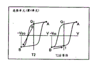
As a result, in as Unit the 1st of non-selected cell and Unit the 2nd, keep in the situation of data [1], as shown in figure 33, produce the improvement of polarized state.In Unit the 1st and Unit the 2nd, keep in the situation of data [0], as shown in figure 34, produce the deterioration of polarized state.Be connected on non-selection WL and the non-selection BL non-selected cell (Unit the 3rd) since in during the T2 potential difference (PD) be 0V, so with the data independence that keeps, polarized state does not change (not shown).In addition, in Unit the 4th, as shown in figure 35, write data [1] as selected cell.(1) read the action T1 in, under the situation of reading of data [1], embodiment 9 read and again write activity finish at T2.
(3) compensating movement T3
Behind the T2 of write activity again of above-mentioned (2), as shown in figure 24, temporarily return waiting status.Afterwards, select WL to become 0V once more, non-selection WL becomes 1/2Vcc, selects BL to become Vcc, and non-selection BL becomes 1/2Vcc.In write activity T2 again, as shown in figure 36, once more to apply-the non-selected cell (Unit the 1st and Unit the 2nd) of 1/2Vcc applies-1/2Vcc.In addition, in write activity T2 again, the non-selected cell (Unit the 3rd) that applies 0V is still constant for 0V.
As a result, in Unit the 1st and Unit the 2nd, keep in the situation of data [1], as shown in figure 37, produce the improvement of polarized state.In Unit the 1st and Unit the 2nd, keep in the situation of data [0], as shown in figure 38, produce the deterioration of polarized state.Among Figure 38, the reduction of the amount of polarization when Δ Pr represents twice deterioration of polarized state.In addition, in Unit the 3rd, because potential difference (PD) is 0V, so polarized state does not change (not shown) as non-selected cell.In addition, in Unit the 4th, as shown in figure 39, write data [1] once more as selected cell.
(4) write activity T4 again
Behind the compensating movement T3 of above-mentioned (3), as shown in figure 24, temporarily return waiting status.Afterwards, select WL to become Vcc, non-selection WL becomes 1/2Vcc, selects BL to become 0V, and non-selection BL becomes 1/2Vcc.In write activity T4 again, as shown in figure 40, in compensating movement T3, apply-the non-selected cell (Unit the 1st and Unit the 2nd) of 1/2Vcc applies 1/2Vcc.On the other hand, the non-selected cell (Unit the 3rd) that applies 0V in compensating movement T3 is still constant for 0V.
As a result, in Unit the 1st and Unit the 2nd, keep in the situation of data [1], as shown in figure 41, produce the deterioration of polarized state.In Unit the 1st and Unit the 2nd, keep in the situation of data [0], as shown in figure 42, produce the improvement of polarized state.On the other hand, in Unit the 3rd, because potential difference (PD) is 0V, so polarized state does not change (not shown) as non-selected cell.In addition, in Unit the 4th, as shown in figure 43, write data [0] as selected cell.
Here, in embodiment 9, the polarized state of the memory cell under the waiting status behind waiting status behind the T2 of write activity more shown in Figure 32 or the T4 of write activity more shown in Figure 40 becomes a series of reading and the polarized state of each memory cell behind the write activity again.In the partial memory unit, the deterioration of the polarized state that causes takes place once to disturb.But, repeating to read and again under the situation of write activity, the deterioration of polarized state can not increase yet.
Original state (T0) beginning of never disturbing the polarized state cause to worsen shown in Figure 44, carry out embodiment 9 read and again under the write activity situation amount of polarization of Unit the 1st and Unit the 2nd change.In addition, the original state (T0) from once disturbing the polarized state cause to worsen shown in Figure 45 is carried out reading and the amount of polarization variation of Unit the 1st and Unit the 2nd under the write activity situation again of embodiment 9.As Unit the 3rd of non-selected cell a series of read and again during write activity potential difference (PD) always be 0V, polarized state does not change (not disturbing), so not shown.As Figure 44 and shown in Figure 45, repeating to read and again under the situation of write activity, the deterioration of polarized state can not increase yet as can be known.
In embodiment 9, as mentioned above, by reading action and write activity again, apply alternately ± 1/2Vcc by the Unit the 1st in non-selected cell and Unit the 2nd, can effectively suppress the data corruption that polarized state worsens the non-selected cell (Unit the 1st and Unit the 2nd) that causes.In addition, in the Unit the 3rd in non-selected cell,, always apply 0V, so can not produce the data corruption that polarized state worsens the non-selected cell that causes by reading action and write activity again.
(write activity)
Below, with reference to Figure 46-Figure 54, the write activity of the data [1] in the strong dielectric memory of simple matrix mode of embodiment 9 is described.
(1) compensating movement T1
At first, as shown in figure 46, select WL to become Vcc from waiting status, non-selection WL becomes 1/2Vcc from waiting status, selects BL to become 0V from waiting status, and non-selection BL becomes 1/2Vcc from waiting status.At this moment, the potential difference (PD) that applies to each memory cell becomes as shown in figure 47.That is, apply 1/2Vcc, apply 0V in the Unit the 3rd in non-selected cell during the T1 in the Unit the 1st in non-selected cell and Unit the 2nd during the T1.On the other hand, during T1 to the potential difference (PD) that applies Vcc as Unit the 4th of selected cell.
As a result, in Unit the 1st and Unit the 2nd, keep in the situation of data [1], as shown in figure 48, produce the deterioration of polarized state.In as Unit the 1st of non-selected cell and Unit the 2nd, keep in the situation of data [0], as shown in figure 49, produce the improvement of polarized state.In addition, in Unit the 3rd, because potential difference (PD) is 0V, so polarized state does not change (not shown) as non-selected cell.In addition, in Unit the 4th, as shown in figure 50, write data [0] as selected cell.
(2) write activity T2
During write activity T2, as shown in figure 46, select WL to become 0V from waiting status, non-selection WL becomes 1/2Vcc from waiting status, selects BL to become Vcc from waiting status, and non-selection BL becomes 1/2Vcc from waiting status.At this moment, the potential difference (PD) that applies to each memory cell becomes shown in Figure 51.That is, apply-1/2Vcc in the Unit the 1st in non-selected cell and Unit the 2nd during the T2.In addition, apply the potential difference (PD) of 0V in the Unit the 3rd in non-selected cell during the T2.On the other hand, during T2, apply-potential difference (PD) of Vcc to Unit the 4th as selected cell.
As a result, in as Unit the 1st of non-selected cell and Unit the 2nd, keep in the situation of data [1], shown in Figure 52, produce the improvement of polarized state.Keep in the situation of data [0] in Unit the 1st in non-selected cell and the Unit the 2nd, produce the deterioration of polarized state.In addition, in the Unit the 3rd in non-selected cell, because potential difference (PD) is 0V, so polarized state does not change (not shown).In addition, in Unit the 4th, shown in Figure 54, write data [1] as selected cell.
The polarized state of each memory cell becomes the polarized state of each memory cell behind a series of write activities under the waiting status shown in Figure 52-Figure 54 behind the T2.In the partial memory unit, the deterioration of the polarized state that causes takes place once to disturb.But under the situation that repeats write activity, the deterioration of polarized state can not increase yet.In embodiment 9, in a series of write activities, because the deterioration of polarized state and improvement respectively cause once respectively, so once disturb the original state that causes that polarized state worsens from existing, under the situation of a series of write activities of beginning, finish the back deterioration amount at write activity and also can not increase.
In the write activity of data [0], also the write activity with above-mentioned data [1] is the same, after writing opposite data in advance, writes the data that should write.This moment, the effect of gained was the same with the above-mentioned effect of data [1].
In embodiment 9, as mentioned above, because drive word line WL and bit line BL,, can reduce the voltage kind so compare with the foregoing description 1-8 that drives word line WL and bit line BL with Vcc, 2/3Vcc, 1/3Vcc and 0V4 kind voltage with Vcc, 1/2Vcc and 0V3 kind voltage.Thereby, in embodiment 9, compare, but simplified control circuit simultaneously, reduces consumed power, and voltage generation circuit is become simple with embodiment 1-8.
In addition, in the foregoing description 9, set Vcc, make the reactance voltage of considering less than the hysteresis characteristic that has from the memory cell that constitutes strong dielectric memory as the 1/2Vcc that is applied to the magnitude of voltage on the non-selected cell (polarization reversal voltage).Thus, can reduce the deterioration amount that finally occurs in the polarized state in the non-selected cell.
Current disclosed embodiment is example in all respects, should think and limiting examples.Scope of the present invention can't help the foregoing description explanation and represent by the claim scope, and comprise and the implication of claim scope equalization and all changes in the scope.
For example, in the above-described embodiments, between each action (1)-(4), dispose waiting status, but the invention is not restricted to this, also can move and not dispose waiting status between (1)-(4), and carry out continuously at each.
In the above-described embodiments, the strong dielectric memory that comprises strong dielectric film as memory unit is described, but the invention is not restricted to this, so long as memory unit is connected the storer between bit line and the word line, also other storer.For example, though the storer that forms by resistive element for memory unit, also can be suitable equally.
In addition, in the foregoing description 8,, the invention is not restricted to this, even also can be suitable equally for FET type strong dielectric memory with MFIS structure and MFS structure though understand FET type strong dielectric memory with MFMIS structure.
In addition, in the foregoing description 8, that is reading/carrying out during (1) of write activity reads in the action, to the voltage that applies Vpp as the source line SL1 (selecting SL) of Unit the 4th of selected cell, but the invention is not restricted to this, for example also can be to selecting SL to apply identical voltages such as 2/3Vpp with non-selection BL.
In addition, in the above-described embodiments, though illustrate (1)-each actuation time of (4) is the example of identical time (T second), but the invention is not restricted to this, for example during with (1), be made as T1 second, will be made as T2 second during (2), repeat under the situation of (1) and (2), as long as not taking place in fact in the non-selected cell, polarized state worsens, also T1 ≠ T2.
In addition, in the above-described embodiments, be illustrated in that word line WL and bit line BL are the example of 0V under the waiting status, but the invention is not restricted to this, word line WL and bit line BL also can be the regulation same potential beyond the 0V under waiting status.For example, establishing under the voltage condition of WL=BL=1V as waiting status, when reading, as what is called selection BL=1V → floating, the current potential before selection BL floats must become the current potential of waiting status.
In the above-described embodiments, when data read, to select WL, non-selection WL and non-selection BL to be set at assigned voltage to become the identical timing of quick condition from waiting status with selection BL, but the invention is not restricted to this, also can will select WL, non-selection WL and non-selection BL to be set at assigned voltage from selecting BL become the timing that quick condition postpones tens of nsec from waiting status.
In addition, in embodiment illustrated in fig. 41, the example that the voltage of waiting status is made as WL=BL=0V is shown, but the invention is not restricted to this, also can be as the variation 1 of Figure 55 illustrated embodiment 1, the voltage of waiting status is made as WL=BL=Vcc.The voltage configuration of this moment is shown in Figure 55.At this moment, under the situation that reads reading of data in the action [0] of (1), in the action of (2), stop, under the situation that reads reading of data in the action [1] of (1), proceed to the action of (4).Even in the variation 1 of embodiment 1, also the same with the foregoing description 1, under two kinds of situations of situation of the situation of reading of data [1] and reading of data [0], the number of times that improves of the deterioration number of times of polarized state and polarized state equates.Therefore, even repeat to read action and write activity again, the deterioration that yet can not accumulate polarized state in the non-selected cell finally can not destroy the data of maintenance.Voltage in waiting status is under the situation of WL=BL 〉=1/2Vcc, and the order of the variation 1 of Figure 55 illustrated embodiment 1 preferably is under the situation of WL=BL<1/2Vcc at the voltage of waiting status, preferably embodiment illustrated in fig. 41 order.
In addition, in embodiment illustrated in fig. 41, in the data that read is under the situation (situation of [1] Read) of [1], though only in (1) and (2), finish to read action and write activity again, but the invention is not restricted to this, also can be as the variation 2 and the variation 3 of Figure 56 and Figure 57 illustrated embodiment 1, under the situation (situation of [1] Read) of [1], under the order of (1)-(4), read action and write activity again in the data that read.At this moment, in the data that read is under the situation (situation of [1] Read) of [1], under the order of (1) shown in Figure 56 or Figure 57-(4), read action and write activity, for under the situation (situation of [0] Read) of [0], under the order of (1) shown in Figure 4-(4), read action and write activity in the data that read.