CN100426505C - Differential capacitor, differential antenna element, and differential resonator - Google Patents
Differential capacitor, differential antenna element, and differential resonator Download PDFInfo
- Publication number
- CN100426505C CN100426505C CNB200410062884XA CN200410062884A CN100426505C CN 100426505 C CN100426505 C CN 100426505C CN B200410062884X A CNB200410062884X A CN B200410062884XA CN 200410062884 A CN200410062884 A CN 200410062884A CN 100426505 C CN100426505 C CN 100426505C
- Authority
- CN
- China
- Prior art keywords
- barricade
- capacitor
- differential
- vertical plane
- diffferential
- Prior art date
- Legal status (The legal status is an assumption and is not a legal conclusion. Google has not performed a legal analysis and makes no representation as to the accuracy of the status listed.)
- Expired - Fee Related
Links
Images


Classifications
-
- H—ELECTRICITY
- H01—ELECTRIC ELEMENTS
- H01L—SEMICONDUCTOR DEVICES NOT COVERED BY CLASS H10
- H01L23/00—Details of semiconductor or other solid state devices
- H01L23/52—Arrangements for conducting electric current within the device in operation from one component to another, i.e. interconnections, e.g. wires, lead frames
- H01L23/522—Arrangements for conducting electric current within the device in operation from one component to another, i.e. interconnections, e.g. wires, lead frames including external interconnections consisting of a multilayer structure of conductive and insulating layers inseparably formed on the semiconductor body
- H01L23/5222—Capacitive arrangements or effects of, or between wiring layers
- H01L23/5223—Capacitor integral with wiring layers
-
- H—ELECTRICITY
- H01—ELECTRIC ELEMENTS
- H01P—WAVEGUIDES; RESONATORS, LINES, OR OTHER DEVICES OF THE WAVEGUIDE TYPE
- H01P1/00—Auxiliary devices
- H01P1/20—Frequency-selective devices, e.g. filters
- H01P1/201—Filters for transverse electromagnetic waves
- H01P1/203—Strip line filters
-
- H—ELECTRICITY
- H01—ELECTRIC ELEMENTS
- H01Q—ANTENNAS, i.e. RADIO AERIALS
- H01Q1/00—Details of, or arrangements associated with, antennas
- H01Q1/52—Means for reducing coupling between antennas; Means for reducing coupling between an antenna and another structure
- H01Q1/526—Electromagnetic shields
-
- H—ELECTRICITY
- H01—ELECTRIC ELEMENTS
- H01Q—ANTENNAS, i.e. RADIO AERIALS
- H01Q15/00—Devices for reflection, refraction, diffraction or polarisation of waves radiated from an antenna, e.g. quasi-optical devices
- H01Q15/0006—Devices acting selectively as reflecting surface, as diffracting or as refracting device, e.g. frequency filtering or angular spatial filtering devices
- H01Q15/0013—Devices acting selectively as reflecting surface, as diffracting or as refracting device, e.g. frequency filtering or angular spatial filtering devices said selective devices working as frequency-selective reflecting surfaces, e.g. FSS, dichroic plates, surfaces being partly transmissive and reflective
-
- H—ELECTRICITY
- H01—ELECTRIC ELEMENTS
- H01Q—ANTENNAS, i.e. RADIO AERIALS
- H01Q23/00—Antennas with active circuits or circuit elements integrated within them or attached to them
-
- H—ELECTRICITY
- H01—ELECTRIC ELEMENTS
- H01L—SEMICONDUCTOR DEVICES NOT COVERED BY CLASS H10
- H01L2924/00—Indexing scheme for arrangements or methods for connecting or disconnecting semiconductor or solid-state bodies as covered by H01L24/00
- H01L2924/0001—Technical content checked by a classifier
- H01L2924/0002—Not covered by any one of groups H01L24/00, H01L24/00 and H01L2224/00
-
- H—ELECTRICITY
- H01—ELECTRIC ELEMENTS
- H01L—SEMICONDUCTOR DEVICES NOT COVERED BY CLASS H10
- H01L2924/00—Indexing scheme for arrangements or methods for connecting or disconnecting semiconductor or solid-state bodies as covered by H01L24/00
- H01L2924/30—Technical effects
- H01L2924/301—Electrical effects
- H01L2924/3011—Impedance
Abstract
In a differential capacitor (1), first and second capacitors (1003 and 1004) are formed in substantially symmetrical positions from each other with respect to a vertical plane (B-B'), on a semiconductor substrate (1020). The differential capacitor (1) further includes a shield plate (1022) interposed between the semiconductor substrate (1020) and the lower electrodes (1016 and 1018). When each of the lower electrodes (1016 and 1018) is proj ected onto the shield plate (1022) along the vertical direction, each projected lower electrode (1016 or 1018) has a partial overlap with the shield plate (1022).
Description
Technical field
The present invention relates to diffferential capacitor, differential antenna element and differential resonator.More particularly, the present invention relates to the diffferential capacitor, differential antenna element and the differential resonator that on the semiconductor-based end, form.
Background technology
In recent years, proposed towards the semiconductor process techniques of miniaturization and higher-frequency more, just because of this reason will become usual thing by integrated differential oscillating circuit on semiconductor.Figure 17 is the structural representation that differential oscillating circuit 7 is used in explanation usually.In Figure 17, this differential oscillating circuit 7 comprises: first and second transistors 1001 and 1002 that are used to start vibration; First and second capacitors 1003 and 1004 that are used to form diffferential capacitor and end DC (direct current) component; Be used to start first and second variable capacitors 1005 and 1006 of resonance; Be used to start first and second inductors 1007 and 1008 of resonance; And constant current supply 1009.
By the Vcc terminal, the DC electric current is applied to the one the second inductors 1007 and 1008 of this differential oscillating circuit 7.This DC electric current is applied to first transistor seconds 1001 and 1002, and the constant current supply 1009 of after this just flowing through is to ground.Connect the first transistor and make the realization positive feedback, and produce the right in-phase signal of composition differential wave or any one signal in the inversion signal, this signal has the frequency of oscillation according to the circuit constant of first variable capacitor 1005 and first inductor 1007.The transistor seconds 1002 that is similar to the first transistor 1001 work produce and inversion signal respectively from Vo
+Terminal and Vo
-Terminal output, perhaps vice versa.
But, in above-mentioned differential oscillating circuit 7, the parasitic capacitance Cpa that links and the influence of dead resistance Rpa (being shown in broken lines) are arranged in Figure 17, when frequency of oscillation improves and increase with first capacitor 1003.The result is that the sharpness of resonance that is caused by first variable capacitor 1005 and first inductor 1007 degenerates; In other words, quality factor (it is used as an index of the sharpness of resonance) degenerate.The resonance that is caused by second variable capacitor 1006 and second inductor 1008 also is subjected to similarly degenerate.Figure 18 A illustrates the last plane graph that is integrated in the suprabasil diffferential capacitor structure of semiconductor (first capacitor 1003 and second capacitor 1004).Figure 18 B takes from along first capacitor 1003 of the vertical plane A-A ' that is shown in Figure 18 A and the cross-sectional view of second capacitor 1004.In Figure 18 A and 18B, first capacitor 1003 and second capacitor 1004 are formed in the interlayer film 1019 at the semiconductor-based end 1020, and this substrate normally is made up of p type silicon.Interlayer film 1019 normally is made up of silicon dioxide.More precisely, first capacitor 1003 comprises the normally top electrode 1015 and the bottom electrode 1016 of the wirework composition of aluminium.Top electrode 1015 and bottom electrode 1016 are disposing with predetermined interval in parallel with each other along vertical direction.Second capacitor 1004 is by forming with first capacitor, 1003 identical materials, and comprises top electrode 1017 and bottom electrode 1018, and this a pair of electrode is with respect to predetermined vertical plane B-B ', divides to take leave of the position of top electrode 1015 and bottom electrode 1016 symmetries and form.
In order to suppress this dead resistance, following diffferential capacitor (being referred to as " conventional diffferential capacitor " hereinafter) has been proposed.Figure 19 A is the upper plane view that this constant diffferential capacitor structure schematically is shown.Figure 19 B takes from along the vertical plane A-A ' that is shown in Figure 19 A to locate the cross-sectional view of first capacitor 1003 and second capacitor 1004.The conventional diffferential capacitor that is shown in Figure 19 A and 19B has comprised additional barricade 1021, has any different with the capacitor that is shown in Fig. 1 gA and 18B in this.In others, these two diffferential capacitors are identical.So in Figure 19 A and 19B, those have the part element of their homologue to point out by adopting used therein those identical reference numbers in Figure 18 A and 18B, and omit description of them.
Barricade 1021 is configured between the semiconductor-based end 1020 and bottom electrode 1016 and 1018, and this plate is by the parts of forming such as the electric conducting material of aluminium that resemble plate one spline structure.More precisely, this barricade has such shape, makes that the bottom electrode 1016 and 1018 that is projected looks as if is included in the outer outline of barricade 1012 when bottom electrode 1016 and 1018 is vertically projected to barricade from above.Barricade 1021 has the symmetric shape with respect to above-mentioned vertical plane B-B '.Have barricade 1021 like this, though the parasitic capacitance in interlayer film 1019 is enhanced, the dead resistance in the semiconductor-based end 1020 is lowered.
By the differential oscillating circuit 7 of conventional differential capacitance structure applications, can improve the middle sharpness of resonance that each resonator circuit produces to diagrammatic sketch 17.Say exactly, shown in the equivalent circuit among Figure 20, following parasitic component will appear in the differential oscillating circuit 7: the parasitic capacitance Cpa1 between bottom electrode 1016 and barricade 1021, at bottom electrode 1018 and the parasitic capacitance Cpc at the semiconductor-based end, and the dead resistance Rpc in the semiconductor-based end 1020.Because in-phase signal and inversion signal are applied to first capacitor 1013 and second capacitor 1004 (or vice versa), the knot between parasitic capacitance Cpa1 and Cpa2 plays a part the apparent ground connection (being referred to as " virtual ground " hereinafter) with respect to the AC signal.The result is can reduce parasitic capacitance Cpc and post the influence of resistance R pc to resonator circuit.
But, if conventional diffferential capacitor structure is applied to differential oscillating circuit 7, parasitic capacitance Cpa1 and Cpa2 (seeing Figure 20) in fact just will not be connected in parallel with first variable capacitor 1015 and second variable capacitor 1016 for those.And, because parasitic capacitance Cpa1 and Cpa2 have fixing value, so the capacitance variations value in first variable capacitor 1005 and second variable capacitor 1006 will become littler than they specification value separately, therefore cause narrowing down at the surge frequency range of differential oscillating circuit 7.
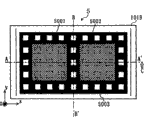
Simultaneously, integrated differential antenna element has also become usual thing on semiconductor.Figure 21 is the structure perspective view that conventional plane differential antenna element 7001 is shown.Be shown in the planar antenna element 7001 of Figure 21 at this, it is identical but have an in-phase signal and an inversion signal of 180 ° of phase differences that two planar antenna elements 7002 and 7003 outputs have power to each other, these two antenna elements with predetermined arranged spaced separated from one another on silicon base 7004.The result is that this differential antenna element 7001 can receive wide band signal.
But, when planar antenna element 7002 and 7003 is formed on the silicon base 7004, will cause following point: because coupling has taken place the parasitic capacitance between wiring and silicon base 7004; And because loss has taken place in the dead resistance influence at the semiconductor-based end 7004.The result is that the gain of differential antenna element 7001 will degenerate.
Figure 22 is the schematic diagram that illustrates in conjunction with balance high-frequency element 8001 structures of conventional differential resonator.In Figure 22, this balance high-frequency element 8001 comprises: the input IN that is used for receiving inputted signal; Balancing device 8002 with output OUT1 and OUT2 is from this two output output in-phase signals and inversion signal; And half-wave resonator 8003 (as the example of differential resonator).When reception has the signal of preset frequency, this 1/2 wave resonator is made resonance so that reduce the impedance of this in-phase signal component, this impedance exists when balancing device 8,002 one sides are watched output, thereby, must than when the impedance of the differential signal component that when these balancing device 8,002 one sides are watched this output, exists low.Therefore, this balance high-frequency element 8001 has suppressed this same phase component, and has improved the balanced degree between output signal.
But, when going up formation 1/2 wave resonator 8003 in silicon base (as the example at the semiconductor-based end), the problem below will causing: because coupling has taken place the parasitic capacitance between 1/2 wave resonator 8003 and silicon base; And, because loss has taken place in the influence of the dead resistance in the semiconductor-based end.The result is to increase the insertion loss of 1/2 wave resonator 8003.
Summary of the invention
Therefore, first purpose of the present invention provides and a kind ofly can be on differential oscillating circuit be kept to minimum diffferential capacitor to parasitic capacitance and dead resistance.
Second purpose of the present invention provides and a kind ofly can be kept to minimum differential antenna element to parasitic capacitance and dead resistance.
The 3rd purpose of the present invention provides and a kind ofly can be kept to minimum differential resonator to parasitic capacitance and dead resistance.
In order to obtain the first top purpose, a first aspect of the present invention is to comprise the diffferential capacitor of a plurality of capacitors, each capacitor has along vertical direction top electrode and bottom electrode parallel to each other basically, arbitrary capacitor is formed on the position with respect to another basic symmetry of vertical plane in a plurality of capacitors at semiconductor-based the end in wherein a plurality of capacitors, this diffferential capacitor also comprises each bottom electrode of insertion and the barricade at the semiconductor-based end, and when each bottom electrode when vertical direction is projected to barricade, bottom electrode that respectively is projected and barricade have overlaps.The result is, becoming might provide a kind of can reduce the parasitic capacitance of itself and the diffferential capacitor of dead resistance on differential oscillating circuit.
Preferably, the overlapping of bottom electrode that respectively is projected and barricade account for altogether the bottom electrode area 70% or more.As preferable example, the bottom electrode that respectively is projected extends in the outside of barricade.As another preferred embodiments, barricade has the elongated breach that is formed on wherein.More preferably, this elongated breach and this vertical plane intersect.
Preferably, barricade has a plurality of apertures that run through that are formed on wherein.As preferable example, these are a plurality of to run through apertures with the interval that equates basically, along two predetermined directions configurations, and is the integral multiple that is substantially equal to 1/2 wavelength of the standing wave propagated through this barricade at interval between a plurality of two apertures that run through in the aperture that adjoin.More preferably, the length from two of barricade predetermined sides to this vertical plane is to be substantially equal to the integral multiple of 1/2 wavelength of this standing wave and 1/4 wavelength sum of standing wave.
Preferably, between a plurality of capacitors, any two capacitors that adjoin each other receive respectively forms differential right in-phase signal of signal and inversion signal.
Preferably, this barricade is by inductor and/or resistance-grounded system.As another preferred embodiments, the part of the barricade that intersects with this vertical plane is a ground connection.
Preferably, this diffferential capacitor is used for variable capacitance circuit, and at least one variable capacitor is linked to each bottom electrode or at least one variable capacitor is linked to each top electrode in this circuit.The area of overlapping of bottom electrode that more preferably, respectively is projected and barricade is determined according to the rate of change of capacitance of variable capacitance circuit and the quality factor of each capacitor.
As an example, this diffferential capacitor can be used for differential oscillating circuit.As another example, this diffferential capacitor can be used for switching circuit, and in this switching circuit, at least one switch element is connected on each electrode of first bottom electrode and second bottom electrode.The area of overlapping of bottom electrode that more preferably, respectively is projected and barricade is determined according to the quality factor of the isolation when this switching circuit is in OFF state and each capacitor.As another example, this diffferential capacitor can be used for the differential switch circuit.
Preferably, in a plurality of capacitors first is formed on the position with respect to the substantial symmetry in a plurality of capacitors of this vertical plane at semiconductor-based the end, in a plurality of capacitors second with respect to another vertical plane place vertical with this vertical plane, position from the basic symmetry of this capacitor is formed at semiconductor-based the end, and in a plurality of capacitor the 3rd to be formed on respect to the position in the basic symmetry of this capacitor of this vertical plane and this another vertical plane intersecting lens at semiconductor-based the end.
More preferably, form differential right in-phase signal of signal and inversion signal and supply to a plurality of capacitors in mode so, be exactly a signal in in-phase signal or the inversion signal supply to this capacitor and this 3rd capacitor the two, and another signal in in-phase signal or the inversion signal supply to first and second capacitors the two.
More preferably, this barricade has a plurality of apertures that run through that are formed on wherein, these run through aperture is the interval that equates with basic, dispose along two predetermined directions, make to be the integral multiple that is substantially equal to 1/2 wavelength of the standing wave propagated through this barricade at interval between a plurality of two apertures that run through in the aperture in adjoining, and this barricade to have be the shape of rectangle basically, make that length from two of this barricade predetermined sides to this vertical plane and the length from two sides in addition of this barricade to this another vertical plane are respectively to be substantially equal to the integral multiple of 1/2 wavelength of this standing wave and 1/4 wavelength sum of this standing wave.
In order to reach second top purpose, a second aspect of the present invention is a kind of differential antenna element, comprising: to be formed on the suprabasil a plurality of antenna elements of semiconductor each other from the position of substantial symmetry with respect to a vertical plane; Be inserted in each antenna element and the barricade at the semiconductor-based end, wherein, when when this vertical direction projects to barricade to each antenna element, the antenna element that respectively is projected and this barricade overlap.The result is that becoming to provide a kind of differential antenna element that can reduce parasitic capacitance and dead resistance influence.
Preferably, the antenna that respectively is projected extends in the outside of barricade.As another preferred embodiments, this barricade has the elongated breach that is formed on wherein.More preferably, this elongated breach and this vertical plane intersect.
Preferably, this barricade has a plurality of apertures that run through that are formed on wherein.
Preferably, between these a plurality of antenna elements, two antenna elements that adjoin each other receive respectively forms differential right in-phase signal of signal and inversion signal.
Preferably, this barricade is by inductor and/or resistance-grounded system.In another preferred embodiments, a part of barricade that intersects with this vertical plane is a ground connection.
In order to obtain the 3rd top purpose, a third aspect of the present invention is a kind of suprabasil differential resonator of semiconductor that is formed on, comprise: at least one shape that has with respect to a vertical plane substantial symmetry, and have with respect to this vertical plane each other from the dielectric surface plate of two terminals of substantial symmetry position; And be configured at least one surface plate and the barricade at the semiconductor-based end, wherein, when when this vertical direction projects at least one surface plate on the barricade, at least one surface plate that is projected and this barricade overlap.The result is that becoming to provide the differential resonator that can reduce parasitic capacitance and dead resistance influence.
Preferably, at least one surface plate that is projected extends in the outside of this barricade.As another preferred embodiment, this barricade has the elongated breach that is formed on wherein.More preferably, this elongated breach and this vertical plane intersect.
Preferably, this barricade has a plurality of apertures that run through that are formed on wherein.
Preferably, form on two terminals that differential right in-phase signal of signal and inversion signal be respectively applied at least one surface plate.
This barricade can pass through inductor and/or resistance-grounded system.As another preferred embodiments, a part of barricade that intersects with this vertical plane is a ground connection.
Can be used in the filter circuit as this differential resonator of example.
From the following detailed description of the present invention, when combining with accompanying drawing, these and other purpose of the present invention, it is more clear that characteristic, aspect and advantage all will become.
Description of drawings
Figure 1A is the upper plane view that diffferential capacitor 1 structure is shown according to the first embodiment of the present invention;
Figure 1B be illustrate take from that vertical plane A-A ' locates among Fig. 1, the cross sectional representation of the diffferential capacitor 1 when the direction of arrow C is observed;
Fig. 2 illustrates the schematic diagram that is shown in the equivalent circuit of diffferential capacitor 1 among Fig. 1;
Fig. 3 is the structural representation that a part of differential oscillating circuit 7 is shown, and the diffferential capacitor 1 among Fig. 1 is applied in this circuit;
Fig. 4 is a performance diagram of showing rate of change of capacitance and the quality factor of pointing out first variable capacitor 1005 in Fig. 3;
Fig. 5 A is the schematic diagram that illustrates from top barricade 1023 (as first refill to the barricade that is shown in Fig. 1) when vertically observing;
Fig. 5 B illustrates to take from that vertical plane A-A ' locates among Fig. 5 A, the schematic diagram of barricade 1023 cross sections when the direction of arrow C is observed;
Fig. 6 A is the schematic diagram that illustrates from top barricade 1024 when vertically observing (as second refill to the barricade 1022 that is shown in Fig. 1);
Fig. 6 B illustrates the schematic diagram that the vertical plane A-A ' that takes among Fig. 6 A locates barricade 1024 cross sections when the direction of arrow C is observed;
Fig. 7 illustrates by being shown in the schematic diagram of the standing wave that barricade 1024 is propagated among Fig. 6 A and the 6B;
Fig. 8 A is according to second embodiment of the invention, the schematic diagram of the diffferential capacitor 2 during from top vertical observation;
Fig. 8 B illustrates to take from that vertical plane A-A ' locates among Fig. 8 A, the cross sectional representation of the diffferential capacitor 2 when the direction of arrow C is observed;
Fig. 9 illustrates the modification schematic diagram that is shown in diffferential capacitor 2 among Fig. 8 A and the 8B;
Figure 10 A is according to third embodiment of the invention, the schematic diagram of the diffferential capacitor 3 when vertically observing in the above;
Figure 10 B illustrates to take from that vertical plane A-A ' locates among Figure 10 A, the cross sectional representation of the diffferential capacitor 3 when the direction of arrow C is observed;
Figure 11 is the schematic diagram that the equivalent circuit of the diffferential capacitor 3 that is shown in Figure 10 A and 10B is shown;
Figure 12 is the schematic diagram that contingent parasitic capacitance Cpa and Cpb in the diffferential capacitor 3 that is shown in Figure 10 A and 10B are shown;
Figure 13 is the schematic diagram that illustrates according to the structure of fourth embodiment of the invention differential switch circuit 4;
Figure 14 A illustrates according to fifth embodiment of the invention, from the schematic diagram of top differential antenna element 5 when vertically observing;
Figure 14 B illustrates to take from that vertical plane A-A ' locates among Figure 14 A, the cross sectional representation of the diffferential capacitor 5 when the direction of arrow C is observed;
Figure 15 is the schematic diagram that illustrates according to the total circuit construction of sixth embodiment of the invention filter circuit 6;
Figure 16 A is the schematic diagram that 1/2 wave resonator 602a and 602b from top Figure 15 when vertically observing are shown;
Figure 16 B illustrates to take from that vertical plane A-A ' locates in Figure 16 A, the schematic diagram of 1/2 wave resonator 602a when the direction of arrow C is observed and the cross section of 602b;
Figure 17 is the schematic diagram that conventional general differential oscillating circuit 7 structures are shown;
Figure 18 A and 18B are the schematic diagrames that general diffferential capacitor structure is shown;
Figure 19 A and 19B are the schematic diagrames that conventional diffferential capacitor structure is shown;
Figure 20 illustrates the schematic diagram that is shown in diffferential capacitor equivalent circuit among Figure 19 A and the 19B;
Figure 21 is the schematic diagram that conventional plane differential antenna element 7001 structures are shown; And
Figure 22 is the schematic diagram that balance high-frequency element 8001 structures that combine with conventional differential resonator are shown.
Embodiment
(first embodiment)
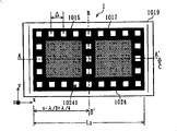
Figure 1A illustrates according to the schematic diagram of first embodiment of the invention from top diffferential capacitor 1 when vertically observing.Figure 1B illustrates the schematic diagram of taking from the cross section of the diffferential capacitor 1 of vertical plane A-A ' when the direction of arrow C is observed among Figure 1A.For the ease of explaining, Figure 1A and 1B also illustrate has three X, the three-dimensional system of coordinate of the vertical axis of Y and Z, wherein the Z axle is corresponding to direction vertically upward, and X, with Y-axis then corresponding to two directions that difference is vertical on horizontal plane.Notice that Y-axis is on the direction identical with arrow C, and extend in the direction of describing after a while parallel with vertical plane B-B '.
In Figure 1A and 1B, diffferential capacitor 1 comprises first capacitor, 1003, the second capacitors 1004, and barricade 1022.In first and second capacitors 1003 and the 1004 shapes interlayer film 1019 on the semiconductor-based end 1020.The semiconductor-based end 1020 and interlayer film 1019 are that what to describe in " background technology " joint in the above with those is identical.First capacitor 1003 and second capacitor 1004 are made up of the wirework of aluminium normally.First capacitor 1003 is included in (that is, this vertical direction) on the Z-direction with therebetween a predetermined space, is in top electrode parallel to each other 1015 and bottom electrode 1016 basically.Top electrode 1015 and bottom electrode 1016 are formed on and leave this vertical plane B-B ' on the position of a preset distance of the negative direction of X-axis.Second capacitor 1014 comprises top electrode 1017 and bottom electrode 1018, and they are with respect to this vertical plane B-B ', and the structure that has respectively top electrode 1015 and bottom electrode 1016 is symmetrical structure basically.
Fig. 2 illustrates the equivalent circuit schematic diagram that is shown in diffferential capacitor 1 among Fig. 1.Fig. 2 is shown in broken lines the cross section of taking from along the diffferential capacitor 1 of vertical plane A-A '.In Fig. 2, first capacitor 1003 and second capacitor 1004 respectively have predetermined capacitor C d.When in-phase signal and inversion signal are supplied to first capacitor 1003 and second capacitor 1004 respectively, or vice versa, produces parasitic capacitance Cpa1 and Cpa2 respectively between barricade 1022 and bottom electrode 1016 and 1018.And, produce parasitic capacitance Cpc and dead resistance Rpc at barricade 1022 with at the semiconductor-based end 1020.In addition, produce parasitic capacitance Cpb 1 and dead resistance Rpb 1 at bottom electrode 1016 with at the semiconductor-based end 1020.Further again, produce parasitic capacitance Cpb2 and dead resistance Rpb2 at bottom electrode 1018 with at the semiconductor-based end 1020.
In conventional diffferential capacitor, lack non-overlapped district An and (see Figure 19 A and 19B, also have Figure 20), thus the parasitic capacitance Cpa1 that takes place between bottom electrode 1016 and the barricade 1021 generally will and the concrete area and the distance dependent between bottom electrode 1016 and barricade 1021 of bottom electrode 1016.This concerning conventional bottom electrode 1018 be right.
On the other hand, adapt with diffferential capacitor 1 according to the present invention and (to see Figure 1A and 1B, also has Fig. 2), with bottom electrode 1016 parasitic capacitance that links being arranged generally is area So according to overlay region Ao, distance D o between overlay region Ao and barricade 1022, the area Sn of non-overlapped district An, and at non-overlapped district An and the distance D n at the semiconductor-based end 1020.This bottom electrode 1018 concerning diffferential capacitor 1 also is right.
Suppose that the area of conventional bottom electrode 1016 (seeing Figure 19 B) equals the area of the bottom electrode 1016 (seeing Figure 1B) according to the present invention, but because distance D n is in fact big than distance D o, so the parasitic capacitance that takes place on the unit are of the bottom electrode 1016 of diffferential capacitor 1 of the present invention is littler than the parasitic capacitance that conventional bottom electrode 1016 takes place.This bottom electrode 1018 concerning diffferential capacitor 1 also is right.
In order to reduce the parasitic capacitance of bottom electrode 1016 unit ares, can reduce the area of overlay region Ao.But, reduce overlay region Ao and can cause parasitic capacitance Cpb1, so the quality factor of first capacitor 1003 are degenerated greatly owing to the influence of dead resistance Rpb 1 greater than parasitic capacitance Cpa1.In other words, between the parasitic capacitance of bottom electrode 1016 unit ares and dead resistance Rpb1, there is coordinated relation.If very the so responsive diffferential capacitor 1 of the influence of dead resistance Rpb1 is applied to differential oscillating circuit 7 (seeing Figure 17), the quality factor of entire circuit will degenerate so.
Fig. 3 is the schematic diagram that a part of structure of the differential oscillating circuit 7 of using diffferential capacitor 1 of the present invention is shown, and this part comprises first and second capacitors 1003 and 1004 and first and second variable capacitors 1005 and 1006.Suppose that first capacitor 1003 has the capacitor C d that mentions in front, and the electric capacity that first variable capacitor 1005 has is Cs.Fig. 3 also illustrates parasitic capacitance Cpa1 and the Cpb1 and the dead resistance Rpb1 of first capacitor 1003 except the dead resistance Rs that first variable capacitor 1005 is shown.
Hereinafter, with reference to figure 3, will be described in rapport above-mentioned from first variable capacitor, 1005 rate of change of capacitance and the viewpoint that is shown in the quality factor of circuit of Fig. 3.In Fig. 3, respectively in-phase signal and inversion signal are supplied to first capacitor 1003 and second capacitor 1004, or vice versa.In addition, 7 pairs of AC signals of differential oscillating circuit (being pointed out by dotted line) have the symmetry with respect to virtual ground.Because the rate of change of capacitance of second variable capacitor 1006 and quality factor are similar to first variable capacitor 1005, so omit to its description.In Fig. 1 and 2, virtual ground corresponding to the crossing a part of barricade 1022 of vertical plane B-B '.
Admittance Y in Fig. 3 between node A and virtual ground is represented by following equation (1):
F is a frequency herein.
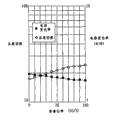
Fig. 4 illustrates to indicate the 1/Y capacitance variations, i.e. the performance diagram of the quality factor of the rate of change of capacitance of first variable capacitor 1005 and first variable capacitor 1005.In Fig. 4, the longitudinal axis on the left side is represented quality factor; The longitudinal axis on the right side is represented rate of change of capacitance; Transverse axis is then represented Duplication.As used herein, rate of change of capacitance is the maximum capacitor value of first variable capacitor 1005 is removed gained by position of minimum capacitance a value, so be that the overlap ratio that the unit with multiple indicates is defined as So/S * 100%, S is the area of bottom electrode 1006 herein, So then is the area of overlay region Ao.The characteristic curve of Fig. 4 is to measure under below the condition: dead resistance Rs is 2 Ω; Dead resistance Rpb1 is 150 Ω; When Duplication was 100%, parasitic capacitance Cpa1 was 0.8pF; And when Duplication was 0%, parasitic capacitance Cpb1 was 0.2pF.Suppose that according to the technical specification of device, first variable capacitor 1005 changes in the scope from 4pF to 2pF.In other words, first variable capacitor 1005 has 2 times rate of change of capacitance.
As shown in Figure 4, when Duplication increased, it is more and more littler than parasitic capacitance Cpa1 that parasitic capacitance Cpb1 becomes, so that the quality factor of entire circuit as shown in Figure 3 are enhanced.The result is that dead resistance Rpb1 is reduced the influence of first variable capacitor 1005, thereby can reduce to minimum to degenerating of entire circuit quality factor as shown in Figure 3.On the contrary, when Duplication descended, the rate of change of capacitance of first variable capacitor 1005 became and approaches " 2 " doubly.Therefore, by with reference to top two Gent linearity curves, in the present embodiment, energy is being chosen in about 70% in quality factor and the rate of change of capacitance optimization Duplication of reducing to minimum that degenerates in the two.But, Duplication can go to select from other viewpoint, rather than as at present embodiment, selects about 70% Duplication with reducing to minimum quality factor and rate of change of capacitance degenerating in the two.For example, the additional more importance that is to degenerate in to quality factor can select Duplication to be equal to or greater than about 70% and less than 100%, on the other hand, for to the degenerating additional more importance in the rate of change of capacitance, can to select Duplication be greater than 0% and be equal to or less than about 70%.
Therefore, the diffferential capacitor 1 according to present embodiment provides barricade 1022, and has selected suitable Duplication again.The result is, can reduce in diffferential capacitor 1 parasitic capacitance and dead resistance and be applied to influence on the differential oscillating circuit 7.In other words, can be in case last degenerating on quality factor on differential oscillating circuit.In addition, can prevent degenerating in the rate of change of capacitance of variable capacitor 1005 and 1006.The result is to prevent the surge frequency range stenosis of differential oscillating circuit 7.
In Fig. 5 A and 5B, the barricade of being made up of electric conducting material 1023 is the parts as plate, and it has the shape of symmetry with respect to vertical plane B-B ', as the situation of barricade 1023.Barricade 1022 is to be inserted between the semiconductor-based end 1020 and two bottom electrodes 1016 and 1018.Barricade 1023 has and is formed on one or more elongated breach 10231.Preferably, elongated breach 10231 (or several cracks mouth) formation is arranged essentially parallel to the x direction of principal axis, and perpendicular to above-mentioned virtual ground.And, for preventing preferably to form elongated breach (or several breach) like this, make the optimization Duplication that limits above be about 70% quality factor and rate of change of capacitance degenerating on the two.Under the occasion that a plurality of elongated breaches 10231 are arranged, form these elongated breaches 10231, along on the direction of x axle, extend parallel to each other.
Though can form these elongated breaches 10231, so that it is parallel on the direction of y axle, but under this occasion, any leakage component (Leak componeut) from differential capacitance 1 will arrive virtual ground place, need long time of cost, and propagate through barricade 1023 in the mode of spiral basically.The result is the induction component to have taken place in barricade 1023, thereby shield effectiveness is degenerated.
In Fig. 6 A and 6B, preferably, barricade 1024 is one with respect to the resembling in the tabular electric conducting material of vertical plane B-B ' symmetry, as the situation of barricade 1022.It is the shape of rectangle basically that barricade 1024 has, and the length of dual-side is Lx respectively, and the direction that is parallel to the x axle is extended.
A plurality of apertures 10241 that run through equal about 70% mode with the optimization Duplication of stipulating above and are formed in the barricade 1024, so that prevent degenerating on quality factor and rate of change of capacitance.For clarity, an aperture that only runs through in Fig. 6 A and 6B in the aperture is flagged as " 10241 ".Preferably, run through aperture 10241 be configured be arranged essentially parallel to x direction of principal axis and y direction of principal axis the two.Under this occasion, just have odd number run through the aperture alignment be configured be parallel to y direction of principal axis (being referred to as " row " hereinafter) (shown in Fig. 6 A and the 6B this classify as 9 row).Any two apertures 10241 that run through that adjoin along the x direction of principal axis are placed in from they distance, delta places at center separately.
In-phase signal and inversion signal also leak into barricade 1024 from diffferential capacitor 1.A kind of like this wavelength that leaks component is relevant with the frequency of homophase and inversion signal, so be known.Suppose that this wavelength that leaks component is λ, the nearly regulation of distance that extends to virtual ground (vertical plane B-B ') from each dual-side of the barricade 1024 that is parallel to the y axle should be
 In other words, Lx=λ (n+1/2), n refers to columns (n is equal to or greater than zero integer) herein.
As shown in Figure 7, having wavelength is that the standing wave of λ will be propagated on barricade 1024.This standing wave has the center is fixed on the node every λ/2 around the virtual ground.Because standing wave is little at the amplitude of each node, so preferably be formed on the position corresponding to node i.e. Δ=λ/2 running through aperture 10241.Therefore can prevent of the leakage of this standing wave from each through hole 10241 to the semiconductor-based end 1020.The result is to prevent degenerating on diffferential capacitor 1 quality factor.
Though resemble latticelike array at the aperture 10241 that runs through shown in Fig. 6 A and the 6B, other configuration also is possible.For example, can be configured in perforation aperture 10241 coaxial circles of some centering on every side in the virtual ground, the distance between per two coaxial circles that adjoin is a Δ.
In diffferential capacitor 1, can be barricade 1022,1023 or 1024 by inductor or resistance-grounded system (not shown), to prevent the electric charge accumulation.Perhaps can the virtual ground in barricade 1022,1023 or 1024 directly electrical ground (not shown) to prevent the electric charge accumulation in barricade 1022,1023 or 1024.
(second embodiment)
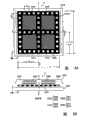
Fig. 8 A illustrates according to second embodiment of the invention, from the schematic diagram of top diffferential capacitor 2 when vertically observing.Fig. 8 B illustrates to take from that vertical plane A-A ' locates among Fig. 8 A, the cross sectional representation of the diffferential capacitor 2 when the direction of arrow C is observed.For the ease of explaining, Fig. 8 A and 8B also illustrate has three X, the three-dimensional system of coordinate of the vertical axis of Y and Z, and wherein the Z axle is corresponding to direction vertically upward, and X and Y-axis then correspond respectively to the vertical direction on the horizontal plane.Note Y-axis be with the equidirectional of arrow C on, and be parallel to the vertical plane B-B ' that describes after a while.
In Fig. 8 A and 8B, diffferential capacitor 2 comprises first to the 4th capacitor 2001 to 2004 and the barricade 2005.First to the 4th capacitor 2001 to 2004 is formed in the interlayer film 1019 at the semiconductor-based end 1020.The semiconductor-based end 1020 and interlayer film 1019 are described in " background technology " joint to be identical in the above with those.First to the 4th capacitor 2001 to 2004 normally is made up of the wirework of aluminium.First capacitor 2001 comprises top electrode 2006 and bottom electrode 2007, and they are along Z-direction (vertically), disposes with a predetermined interval with being substantially parallel to each other.Top electrode 2006 and bottom electrode 2007 are formed on the positive direction towards Y-axis, leave predetermined distance of vertical plane A-A ' (it is parallel to X-direction and extends), and, leave on the position of a preset distance of vertical plane B-B ' (it is parallel to Y direction and extends) in direction towards X-axis.
Barricade is the sheet as plate of electric conducting material preferably, and it is symmetrical with respect to vertical plane A-A ' with respect to vertical plane B-B '.More precisely, barricade 2005 has the foursquare basically shape that every limit length of side is L.Barricade 2005 is configured in is positioned between the semiconductor-based end 1020 and all bottom electrode 2007,2009,2011 and 2013.
A plurality of apertures 20051 that run through are formed in the barricade 2005.For clarity, in Fig. 8 A and 8B, only marked an aperture that runs through in the aperture and be " 20051 ", run through aperture 2005 and be configured in X-direction and Y direction.The aperture 20051 that runs through of odd several alignments is parallel to the Y-axis extension, and the aperture 20051 that runs through of odd several alignments is parallel to X-axis extension (such array has 9 in Fig. 8 A and 8B).Hereinafter, the aperture alignment that runs through that is parallel to the Y-axis extension is referred to as " row ", and the aperture alignment that runs through that is parallel to the X-axis extension then is referred to as " OK ".Running through aperture 2005 disposes in such a way, the center of respectively running through aperture 20051 of promptly forming middle column is being on the crossing single line of barricade 2005 and vertical plane B-B ', and the center of respectively running through aperture 20051 of row is on the crossing single line of barricade 2005 and vertical plane B-B ' in the middle of forming, and the center of respectively running through aperture 20051 of row then is on the crossing single line of barricade 2005 and vertical plane A-A ' in the middle of forming.Ask along X-axis side or any two apertures 20051 that run through that adjoin of Y direction to be configured in from the distance between they centers separately be the place of Δ.
In diffferential capacitor 2 with said structure, form the differential right coaxial signal of signal and supply to first capacitor 2001 and the 4th capacitor 2004, they are formed on respect at vertical plane A-A ', vertical plane B-B ', and on the point-symmetric each other position of the intersection point between the barricade 2005.Form the differential right inversion signal of signal and supply to second capacitor 2002 and the 3rd capacitor 2003, they are formed on respect on the point-symmetric each other position of intersection point above-mentioned.By in-phase signal and inversion signal are provided in this way, become the parasitic capacitance that might reduce in diffferential capacitor 2 and dead resistance and be applied to influence on the differential oscillating circuit 7 as in first embodiment.
With the same reason described in first embodiment, distance from each two side of being parallel to the barricade 2005 that Y-axis extends to virtual ground (vertical plane B-B ') and the distance from each two side of the descending barricade 2005 that extends in X-axis to virtual ground (vertical plane A-A ') are respectively to be defined as n λ/2+ λ/4, and n refers to the number (n is equal to or greater than zero integer) of row and column herein.With the same reason of describing at first embodiment, it preferably
Though top description has illustrated diffferential capacitor and has comprised that two capacitors (along X-direction) take advantage of two capacitors (along Y direction) that the present invention is not limited to this.In other words, (capacitor is represented by the hacures that descend to the right herein) according to above-mentioned principle as shown in Figure 9, and diffferential capacitor 2 can comprise that three or more capacitor (along X-direction) takes advantage of three or more capacitor (along Y direction).Under this occasion, preferably, equaling n λ along the distance between X-axis or any two virtual grounds of adjoining of Y-axis.
(the 3rd embodiment)
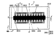
Figure 10 A is according to third embodiment of the invention, from the schematic diagram of top diffferential capacitor 3 when vertically observing.Figure 10 B illustrates to take from vertical plane A-A ' among Figure 10 A, the cross-sectional view of the diffferential capacitor 3 when the direction of arrow C is observed, for example in explanation, Figure 10 A and 10B also illustrate has X, the three-dimensional system of coordinate of three vertical axises of Y and Z, wherein the Z axle is corresponding to direction vertically upward, X and Y then corresponding on horizontal plane two directions that difference is vertical.Notice that Y-axis is identical with the direction of arrow C, and be parallel to the vertical plane B-B ' extension of describing after a while.
In Figure 10 A and 10B, diffferential capacitor 3 comprises first to the 4th capacitor 3001 to 304 and the barricade 3005.First to the 4th capacitor 3001 to 3004 is formed on and produces in the conductor substrate 1020 in the interlayer film 1019.Described in " background technology " saves in the above with those with interlayer film 1019 at the semiconductor-based end 1020 is identical.
First to the 4th capacitor 3001 to 3004 normally is made up of the aluminum metal squeeze.
Similarly, second electric capacity 3002 comprises first motor and 3015 and second electrode 3016.Second electric capacity 3002 is formed on the negative direction towards X-axis, from being on the position of position upper and lower translation one preset distance of substantial symmetry from first electrode 3015 with respect to vertical plane A-A '.The result is, and is the same with first capacitor 3001, producing edge capacitance between the broach along adjoining of X-direction.In addition, also can produce edge capacitance at first capacitor 3001 and second capacitor 3002 along adjoining between the comb teeth part branch of Z-direction.
It is on the position of substantial symmetry that the 3rd capacitor 3003 is formed on from first capacitor 3001 with respect to vertical plane B-B '.It is on the position of substantial symmetry that the 4th capacitor 3004 is formed on from second capacitor 3002 with respect to vertical plane B-B '.Therefore, as mentioned above, in third and fourth capacitor 3003 and 3004, also can produce edge capacitance.
Figure 11 illustrates the equivalent circuit schematic diagram that is shown in Figure 10 A and 10B diffferential capacitor 3.In Figure 11,, suppose that broach part A1 is the broach part on the left side of second electrode 3016 of first capacitor 3001 as an example.Under this hypothesis, broach part A2 is the broach part that is positioned in abutting connection with second electrode 3016 of first capacitor 3001 of broach part A1, broach part B1 is the broach part on the left side of first electrode 3015 of first capacitor 3001, and broach part B2 is the broach part that is positioned in abutting connection with first electrode 3015 of first capacitor 3001 of broach part B1.
Broach part B3 is along the z direction of principal axis, in the broach part of second capacitor 3002 on broach part A1 opposite.Broach part B4 along the z direction of principal axis, in the broach part of second capacitor 3002 on broach part A2 opposite.
Broach part A3 is along the z direction of principal axis, in the broach part of second capacitor 3002 on broach part B1 opposite.Broach part A4 is along the z direction of principal axis, in the broach part of second capacitor 3002 on broach part B2 opposite.
When the differential right in-phase signal of signal and inversion signal are supplied with first and second capacitors 3001 with said structure and 3002, broach part A1 will have edge capacitance C11 between the side of itself and broach part B1.Broach part A1 and B3 below broach part A1 face and the face above the broach part B3 between capacitor C 13 will be arranged.Equally, with respect to other broach part, edge capacitance C21, C22, C33, C34 and C44 also will produce, and as shown in figure 11, also have capacitor C 31, and C14 and C42 will produce.So, at broach part A1 to A4 and B1 to the total capacitance C that takes place between the B4
AlwaysCan express by following equation (2):
C
Always=C11+C13+C33+C31+C22+C21+C24+C34+C22+C42+C44 (2)
Barricade 3005 is by the parts of forming such as the electric conducting material of aluminium as plate, and its along continuous straight runs has the shape of symmetry with respect to vertical plane B-B '.Barricade 3005 is inserted in the semiconductor-based end 1020 and second capacitor 3002 and the 4th capacitor 3004 between the two, barricade 3005 has such shape, make when second capacitor 3002 and the 4th capacitor 3004 from top when vertically projecting to barricade 3005, is thrown second capacitor 3002 of lining and the 4th capacitor 3004 look like and barricade 3005 partly overlapping.As the previous embodiment, overlapping each of the image of its projection and barricade 3005 and the part of second capacitor 3002 and the 4th capacitor 3004 will be referred to as " overlay region Ao ".
Diffferential capacitor 3 with top structure, by the barricade 3005 that below the second and the 4th capacitor 3002 and 3004, provides, produced parasitic capacitance Cpa and Cpd (the with dashed lines figure illustrates) as shown in figure 12 between the face below the face on barricade 3005 and broach part A3, A4, B3 and the B4.Differential when diffferential capacitor 3 is incorporated into, during oscillating circuit 7, for example, these parasitic capacitances Cpa and Cpd will influence the scope of its frequency of oscillation.On the other hand, if omit screen 3005, owing to resemble the same reason described in first embodiment, the diffferential capacitor 3 as the semiconductor-based end 1020, are coupled by the big parasitic capacitance that two sides at diffferential capacitor 3 produce, and make the dead resistance influence that produces in the semiconductor-based end 1020 become remarkable.The result is that the quality factor of diffferential capacitor 3 can degenerate, thereby influence the C/N (charge carrier is to the ratio of noise) of differential oscillating circuit.But, Duplication in the present embodiment also can resemble described in the embodiment in front optimised, thereby degenerating in the surge frequency range of differential oscillating circuit 7 reduced to minimum, also C/N in differential oscillating circuit 7 is degenerated and reduces to minimum.In the present embodiment, Duplication is defined as (SO/S) * 100[%], S is second capacitor 3002 and the 4th capacitor 3004 face and the gross area below herein, and So then is the gross area of overlay region Ao in second capacitor 3002 and the 4th capacitor 3004.
Figure 13 is the structural representation that illustrates according to fourth embodiment of the invention differential switch circuit 4.In Figure 13, differential switch circuit 4 comprises: differential input terminal 4001, is used to receive the input 4002 of control signal; P ditch MOSFET (metal → oxide → semiconductor field effect transistor) 4003, two n ditch MOSFET4004 and 4005, any in the diffferential capacitor described in the embodiment 1 to 3 in front; And differential output end 4006.
Being used to change MOSFET4003 to 4005 makes its dual signal of opening or turn-offing (being referred to as hereinafter, " control signal ") Vct1 be input to input 4002.
MOSFET4003 is connected to input 4002, and when control signal Vct1 when high level (Hi) by open-minded.On the other hand, when control signal Vct1 when low level (Lo), MOSFET4003 is turned off.
MOSFET4004 and 4005 is connected to input 4002, and is turned off when control signal Vct1 is " Hi ".On the other hand, when control signal Vct1 was " Lo ", MOSFET4004 and 4005 was by open-minded.
In the differential switch circuit 4 of structure, in-phase signal and inversion signal are input to terminal IN respectively on have
+And IN
-Control signal with " Hi " or " Lo " value is input to input 4002.
When control signal Vct1 was " Hi ", n ditch MOSFET4004 and 4005 was opened and p ditch MOSFET4003 is turned off, so in-phase signal and inversion signal are respectively from terminal OUT
+And OUT
-Output.
On the other hand, when control signal Vct1 is " Lo ", n ditch MOSFET4004 and 4005 be turned off and p ditch MOSFET4003 by open-minded, so terminal OUT
+And OUT
-Basically isolate fully with differential switch circuit 4.The result is terminal OUT
+And OUT
-Do not export in-phase signal and inversion signal.
In diffferential capacitor 1,2 or 3, should limit according to the quality factor of the isolation when MOSFET4003 circuit (playing a part switch) turn-offs and each electric capacity at the folded area of the weight between the bottom electrode that respectively is projected and each barricade.
As control signal Vct
1When being " Hi ", bias voltage is added in the leakage and source of MOSFET4003.But, can cut off the DC component of n- channel mosfet 4004 and 4005 by diffferential capacitor 1,2 or 3.
For the technical result that provides by present embodiment is provided, the problem that may cause will be described in conventional diffferential capacitor rather than the diffferential capacitor 1 to 3 under any situation about being incorporated in the switching circuit.If lacking the diffferential capacitor of barricade is incorporated in the switching circuit, then when switching circuit is opened, because the influence on the dead resistance road that in the semiconductor-based end, takes place, so the insertion loss that is caused by the insertion of switching circuit increases, therefore, cause differential the reducing of signal exported to intensity.Be incorporated under the situation that its Duplication that is defined as above is 100% diffferential capacitor, the parasitic capacitance that takes place between each capacitor and barricade will make the unlikely quilt of p ditch MOSFET4003 turn-off fully, make that the signal that is input to differential input terminal 4001 is differential to leaking by parasitic capacitance.The result is, when n channel mosfet 4004 and 4005 when opening, switching circuit will have the insertion loss of increase, make the differential right intensity of output signal degenerate.On the contrary, if use in the above-described diffferential capacitor 1 to 3 any, parasitic capacitance is reduced to minimum, so can realize having the switching circuit 4 of little insertion loss.
(the 5th embodiment)
Figure 14 A illustrates according to fifth embodiment of the invention, at the schematic diagram from top differential antenna element 5 when vertically observing.Figure 14 B takes from that vertical plane A-A ' locates among Figure 14 A, the cross sectional representation of the diffferential capacitor 5 when the direction of arrow C is observed.Explain that for convenience Figure 14 A and 14B illustrate has X, the three-dimensional system of coordinate of three vertical axises of Y and Z, wherein the Z axle is corresponding to direction vertically upward, and X and Y-axis then correspond respectively to the vertical direction on horizontal plane.Note Y-axis be with the equidirectional of arrow C on, and be parallel to the vertical plane B-B ' that describes after a while and extend.
In Figure 14 A and 14B, differential antenna element 5 comprises: first planar antenna element, 5001, the second planar antenna element 5002 and barricade 5003.
First and second planar antenna element 5001 and 5003 are formed in the interlayer film 1019 at the semiconductor-based end 1020.The semiconductor-based end 1020 and interlayer film 1019 are identical with those descriptions in " background technology " joint.First and second planar antenna element are made up of the sheet as plate of dielectric substance usually.
First planar antenna element 5001 is vertically to make progress in the positive direction towards the Z axle, and 1,020 one predetermined distances are configured from the semiconductor-based ends, and is formed on negative direction towards X-axis on the position of a vertical plane B-B ' preset distance.
Second planar antenna element 5002 has the shape substantially the same with first plane component 5001, and is formed on the place from first planar antenna element, 5001 substantial symmetry with respect to vertical plane B-B '.
In lacking the differential antenna element of barricade, the gain of differential antenna element is had the loss that links to reduce with the dead resistance that takes place in the semiconductor-based end.And, in conventional differential antenna element, in the frequency bandwidth of the capable transmission of each planar antenna element, because the parasitic capacitance that takes place between barricade and planar antenna element is by stenosis.On the contrary, by using present embodiment barricade 5003, its Duplication is optimised as described in the embodiment in front, just might reduce to minimum to degenerating in the frequency bandwidth of the transmission of having the ability in first and second planar antenna element 5001 and 5002, and prevent reduction in first and second planar antenna element 5001 and 5002 gains.
Have and the same structure that is shown among Fig. 6 A and the 6B though present embodiment illustrates barricade 5003, the present invention is to being not limited thereto.It will be appreciated that the barricade described in arbitrary embodiment in front, or its equivalence can be used as all and substitutes and be used.
(the 6th embodiment)
Figure 15 is the total circuit construction schematic diagram that illustrates according to sixth embodiment of the invention filter circuit 6.In Figure 15, filter circuit 6 comprises 601, two half-wave resonator 602a of differential input terminal and 602b, two capacitor 603a and 603b, and differential end 604.
Differential input terminal 601 comprises being respectively applied for to receive forms the differential right in-phase signal of signal and the terminal IN of inversion signal
+With terminal IN
-
Two half- wave resonator 602a and 602b are with respect to terminal IN
+With terminal IN
-Be connected in parallel.Figure 16 A illustrate from top when vertically observing half-wave resonator 602a among Figure 15 and the schematic diagram of 602b.Figure 16 B illustrates and takes from that vertical plane A-A ' locates in Figure 16 A, half-wave resonator 602a when the direction of arrow C is observed and the cross sectional representation of 602b.Explain that for convenience Figure 16 a and 16b also illustrate has X, the three-dimensional system of coordinate of Y and three vertical axises of Z, wherein the Z axle is corresponding to direction vertically upward, and X and Y-axis then correspond respectively to the vertical direction on horizontal plane.Note Y-axis be the branch arrow C on identical direction, extend and be parallel to the vertical plane B-B ' that describes after a while.Because half-wave resonator 602a has identical structure with 602b, so only describe half-wave resonator 602a below.
In Figure 16 A and 16B, half-wave resonator 602a comprises surface plate 6021 and the barricade 6022 as band.Surface plate 6021 is formed in the suprabasil interlayer film 1019 of semiconductor.The semiconductor-based end 1020 and interlayer film 1019 described in " background technology " joint is identical with those.By having positive direction (vertically) that surface plate 6021 that the dielectric resistance material forms is formed in the Z axle on the position of a preset distance at the semiconductor-based end 1020, and have on the position with respect to vertical plane B-B ' symmetry.Surface plate 6021 has first terminal 6023 and second terminal 6024, and they are formed at each other on the position with respect to vertical plane B-B ' symmetry.First terminal 6023 and second terminal 6024 of surface plate 6021 are connected respectively to terminal IN
+With terminal IN
-
Capacitor 603a is connected between node N1 and the node N2, and wherein node N1 is terminal IN
+Be connected to the point of half-wave resonator 602a, node N2 then is terminal OUT
+Be connected to the point of half-wave resonator 602b.
Capacitor 603b is connected between node N3 and the node N4, and wherein node N3 is terminal IN
-Be connected to the point of half long resonator 602a, node N4 then is terminal OUT
-Be connected to the point of half-wave resonator 602b.
Return with reference to Figure 15, differential output end 604 comprises being respectively applied for forms the differential right in-phase signal of signal and the terminal OUT of inversion signal
+With terminal OUT
-
On have in the filter circuit 6 of structure, when signal with required frequency when being input to differential input terminal 601, the impedance of half- wave resonator 602a and 602b is very high, as the result of this thing is, signal is to from differential output end 604 outputs.
On the other hand, if signal with the frequency that is different from required frequency to being input to differential input terminal 601, then the impedance of half- wave resonator 602a and 602b becomes very little, as the result of this thing, then is that the output at differential output end 604 places is suppressed.
If the half-wave resonator that lacks barricade is applied to filter circuit,, and the insertion loss of filter circuit is increased then owing to the loss that links is arranged with the dead resistance that takes place at the semiconductor-based end.In its Duplication as surface defined is that 100% half-wave resonator is applied under the occasion of filter circuit, and the parasitic capacitance that takes place between barricade and surface plate will reduce the transmission frequency of filter circuit.On the contrary, by using barricade 6022 according to present embodiment, its Duplication resemble described in the embodiment in front optimised, just might reduce to minimum to the insertion loss of filter circuit 6, and prevent degenerating of its transmission frequency bandwidth.
Have the exemplary example that resembles at the same structure shown in Fig. 6 A and the 6B though present embodiment shows barricade 6022, the present invention is not limited to this.Will appreciate that the barricade described in the embodiment of arbitrary front, or its equivalence all can be used as substitute and uses.
Although the present invention has done the description of details, the description of front all is exemplary rather than restrictive in all respects.Know in the case without departing from the scope of the present invention, can create numerous other modification and variation.
Claims (33)
1, a kind of diffferential capacitor (1,2,3) that comprises a plurality of capacitors (1003 and 1004,2002-2004 or 3001-3004), each capacitor all has top electrode vertically parallel to each other and bottom electrode, it is characterized in that:
First capacitor in described a plurality of capacitor is formed on the position with respect to the second capacitor symmetry in vertical plane and the described a plurality of capacitor at semiconductor-based the end,
Diffferential capacitor also comprises and is inserted in each bottom electrode and the barricade at the described semiconductor-based end (1022-1024,1005 or 3005),
Described barricade passes through inductor and/or resistance-grounded system,
When each bottom electrode vertically was projected on the barricade, bottom electrode that respectively is projected and described barricade have overlapped, and
The overlapping of bottom electrode that respectively is projected and barricade account for altogether the bottom electrode area 70% or more.
2, diffferential capacitor according to claim 1 is characterized in that, the bottom electrode that respectively is projected extends in the outside of barricade.
3, diffferential capacitor according to claim 1 is characterized in that, barricade has the elongated breach that is formed on wherein.
4, diffferential capacitor according to claim 3 is characterized in that, this elongated breach and this vertical plane intersect.
5, diffferential capacitor according to claim 1 is characterized in that, this barricade has a plurality of apertures that run through that are formed on wherein.
6, diffferential capacitor according to claim 5 is characterized in that,
These a plurality of apertures that run through dispose along two predetermined directions with the interval that equates, and
A plurality of spacings that run through between the aperture that aperture adjoins equal 1/2 wavelength that an integer multiply by the standing wave of propagating through barricade.
7, diffferential capacitor according to claim 6 is characterized in that, equals the integral multiple and the 1/4 described standing wave wavelength sum of described standing wave 1/2 wavelength to the length of this vertical plane from two predetermined sides of barricade.
8, diffferential capacitor according to claim 1 is characterized in that, between a plurality of capacitors, any two capacitors that adjoin each other receive respectively forms differential right in-phase signal of signal and inversion signal.
9, diffferential capacitor according to claim 1 is characterized in that, the part that described barricade and this vertical plane intersect is a ground connection.
10, diffferential capacitor according to claim 1 is characterized in that, described diffferential capacitor is used for variable capacitance circuit, and wherein at least one variable capacitor is connected to each bottom electrode or at least one variable capacitor is connected to each top electrode.
11, diffferential capacitor according to claim 10 is characterized in that, the partly overlapping area of bottom electrode that respectively is projected and barricade decides according to the rate of change of capacitance of variable capacitance circuit and the quality factor of each capacitor.
12, diffferential capacitor according to claim 1 is characterized in that, described diffferential capacitor is used for differential oscillating circuit.
13, diffferential capacitor according to claim 1 is characterized in that, described diffferential capacitor is used for variable capacitance circuit, wherein at least one switch element is connected to the bottom electrode of described first capacitor and the bottom electrode of described second capacitor.
14, diffferential capacitor according to claim 13 is characterized in that, the partly overlapping area of bottom electrode that wherein respectively is projected and barricade decides according to the quality factor of the isolation when this switching circuit is turned off and each capacitor.
15, diffferential capacitor according to claim 1 is characterized in that, described diffferential capacitor is used for the differential switch circuit.
16, diffferential capacitor according to claim 1 is characterized in that,
In a plurality of capacitors first to be being formed on from the position with respect to any one the capacitor symmetry in a plurality of capacitors of this vertical plane at semiconductor-based the end,
In a plurality of capacitors second being formed on from described any one the symmetrical position with respect to the described a plurality of capacitors that are positioned at another vertical plane vertical with this vertical plane at semiconductor-based the end, and
The 3rd of a plurality of capacitors to be formed on from described any one the symmetrical position with respect to described a plurality of capacitors of the intersecting lens between this vertical plane and this another vertical plane at semiconductor-based the end.
17, diffferential capacitor according to claim 16, it is characterized in that, form differential right in-phase signal of signal and inversion signal and offer a plurality of capacitors by this way, promptly provide described any one and the 3rd capacitor that is given to described a plurality of capacitors one in in-phase signal or the inversion signal, and in in-phase signal or the inversion signal another offered first and second capacitor of described a plurality of capacitors.
18, diffferential capacitor according to claim 16 is characterized in that,
This barricade has a plurality of apertures that run through that are formed on wherein, these run through aperture and dispose along two predetermined directions with the interval that equates, make a plurality of spacings that run through between the aperture that aperture adjoins equal the integral multiple of 1/2 wavelength of the standing wave propagated through this barricade, and
This barricade has the shape of rectangle, make from two predetermined sides of barricade to this vertical plane length and all equal the integral multiple and the 1/4 described standing wave wavelength sum of described standing wave 1/2 wavelength to the length of this another vertical plane from other dual-side of barricade.
19, a kind of differential antenna element is characterized in that, this antenna element comprises:
A plurality of antenna elements, they are formed on the position that is mutually symmetrical with respect to vertical plane at semiconductor-based the end, and
Barricade is inserted in each antenna element and at described the semiconductor-based end,
Described barricade passes through inductor and/or resistance-grounded system,
Wherein, when each antenna element vertically was projected on this barricade, the antenna element that respectively is projected and this barricade overlapped, and
The overlapping of antenna element that respectively is projected and barricade account for altogether described antenna element area 70% or more.
20, differential antenna element according to claim 19 is characterized in that, the antenna element that respectively is projected extends in this barricade outside.
21, differential antenna element according to claim 19 is characterized in that, this barricade has the elongated breach that is formed on wherein.
22, differential antenna element according to claim 21 is characterized in that, this elongated breach and this vertical plane intersect.
23, differential antenna element according to claim 19 is characterized in that, this barricade has a plurality of apertures that run through that are formed on wherein.
24, differential antenna element according to claim 19 is characterized in that, between a plurality of antenna elements, any two antenna elements that adjoin each other receive respectively forms differential right in-phase signal of signal and inversion signal.
25, differential antenna element according to claim 19 is characterized in that, the part that described barricade and this vertical plane intersect is a ground connection.
26, a kind of suprabasil differential resonator of semiconductor (602a or 602b) that is formed on is characterized in that described resonator comprises:
At least one dielectric surface plate (6021) has the shape with respect to the symmetry of vertical plane, and has two terminals (6023,6024) that are mutually symmetrical with respect to described vertical plane, and
Barricade (6022) is configured at least one surface plate and at described the semiconductor-based end,
Barricade passes through inductor and/or resistance-grounded system,
Wherein, when described at least one surface plate when the plane vertical direction is projected to this barricade, described at least one surface plate that is projected and this barricade overlap, and
The overlapping of described at least one surface plate that is projected and barricade account for altogether described at least one surface plate area that is projected 70% or more.
27, differential resonator according to claim 26 is characterized in that, at least one surface plate that is projected extends in this barricade outside.
28, differential resonator according to claim 26 is characterized in that, this barricade has the elongated breach that is formed on wherein.
29, differential resonator according to claim 28 is characterized in that, this elongated breach and this vertical plane intersect.
30, differential resonator according to claim 26 is characterized in that, this barricade has a plurality of apertures that run through that are formed on wherein.
31, differential resonator according to claim 26 is characterized in that, described two terminals of described at least one surface plate receive respectively forms right in-phase signal and the inversion signal of differential wave.
32, differential resonator according to claim 26 is characterized in that, the part that described barricade and this vertical plane intersect is a ground connection.
33, differential resonator according to claim 26 is characterized in that, described differential resonator is used for filter circuit.
Applications Claiming Priority (3)
| Application Number | Priority Date | Filing Date | Title |
|---|---|---|---|
| JP2003-191267 | 2003-07-03 | ||
| JP2003191267 | 2003-07-03 | ||
| JP2003191267 | 2003-07-03 |
Publications (2)
| Publication Number | Publication Date |
|---|---|
| CN1577857A CN1577857A (en) | 2005-02-09 |
| CN100426505C true CN100426505C (en) | 2008-10-15 |
Family
ID=33447963
Family Applications (1)
| Application Number | Title | Priority Date | Filing Date |
|---|---|---|---|
| CNB200410062884XA Expired - Fee Related CN100426505C (en) | 2003-07-03 | 2004-07-05 | Differential capacitor, differential antenna element, and differential resonator |
Country Status (3)
| Country | Link |
|---|---|
| US (1) | US6940707B2 (en) |
| EP (1) | EP1496528B1 (en) |
| CN (1) | CN100426505C (en) |
Families Citing this family (11)
| Publication number | Priority date | Publication date | Assignee | Title |
|---|---|---|---|---|
| US8238075B2 (en) * | 2006-02-22 | 2012-08-07 | Vishay Sprague, Inc. | High voltage capacitors |
| US7336475B2 (en) * | 2006-02-22 | 2008-02-26 | Vishay Vitramon, Inc. | High voltage capacitors |
| WO2009108756A1 (en) * | 2008-02-26 | 2009-09-03 | Softspikes, Llc | Improved traction cleat for field sports |
| WO2011033659A1 (en) * | 2009-09-18 | 2011-03-24 | 株式会社 東芝 | Wireless device |
| US9054069B2 (en) * | 2013-09-05 | 2015-06-09 | International Business Machines Corporation | Variable capacitance integrated circuit |
| TWI500934B (en) * | 2013-09-11 | 2015-09-21 | Pixart Imaging Inc | Micro-electro-mechanical device having differential capacitors of corresponding sizes |
| US9739816B2 (en) * | 2013-11-27 | 2017-08-22 | Analog Devices, Inc. | Capacitive sensor with differential shield |
| CN105338399A (en) * | 2015-10-29 | 2016-02-17 | 小米科技有限责任公司 | Image acquisition method and device |
| US10224363B2 (en) | 2016-07-28 | 2019-03-05 | Neteera Technologies Ltd. | Terahertz CMOS sensor |
| CN110323334B (en) * | 2019-07-09 | 2023-03-24 | 四川中微芯成科技有限公司 | Structure and method for using parasitic capacitor as ADC capacitor |
| CN116632001B (en) * | 2023-07-24 | 2023-10-13 | 合肥晶合集成电路股份有限公司 | Semiconductor device and design assisting device for semiconductor device |
Citations (5)
| Publication number | Priority date | Publication date | Assignee | Title |
|---|---|---|---|---|
| JPH06177325A (en) * | 1992-12-10 | 1994-06-24 | Fujitsu Ltd | Semiconductor capacitance element and circuit using the same |
| US6348722B1 (en) * | 1999-08-24 | 2002-02-19 | Nec Corporation | Semiconductor memory with shield layer |
| US6366433B1 (en) * | 1999-02-24 | 2002-04-02 | Mitsumi Electric Co., Ltd. | Large-capacity magnetic disk drive having head load pressure adjustment |
| US6456481B1 (en) * | 2001-05-31 | 2002-09-24 | Greatbatch-Sierra, Inc. | Integrated EMI filter-DC blocking capacitor |
| US20020171115A1 (en) * | 2001-05-17 | 2002-11-21 | Matsushita Electric Industrial Co., Ltd. | High frequency semiconductor device |
Family Cites Families (16)
| Publication number | Priority date | Publication date | Assignee | Title |
|---|---|---|---|---|
| US171115A (en) * | 1875-12-14 | Improvement in millstones | ||
| US201846A (en) * | 1878-03-26 | Improvement in beer-pumps | ||
| US5220483A (en) | 1992-01-16 | 1993-06-15 | Crystal Semiconductor | Tri-level capacitor structure in switched-capacitor filter |
| US5760456A (en) * | 1995-12-21 | 1998-06-02 | Grzegorek; Andrew Z. | Integrated circuit compatible planar inductors with increased Q |
| JP2000500240A (en) * | 1996-08-29 | 2000-01-11 | フィリップス エレクトロニクス ネムローゼ フェンノートシャップ | Frequency-independent voltage divider |
| US6366443B1 (en) * | 1997-12-09 | 2002-04-02 | Daniel Devoe | Ceramic chip capacitor of conventional volume and external form having increased capacitance from use of closely-spaced interior conductive planes reliably connecting to positionally-tolerant exterior pads through multiple redundant vias |
| US6066537A (en) * | 1998-02-02 | 2000-05-23 | Tritech Microelectronics, Ltd. | Method for fabricating a shielded multilevel integrated circuit capacitor |
| US6097195A (en) * | 1998-06-02 | 2000-08-01 | Lucent Technologies Inc. | Methods and apparatus for increasing metal density in an integrated circuit while also reducing parasitic capacitance |
| US6489663B2 (en) * | 2001-01-02 | 2002-12-03 | International Business Machines Corporation | Spiral inductor semiconducting device with grounding strips and conducting vias |
| JP4047064B2 (en) | 2001-05-17 | 2008-02-13 | 松下電器産業株式会社 | High frequency semiconductor device |
| JP3977053B2 (en) * | 2001-10-30 | 2007-09-19 | 富士通株式会社 | Capacitor element and manufacturing method thereof |
| JP3842111B2 (en) * | 2001-11-13 | 2006-11-08 | 富士通株式会社 | Semiconductor device and manufacturing method thereof |
| JP2003188338A (en) * | 2001-12-13 | 2003-07-04 | Sony Corp | Circuit board and its manufacturing method |
| JP3748556B2 (en) | 2002-03-15 | 2006-02-22 | 松下電器産業株式会社 | Balanced high-frequency device |
| EP1345323B1 (en) | 2002-03-15 | 2005-02-09 | Matsushita Electric Industrial Co., Ltd. | Balanced high-frequency device and balance-characteristics improving method and balanced high-frequency circuit using the same |
| JP4933036B2 (en) * | 2003-07-03 | 2012-05-16 | パナソニック株式会社 | Differential capacitance element, differential antenna element, and differential resonance element |
-
2004
- 2004-07-01 EP EP04015456A patent/EP1496528B1/en not_active Not-in-force
- 2004-07-01 US US10/880,531 patent/US6940707B2/en active Active - Reinstated
- 2004-07-05 CN CNB200410062884XA patent/CN100426505C/en not_active Expired - Fee Related
Patent Citations (5)
| Publication number | Priority date | Publication date | Assignee | Title |
|---|---|---|---|---|
| JPH06177325A (en) * | 1992-12-10 | 1994-06-24 | Fujitsu Ltd | Semiconductor capacitance element and circuit using the same |
| US6366433B1 (en) * | 1999-02-24 | 2002-04-02 | Mitsumi Electric Co., Ltd. | Large-capacity magnetic disk drive having head load pressure adjustment |
| US6348722B1 (en) * | 1999-08-24 | 2002-02-19 | Nec Corporation | Semiconductor memory with shield layer |
| US20020171115A1 (en) * | 2001-05-17 | 2002-11-21 | Matsushita Electric Industrial Co., Ltd. | High frequency semiconductor device |
| US6456481B1 (en) * | 2001-05-31 | 2002-09-24 | Greatbatch-Sierra, Inc. | Integrated EMI filter-DC blocking capacitor |
Also Published As
| Publication number | Publication date |
|---|---|
| US6940707B2 (en) | 2005-09-06 |
| CN1577857A (en) | 2005-02-09 |
| EP1496528A3 (en) | 2009-07-22 |
| US20050002149A1 (en) | 2005-01-06 |
| EP1496528A2 (en) | 2005-01-12 |
| EP1496528B1 (en) | 2012-09-05 |
Similar Documents
| Publication | Publication Date | Title |
|---|---|---|
| CN100426505C (en) | Differential capacitor, differential antenna element, and differential resonator | |
| CN1921035B (en) | Cross-coupled inductor pair formed in an integrated circuit | |
| US5898403A (en) | Antenna formed of multiple dielectric substrates including shielded LC filter | |
| US5640134A (en) | Microwave filter constructed from thick film balanced line structures | |
| KR20030013264A (en) | Inductor element and integrated circuit employing inductor element | |
| JP2010239172A (en) | Resonator and filter | |
| KR102483040B1 (en) | Circuits and Methods for Implementing an Inductor and Patterned Ground Shield in an Integrated Circuit | |
| JPS5970321A (en) | Radio frequency energy emitting circuit | |
| US20070217122A1 (en) | Capacitor | |
| KR20010034613A (en) | Surface-wave acoustic filter | |
| TWI571895B (en) | Parameter-variable device, variable inductor and device having the variable inductor | |
| US6703904B2 (en) | High frequency oscillator | |
| JP3958351B2 (en) | Transmission line equipment | |
| JP6800181B2 (en) | Resonator and filter | |
| TW477104B (en) | Balanced oscillator having a short circuited quarter-wave paired line | |
| JPS6364404A (en) | Dielectric filter | |
| US6583686B2 (en) | LC-included electronic component | |
| US20010050601A1 (en) | Bandpass filter | |
| KR101271328B1 (en) | Passive component | |
| JP6868046B2 (en) | Resonator and filter | |
| JP4933036B2 (en) | Differential capacitance element, differential antenna element, and differential resonance element | |
| JP6409664B2 (en) | High frequency resonator and high frequency oscillator | |
| JP6984788B2 (en) | Circuit element | |
| JPH03128501A (en) | Low-pass filter | |
| JP4512448B2 (en) | Passive components |
Legal Events
| Date | Code | Title | Description |
|---|---|---|---|
| C06 | Publication | ||
| PB01 | Publication | ||
| C10 | Entry into substantive examination | ||
| SE01 | Entry into force of request for substantive examination | ||
| C14 | Grant of patent or utility model | ||
| GR01 | Patent grant | ||
| C17 | Cessation of patent right | ||
| CF01 | Termination of patent right due to non-payment of annual fee |
Granted publication date: 20081015 Termination date: 20130705 |