CN100497748C - Electropolishing assembly and methods for electropolishing conductive layers - Google Patents
Electropolishing assembly and methods for electropolishing conductive layers Download PDFInfo
- Publication number
- CN100497748C CN100497748C CNB028225864A CN02822586A CN100497748C CN 100497748 C CN100497748 C CN 100497748C CN B028225864 A CNB028225864 A CN B028225864A CN 02822586 A CN02822586 A CN 02822586A CN 100497748 C CN100497748 C CN 100497748C
- Authority
- CN
- China
- Prior art keywords
- wafer
- nozzle
- sheath
- chuck
- equipment according
- Prior art date
- Legal status (The legal status is an assumption and is not a legal conclusion. Google has not performed a legal analysis and makes no representation as to the accuracy of the status listed.)
- Expired - Lifetime
Links
Images


Classifications
-
- H—ELECTRICITY
- H01—ELECTRIC ELEMENTS
- H01L—SEMICONDUCTOR DEVICES NOT COVERED BY CLASS H10
- H01L21/00—Processes or apparatus adapted for the manufacture or treatment of semiconductor or solid state devices or of parts thereof
- H01L21/02—Manufacture or treatment of semiconductor devices or of parts thereof
- H01L21/04—Manufacture or treatment of semiconductor devices or of parts thereof the devices having at least one potential-jump barrier or surface barrier, e.g. PN junction, depletion layer or carrier concentration layer
- H01L21/18—Manufacture or treatment of semiconductor devices or of parts thereof the devices having at least one potential-jump barrier or surface barrier, e.g. PN junction, depletion layer or carrier concentration layer the devices having semiconductor bodies comprising elements of Group IV of the Periodic System or AIIIBV compounds with or without impurities, e.g. doping materials
- H01L21/30—Treatment of semiconductor bodies using processes or apparatus not provided for in groups H01L21/20 - H01L21/26
- H01L21/302—Treatment of semiconductor bodies using processes or apparatus not provided for in groups H01L21/20 - H01L21/26 to change their surface-physical characteristics or shape, e.g. etching, polishing, cutting
- H01L21/306—Chemical or electrical treatment, e.g. electrolytic etching
-
- H—ELECTRICITY
- H01—ELECTRIC ELEMENTS
- H01L—SEMICONDUCTOR DEVICES NOT COVERED BY CLASS H10
- H01L21/00—Processes or apparatus adapted for the manufacture or treatment of semiconductor or solid state devices or of parts thereof
- H01L21/67—Apparatus specially adapted for handling semiconductor or electric solid state devices during manufacture or treatment thereof; Apparatus specially adapted for handling wafers during manufacture or treatment of semiconductor or electric solid state devices or components ; Apparatus not specifically provided for elsewhere
- H01L21/67005—Apparatus not specifically provided for elsewhere
- H01L21/67011—Apparatus for manufacture or treatment
- H01L21/67017—Apparatus for fluid treatment
- H01L21/67063—Apparatus for fluid treatment for etching
- H01L21/67075—Apparatus for fluid treatment for etching for wet etching
- H01L21/6708—Apparatus for fluid treatment for etching for wet etching using mainly spraying means, e.g. nozzles
-
- B—PERFORMING OPERATIONS; TRANSPORTING
- B23—MACHINE TOOLS; METAL-WORKING NOT OTHERWISE PROVIDED FOR
- B23H—WORKING OF METAL BY THE ACTION OF A HIGH CONCENTRATION OF ELECTRIC CURRENT ON A WORKPIECE USING AN ELECTRODE WHICH TAKES THE PLACE OF A TOOL; SUCH WORKING COMBINED WITH OTHER FORMS OF WORKING OF METAL
- B23H3/00—Electrochemical machining, i.e. removing metal by passing current between an electrode and a workpiece in the presence of an electrolyte
-
- C—CHEMISTRY; METALLURGY
- C25—ELECTROLYTIC OR ELECTROPHORETIC PROCESSES; APPARATUS THEREFOR
- C25F—PROCESSES FOR THE ELECTROLYTIC REMOVAL OF MATERIALS FROM OBJECTS; APPARATUS THEREFOR
- C25F7/00—Constructional parts, or assemblies thereof, of cells for electrolytic removal of material from objects; Servicing or operating
-
- H—ELECTRICITY
- H01—ELECTRIC ELEMENTS
- H01L—SEMICONDUCTOR DEVICES NOT COVERED BY CLASS H10
- H01L21/00—Processes or apparatus adapted for the manufacture or treatment of semiconductor or solid state devices or of parts thereof
- H01L21/02—Manufacture or treatment of semiconductor devices or of parts thereof
- H01L21/04—Manufacture or treatment of semiconductor devices or of parts thereof the devices having at least one potential-jump barrier or surface barrier, e.g. PN junction, depletion layer or carrier concentration layer
- H01L21/18—Manufacture or treatment of semiconductor devices or of parts thereof the devices having at least one potential-jump barrier or surface barrier, e.g. PN junction, depletion layer or carrier concentration layer the devices having semiconductor bodies comprising elements of Group IV of the Periodic System or AIIIBV compounds with or without impurities, e.g. doping materials
- H01L21/28—Manufacture of electrodes on semiconductor bodies using processes or apparatus not provided for in groups H01L21/20 - H01L21/268
- H01L21/283—Deposition of conductive or insulating materials for electrodes conducting electric current
- H01L21/288—Deposition of conductive or insulating materials for electrodes conducting electric current from a liquid, e.g. electrolytic deposition
- H01L21/2885—Deposition of conductive or insulating materials for electrodes conducting electric current from a liquid, e.g. electrolytic deposition using an external electrical current, i.e. electro-deposition
-
- H—ELECTRICITY
- H01—ELECTRIC ELEMENTS
- H01L—SEMICONDUCTOR DEVICES NOT COVERED BY CLASS H10
- H01L21/00—Processes or apparatus adapted for the manufacture or treatment of semiconductor or solid state devices or of parts thereof
- H01L21/67—Apparatus specially adapted for handling semiconductor or electric solid state devices during manufacture or treatment thereof; Apparatus specially adapted for handling wafers during manufacture or treatment of semiconductor or electric solid state devices or components ; Apparatus not specifically provided for elsewhere
- H01L21/683—Apparatus specially adapted for handling semiconductor or electric solid state devices during manufacture or treatment thereof; Apparatus specially adapted for handling wafers during manufacture or treatment of semiconductor or electric solid state devices or components ; Apparatus not specifically provided for elsewhere for supporting or gripping
- H01L21/6838—Apparatus specially adapted for handling semiconductor or electric solid state devices during manufacture or treatment thereof; Apparatus specially adapted for handling wafers during manufacture or treatment of semiconductor or electric solid state devices or components ; Apparatus not specifically provided for elsewhere for supporting or gripping with gripping and holding devices using a vacuum; Bernoulli devices
-
- H—ELECTRICITY
- H01—ELECTRIC ELEMENTS
- H01L—SEMICONDUCTOR DEVICES NOT COVERED BY CLASS H10
- H01L21/00—Processes or apparatus adapted for the manufacture or treatment of semiconductor or solid state devices or of parts thereof
- H01L21/67—Apparatus specially adapted for handling semiconductor or electric solid state devices during manufacture or treatment thereof; Apparatus specially adapted for handling wafers during manufacture or treatment of semiconductor or electric solid state devices or components ; Apparatus not specifically provided for elsewhere
- H01L21/683—Apparatus specially adapted for handling semiconductor or electric solid state devices during manufacture or treatment thereof; Apparatus specially adapted for handling wafers during manufacture or treatment of semiconductor or electric solid state devices or components ; Apparatus not specifically provided for elsewhere for supporting or gripping
- H01L21/687—Apparatus specially adapted for handling semiconductor or electric solid state devices during manufacture or treatment thereof; Apparatus specially adapted for handling wafers during manufacture or treatment of semiconductor or electric solid state devices or components ; Apparatus not specifically provided for elsewhere for supporting or gripping using mechanical means, e.g. chucks, clamps or pinches
- H01L21/68707—Apparatus specially adapted for handling semiconductor or electric solid state devices during manufacture or treatment thereof; Apparatus specially adapted for handling wafers during manufacture or treatment of semiconductor or electric solid state devices or components ; Apparatus not specifically provided for elsewhere for supporting or gripping using mechanical means, e.g. chucks, clamps or pinches the wafers being placed on a robot blade, or gripped by a gripper for conveyance
-
- C—CHEMISTRY; METALLURGY
- C25—ELECTROLYTIC OR ELECTROPHORETIC PROCESSES; APPARATUS THEREFOR
- C25D—PROCESSES FOR THE ELECTROLYTIC OR ELECTROPHORETIC PRODUCTION OF COATINGS; ELECTROFORMING; APPARATUS THEREFOR
- C25D17/00—Constructional parts, or assemblies thereof, of cells for electrolytic coating
- C25D17/001—Apparatus specially adapted for electrolytic coating of wafers, e.g. semiconductors or solar cells
Abstract
An apparatus and method are provided for electropolishing a conductive film on a wafer. The apparatus includes a wafer chuck for holding a wafer, an actuator for rotating the wafer chuck, a nozzle configured to electropolish the wafer, and a protective sleeve surrounding the edge of the wafer. The method of electropolishing a conductive film on a wafer includes rotating a wafer chuck with sufficient speed such that electrolyte fluid incident upon the wafer flows on the surface of the wafer towards the edge of the wafer.
Description
Cross reference with related application
The application requires to enjoy following right of priority in first to file: submit to November 13 calendar year 2001, name is called " ELECTROPOLISHING ASSEMBLY " No. 60/332417 United States Patent (USP) provisional application; Submit on April 14th, 2002, name is called No. 60/372567 U.S. Patent application of " METHODAND APPARATUS FOR ELECTROPOLISHING METAL FILM ON ", these full contents in first to file all are incorporated into herein as with reference to data.
Technical field
Present invention relates in general to a kind of semiconductor processing equipment, more specifically, the present invention relates to a kind of electropolishing equipment that is used for the conductive layer on the semiconducter device is carried out the electropolishing processing.
Background technology
Semiconducter device is to utilize many different treatment steps and be formed in or process on semiconductor wafer, has formed some transistors and interconnection element thus.For relevant transistor terminals and semiconductor wafer are coupled together, in dielectric materials, make (for example making) raceway groove, path or the similar structures of conduction with metal as the semiconducter device integral part on circuit.Raceway groove and path be transmission of electric signals and electric energy between the external circuit of the internal circuit of transistor, semiconducter device and semiconducter device.
In making the process of interconnection element, semiconductor wafer for example will stand mask, etching and deposition process, makes the required electronic circuit of semiconducter device thus.Especially, can carry out repeatedly in the next dielectric layer on semiconductor wafer of mask and etching step and make the Butut of being made up of sunk area, sunk area wherein is as the raceway groove and the path that carry out circuit interconnection.Can carry out a deposition process then and come deposition one metal level on semiconductor wafer, thus just in raceway groove and path all deposit metal, and on the non-sunk area of semiconductor wafer also deposit metal level.In order to keep apart the raceway groove and the path of each bar interconnection line-for example layout-design, the metal that is deposited on the non-sunk area of semiconductor wafer be removed.
With being deposited on the common method that the metallic membrane on the non-sunk area is got rid of on the semiconductor wafer dielectric layer for example is chemically machinery polished (CMP).The CMP method is widely used in the semi-conductor industry, be used to polish and polish in raceway groove and the path metal level and with the non-sunk area formation interconnection line of dielectric layer.
In a CMP technology, a wafer assemblies is positioned on the CMP pad, and this pad is placed on a pressing plate or the disc.Wafer assemblies comprises a substrate, and it has one or more layers of body and/or some parts, and these layers body and/or parts for example are the interconnection elements in dielectric layer.Then, apply a reactive force, wafer assemblies is pressed onto on the CMP pad with this to wafer assemblies.When applying reactive force, CMP pad and substrate assembly are relatively moved, thereby can polish and polish the surface of wafer.Use on the CMP pad that a kind of polishing fluid-it is commonly called polishing slurries, is beneficial to polishing work.Polishing slurries generally contains abrasive, and it can than other material (for example dielectric materials) chemical reaction take place quickly with unwanted material on the wafer (for example metal level), thereby unwanted material can be got rid of from wafer selectively.
But the CMP method is owing to relating to bigger mechanicals efforts, so can produce several respects disadvantageous effect to the semiconductor structure of bottom.By way of example, along with the geometrical dimension of line develops in 0.13 micron gradually, then occurred very big difference between the mechanical characteristics of electro-conductive material, electro-conductive material wherein for example is to be used in the copper in the technology of common Damascus (damascene) and the film of low k value.By way of example, the Young's modulus of low k value dielectric film may be hanged down 10 more than the order of magnitude than the Young's modulus of copper.Therefore, except other problem, if in CMP technology, apply stronger mechanicals efforts to dielectric film and copper, then will on semiconductor structure, produce the defective relevant with stress, these defectives comprise that layering, dish are recessed, the perk of burn into film, scraping and similarly damaged.
Thereby people wish that new treatment process can be arranged.For example, can utilize electropolishing technology that metal level is removed or etched away from wafer.Usually, in electropolishing technology, the part that will be carried out polishing on the wafer is immersed in the electrolytic solution, and subsequently to the wafer transport electric charge.These conditions will make that copper is removed from wafer or polishing is fallen.
Summary of the invention
In one aspect of the invention, provide a kind of exemplary equipment and method, they are used for the conductive film on the wafer is carried out electropolishing.A kind of exemplary equipment comprises: an actuator, that is used to keep the wafer chuck, of wafer to be used for rotational chuck is designed to wafer is carried out the nozzle and the sheath around Waffer edge of electropolishing.A kind of illustrative methods of conductive film on the wafer being carried out electropolishing comprises operation: rotate a wafer chuck with enough speed, thereby make the electrolytic solution that is ejected on the wafer can flow to its edge on wafer surface.
After having read hereinafter detailed description considered in conjunction with the accompanying drawings and claims, can better understanding be arranged to the present invention.
Description of drawings
Figure 1A and Figure 1B are respectively the sectional view and the vertical views of exemplary, as to have sheath semiconductor processing equipment;
Fig. 1 C, 1D, 1E are the sectional views of several exemplary nozzle in the semiconductor processing equipment;
Sectional view among Fig. 2 has been represented the exemplary nozzle in the semiconductor processing equipment;
Fig. 3 is the sectional view of exemplary nozzle in the semiconductor processing equipment;
Sectional view among Fig. 4 has been represented nozzle and block exemplary in the semiconductor processing equipment;
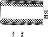
Fig. 5 A has represented the shape and the structure of various exemplary nozzle to the sectional view among Fig. 5 H;
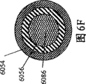
Fig. 6 A and 6B are the sectional view and the vertical views of an exemplary nozzle structure;
Fig. 6 C has represented various exemplary nozzle arrangements to the vertical view among Fig. 6 I;
Sectional view among Fig. 7 has represented to have a semiconductor processing equipment conductive member, exemplary;
Sectional view among Fig. 8 A and Fig. 8 B has also represented to have a semiconductor processing equipment conductive member, exemplary;
Fig. 8 C is the decomposition view of an exemplary wafer chuck assembly, and this chuck assembly has a conductive member;
Sectional view among Fig. 9 A and Fig. 9 B has represented to have a semiconductor processing equipment conductive member, exemplary;
Sectional view among Figure 10 A and the 10B has represented to have semiconductor processing equipment one and two optical pickocff, exemplary respectively;
Figure 11 A and Figure 11 B are respectively the vertical view and the sectional view of an exemplary semiconductor processing equipment;
Figure 12 is the sectional view of an exemplary semiconductor treatment facility;
Figure 13 A-13E has represented to have the exemplary electrolysis polishing assembly of a multichannel rotary components;
Sectional view among Figure 14 A and the 14B has been represented exemplary multichannel rotary nozzle assembly;
Figure 14 C has represented to be used for conductive layer on the wafer is carried out the example process of electropolishing;
Figure 15 is the sectional view of an electrolytic polishing chamber, and that this electrolytic polishing chamber has is exemplary, can linearly moving multichannel nozzle assembly; And
Figure 16 A-16E is the illustration figure of an electropolishing equipment, and this equipment has can linearly moving multichannel swivel nozzle.
Embodiment
In order to make the people to the present invention more thorough understanding be arranged, following description has been enumerated material, parameter of various concrete details features-for example concrete etc.But should be noted that: to the description of details is not to be for scope of the present invention is made qualification, and just for illustrative embodiments is done better to describe.
I. exemplary electropolishing equipment
Figure 1A and Figure 1B are a kind of sectional view and vertical views of exemplary wafer electropolishing equipment, and this equipment can be used to wafer 1004 is polished.More broadly, this exemplary electropolishing equipment is by metallic film, the while of electrolytic solution drainage on wafer carried out work to the wafer transport electric charge.Electric charge and electrolytic solution make the metal ion in the metallic film be dissolved in the electrolytic solution.Current density in the electrolytic solution and concentration of metal ions have determined the size of polishing speed at least on part.Thereby by the indexs such as concentration of current density, electrolytic solution are controlled, this electropolishing equipment just can accurately polish the metal level that is positioned on the semiconductor wafer.
Shown in Figure 1A, electropolishing equipment can comprise chuck 1002, actuator 1000 and polishing container 1008.Polishing container 1008 can be made with any non-conductive, acidproof corrosion-resistant material, and these materials for example are tetrafluoroethylene (commodity are called TEFLON), polyvinyl chloride (PVC), poly(vinylidene fluoride) (PVDF) and polypropylene etc.Preferably, polishing container 1008 can be made with PVDF.But should be noted that: can adopt different materials to make polishing container 1008 according to concrete application conditions.
Shown in Figure 1A, electrolytic solution 1038 can through nozzle 1010,1012 and/or 1014 and flow into the polishing container 1008 in.More specifically, pump 1020 is pumped into electrolytic solution 1038 in the strainer 1018 through reverse flow valve 1024 from electrolytic solution reservoir 1070.Strainer can comprise liquid mass flow director (LMFC), and this controller can be controlled the quantity and the flow of the electrolytic solution 1038 that flows to nozzle 1010,1012 and 1014.In addition, strainer 1018 can leach impurity from electrolytic solution 1038, so that reduce the amount that may enter into the impurity of polishing container 1008 through nozzle 1010,1012 or 1014, impurity may reduce the quality of electropolishing process, perhaps, if used LMFC, then impurity can block it.In a manner mentioned above, can prevent that impurity from entering into polishing container 1008 and/or blocking LMFC.In current embodiment, strainer 1018 can suitably be got rid of approximately the particle greater than 0.05 micron to 0.1 micron.But can recognize: can use various filtering systems according to concrete application.In addition, be useful although contaminant filter is fallen, in some application scenario, also strainer 1018 can be canceled from the wafer polishing assembly.
Pump 1020 can be that any suitable hydro-pump-for example is impeller pump, surge pump, bellows cylinder etc.In addition, pump 1020 can be acidproof, corrosion-resistant, and can tolerate impurity.Although only expressed a pump 1020 in the drawings, will be appreciated that: can use arbitrary number platform pump 1020.By way of example, can be each nozzle 1010,1012 and 1014 pump all is set individually.In addition, under some application conditions, electrolytic solution 1038 need not just can flow in the polishing container 1008 through nozzle 1010,1012 and 1014 by means of pump 1020.For example, the electrolytic solution in the electrolytic solution reservoir 1,070 1038 can be remained under the certain pressure.As alternatives, the line of pipes between electrolytic solution reservoir 1070 and nozzle 1010,1012 and 1014 is remained under the certain pressure.
LMFC can be any mass flow controller easily, and preferably, it also should tolerate acid, corrosion and impurity.In addition, LMFC carries electrolytic solution 1038 with the flow of setting to nozzle 1010,1012 and 1014.In addition, LMFC can come suitably conveying electrolyte 1038 according to the proportional flow of cross-sectional area with nozzle 1010,1012 and 1014.For example, if the diameter of nozzle 1012 greater than the diameter of nozzle 1014, then LMFC will be favourable with bigger flow to nozzle 1012 conveying electrolytes 1038.In current this exemplary embodiment, preferably: LMFC be designed to 0.5 liter/assign to 40 liters/minute flow electrolytic solution 1038 is carried out to be carried, concrete flux values depends on distance between the size of nozzle, nozzle and the wafer and other factor.
Electrolytic solution reservoir 1070 also can comprise a heat exchanger 1036, cooler/heater 1034 and a temperature sensor 1032, so that the temperature of convection cell reservoir 1070 electrolyte insides 1038 is controlled.In addition, one or more electrodes 1028 that link to each other with power supply 1030 can be set in reservoir 1070.Apply charge energy to electrode 1028 metal ion is removed from electrolytic solution 1038, come thus the concentration of metal ion in the electrolytic solution 1038 is regulated.Can in electrolytic solution 1038, add metal ion by apply opposite electric charge to electrode 1028.
This exemplary wafer polishing assembly also comprises the electrode that is arranged in nozzle 1012 and 1014.As hereinafter will introducing in detail,, also can use the electrode that is had in an arbitrary number nozzle and each nozzle, no matter and this number is greater than 2 or less than 2 although this exemplary embodiment has two nozzles that wherein have electrode.Generally speaking, the surface-area that adds electrode in the giant can increase current density, and can improve the electropolishing speed on the electrolytic solution 1038 stream longitudinal section transverse directions.
Shown in Fig. 1 D and Fig. 1 E, nozzle 1012 and 1014 has electrode 1056 and 1060 respectively.Electrode 1056 and 1060 can comprise any electro-conductive material-for example copper, stainless steel, tantalum (Ta), titanium (Ti), TaN, TiN, lead, platinum etc.
In the electropolishing process, some can accumulate on electrode 1056 and 1060 from the metal ion that the metal level of wafer 1004 moves out.As hereinafter will introducing in detail, can remove in the process of de-plating one metal accumulation horizon or coating are removed.For example, when applying negative charge when applying positive charge on electrode 1056 and 1060 on the wafer 1004, wafer is just electroplated but not by electropolishing.With similar mode, the metal that is plated on electrode 1056 and 1060 can be removed-promptly remove de-plating in this manner.As alternatives, can do suitable replacing according to any suitable duration counter electrode 1056 and 1060.For example, can just change electrode 1056 and 1060 after having handled about 100 wafers every.
In some instances, metal level can comprise copper product.Thereby in the electropolishing process, some cupric ions are moved on electroplated electrode 1056 and 1060 from just polished metal level.But if electrode 1056 and 1060 cuprics, then in removing the process of de-plating, electrode 1056 and 1060 will dissolve, thereby deforms.Thereby, in certain embodiments, wish in electrode 1056 and 1060 contained material can be in removing the process of de-plating resist dissolution.For example, electrode 1056 and 1060 can comprise platinum or platinum base alloy.As alternatives, electrode 1056 and 1060 can be the titanium that its outside is covered with one deck platinum, and the thickness of platinum layer is for example between 50 microns to 400 microns.
In this exemplary equipment, wafer chuck 1002 remains positioned in the container 1008 wafer 1004 or the top of container 1008 suitably.More specifically, wafer 1004 is being positioned properly, thereby faces nozzle 1010,1012 and 1014, and is arranged in sheath 1006.Sheath 1006 is optionally, and as hereinafter will introducing in detail, it is around wafer 1004, to prevent phenomenon such as splash.
After in wafer 1004 being properly positioned on polishing container 1008, apply electric charge to electrode 1056 and 1060 by power supply 1040.In addition, power supply 1040 also powers up to wafer 1004.As alternatives, also can adopt a plurality of power supplys come counter electrode 1056 and 1060 and wafer 1004 power up.If electric charge to apply situation suitable, then electrolytic solution 1038 will flow between electrode in nozzle 1012 and 1,014 1056,1060 and wafer 1004 surfaces, thereby has constituted circuit.More specifically, counter electrode 1056 and 1060 power up make its with respect to electromotive force of wafer 1004 for negative.In response to this negative potential on electrode 1056 and 1060, metal ion can be moved to the electrolytic solution 1038 from wafer 1004, thereby wafer 1004 has been carried out electropolishing.If but with the reversal of poles of circuit, then metal ion will move to wafer 1004, thereby wafer 1004 has been carried out plating.
In addition, shown in Figure 1A and Fig. 1 C, nozzle 1010 comprises injection nozzles 1052 and endpoint detector 1016.In the electropolishing process, but injection nozzles 1052 is designed to conveying electrolyte 1038, and endpoint detector 1016 then is designed to metal layer thickness on the wafer 1004 is detected.Endpoint detector 1016 can comprise the sonac of various transmitters-for example, optical reflection sensor, such as the electromagnetic sensor of current vortex sensor etc., and so on.The electrolytic solution 1038 that is transported by injection nozzles 1052 can be used as transmission medium, so endpoint detector 1016 sends signal through this medium, comes the thickness of metallic film is measured with this.Utilize electrolytic solution 1038 can improve the precision that endpoint detector 1016 is carried out measurement as the single medium of transmission signal, reason is that 1038 of electrolytic solution provide single material phase.In contrast, if injection nozzles 1052 is conveying electrolyte 1038 not, then from transmitting of sending of endpoint detector and measurement signal before passing the electrolytic solution 1038 that flows to wafer 1004 by nozzle 1012 or 1014, pass various other materials such as the air of medium-for example.As hereinafter will introducing, electrolytic solution 1038 is had can change in time in good time or real-time characteristic also can improve the precision of endpoint detector.In addition, have only a nozzle 1010 to have endpoint detector 1016, also can make an arbitrary number nozzle have an endpoint detector arbitrarily although be expressed as in the drawings.
Can find out also that from Figure 1A actuator 100 can rotate chuck 1002 and wafer 1004 around z axis.In addition, under some application conditions, actuator 1000 can move chuck 1002 and wafer 1004 along X-direction, and nozzle 1010,1012 and 1014 is kept motionless.In other application scenario, nozzle 1010,1012 and 1014 can move along X-direction, and that chuck 1002 and wafer 1004 keep on X-direction is motionless.Under other application conditions, actuator 100 can move chuck 1002 and wafer 1004 along X-direction, and simultaneously, nozzle 1010,1012 and 1014 also can move along X-axis.
In addition, can come this electroplating device is carried out orientation according to alternative form.For example, nozzle 1010,1012 and 1014 can be positioned at the top of wafer 1004, thereby make the electrolytic solution can be to down-wass to wafer 1004.In addition, wafer 1004 can be vertically oriented, and nozzle 1010,1012 and 1014 with the electrolytic solution drainage to wafer 1004.
Can be illustrated in No. 6395152 United States Patent (USP) of submitting on July 2nd, 1999, name is called " METHODS ANDAPPARATUS FOR ELECTROPOLISHING METALINTERCONNECTIONS ON SEMICONDUCTOR " and further understand this exemplary wafer electropolishing equipment, full content in the document all is incorporated into herein, with technology as a setting.In addition, can be illustrated in No. 6447688 U.S. Patent application of submitting on May 12nd, 2000, name is called " METHODS AND APPARATUS FOREND-POINT DETECTION " and further understand exemplary endpoint detector, the full content in the document all is incorporated into herein with as a reference.
II. the protection of splashing of electrolytic solution
A kind of exemplary electrolytic polishing method comprises operation: with electrolytic solution 1038 drainages in wafer 1004 surfaces, rotate wafer 1004.The slewing rate of wafer 1004 is enough to produce the centrifugal force that makes the electrolytic solution 1038 that is ejected on the wafer 1004 can flow to the edge in its surface.Preferably, electrolytic solution 1038 had been thrown to edge before under the drippage of wafer 1004 surfaces.By making electrolytic solution flow through the surface of wafer 1004, can prevent that fluid from dripping from wafer surface, thereby can not influence the jet that disturbs electrolytic solution 1038, perhaps prevented from container 1008, to form successive electrolytic solution drip fluid column.But such treatment process can cause electrolytic solution to splash in container, and splashes outside the equipment or disturb the jet of electrolytic solution.Thereby a kind of exemplary electropolishing equipment comprises a sheath 1006, and it overlaps around wafer 1004, is used for weakening or stops the liquid that is subjected to centrifugal action to splash in container 1008 or escape from container 1008 removing.
Figure 1A and Figure 1B have expressed sheath 1006, and it is designed to around wafer 1004 and chuck 1002.Shown in Figure 1A, nozzle 1012 can be to the surface transport electrolyte stream of wafer 1004.In order to polish the metallic film on the wafer 1004 more equably, can rotate wafer 1004 according to certain way, arrive the exposed parts place of chuck 1002 so that make electrolytic solution 1038 can flow through wafer 1004 but not drop onto the polishing container 1008 from the surface of wafer 1004.Any electrolytic solution that flows down and form successive electrolytic solution fluid column from wafer 1004 between wafer 1004 and polishing container 1008 all may cause the excessive polishing that wafer 1004 is formed the fluid column position.This extra polishing will cause the polishing speed of metal level inhomogeneous and unpredictable.
In addition, any electrolytic solution under wafer 1004 drippage or that splash in container 1008 all can disturb the electrolyte stream that is transported by nozzle 1012.Electrolytic solution 1038 effusive shapes-more specifically: effusive longitudinal section shape reverse comes to influence the polishing speed of current density and electropolishing equipment.Thereby, wish electrolytic solution 1038 along the surface current of wafer 1004 to the edge of wafer 1004, and away from electrolytic solution 1038 jets that are ejected on the wafer 1004.
Can rotate wafer 1004 according to suitable speed of rotation, so that electrolytic solution can flow through and flows to its edge or flow to the exposed parts of chuck 1002 from wafer 1004, concrete speed depends on the viscosity of used electrolytic solution.Velocity of rotation should make electrolytic solution 1038 flow through from wafer 1004, thus and the jet of can not go down formation successive fluid column or interference electrolytic solution 1038 from the surface drippage of wafer 1004.Specifically, the viscosity of electrolytic solution is low more, and needed centrifugal acceleration is high more.By way of example, the phosphoric acid for 85%, centrifugal acceleration is selected as surpassing about 1.5 meter per seconds
2In a kind of exemplary method, to diameter be the wafer rotation speed of 300mm at about 100 rev/mins (rpm) between about 2000rpm, even higher, preferably, at about 1500rpm between the 2000rpm.
Generally, nozzle 1012 or the 1014 whole surfaces with inswept wafer 1004 are so that polished wafer 1004 more equably.When nozzle 1012 was swept the different sites that is sprayed onto wafer 1004, the rotation of wafer 1004 should produce identical centrifugal acceleration on incident electrolytic solution 1038.For example, centrifugal acceleration be directly proportional with size apart from center wafer, with square being directly proportional of rotating speed.Thereby, if nozzle 1012 or 1014 is near the part at wafer 1004 edges-be that the long radius place carries out polishing, then the rotating speed of wafer 1004 just can reduce, and when the center time-radius that polishes the close wafer 1004 in position was very little, rotating speed just should increase.
Usually, if in a manner mentioned above to wafer 1004 conveying electrolytes, then electrolytic solution just can flow to the edge of wafer 1004, and cross the edge and flow to the polishing container 1008 sidewall.As sheath 1006 is not set, then electrolytic solution 1038 will touch the sidewall of polishing container 1008, thereby splashes in container 1008, can disturb the jet of electrolytic solution 1038 thus, perhaps can spatter to overflow from polishing container 1008 and go.
Shown in Figure 1A and Figure 1B, sheath 1006 can be placed with around wafer 1004 and chuck 1002, goes so that can weaken or prevent electrolytic solution 1038 splashing or spattering from container to overflow in polishing container 1008.In addition, in polishing process, sheath 1006 can move on the x direction of principal axis with chuck 1002 and actuator 1000.Specifically, can utilize mechanisms such as mechanical links, joint that sheath 1006 is connected on chuck 1002 and/or the actuator 1000.As alternatives, can use another actuator to drive sheath 1006 individually, this actuator is with the motion of sheath 1006 and the synchronized movement of chuck 1002 and actuator 1000.Sheath 1006 also can be consistent with chuck 1002 or be being rotated inconsistently.
Materials such as sheath 1006 usefulness plastics, pottery make, or use and make such as erosion-resisting metal or alloy such as tantalum, titanium, 300 series stainless steels.In addition, can on sheath, apply the material such as Teflon of the material that to resist electrolytic solution-for example.
But should be noted that: electrolytic polishing method mentioned above does not need electrolytic solution 1038 to flow through the edge of wafer and is splashed on the sheath 1006.Also flow through by halves under the situation of wafer 1004 at electrolytic solution, electrolytic solution 1038 will improve or solve with the problem that container 1008 forms continuous liquid columns, splashes in container 1008 or splashes outside the container 1008.For example, only design,, crossed the part of wafer surface, so just can weaken or prevent disadvantageous effect towards the marginal flow of wafer 1004 so that electrolytic solution is before under wafer 1004 drippage by rotation to wafer 1004.
III. reduce excessive polishing to the edge
On the other hand, hereinafter will electrolytic polishing method and the equipment that be used to reduce near position excessive polishing Waffer edge or the edge be described.Usually, the metal level of Waffer edge or vicinity, edge part is fallen by polishing quickly than the metal level of other location on the wafer.The electrode that is connected with Waffer edge can increase near the current density in the electrolytic solution wafer edge region, thereby causes the increase of polishing speed.In general, utilize one be arranged on the Waffer edge or the edge near conductive member sponge the one part of current density of passing through from electrolytic solution, just can reduce near higher current density and the polishing speed of wafer edge region, conductive member wherein for example is structures such as a ring body.Also can be by applying electric charge to conductive member, thus change its magnitude of current that absorbs and then realize control current density, just can adjust near the current density the edge to a greater extent thus.
Referring to Fig. 7, represented a kind of exemplary apparatus and method that reduces the edge excessive polishing among the figure.The liquid stream of electrolytic solution 7080 is ejected on the wafer 7004 from nozzle 7054.The velocity of rotation of wafer 7004 is enough to form an electrolytic solution thin layer 7081, and this thin electrolyte can be carried out polishing to the metal level on the wafer 7004.Generally, if the edge of wafer is connected with an electrode, then near the metal level on wafer 7004 edges or the edge is subjected to the speed of electrolytic solution thin layer 7081 polishings just faster than the metal level on wafer 7004 all the other zones.Therefore, the excessive polishing phenomenon will appear near the metal level wafer 7004 edges or the edge.
In addition, as shown in Figure 7, wafer 7004 can be positioned between wafer chuck 7002 and the conductive member 7114.For example device such as available mechanical arm is positioned at wafer 7004 near the position of wafer chuck 7002 or is located between wafer chuck 7002 and conductive member 7114.Then, can with wafer chuck 7002 and conductive member 7114 mutually near or compress so that wafer 7004 is remained between them.Thereby, this exemplary assembly can have other element, these elements for example are retainer or steady arm, they are used for wafer chuck 7002 is alignd with conductive member 7114, and the two is kept together, assembly also has some insulating components, and these members are at conductive member 7114 and between the contact element of wafer 7004 energisings.
Should be understood that: represented exemplary equipment also comprises other those parts shown in Figure 1A among Fig. 7, but under present case, these parts are omitted, so that to the description of this specific embodiment.By way of example, this exemplary equipment also can adopt sheath 1006 (seeing Figure 1A and Figure 1B) except having used elements such as various pumps, strainer, nozzle.
Fig. 8 A has represented to be used to reduce near the another kind of exemplary electrolysis polissoir of the polishing speed of Waffer edge.Expressed a chuck 8002 that has conductive member 8114 among the figure, conductive member wherein can reduce near the excessive polishing amount wafer 8004 edges or the edge.Fig. 8 A and Fig. 7 are similar, and difference only is that conductive member 8114 separates with wafer 8004 by a spacer element 8118.Spacer element 8118 for example is made of an O type circle.Also available other energy of spacer element 8118 is acidproof, corrosion-resistant insulation material is made, and these materials for example are pottery, tetrafluoroethylene (commodity are called TEFLON), polyvinyl chloride (PVC), poly(vinylidene fluoride) (PVDF), polypropylene, silicon rubber, viton etc.Conductive member 8114 links with power supply 8112, and one second conductive member or electrode (for example being spring member 8119) link with power supply 8110.As shown in the figure, can utilize the flow through electric current of conductive member 8114 of 8112 pairs of power supplys to regulate or control, so that near the polishing speed of metal level on wafer 8004 edges or the edge is controlled.In general, the magnitude of current that is absorbed along with bottom chuck 8114 increases, and the polishing speed of wafer 8004 edges or vicinity, edge metal level will reduce.
Similarly, conductive member 8114 also comprises such as metal or alloy such as tantalum, titanium, stainless steels, and other electro-conductive material.In addition, conductive member 8114 can comprise near the two or more segmental arcs that are arranged on wafer 8004 edges or the edge.
Thereby, in this exemplary electropolishing equipment, can utilize power supply 8110 and 8112 respectively the electric charge that flows to wafer 8004 through spring member 8119 and conductive member 8114 to be implemented separate control.Near the so just current density control wafer 8004 edges to a greater extent, and then control and reduce excessive polishing to fringe region.
Fig. 8 B is an enlarged view, has represented the structure and the annexation that are made of conductive member 8114 among Fig. 8 A and wafer 8004.Specifically, conductive member 8114 is powered by power supply 8112, and separates with wafer 8004 by spacer element 8118.Power supply 8110 powers up wafer 8004 individually, and this power supply is connecting with the spring member 8119 that positions around wafer 8004 edges.For example compare with the several electrodes of arranging along the edge of wafer 8004, the electric charge that is applied to wafer 8004 by spring member 8119 will distribute more evenly.Under the condition of separately powering, can an insulating component 8121 be set at conductive member 8114 and spring member 8119 by conductive member 8114 and spring member 8119.Spring member 8119 can be made as cyclic whisker (for example referring to Fig. 8 C), and still, the section profile of other shape-for example oval-shaped profiled outline also is feasible.In addition, can use the whisker of arbitrary number according to concrete application scenario.Can use any suitable elastic conducting material to make spring member, these materials for example are stainless steel, spring steel, titanium etc.Corrosion resistant materials such as also available platinum, TiN, TaN are made spring member 8119, or apply corrosion resistant material in the outside of spring member.
Can change contact point number between wafer 8004 and the power supply by the circle number of turns that changes in the spring member 8119.In this manner, the charge energy that flows to wafer 8004 distributes on the outer perimeter of wafer 8004 more equably, for example, for the wafer of 200mm specification, has applied about 1 to 10 ampere electric current usually.Spring member 8119 is designed,, so just the electric charge at each point of contact place can be reduced to about 1 to 10 milliampere so that be about 1000 with the point of contact of wafer 8004.
But should be noted that: also available one or more electric contact pieces are to wafer 8004 power supplies.In addition, it all is favourable adopting any measure that electric charge can be distributed around wafer 8004.
Being spaced apart between conductive member 8114 and the wafer 8004 under the condition that element 8118 separates, if spring member 8119 is exposed in the electrolytic solution, then short circuit will appear.Spring member 8119 short circuits may be reduced near the homogeneity of polishing speed wafer 8004 edge sections.Thereby in one embodiment, spacer element 8118 also plays the effect of sealing member, so that open spring member 8119 and electrolytic solution are isolated.Corrosion resistant materials such as available viton (fluorocarbon), silicon rubber are made spacer element 8118.In addition, can spacer element 8118 be made as different shape and structure according to concrete application conditions.
Fig. 8 C is a kind of decomposition view of exemplary wafer chuck retainer, this retainer and the above-mentioned supporting use of exemplary electrolysis polissoir that is used to reduce near the polishing speed of Waffer edge.This exemplary wafer chuck comprises a disk body, and the top of disk body has a basic component 8002, and has a conductive member 8114, and wherein, wafer 8004 is clamped between the basic component 8002 and conductive member 8114 of disk body.Wafer chuck also can comprise a top retainer (not shown), in order to wafer 8004 and chuck assembly cramping or remain to together.Except first conductive member 8114, wafer chuck also comprises one second conductive member, and it for example is a spring member 8119, and this member is used for powering up to wafer 8004.In certain embodiments, wafer chuck also can comprise insulating component 8121 and the spacer member 8118 that is arranged between basic component 8002 and the conductive member 8114, and conductive member 8114 wherein is positioned at the bottom of box body.But should be noted that: for example as shown in Figure 7, in some instances, spring member 8119 and spacer member 8118 can be removed.In the situation that spring member 8119 is cancelled, device such as an electrode can be set as second conductive member, be used for applying electric charge to wafer 8004.
In current example, spring member 8119 is disposed between wafer 8004 and the spring member 8118.If exert pressure conductive member 8114 is remained to basic component 8002, then spring member 8119 should keep and the electrically contacting of wafer 8004 (seeing Fig. 8 B).In addition, if necessary, spacer member 8118 is suitable for forming a sealing member between conductive member 8114 and wafer 8004, the sealing part can separate spring member 8119 and electrolytic solution, thereby realizes electrical isolation between spring member 8119 and conductive member 8118.
The shape of semiconductor wafer generally is substantially circle.Therefore, among the figure each building block of wafer chuck also is expressed as being roughly circle.But will be appreciated that: can each parts of wafer chuck be designed to different shape according to the shape of concrete application conditions and/or wafer.For example, semiconductor wafer can be circular for cutting, and the shape of each parts of wafer chuck should be consistent with it.
Be suitable for being used in aforesaid device and the method, be used for wafer is kept and can be referring to No. 6248222 United States Patent (USP) to its other representative configuration that applies the wafer chuck assembly of electric charge, the mandate day of this patent is June 19 calendar year 2001, name is called " METHOD ANDAPPARATUS FOR HOLDING AND POSITIONINGSEMICONDUCTOR WORKPIECES DURINGELECTROPOLISHING AND/OR ELECTROPLATING OF THEWORKPIECES ", and the full content of this patent all is incorporated into herein as a reference.
Fig. 9 A has represented to be used to reduce the another kind of exemplary electrolysis polissoir of Waffer edge near zone polishing speed.Particularly, as indicated above such, wafer chuck 9002 comprises the conductive member 9114 that can reduce near the excessive polishing amount of wafer 9004 edges or edge.Fig. 9 A and Fig. 8 category-A are seemingly distinguished and are that conductive member 9114 has a dead ring 9115 and the conducting ring 9116 in dead ring 9115.Dead ring 9115 can comprise such as erosion-resisting insulating material such as plastics, potteries.Conducting ring 9116 can comprise metal or alloy such as platinum, tantalum, titanium, stainless steel.Conducting ring 9116 can be connected with power supply 9110 by varistor 9112 devices such as grade.In addition, for example the spacer element 9118 for elements such as O type circles is placed between conductive member 9114 and the wafer 9004, is used to prevent that part by one or more electrodes and power supply 9110 comes in contact on electrolytic solution and the wafer 9004.In addition, device (not shown)s such as a spring member also can be set, so that electric charge is distributed on the wafer 9004 more equably.
Exemplary equipment makes the electro-conductive material that conductive member 9114 uses still less among Fig. 9 A.This just makes equipment more cheap, lighter, and consumes energy still less in the course of the work.In addition, than conductive member 8114 (seeing Fig. 8 A and 8B), the surface-area of conductive member 9114 is littler, so just can control the current density of wafer 8004 fringe regions on bigger degree.In addition, it will be favourable the structure among Fig. 9 A (and Fig. 7) and Fig. 7,8A being got up to use to the tectonic association of 8C.
Enlarged view among Fig. 9 B has been represented the another kind of example of electropolishing equipment.Equipment class among this embodiment and Fig. 9 A seemingly, difference is to be shaped on an insulating component 9121 on the opposite side of the bottom of conductive member 9114-promptly and wafer 9004.In addition, the structure of wafer assemblies is designed to: make that the metal level 9005 on the wafer 9004 is to obtain electric charge by a spacer member 9118 of conducting electricity in submarginal position.
Thereby shown in Fig. 9 B, electrolytic solution 9080 is diversed to the position near wafer 9004 edges, thereby makes one part of current I
1Flow to metal level 9005, the second section electric current I
2Flow to conductive member 9114.Insulating component 9121 on conductive member 9114 bottoms is used to reduce electric current I
2Thereby, increase the electric current I that flows to metal level 9005
1Thereby, can come electric current I by the relative thickness of adjusting insulating component 9121 and conductive member 9114
1And I
2Do corresponding the adjusting.
IV. metal level broken on the wafer is carried out the method for electropolishing.
In the electropolishing process, the metal level that forms on the wafer may become broken shape.For example, one or more discontinuous metallic region may can appear on wafer surface.If such situation, then some metal fragment just may with wafer on be provided with electrode the edge disconnect.In the case, owing to electrode can not power up the metal level of fragmentation, so traditional electrolytic polishing method just can't partly be disposed these fragments effectively.In a kind of exemplary method, by with sufficiently high rotational speed wafer, and around the fragment part of metal level, a conductive member is set, just can be on the fragment part formation skim electrolytic solution, this layer electrolytic solution contacts with conductive member.Electrolytic solution thin layer and conducting ring make that fragment partly becomes can be by electropolishing.
Shown in Figure 11 A and Figure 11 B, the metal level 11150 among the figure has for example become broken shape in polishing process.The fragment of metal level 11150 is not connected with the edge of wafer 11004 or is positioned on the edge, and in edge, an electrode (not shown) is being connected with power supply 11110.Because the fragment of metal level 11150 is not in the edge of wafer 11004 or couples together by means of metal and edge, arrives the electrode of wafer 11004 edges so electric current can't be flowed through fragment.Thereby, traditional finishing method-for example wafer is immersed in the medium method of polishing trough generally can't polish to these fragments.
The fragment 11150 of metal level for example is some exposed barrier layer portions, the copper layer is polished go after, these barrier layer portions are still stayed on the non-channel part of semiconducter device.In addition, metal level fragment 11150 for example also may be the result of or excessive polishing inhomogeneous to the polishing of fringe region.
Referring to Figure 11 B, represented a kind of exemplary apparatus that is used for the metal level fragment on the wafer 11004 is carried out electropolishing among the figure.This polishing system comprises chuck 11002, fixed nozzle 11054 and power supply 11110.Such as mentioned above, at nozzle 11054 during to the liquid of wafer 11004 jet electrolytic liquid 11080 stream, actuator 11000 drives chuck 11002 and rotates, thereby electrolytic solution 11080 is flowed on the surface of wafer 11004, formed a thin layer 11081 therefrom, the casual fragment part of having flooded metal level 11150 of this thin electrolyte.By way of example, for the wafer of 300mm diameter, the rotating speed of wafer chuck 11002 in the scope of 2000rpm, is preferably about 1500rpm about 100rpm.Electrolytic solution thin layer 11081 has formed a path of passing metal level 11150 fragments so that between the conductive member 11114 of electrolytic solution jet 11080 and chuck 11002 conduction current.This electric current makes equipment carry out electropolishing to isolated metal level fragment 11150 on the wafer 11004.
In addition, the exemplary apparatus shown in Figure 11 B can be an integral part of the large-scale electrolysis polishing assembly of assembly shown in Figure 1A etc.For example, a sheath 1006 (see figure 1)s can be set prevents and splashes, polishes uneven or the polishing fluid stream of electrolytic solution 1038 is caused interference.In addition, can with above-described, be applied on the equipment shown in Figure 11 B about the various illustrative embodiments of the conductive member 11114 that reduces edge polishing speed.
Figure 12 has represented to carry out metal level fragment on the wafer 12004 the another kind of system of electropolishing.Figure 12 and Figure 11 are similar, difference only be actuator 12180 and 12182 can be in the locational chuck 12002 of actuator 12000 rotational fixation, nozzle 12054 is moved along X-axis.
Although in Figure 11 B and system shown in Figure 12, chuck or nozzle are to move along X-direction, will be appreciated that: no matter be chuck, or nozzle can move on indefinite direction according to concrete application conditions.
V. metal concentration is measured and end point determination control
Under the environment of producing in batches, make the quality of finish of wafer stable and consistent and be exactly more: the metal concentration in the source of supply of the used electrolytic solution of polished wafer is controlled in a factor can accepting in the limit.If the metal concentration in the electrolytic solution source of supply reaches certain value, then the activity of electrolytic solution will be very high-even under the situation that does not apply any electric current.In the treating processes after electropolishing, such situation for example can cause chemical milling or the corrosion to wafer.Thereby hope can be monitored the metal concentration in the electrolytic solution in the course of the work, and can regulate concentration on real-time basis as required.
In addition, the end point determination transmitter generally is to adopt optical pickocff, and it penetrates electrolytic solution and measures.Thereby measuring result depends on the optical characteristics of electrolytic solution at least on part.But the optical characteristics of electrolytic solution can change in time, and changing condition depends on that metal is added to concentration in the electrolytic solution and other factor, and other factor for example is hydrogen gas bubbles that forms in impurity particle, the electrolytic solution etc.Thereby, because in the implementation of technology, the optical characteristics of electrolytic solution can change, thus to correspondingly regulate from the measuring result of endpoint detector output, so that improve end point determination result's precision.
Figure 10 A has represented a kind of exemplary system, and it can be used to the metal concentration in electrolytic solution 10038 sources of supply is measured, and source of supply wherein for example is electrolytic solution reservoir 1070 devices such as (seeing Figure 1A).This exemplary system comprises fibre-optical probe 10102, Fibre Optical Sensor 10104 and reverberator 10100.Fibre-optical probe 10102 and reverberator 10100 are immersed in the electrolytic solution 10038, fibre-optical probe 10102 can position with respect to reverberator 10100, so that make light that fibre-optical probe 10102 sends with the light intensity of the maximum device 10100 reflected back optical fiber probe 10102 that is reflected.By way of example, shown in Figure 10 A, fibre-optical probe 10102 can be oriented to along the direction emission light perpendicular to reverberator 10102 surfaces.
In addition, the distance H between reverberator 10100 and the fibre-optical probe 10102 may have influence on the precision to metal concentration measuring result in the electrolytic solution.Thereby the H that adjusts the distance selects, so that optical pickocff 10104 receives maximum light intensity can reach minimum value in the concentration in electrolytic solution 10038 sources of supply time.Should be noted that: can select other path of optical pickocff 10104 and reverberator 10100, can select route for use according to concrete application conditions and desirable path length with multistage path and multiple reflection.Fibre-optical probe 10102 also can be set at the outside of electrolytic solution reservoir, thereby makes travel path cross a part of electrolytic solution 1038.In addition, can utilize an optical pickocff to replace reverberator 10100, this optical pickocff is configured to and can the light intensity that be received by optical pickocff 10104 be detected.
In general, the color of electrolytic solution depends on type and the concentration that is added to the metal ion in the electrolytic solution.By way of example, cupric ion is at phosphoric acid (H
3PO
4) in be blue.In addition, pass the color that light intensity attenuation behind the electrolytic solution depends on electrolytic solution.Generally, along with the raising of metal ion concentration in electrolytic solution, the decay of light intensity is also being strengthened.
For the system shown in Figure 10 A, at employed special metal of this system and electrolytic solution, the relation in the electrolytic solution between metal concentration and the light intensity attenuation is programmed in the following table:
| Metal concentration (wt%) | Light intensity attenuation |
| 0 | Y1 |
| 0.2 | Y2 |
| 0.4 | Y3 |
| 0.6 | Y4 |
| 0.8 | Y5 |
| 1.0 | Y6 |
This list information can be stored in the computer 10105.Computer utilizes this list information, according to by optical pickocff 10104 detected light intensity values, uses interpolation, rounding or other suitable algorithm to calculate metal concentration in the electrolytic solution automatically.Although listed some special values in the superincumbent form, can use any numerical value, and can use any a plurality of concentration value about metal concentration (wt%).
Can select the color of the light launched by fibre-optical probe 10102, so that improve the sensitivity of optical pickocff 10104 detected measuring results.Specifically, the color of the light of being launched by fibre-optical probe 10102 can be different from the color of metal ion in the electrolytic solution source of supply, so that improve this special metal ionic sensitivity.For example, for the cupric ion in phosphoric acid, the sensitivity in the time of will being higher than transmitting green light to the sensitivity of cupric ion during red-emitting, and the sensitivity of the sensitivity during green glow when being higher than the emission blue light.But for the metal ion of any color in the electrolytic solution, white light all is fine.
Figure 10 A has also expressed an above-mentioned example system on the other hand, and this system can be used to metal ion is got rid of from the source of supply of electrolytic solution 10038.This system also comprises two electrodes 10028 and 10029 and power supply 10030.When optical pickocff 10104 is measured concentration of metal ions in electrolytic solution 10038 sources of supply and has been reached one first preset value, computer 10105 just sends instruction to power supply 10030, make it apply voltage, so that metal ion is got rid of from the electrolytic solution source of supply to electrode 10028 and 10029.When electrode 10028 and 10029 applies voltage, the metal ion that comes from electrolytic solution 10038 sources will be coated on the electrode 10029.If detecting concentration of metal ions, optical pickocff 10104 dropped under one second preset value, computer 10105 just indicates power supply 10030 to stop to apply voltage to electrode 10028 and 10029, thereby stops to remove metal ion from electrolytic solution 10038 sources.In such a manner, for example in the electropolishing process, the concentration of metal ion in electrolytic solution 10038 sources of supply can be remained between first preset value and second preset value.
The concentration value of metal ion also is helpful for endpoint detector 1016 (seeing Figure 1A, 1B) in the electrolytic solution 10038.Endpoint detector 1016 can be used to determine metal layer thickness on the wafer 1004.This information of electropolishing equipment utilization determines when the electropolishing process that continues on execution or the termination wafer 1004 a certain specific regions.Also can utilize this information to determine suitable polishing speed.Endpoint detector 1016 can comprise various transmitters, for example sonac, optical pickocff, electromagnetic sensor etc.Utilize electrolytic solution 1038 can improve the precision of measuring result as the medium that transmits the signal and the measuring result that obtains, reason is to consider that the air of interface-for example between the medium is to the interface of electrolytic solution 1038.But if change has taken place electrolytic solution 1038 those characteristics that can have influence on transmitter, then measuring result just can not keep correct in time.Thereby, by the characteristic changing factor of electrolytic solution 1038 is taken into account, just can improve the result of endpoint detector.
Figure 10 B has represented another kind of exemplary system, and it is used to monitor the optical characteristics of electrolytic solution, for example utilizes optical characteristics to come the detected result of endpoint detector is adjusted.Figure 10 B and Figure 10 category-A are seemingly distinguished and only are to be provided with one second optical pickocff 10204 and optical fiber 10202.The mode of operation of optical pickocff 10104, optical fiber 10102 and reverberator 10100 is identical with reference to the described mode of Figure 10 A with the morning.The principle of work of second optical pickocff 10204 and optical fiber 10202 also is similar to optical pickocff 10104 and optical fiber 10102; But optical pickocff 10204 is other optical characteristics of electrolytic solution with optical fiber 10202 measurements.For example, in the process of carrying out electropolishing, can on electrode, form hydrogen gas bubbles usually.Bubble is owing to can reflect in the electrolytic solution measuring beam and reduce its intensity, so can have a negative impact to endpoint detector.The reduction of measuring beam intensity can have influence on the measuring result of concentration of metal ions, still, by adopting a plurality of detectors to the different qualities sensitivity, just can accurately determine the concentration of metal ion.
In this embodiment that the optical characteristics that electrolytic solution is occurred by bubble is determined, equally the color of fibre-optical probe 10202 emitted lights is selected, to improve sensitivity by optical pickocff 10204 detected measuring results.In the case, the color of 10202 isolychns of fibre-optical probe can be elected as with the electrolytic solution source of supply in the identical color of metal ion, thereby can improve sensitivity to bubble, and reduce sensitivity to metal ion.For example, for the copper in the phosphoric acid supply liquid, the emission blue light has higher sensitivity than the emission white light to bubble, but then lower to the sensitivity of cupric ion, and the emission white light is compared with red-emitting, and is higher to the sensitivity of bubble, lower to the sensitivity of cupric ion.
In addition, any bubble that occurs in the electrolytic solution all can weaken the intensity of fibre-optical probe 10102 ruddiness that sends, thereby makes the measuring result of copper ion concentration inaccurate.But it mainly is to be subjected to aeration but not influenced by copper ion concentration and the light intensity part that reduces that second optical pickocff 10204 can indicate, and reason wherein is that it is insensitive that the susceptibility of fibre-optical probe 10202 is chosen to be copper ion concentration.Thereby, take into account by reducing part by second optical pickocff, 10204 light intensity that determine, that be subjected to aeration, just can determine weakening of red light intensity.In addition, endpoint detector 1010 (seeing Figure 1A) can be found out the optical characteristics of electrolytic solution from computer 10105, and accurately measures the metal thickness on the wafer 1004 (seeing Figure 1A).Thereby second optical pickocff 10204 can improve the precision of endpoint detector measuring result, also can improve the precision to the concentration of metal ions observed value.
Should recognize: can use the transmitter of arbitrary number to come every characteristic of electrolytic solution is measured.The optical characteristics of various characteristics-for example etc. can be stored, and is used for the observed values such as measuring result of endpoint detector are regulated or determined.
VI. the structure of nozzle
According to a further aspect, be used for a kind of illustrative methods of metallic film execution electropolishing on the wafer is comprised measure with equipment: adopt polishing speed nozzle different, multiple size.In general, big nozzle is higher to the polishing speed of the metallic film (for example copper film) that forms on the wafer, and the polishing speed of small nozzle is just lower.Thereby available giant comes metal level is carried out rough polishing, then, adopts small nozzle to come more accurately to control the electropolishing process.Thereby for the situation that will carry out accurate more polishing to the wafer different zones, it will be favourable adopting a plurality of nozzles.But, for example because the size in the available space is limited, so wish to have the equipment energy compactness of a plurality of nozzles.A kind of exemplary equipment has realized using the design of a plurality of nozzles in tight space, this equipment has the nozzle of certain number, and these nozzles are arranged on the nozzle holder of a rotation.
Figure 13 A, 13B, 13C, 13D and 13E have represented a kind of exemplary electrolysis polishing assembly with a plurality of rotating nozzle assemblies.Figure 13 A is similar to Fig. 1 E to Figure 13 E and Figure 1A, and difference only is: in the position near optical endpoint detection device 1014, other has added a rotating nozzle 1012 with a plurality of nozzles, and has set up current vortex thickness/endpoint detector 1009.Shown in the arrow among Figure 13 A, swivel nozzle 2012 can rotate, thereby the nozzle 1014 of different size and/or shape is positioned to guide the jet of electrolytic solution 1038 into wafer 1004.Thereby pump 1018 is just given endpoint detector 1016 pairing nozzle 1010 and single-nozzles 1014 with electrolytic solution 1038 pumpings, and in Figure 1A, 1038 of electrolytic solution are transported in each the independent nozzle that is adopted.
Like this, swivel nozzle 2012 just can be rotated according to the thickness and the other factors of the part that will be carried out polishing on the wafer 1004, metallic film, to select a required nozzle 1014.For example, in the very thick location of metal level, use big nozzle, and, then will use small nozzle in the very thin zone of metal level.Thereby the nozzle that a plurality of different sizes and profile are set in simple, the compact electropolishing assembly that an energy is more changed quickly and easily can improve the precision of polishing operation.
Referring to Figure 14 A, represented a kind of cross-section structure of exemplary multichannel rotating nozzle support 2012 among the figure.Swivel nozzle support 2012 is keeping injection nozzles 2014.Drive unit 2070 is rotating swivel nozzle 2012 by means of drive sub 2068, in order to locating a new injection nozzles, so that to the jet channeling conduct of electrolytic solution.One O type circle 2066 for example seals drive sub 2068.Drive unit 2070 can be the devices such as wheelwork of stepper-motor, servomotor, pneumatic (pressurized gas or liquid) driving.Injection nozzles 2014 on the swivel nozzle support 2012 has electrode 2056, and this electrode links with external power source (seeing Figure 13 A) by current feed 2062.Rotating nozzle support 2012 is landed on the plate 2084, and it is by O type circle 2072 and bolt 2074 and sealing with polishing room 1008.
Plastics such as nozzle holder 2012 usefulness PVC, PVD, TEFLON, polypropylene are made, or are covered with insulation and corrosion-resistant material basically outward.Nozzle 2014 can be made with materials such as tantalum, titanium, platinum, stainless steels.
Figure 14 C has represented to utilize the equipment shown in Figure 14 A that the metallic film on the wafer 1002 is carried out a kind of example process that electropolishing is handled.In step 1, determine the profile of thickness of metal film, this operational example is as indicated above in this way to be finished like that: when wafer 1004 rotates, endpoint detector 1009 translation on X-direction.In step 2, can use a giant 2014, metallic film be carried out initial burnishing with higher polishing speed.After adopting high polishing speed, in step 3, swivel nozzle 2012 is rotated, so that use small nozzle 2014, carry out work with lower polishing speed.After initial burnishing through step 1 and/or step 2, in step 4, utilize endpoint detector 1009 to determine the profile of residual metallic thickness, endpoint detector wherein for example is devices such as current vortex endpoint detector, optical endpoint detection device.In step 5, profile based on the residual metallic thickness of determining by step 4, the polishing electric current is regulated or adjusted, so that polishing is carried out at the thick film position with higher polishing speed, and polishing is carried out at the film position with lower polishing speed, and be zero position at film thickness, then stop to carry out polishing.For example can just can adjust by using the power supply of different nozzles 2014 and/or change power supply to the polishing electric current.In step 6, repeat measurement to thickness profile-be step 4, if metal layer thickness has reached a preset value, then just stopped the execution of polishing process.But if the thickness of metal preset value not as yet, then repeated execution of steps 5, directly cause to reach till the ideal thickness.
Should recognize: can do multiple change and variation the process shown in Figure 14 C.In addition, the exemplary apparatus shown in also available Figure 14 A is finished numerous other processing.
Referring to Figure 14 B, represented another kind of exemplary multichannel rotary nozzle assembly among the figure.Nozzle assembly shown in rotary nozzle assembly shown in Figure 14 B and Figure 14 A is similar, and difference only is that drive sub 2068 is replaced by magnetic coupling joint 2078 and 2082.Adopt magnetic coupling joint 2078 to be with an advantage of 2082: drive sub 2078 directly is not connected with nozzle holder 20122066, and can cancel the O type circle among Figure 14 A.This can reduce the possibility that electrolytic solution 1038 leaks into drive sub 2068.Thereby as can be seen: the whole bag of tricks that drive sub 2068 is connected on the swivel nozzle 2012 all is feasible.
Referring to Figure 15, represented among the figure a kind of can linearly moving multichannel nozzle assembly.Except realizing the motion of translation opposite with rotational motion, working process and Figure 13 A that this can linearly moving multichannel nozzle assembly are similar to the working process of swivel nozzle 2012 shown in Figure 13 E.This linear movable nozzle assembly comprises respectively nozzle 3054, the nozzle 3222 and 3226 with electrode 3056,3220 and 3224.These three nozzles are designed to have different profiles, for example have different diameters, thereby different polishing speeds can be provided.
Utilizing nozzle holder 3180 and moving guide rail 3182, nozzle 3054,3222 and 3226 can be in the horizontal direction-and be to move on the X-direction.Electrode 3056,3220 also is connected with power supply 3110 by the lead-in wire (not shown) with 3224.Electrolytic solution 3080 is flowed through nozzle holder 3180 and is transported in nozzle 3054,3222 and 3226.Described like that with reference to Figure 14 C as mentioned, be used for using the nozzle 3054,3222 and 3226 of each different size interchangeably in execution from the electropolishing process of wafer 1004 removal metallic membranes.In general, when metallic film was very thick, available giant was carried out polishing with higher polishing speed to metallic membrane, and if metallic membrane is very thin or only wish to remove very a spot of metal, then available small nozzle is carried out polishing with lower polishing speed to metallic membrane.
Figure 16 A has represented a kind of exemplary electropolishing assembly to Figure 16 E, and it comprises a multichannel rotary nozzle assembly.Except other added one can linearly moving base 4180 and moving guide rail 4182, Figure 16 A is similarly to Figure 16 E and Figure 13 A to Figure 13 E, wherein, swivel nozzle 4012 and 4014 is installed on guide rail 4182.
Specifically, multichannel swivel nozzle 4014, optical endpoint detection device 4016 and thickness/terminal point current vortex detector 4060 be installed to can linearly moving base 4180 on.Linear movable substructure member can along moving guide rail 4182 in the horizontal direction-be to move on the X-direction.This assembly makes the multichannel nozzle can be installed in the compact space.
The structure of multichannel nozzle 4014 and principle of work are all similar to situation shown in Figure 14 B with Figure 14 A, still, for the ease of expression, have omitted such as structures such as rotating driving device, drive sub, current feed and electrolytic solution pipelines among the figure.
VII. the automatically cleaning process of nozzle
According to a further aspect in the invention, a kind of self-cleaning method of electropolishing nozzle that is used to make hereinafter will be described.In common electropolishing technology, the metal that is added in the electrolytic solution may be coated on the injector electrode gradually.Be coated with the perforate that the metal that is covered with may limits nozzle or make the perforate distortion, thereby changed electrolytic solution effusive shape and/or direction.The change of liquid stream shape can cause that current density changes in the liquid stream, thereby can change the careless polishing speed of electropolishing.By apply a reverse voltage to nozzle, can carry out de-plating to nozzle and handle or clean, wherein, the reverse voltage that is applied can impel metal ion to be added in the electrolytic solution once more.For example, this metal can be electroplated onto on another nozzle, an expendable material or other object.
Refer again to Figure 1A to Fig. 1 E, polished the metal that gets off from wafer 1004 metal levels can be added to the electrolytic solution 1038, and can cause Metal plating that a part dissolves on injector electrode 1056 and/or 1060.For metal is got rid of from injector electrode 1056 and/or 1060, can apply a reverse voltage to injector electrode 1056 and/or 1060.No matter be the DC power supply, or AC power supplies all can be used to apply reverse voltage.In a kind of exemplary method, applied reverse voltage and be added in the electrolytic solution piling up the metal that gets up.In the exemplary method of another kind, the reverse voltage that is applied is on Metal plating to the disposable wafer that accumulation is got up.In another example, the reverse voltage that is applied with the Metal plating of pile up to a block.
A. utilize the DC power supply that the metal accumulation thing is added in the electrolytic solution.
Referring to Figure 1A, utilize a DC power supply, can get off and be added in the electrolytic solution 1038 being deposited in electrolytic etching of metal on the nozzle 1012.More specifically, lead C is connected on the lead b, lead B is connected with lead a, thereby just injector electrode 1056 (is seen Figure 1B-1E) as anode, and injector electrode 1060 has been used as negative electrode, can be to nozzle 1012 and 1014 conveying electrolytes 1038, so that between electrode 1056 and 1060, form circuit, this just makes that the metal that is deposited on the nozzle 1012 can be removed from this nozzle, and is added in the electrolytic solution 1038.The a part of metal that is added in the electrolytic solution 1038 can be electroplated onto on the nozzle 1014.
As if just metal is removed and is electroplated onto on another nozzle from a nozzle although seem this treating processes, still stay the electrolytic solution 1038 from most of metal that nozzle 1012 is removed.For exemplary electropolishing process, in the electrolytic solution 1038 concentration of metal generally lower-for example less than 3% (weight ratio), thereby the electropolishing process is to be started by charged electrode 1012 and 1014, but not is that chemical property by electrolytic solution 1038 drives.Thereby the amount of metal that gets off from nozzle 1012 electrolysis is greater than the amount of metal that is electroplated onto on the nozzle 1014.For example, whenever remove following 10 metal ions from nozzle 1012, just have a metal ion to be electroplated onto on the nozzle 1014, this just causes most of metal ion to be dissolved in the electrolytic solution 1038.
Continuation can utilize a DC power supply to carry out this process conversely, thereby the electrolytic etching of metal that will be deposited on the nozzle 1014 is fallen, and it is dissolved in the electrolytic solution 1038 with reference to Figure 1A.More specifically, lead B is connected with lead b, and lead C then is connected with lead a, thereby makes injector electrode 1060 (seeing that Figure 1B is to 1E) become anode, and with injector electrode 1056 as negative electrode.To nozzle 1012 and 1014 conveying electrolytes 1038, so that form circuit, this circuit makes the metal that is deposited on the nozzle 1014 be added to the electrolytic solution 1038 from this nozzle.Equally, also some metal that is added in the electrolytic solution 1038 is electroplated onto on the nozzle 1012.
By repeating the voltage of nozzle used in above-mentioned process-promptly converse repeatedly this equipment, just can finish clean operation to nozzle.In an exemplary process, when wafer is carried out electropolishing successively, at first be nozzle 1012 to be carried out de-plating handle, nozzle 1014 carried out electroplated, back time operation is then carried out de-plating to nozzle 1014 and is handled, nozzle 1012 is carried out electroplated, and comes to clean apace two nozzles thus.As discussed above such, because than the amount of metal that is electroplated onto on the relative nozzle, most of metal has been added in the electrolytic solution 1038, so in fact two nozzles can obtain cleaning.
Fig. 2 and Fig. 3 have represented nozzle 1012,1014 residing two kinds of exemplary status in cleaning course.Nozzle 1012,1014 is oriented to close mutually, and electrolytic solution is flow through from nozzle 1012,1014, thereby forms an electrolyte membrane or a runner between them.A time-out-as shown in Figure 3, then two-layer electrolyte membrane of mobile or runner 1080 will be merged together and form single flow channel between nozzle 1012,1014 when nozzle 1012,1014 is arranged to come to.This single flow channel has shortened the length of circuit, thereby has improved the elimination efficiency to the metal accumulation thing.Certainly, therefrom should be able to find out: this exemplary method also can be used for nozzle more than two situation.
B. utilize the DC power supply that the metal accumulation thing is electroplated onto on the wafer
Referring to Figure 1A, according to another kind of exemplary process method, the electrolytic etching of metal that adopts a direct current power supply will be deposited on the nozzle 1012 falls, and it is electroplated onto on the wafer 1004.More specifically, lead A is connected with lead b, and lead B then is connected with lead a, thus with wafer 1004 as negative electrode, and injector electrode 1056 (is seen that Figure 1B-1E) has been used as anode.Electrolytic solution 1038 is carried to wafer 1004 from nozzle 1012, thereby has formed a closed circuit, so just can will be deposited in Metal plating on the nozzle 1012 to wafer 1004.After metal on will being deposited in nozzle 1012 is disposed, wafer 1004 can be abandoned.
Similarly, referring to Figure 1A, also the electrolytic etching of metal that can utilize direct supply will be deposited on the nozzle 1014 falls, and it is electroplated onto on the wafer 1004.More specifically, lead A can be connected with lead b, lead C then is connected with lead a, thus with wafer 1004 as negative electrode, and injector electrode 1060 (is seen that Figure 1B-1E) has been used as anode.Electrolytic solution 1038 is carried to wafer 1004 from nozzle 1014, thereby forming circuit so just can will be deposited in Metal plating on the nozzle 1014 to wafer 1004.Nozzle in the electropolishing equipment 1012 or other nozzle can be carried out parallel connection with nozzle 1014 or connect, so that obtain cleaning.After metal on will being deposited in nozzle 1014 is disposed, wafer 1004 can be abandoned.
C. utilize a DC power supply that the metal accumulation thing is electroplated onto on the block
Referring to Fig. 4, the method exemplary according to another kind utilizes direct supply with metal accumulation thing 1057 electrolytic dissolutions on the nozzle 1012, and it is electroplated onto on the block 1082.More specifically, lead B is connected with lead a, and lead D then is connected with lead b, thus with block 1082 as negative electrode, and injector electrode 1056 has been used as anode.Electrolytic solution 1038 (see figure 1)s were carried from nozzle 1012, and can contact with block 1082, thereby had constituted a closed circuit through electrolytic solution 1038, made the metal that is deposited on the nozzle 1012 can be electroplated onto on the block 1082.After metal on will being deposited in nozzle 1012 is disposed, block 1082 can be abandoned.
Similarly, referring to Fig. 4, metal accumulation thing 1057 electrolysis that also can utilize direct supply will be deposited on the nozzle 1014 are fallen, and it is electroplated onto on the block 1082.More specifically, lead C can be connected with lead a, lead D then is connected with lead b, thus with block 1082 as negative electrode, and injector electrode 1060 has been used as anode.Electrolytic solution 1038 (see figure 1)s were carried from nozzle 1014, and can contact with block 1082, thereby had constituted a closed circuit, and this circuit can will be deposited in Metal plating on the nozzle 1014 to block 1082.After metal on will being deposited in nozzle 1014 is disposed or when an opportunity arises, block 1082 can be abandoned at other.In addition, electrode 1056 and 1060 can be together in series or be together in parallel and carry out cleaning.
D. utilize AC power to remove the metal accumulation thing.
In the exemplary nozzle cleaning method of another kind, can in any above-mentioned structure, adopt the AC power opposite to come to get rid of the metal accumulation thing from nozzle 1012 and 1014 with direct supply.Specifically, an AC power supplies is used for the metal accumulation thing is dissolved into electrolytic solution, and the metal accumulation thing is electroplated onto wants on abandoned wafer, block or other expendable material.
Concentration of metal is low more in the electrolytic solution, and the efficient of the metal accumulation thing being got rid of from nozzle with AC power supplies is high more.Therefore, when carrying out the removing operation, metal concentration generally is in the scope of about 0.1% to 5% (weight ratio), preferably approximately less than 0.5%wt.
VIII. its shape of nozzle
In any above-mentioned illustrative embodiments, can both advantageously use the nozzle of different shape.Different types of nozzles-for example the nozzle of different size, different profile, varying cross-section shape etc. can bring different polishing characteristics, can advantageously select these nozzles for use according to concrete application feature.For example, shown in Figure 1B, exemplary electropolishing equipment comprises the nozzle 1012,1014 of two different sizes among the figure, and these two nozzles are used to the different sites of wafer 1004 is carried out electropolishing.
In addition, Fig. 5 A has represented to have the exemplary nozzle of different shape and structure to Fig. 5 H.Its passage of its shape of nozzle-for example and its far-end can change the current density from the effusive electrolyte flow state of this nozzle, electrolytic solution jet etc.Fig. 5 A has expressed various structure and the shapes that have the nozzle of isolator 5054 and electrode 5056 to Fig. 5 E.Fig. 5 F has represented the various nozzles that do not have isolator to Fig. 5 H.The nozzle of some structure has the meander electrode 5056 near its opening.Crooked electrode 5056 can prevent from the spike electric charge to occur at the cusp place of electrode, and this will help to make current density more even in the liquid stream of electrolytic solution.Fig. 5 H has represented a kind of nozzle that has the electrode 5056 and a body of rod 5058, and the body of rod 5058 approaches the center of nozzle, and it is used to increase the surface-area of electrode, thereby makes current density become more even.
For each said nozzle, electrode 5056 all comprises such as metal or alloy such as tantalum, titanium, stainless steels.In addition, isolator 5054 can comprise plastics such as PVC, PVD, Teflon, or Al
2O
3, ZrO
2, SiO
2On pottery.Therefore, because metal and alloy are easier to be made as different shape than plastics and pottery usually, so than other shape, the cost of making the nozzle that has bending or taper electrode and vertical bar shape isolator is lower.In addition, nozzle shown in Fig. 5 F, 5G and 5H, that only have an electrode 5056 has more simple structure design and bigger surface-area.In addition, the nozzle shown in Fig. 5 H has a body of rod 5058, and it can make electrode have bigger surface-area as the integral part of electrode 5056, thereby can make the Potential Distributing on the electrolytic solution 1038 (see figure 1) sections of crossing from nozzle flow more average.The more uniform electromotive force that distributes makes to be handled more even to the electropolishing of wafer 1004.
Fig. 6 A and Fig. 6 B have represented another kind of exemplary nozzle, and it has the internal structure 6086 of isolator 6054, electrode 6056 and conduction.Internal structure 6086 comprises such as metal or alloy such as tantalum, titanium, stainless steels.In addition, internal structure 6086 comprises many passages, and these passages can increase the surface-area of electrode, and can make the difference of electromotive force on nozzle 6056 sections more even.In the scope of 10mm, concrete numerical value depends on the diameter of nozzle and specific application scenario to the size of passage about 0.1mm.Preferably, the size of each passage is about 1/10 of nozzle diameter.
The cross section of passage can be made as different shape, for example is made as Fig. 6 B to the shape shown in the 6I.By way of example, passage can be bar-shaped for square, fibrous, vertical masonry joint shape, metal, wave groove shape, rectangle, honeycombed etc.In addition, Fig. 6 B has expressed some concrete shape of cross sections to 6I, but the cross section of passage also can be made as Any shape, for example is made as trilateral, Polygons, ellipse etc.
Detailed description above is for exemplary embodiment is introduced, and is not to be in order to limit.Those skilled in the art can recognize obviously; Within the scope of the invention, can make the change and the modification of various ways.By way of example, different exemplary electrolysis polissoirs (for example about features such as sheath, conductive member, various nozzle, endpoint detectors) can be applied in the same assembly, perhaps also can use these embodiments separately, in order to improve existing electropolishing equipment.Therefore, the present invention is limited by the accompanying claims, and should not limited by the specific descriptions in the literary composition.
Claims (55)
1. equipment that is used for wafer is carried out electropolishing, it comprises:
One is used for the wafer chuck of holding chip;
One is used to rotate the actuator of wafer chuck;
One nozzle, it is designed to wafer is carried out electropolishing; And
One sheath around Waffer edge.
2. equipment according to claim 1 is characterized in that: actuator is designed to rotate wafer chuck with enough speed, thereby the feasible electrolyte stream that is ejected on the wafer can flow to the edge of wafer.
3. equipment according to claim 2 is characterized in that: electrolytic solution flows through the edge of wafer, and is splashed on the sheath.
4. equipment according to claim 2, it is characterized in that: wafer is oriented faced downwards, and is ejected into the edge that electrolytic solution on the wafer flows to wafer before under wafer surface drippage.
5. equipment according to claim 1 is characterized in that: actuator is designed to change according to the position that will be performed electropolishing on the wafer rotating speed of chuck.
6. equipment according to claim 5 is characterized in that: actuator is designed to drive chuck with higher rotation speed when the electropolishing on wafer part during near the center.
7. equipment according to claim 1 is characterized in that: wafer chuck is designed to and can carries out translation with respect to nozzle.
8. equipment according to claim 7 is characterized in that: sheath is designed to and can moves with respect to nozzle together with wafer chuck.
9. equipment according to claim 7 is characterized in that: sheath and wafer chuck mechanically link up, thereby can move together with respect to nozzle.
10. equipment according to claim 1 is characterized in that: nozzle is designed to and can moves with respect to wafer chuck.
11. equipment according to claim 1 is characterized in that: sheath is oriented to apart from the about 1mm in the edge of chuck to 10mm.
12. equipment according to claim 1 is characterized in that: sheath is oriented to apart from the about 5mm in the edge of chuck.
13. equipment according to claim 1 is characterized in that: the section shape of sheath sidewall is L shaped.
14. equipment according to claim 1 is characterized in that: the sidewall of sheath is taper.
15. equipment according to claim 1 is characterized in that: the development length of sheath sidewall exceeds chuck.
16. equipment according to claim 1 is characterized in that: sheath comprises plastic material or stupalith.
17. equipment according to claim 1 is characterized in that: sheath comprises noncorroding metal or alloy.
18. equipment according to claim 1 is characterized in that: the material that is coated with tolerance electrolytic solution on the sheath.
19. a method that is used for semiconductor wafer is carried out electropolishing, it comprises operation:
With electrolyte stream wafer is carried out electropolishing;
Wafer is rotated, so that the electrolytic solution that is ejected on the wafer flows to its edge on wafer surface; And
With a sheath be positioned at Waffer edge near.
20. method according to claim 19 is characterized in that: rotate wafer with enough speed, thereby make the electrolyte stream that is ejected on the wafer before it flows to the edge of wafer, can not leave the surface of wafer.
21. method according to claim 19 is characterized in that: electrolytic solution flows through the edge of wafer, and is splashed on the sheath.
22. method according to claim 19 also comprises operation: the rotating speed that changes chuck according to the position that will be performed electropolishing on the wafer.
23. method according to claim 22 is characterized in that: when the electropolishing on wafer part is rotated wafer during near the center at a relatively high speed.
24. method according to claim 19, it also comprises operation: with respect to nozzle with the wafer translation.
25. method according to claim 19, it also comprises operation: move sheath with respect to nozzle.
26. method according to claim 19, it also comprises operation: with respect to nozzle sheath and wafer are moved together.
27. method according to claim 19, it also comprises operation: with respect to the wafer moving nozzle.
28. an equipment that is used for metal level broken on the semiconductor wafer is carried out electropolishing, it comprises:
One is used for the wafer chuck of holding chip;
One conductive member, it is around the periphery of wafer chuck;
One nozzle, it is designed to electrolyte stream is ejected on the surface of wafer; And
One actuator, it is designed to sufficiently high rotational speed wafer chuck, so that form an electrolyte membrane on the surface of wafer, comes to realize being electrically connected with broken metal level with this.
29. equipment according to claim 28 is characterized in that: electrolyte membrane has formed a path, is used for conduction current between electrolytic solution and conductive member.
30. equipment according to claim 28 is characterized in that: wafer is oriented faced downwards, and is ejected into the edge that electrolyte stream on the wafer flows to wafer before under wafer surface drippage.
31. equipment according to claim 28 is characterized in that: actuator is designed to change according to the position that will be performed electropolishing on the wafer rotating speed of chuck.
32. equipment according to claim 31 is characterized in that: actuator is designed to drive chuck with higher rotation speed when the electropolishing on wafer part during near the center.
33. equipment according to claim 28 is characterized in that: wafer chuck is designed to and can carries out translation with respect to nozzle.
34. equipment according to claim 28 is characterized in that: nozzle is designed to and can moves with respect to wafer chuck.
35. equipment according to claim 28, it also comprises: a sheath, it is around wafer chuck.
36. equipment according to claim 35 is characterized in that: sheath moves with respect to nozzle with wafer chuck.
37. equipment according to claim 35 is characterized in that: sheath and wafer chuck mechanically link up, thereby can move together with respect to nozzle.
38. equipment according to claim 35 is characterized in that: sheath is oriented to apart from the about 1mm in the edge of wafer chuck to 10mm.
39. equipment according to claim 35 is characterized in that: sheath is oriented to apart from the about 5mm in the edge of chuck.
40. equipment according to claim 35 is characterized in that: the section shape of sheath sidewall is L shaped.
41. equipment according to claim 35 is characterized in that: the sidewall of sheath is taper.
42. equipment according to claim 35 is characterized in that: the development length of sheath sidewall exceeds chuck.
43. equipment according to claim 35 is characterized in that: sheath comprises plastic material or stupalith.
44. equipment according to claim 35 is characterized in that: sheath comprises noncorroding metal or alloy.
45. equipment according to claim 35 is characterized in that: the material that is coated with tolerance electrolytic solution on the sheath.
46. a method that is used for metal level broken on the semiconductor wafer is carried out electropolishing, it comprises operation:
Utilize a wafer chuck to maintain wafer, chuck comprises a conductive member, and it is oriented to the periphery around wafer;
Utilize electrolyte stream that wafer is carried out electropolishing; And
Rotate wafer, so that the electrolytic solution that is ejected on the wafer forms an electrolyte membrane on wafer surface.
47., it is characterized in that: rotate wafer with enough speed, thereby make the electrolyte stream that is ejected on the wafer before it flows to the edge of wafer, can not leave the surface of wafer according to the described method of claim 46.
48. according to the described method of claim 46, it also comprises operation: the rotating speed that changes chuck according to the position that will be performed electropolishing on the wafer.
49., it is characterized in that: when the electropolishing on wafer part is rotated wafer during near the center at a relatively high speed according to the described method of claim 48.
50. according to the described method of claim 46, it also comprises operation: with respect to nozzle with the wafer translation.
51. according to the described method of claim 46, it also comprises operation: a sheath is positioned, make it around wafer chuck.
52. according to the described method of claim 46, it also comprises operation: electrolytic solution flows through the edge of wafer and is splashed on the sheath.
53. according to the described method of claim 52, it also comprises operation: move described sheath with respect to nozzle.
54. according to the described method of claim 52, it also comprises operation: with respect to nozzle described sheath and wafer are moved together.
55. according to the described method of claim 46, it also comprises operation: with respect to the wafer moving nozzle.
Applications Claiming Priority (4)
| Application Number | Priority Date | Filing Date | Title |
|---|---|---|---|
| US33241701P | 2001-11-13 | 2001-11-13 | |
| US60/332,417 | 2001-11-13 | ||
| US37256702P | 2002-04-14 | 2002-04-14 | |
| US60/372,567 | 2002-04-14 |
Publications (2)
| Publication Number | Publication Date |
|---|---|
| CN1585835A CN1585835A (en) | 2005-02-23 |
| CN100497748C true CN100497748C (en) | 2009-06-10 |
Family
ID=26988208
Family Applications (1)
| Application Number | Title | Priority Date | Filing Date |
|---|---|---|---|
| CNB028225864A Expired - Lifetime CN100497748C (en) | 2001-11-13 | 2002-11-13 | Electropolishing assembly and methods for electropolishing conductive layers |
Country Status (8)
| Country | Link |
|---|---|
| US (1) | US20040238481A1 (en) |
| EP (1) | EP1446514A4 (en) |
| JP (5) | JP2005509746A (en) |
| KR (1) | KR20050044404A (en) |
| CN (1) | CN100497748C (en) |
| CA (1) | CA2464423A1 (en) |
| TW (1) | TWI275452B (en) |
| WO (1) | WO2003042433A1 (en) |
Cited By (2)
| Publication number | Priority date | Publication date | Assignee | Title |
|---|---|---|---|---|
| CN105210181A (en) * | 2013-05-09 | 2015-12-30 | 盛美半导体设备(上海)有限公司 | Apparatus and method for plating and/or polishing wafer |
| TWI647343B (en) * | 2014-05-16 | 2019-01-11 | 盛美半導體設備(上海)有限公司 | Apparatus and method for electroplating or electropolishing bracts |
Families Citing this family (32)
| Publication number | Priority date | Publication date | Assignee | Title |
|---|---|---|---|---|
| US7205166B2 (en) * | 2002-06-28 | 2007-04-17 | Lam Research Corporation | Method and apparatus of arrayed, clustered or coupled eddy current sensor configuration for measuring conductive film properties |
| KR101151456B1 (en) * | 2002-07-22 | 2012-06-04 | 에이씨엠 리서치, 인코포레이티드 | Adaptive electropolishing using thickness measurements and removal of barrier and sacrificial layers |
| JP2005082843A (en) * | 2003-09-05 | 2005-03-31 | Ebara Corp | Electrolytic solution control method and control device |
| JP2005120464A (en) * | 2003-09-26 | 2005-05-12 | Ebara Corp | Electrolytic processing apparatus and electrolytic processing method |
| US7224456B1 (en) * | 2004-06-02 | 2007-05-29 | Advanced Micro Devices, Inc. | In-situ defect monitor and control system for immersion medium in immersion lithography |
| WO2007035408A1 (en) * | 2005-09-19 | 2007-03-29 | Applied Materials, Inc. | Method for stabilized polishing process |
| US7837850B2 (en) * | 2005-09-28 | 2010-11-23 | Taiwan Semiconductor Manufacturing Co., Ltd. | Electroplating systems and methods |
| US20070181441A1 (en) * | 2005-10-14 | 2007-08-09 | Applied Materials, Inc. | Method and apparatus for electropolishing |
| JP5012252B2 (en) | 2007-06-25 | 2012-08-29 | ヤマハ株式会社 | Magnetic data processing apparatus, method and program |
| DE102007044091A1 (en) * | 2007-09-14 | 2009-03-19 | Extrude Hone Gmbh | Process and device for electrochemical machining |
| US8496511B2 (en) * | 2010-07-15 | 2013-07-30 | 3M Innovative Properties Company | Cathodically-protected pad conditioner and method of use |
| US9255339B2 (en) * | 2011-09-19 | 2016-02-09 | Fei Company | Localized, in-vacuum modification of small structures |
| KR101300325B1 (en) * | 2011-12-21 | 2013-08-28 | 삼성전기주식회사 | Apparatus for plating substrate and control method thereof |
| CN102601471B (en) * | 2012-03-28 | 2013-07-24 | 华南理工大学 | Finish machining method for space curve meshing gear mechanism |
| CN103590092B (en) * | 2012-08-16 | 2017-05-10 | 盛美半导体设备(上海)有限公司 | Device and method used for electrochemical polishing/electroplating |
| TWI529893B (en) * | 2012-09-01 | 2016-04-11 | 萬國半導體股份有限公司 | An assembly method of die with thick metal |
| CN105088328B (en) * | 2014-05-07 | 2018-11-06 | 盛美半导体设备(上海)有限公司 | Electrochemical polish liquid feed device |
| CN105312999A (en) * | 2014-07-29 | 2016-02-10 | 盛美半导体设备(上海)有限公司 | SFP (stress-free polish) equipment and technological cavity thereof |
| CN105316755B (en) * | 2014-07-29 | 2019-06-25 | 盛美半导体设备(上海)有限公司 | Electrochemical polish equipment |
| CN104241159B (en) * | 2014-09-19 | 2018-04-03 | 中海阳能源集团股份有限公司 | Solar power generation support liquid coating and measurement integrated device |
| CN105448817B (en) * | 2014-09-29 | 2020-05-19 | 盛美半导体设备(上海)股份有限公司 | Method for electrochemically polishing metal interconnection wafer structure |
| CN106567130A (en) * | 2015-10-10 | 2017-04-19 | 盛美半导体设备(上海)有限公司 | Method for improving roughness of wafers |
| CN105780101B (en) * | 2016-01-27 | 2018-06-26 | 杨继芳 | A kind of Novel electrolytic polissoir |
| CN105742213B (en) * | 2016-03-07 | 2019-03-12 | 京东方科技集团股份有限公司 | Wet-method etching equipment and wet etching method |
| WO2018093958A1 (en) | 2016-11-15 | 2018-05-24 | Postprocess Technologies Inc. | Self-modifying process for rotational support structure removal in 3d printed parts using calibrated resonant frequency |
| CN106352782A (en) * | 2016-11-24 | 2017-01-25 | 中国航空工业集团公司金城南京机电液压工程研究中心 | High-temperature electrical vortex sensor and manufacturing method |
| CN106625033B (en) * | 2016-12-09 | 2018-12-18 | 天津津航技术物理研究所 | A kind of method of determining Single point diamond turning o tool marks polishing removal behavior |
| JP6431128B2 (en) * | 2017-05-15 | 2018-11-28 | エーシーエム リサーチ (シャンハイ) インコーポレーテッド | Apparatus and method for plating and / or polishing of wafers |
| CN109423688B (en) * | 2017-08-31 | 2022-03-22 | 深圳市水佳鑫科技有限公司 | Electrochemical treatment fluid circulation system and equipment |
| CN111250805A (en) * | 2020-03-20 | 2020-06-09 | 南京航空航天大学 | Flying type electrolytic milling leveling method for rough metal surface |
| KR20230148372A (en) * | 2021-03-04 | 2023-10-24 | 어플라이드 머티어리얼스, 인코포레이티드 | Insulated fluid lines in chemical mechanical polishing |
| CN114951858A (en) * | 2022-05-17 | 2022-08-30 | 哈尔滨工业大学 | Electro-hydraulic coupling device for electrolytic combination of optical fiber laser and tube electrode |
Citations (6)
| Publication number | Priority date | Publication date | Assignee | Title |
|---|---|---|---|---|
| US4304641A (en) * | 1980-11-24 | 1981-12-08 | International Business Machines Corporation | Rotary electroplating cell with controlled current distribution |
| US5421987A (en) * | 1993-08-30 | 1995-06-06 | Tzanavaras; George | Precision high rate electroplating cell and method |
| US5567300A (en) * | 1994-09-02 | 1996-10-22 | Ibm Corporation | Electrochemical metal removal technique for planarization of surfaces |
| CN1193187A (en) * | 1997-03-12 | 1998-09-16 | 三菱电机株式会社 | Device for processing lead-wire frame and processing method thereof |
| CN1206933A (en) * | 1997-07-25 | 1999-02-03 | 三星电子株式会社 | Device and method for jet-coating photoresit |
| US6039854A (en) * | 1997-01-13 | 2000-03-21 | Vanguad International Semiconductor Corporation | Substrate clamp design for minimizing substrate to clamp sticking during thermal processing of thermally flowable layers |
Family Cites Families (9)
| Publication number | Priority date | Publication date | Assignee | Title |
|---|---|---|---|---|
| DE4121032A1 (en) * | 1991-06-26 | 1993-01-07 | Schmid Gmbh & Co Geb | DEVICE FOR TREATING PLATE-SHAPED OBJECTS, IN PARTICULAR BOARDS |
| US5217586A (en) * | 1992-01-09 | 1993-06-08 | International Business Machines Corporation | Electrochemical tool for uniform metal removal during electropolishing |
| US6447668B1 (en) * | 1998-07-09 | 2002-09-10 | Acm Research, Inc. | Methods and apparatus for end-point detection |
| US6395152B1 (en) * | 1998-07-09 | 2002-05-28 | Acm Research, Inc. | Methods and apparatus for electropolishing metal interconnections on semiconductor devices |
| JP3619021B2 (en) * | 1998-08-06 | 2005-02-09 | アルプス電気株式会社 | Thin-film magnetic head plating apparatus and thin-film magnetic head |
| JP2000087295A (en) * | 1998-09-09 | 2000-03-28 | Matsushita Electronics Industry Corp | Electroplating method, electroplating device and production of semiconductor device |
| US6120607A (en) * | 1998-12-03 | 2000-09-19 | Lsi Logic Corporation | Apparatus and method for blocking the deposition of oxide on a wafer |
| US6582578B1 (en) * | 1999-04-08 | 2003-06-24 | Applied Materials, Inc. | Method and associated apparatus for tilting a substrate upon entry for metal deposition |
| US6444101B1 (en) * | 1999-11-12 | 2002-09-03 | Applied Materials, Inc. | Conductive biasing member for metal layering |
-
2002
- 2002-11-13 WO PCT/US2002/036567 patent/WO2003042433A1/en not_active Application Discontinuation
- 2002-11-13 KR KR1020047007132A patent/KR20050044404A/en not_active Application Discontinuation
- 2002-11-13 JP JP2003544243A patent/JP2005509746A/en active Pending
- 2002-11-13 US US10/495,206 patent/US20040238481A1/en not_active Abandoned
- 2002-11-13 CA CA002464423A patent/CA2464423A1/en not_active Abandoned
- 2002-11-13 CN CNB028225864A patent/CN100497748C/en not_active Expired - Lifetime
- 2002-11-13 TW TW091133283A patent/TWI275452B/en active
- 2002-11-13 EP EP02789648A patent/EP1446514A4/en not_active Withdrawn
-
2006
- 2006-06-15 JP JP2006165966A patent/JP2006291361A/en active Pending
- 2006-07-11 JP JP2006190757A patent/JP2006316352A/en active Pending
- 2006-08-24 JP JP2006227781A patent/JP2007016320A/en active Pending
- 2006-10-17 JP JP2006282312A patent/JP2007051376A/en active Pending
Patent Citations (6)
| Publication number | Priority date | Publication date | Assignee | Title |
|---|---|---|---|---|
| US4304641A (en) * | 1980-11-24 | 1981-12-08 | International Business Machines Corporation | Rotary electroplating cell with controlled current distribution |
| US5421987A (en) * | 1993-08-30 | 1995-06-06 | Tzanavaras; George | Precision high rate electroplating cell and method |
| US5567300A (en) * | 1994-09-02 | 1996-10-22 | Ibm Corporation | Electrochemical metal removal technique for planarization of surfaces |
| US6039854A (en) * | 1997-01-13 | 2000-03-21 | Vanguad International Semiconductor Corporation | Substrate clamp design for minimizing substrate to clamp sticking during thermal processing of thermally flowable layers |
| CN1193187A (en) * | 1997-03-12 | 1998-09-16 | 三菱电机株式会社 | Device for processing lead-wire frame and processing method thereof |
| CN1206933A (en) * | 1997-07-25 | 1999-02-03 | 三星电子株式会社 | Device and method for jet-coating photoresit |
Cited By (4)
| Publication number | Priority date | Publication date | Assignee | Title |
|---|---|---|---|---|
| CN105210181A (en) * | 2013-05-09 | 2015-12-30 | 盛美半导体设备(上海)有限公司 | Apparatus and method for plating and/or polishing wafer |
| CN105210181B (en) * | 2013-05-09 | 2017-12-01 | 盛美半导体设备(上海)有限公司 | Plating and/or the device and method of electropolishing silicon chip |
| US10227705B2 (en) | 2013-05-09 | 2019-03-12 | Acm Research (Shanghai) Inc. | Apparatus and method for plating and/or polishing wafer |
| TWI647343B (en) * | 2014-05-16 | 2019-01-11 | 盛美半導體設備(上海)有限公司 | Apparatus and method for electroplating or electropolishing bracts |
Also Published As
| Publication number | Publication date |
|---|---|
| JP2006291361A (en) | 2006-10-26 |
| CN1585835A (en) | 2005-02-23 |
| CA2464423A1 (en) | 2003-05-22 |
| JP2005509746A (en) | 2005-04-14 |
| KR20050044404A (en) | 2005-05-12 |
| JP2007016320A (en) | 2007-01-25 |
| WO2003042433A1 (en) | 2003-05-22 |
| JP2007051376A (en) | 2007-03-01 |
| TW200300376A (en) | 2003-06-01 |
| EP1446514A1 (en) | 2004-08-18 |
| EP1446514A4 (en) | 2007-11-28 |
| US20040238481A1 (en) | 2004-12-02 |
| TWI275452B (en) | 2007-03-11 |
| JP2006316352A (en) | 2006-11-24 |
Similar Documents
| Publication | Publication Date | Title |
|---|---|---|
| CN100497748C (en) | Electropolishing assembly and methods for electropolishing conductive layers | |
| KR100780257B1 (en) | Polishing method, polishing apparatus, plating method, and plating apparatus | |
| US6653226B1 (en) | Method for electrochemical planarization of metal surfaces | |
| US5096550A (en) | Method and apparatus for spatially uniform electropolishing and electrolytic etching | |
| TWI278378B (en) | Process control in electro-chemical mechanical polishing | |
| US6379223B1 (en) | Method and apparatus for electrochemical-mechanical planarization | |
| KR100741197B1 (en) | Anode assembly for plating and planarizing a conductive layer | |
| US6143155A (en) | Method for simultaneous non-contact electrochemical plating and planarizing of semiconductor wafers using a bipiolar electrode assembly | |
| KR20010092442A (en) | Method and apparatus for electrochemical mechanical deposition | |
| JP2007050506A (en) | Apparatus for electrochemical machining | |
| US20060144711A1 (en) | Electrochemical machining device and electrochemical machining method | |
| US20050077182A1 (en) | Volume measurement apparatus and method | |
| US20070034525A1 (en) | Electrolytic processing method | |
| US7578920B2 (en) | Electrolytic processing method | |
| JP3995463B2 (en) | Electrolytic processing method | |
| US7563356B2 (en) | Composite processing apparatus and method | |
| JP2004060027A (en) | Electro-chemical machining method and apparatus | |
| JP2004084054A (en) | Electrolytic processing method and device | |
| JP2006013177A (en) | Apparatus and method for electrolytic processing |
Legal Events
| Date | Code | Title | Description |
|---|---|---|---|
| C06 | Publication | ||
| PB01 | Publication | ||
| C10 | Entry into substantive examination | ||
| SE01 | Entry into force of request for substantive examination | ||
| C14 | Grant of patent or utility model | ||
| GR01 | Patent grant | ||
| CX01 | Expiry of patent term |
Granted publication date: 20090610 |
|
| CX01 | Expiry of patent term |