CN1288341A - Method and device for reducing adjacent channel power in radio communication system - Google Patents
Method and device for reducing adjacent channel power in radio communication system Download PDFInfo
- Publication number
- CN1288341A CN1288341A CN00126391A CN00126391A CN1288341A CN 1288341 A CN1288341 A CN 1288341A CN 00126391 A CN00126391 A CN 00126391A CN 00126391 A CN00126391 A CN 00126391A CN 1288341 A CN1288341 A CN 1288341A
- Authority
- CN
- China
- Prior art keywords
- signal
- parameter
- equipment
- effectively
- filtering
- Prior art date
- Legal status (The legal status is an assumption and is not a legal conclusion. Google has not performed a legal analysis and makes no representation as to the accuracy of the status listed.)
- Pending
Links
Images


Classifications
-
- H—ELECTRICITY
- H04—ELECTRIC COMMUNICATION TECHNIQUE
- H04B—TRANSMISSION
- H04B1/00—Details of transmission systems, not covered by a single one of groups H04B3/00 - H04B13/00; Details of transmission systems not characterised by the medium used for transmission
- H04B1/69—Spread spectrum techniques
- H04B1/707—Spread spectrum techniques using direct sequence modulation
- H04B1/7097—Interference-related aspects
-
- H—ELECTRICITY
- H04—ELECTRIC COMMUNICATION TECHNIQUE
- H04L—TRANSMISSION OF DIGITAL INFORMATION, e.g. TELEGRAPHIC COMMUNICATION
- H04L27/00—Modulated-carrier systems
- H04L27/32—Carrier systems characterised by combinations of two or more of the types covered by groups H04L27/02, H04L27/10, H04L27/18 or H04L27/26
- H04L27/34—Amplitude- and phase-modulated carrier systems, e.g. quadrature-amplitude modulated carrier systems
- H04L27/36—Modulator circuits; Transmitter circuits
- H04L27/366—Arrangements for compensating undesirable properties of the transmission path between the modulator and the demodulator
- H04L27/367—Arrangements for compensating undesirable properties of the transmission path between the modulator and the demodulator using predistortion
- H04L27/368—Arrangements for compensating undesirable properties of the transmission path between the modulator and the demodulator using predistortion adaptive predistortion
-
- H—ELECTRICITY
- H04—ELECTRIC COMMUNICATION TECHNIQUE
- H04B—TRANSMISSION
- H04B1/00—Details of transmission systems, not covered by a single one of groups H04B3/00 - H04B13/00; Details of transmission systems not characterised by the medium used for transmission
- H04B1/62—Details of transmission systems, not covered by a single one of groups H04B3/00 - H04B13/00; Details of transmission systems not characterised by the medium used for transmission for providing a predistortion of the signal in the transmitter and corresponding correction in the receiver, e.g. for improving the signal/noise ratio
Abstract
This invention relates to a method and apparatus for reducing adjacent channel power in wireless communication systems. More particularly, the present invention is directed to a system for digitally and adaptively pre-distorting a signal that includes applying a correction to the signal before it is applied to the input of an amplifier such that the correction is equal and opposite to anticipated distortion produced by the amplifier. Thus, the correction and the amplifier distortion cancel one another resulting in a system with an overall linear transfer characteristic. In these circumstances, the adjacent channel power is desirably reduced.
Description
The present invention relates in wireless communication system a kind of method and apparatus of reducing adjacent channel power.More specifically say, the present invention is directed to the system that makes signal predistortion with digital form and adaptive mode, this signal comprises that it is sent to the preceding correction to signal of amplifier input, and this correction equates with the expection distortion that amplifier produces and be opposite.Like this, this proofreaies and correct with the distortion of amplifier and cancels each other, and makes system obtain comprehensive linear transmission characteristic.In this case, adjacent channel power can reduce satisfactorily.
Though the present invention is especially at the technology of reducing adjacent channel power in the wireless communication system, and finds special application in the base station, thereby also will be illustrated with reference to this respect specially, should be understood that the present invention can be used for other field and application.For example, the present invention can be used for radio phone unit and other this base part.
Situation as a setting, wireless communication system required that adjacent channel power (ACP) was carried out strictness and controlled modern age, to avoid the interference of adjacent channel.This requirement is a white elephant to the transmitting power of base station, and it requires highly linear, launches outward to avoid parasitic channel, keeps high power efficiency again simultaneously, makes the minimum and reliability maximum of temperature rise.These requirements are severe especially to code division multiple access (CDMA) system, because the anti-forge random property of its signal causes the peak power ratio average power to exceed ten times or more.
In order to reach rational power efficiency, base station all is designed to AB class mode of operation.Regrettably, be operated in the amplifier of AB quasi-mode, its transmission characteristic is departs from linear greatly.This causes unacceptable high ACP.Making the conventional method of amplifier linearisation, is to adopt the adaptive feedforward method, though effectively, brings huge expense to increase.
The present invention proposes to reduce a kind of new method and the equipment of adjacent channel power in the wireless communication system, and it has solved difficulty and the other problems of pointing out above.
Here provide a kind of method and apparatus of adjacent channel power in the reduction wireless communication system.This system carries out predistortion with digital form and adaptive mode to the base station signal with in-phase component and quadrature component.This base station signal is that communication component produces.
According to one aspect of the present invention, this equipment comprises: one effectively the amplitude limit module of baseband signal amplitude limit, to produce limitation signal; A filter module that filters limitation signal effectively to eliminate the high fdrequency component of limitation signal, produces filtering signal; A decimation blocks that increases the filtering signal sampling rate effectively is with the signal that obtains to rise and sample; An index calculation module, it is according to the in-phase component and the quadrature component of baseband signal, computation index value effectively; A look-up table, in each parameter of storage is arranged--can retrieve these parameters according to index value; An output module, it produces output signal effectively according to from each parameter of look-up table retrieval and sampling (upsample) signal that rises; A receiver, it retrieves the sampling of the RF signal that produces according to this output signal effectively; And a processor, it provides the self adaptation feedback effectively according to sampling to look-up table.
According to another aspect of the present invention, this decimation blocks makes sampling rate increase to original four times.
According to another aspect of the present invention, the calculating of this index value is the summed square of in-phase component and quadrature component.
According to another aspect of the present invention, this index value is the instantaneous power envelope of baseband signal.
According to another aspect of the present invention, these parameters are to derive from the polynomial equation that has coefficient.
According to another aspect of the present invention, these parameters are defined as A and B, and this polynomial equation is as follows:
To A≤A
m, A=C
0+ C
1P+C
2P
2+ C
3P
3
Otherwise A=A
m
To P≤P
b, B=C
4P+C
5P
2+ C
6P
3
To P>P
b, B=(B
B1-B
B2)+C
7P+C
8P
2+ C
9P
3
Here P=(I
2+ Q
2) be instantaneous envelope power, A
mBe for preventing dark driving amplifier, make it to enter saturation condition and the maximum that is added on A P
bBeing the B parameter carries out the transition to the breakover point of another polynomial equation, B from a polynomial equation
B1And B
B2Be respectively that first and second polynomial equations are at P=P
bThe time the B value, last, C
0To C
9Be the coefficient that is subordinated to specific amplifier, and can be with the temperature of amplifier unit, aging or the like the variation.
According to another aspect of the present invention, the self adaptation feedback is these coefficient optimizations.
According to another aspect of the present invention, this equipment also comprises a time delay module, between decimation blocks and output module.
According to another aspect of the present invention, the method for baseband signal predistortion is comprised: to produce baseband signal with certain communication component with adaptive mode; The baseband signal amplitude limit, to produce limitation signal; Limitation signal filtering,, produce filtering signal to eliminate the high fdrequency component of limitation signal; Increase the sampling rate of filtering signal, with the signal that obtains to rise and sample; Obtain each parameter of predistortion; Output is based on the output signal of the signal of each pre-distortion parameters and the sampling of rising; The RF signal that this output signal produces is sampled; At last, provide the self adaptation feedback according to this sampling.
According to another aspect of the present invention, the increase step of sampling rate comprises sampling rate is increased to original four times.
According to another aspect of the present invention, the obtaining step of each parameter comprises the summed square of in-phase component and quadrature component is come the computation index value.
According to another aspect of the present invention, obtaining step also comprises from look-up table retrieves each parameter.
According to another aspect of the present invention, this method also comprises from the polynomial equation that has coefficient derives each parameter.
According to another aspect of the present invention, the derivation of parameter is to be parameter-definition A and B, and polynomial equation obtains by being calculated as follows:
To A≤A
m, A=C
0+ C
1P+C
2P
2+ C
3P
3
Otherwise A=A
m
To P≤P
b, B=C
4P+C
5P
2+ C
6P
3
To P>P
b, B=(B
B1-B
B2)+C
7P+C
8P
2+ C
9P
3
Here P=(I
2+ Q
2) be instantaneous envelope power, A
mBe for preventing dark driving amplifier, make it to enter saturation condition and the maximum that is added on A P
bBeing the B parameter carries out the transition to the breakover point of another polynomial equation, B from a polynomial equation
B1And B
B2Be respectively that first and second polynomial equations are at P=P
bThe time the B value, last, C
0To C
9It is coefficient.
According to another aspect of the present invention, this method also comprises makes the rising sampled signal time-delay that inputs to output module.
According to another aspect of the present invention, system comprises: the device that produces baseband signal with communication component; The baseband signal amplitude limit, to produce the device of limitation signal; Baseband signal filtering,, produce the device of filtering signal to eliminate the high fdrequency component of limitation signal; Increase the sampling rate of filtering signal, to obtain the device of rising sampled signal; According to in-phase component and quadrature component, the device of computation index value; According to index value, retrieve the device of each parameter from look-up table; Output is based on the device of the output signal of the parameter of look-up table retrieval and rising sampled signal; To the device of sampling according to the RF signal of this output signal generation; Be the device that the self adaptation feedback is provided to look-up table according to this sampling at last.
According to another aspect of the present invention, this equipment comprises: a decimation blocks that increases signal sampling speed, with the signal that obtains to rise and sample; A module of calculating pre-distortion parameters effectively; One according to pre-distortion parameters and rising sampled signal, produces the output module of output signal effectively; A receiver of retrieving the RF signal sampling that on this output signal basis, produces effectively; Be a processor that the self adaptation feedback is provided effectively according to this sampling at last.
Major advantage of the present invention is, it makes signal predistortion by adaptive mode and digital form, non-linear with compensated amplifier, thus be reducing adjacent channel power, another efficient and reliable method is provided.
Another advantage of the present invention is that it is before conversion of signals is radio frequency (RF) signal to the correction of signal, finishes on the basis of digital baseband signal.Like this, can utilize the accuracy and the high efficiency of digital circuit.
Wider range of application of the present invention will see too clearly from detailed description given below.Yet should be pointed out that the detailed description done and used example, though at the preferred embodiments of the present invention, be exemplary, because within the spirit and scope of the present invention various variations and change are conspicuous to the one skilled in the art.
The combination of each several part of its structure, configuration and parts and the step of method are resided in the present invention, and wherein the target that will reach has explanation more fully in the back, and is pointed by claims especially, and is shown in the accompanying drawing, and accompanying drawing has:
Fig. 1 is the whole block diagram according to system of the present invention;
Fig. 2 is the block diagram according to digital predistorter of the present invention;
Fig. 3 is the block diagram according to receiver of the present invention;
Fig. 4 is a flow chart, shows according to method of the present invention;
Fig. 5 is the curve chart of expression baseband waveform;
Fig. 6 is according to the present invention, and various signals draw on frequency domain;
Fig. 7 is a curve chart, shows the CDMA signal that produces according to the present invention; With
Fig. 8 is the block diagram of the part selected from Fig. 2.
Referring now to each accompanying drawing, only be explanation specific embodiment of the present invention shown on the figure, rather than limitation of the present invention, Fig. 1 provides the overall diagram according to system of the present invention.As shown in the figure, system 10 comprises a digital predistorter, or be predistortion module 12, be used for receiving inputted signal, IQ modulator 14 is connected with the output of module 12, amplifier 16 is connected with the output of modulator 14, and receiver 18 is coupled by the output of coupler 17 with amplifier, and feeds back to module 12.The configuration of these assemblies, be for to communication component--such as the base station that sends wireless communication data--produce and as input signal be added to digital baseband signal on the predistortion module 12 (as, code division multiple access (CDMA) signal, the wideband CDMA signal, time division multiple access connects (TDMA) signal, through improvement (EDGE) signal of global mobile communication system enhancing data rate, or any signal that very big peak power is arranged average power ratio), proofreaied and correct.This system also provides the self adaptation feedback by receiver 18 to system, makes this proofread and correct optimization.
More specifically say,, be included in digital baseband signal and deliver to before the input of amplifier 16, this signal is applied correction according to digital pre-distortion technology of the present invention, this correction is equaled and the distortion that produces with amplifier 16 opposite.Like this, this proofreaies and correct with the distortion of amplifier and cancels each other, and makes system obtain comprehensive linear transmission characteristic.The correction of signal has benefited from finishing before digital baseband signal is converted into RF, with by the accuracy of digital circuit and cheap price.
According to the present invention, in order to proofread and correct the amplifier nonlinearity of pointing out above, the amplitude of signal and phase place both have carried out predistortion.The correction of amplitude and phase place all changes with instantaneous power (being envelope power), and predistortion circuit requires the amplitude of pair amplifier and phase place how with the power level variation accurate description to be arranged, so that finish its function.To illustrate also that below the function of desired correction (as the function of power level) is expressed, adopt the form of polynomial equation, derive look-up table from this polynomial equation.
Say that more specifically this digital baseband signal is made up of the discrete time sampling of homophase (I) and quadrature (Q) component, these two components are added on the vector IQ modulator 14 after digital-to-analogue conversion, produce the RF signal.To each sampling of baseband signal, can be expressed as with complex symbol (I+jQ), j is the square root of (1) here.So predistortion operation can be expressed as follows:
I’+jQ’=(I+jQ)(A+jB)
I’=IA-QB
Q’=QA+IB
Here I ' and Q ' are the homophase and the digital orthogonal baseband signals of predistortion, and A and B are pre-distortion parameters, and they are functions of instantaneous envelope power.Usually, A and B are stored in the look-up table, with (I
2+ Q
2) instantaneous envelope power that provides is index.
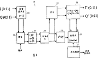
Refer now to Fig. 2,, get illustrated form according to predistortion module 12 of the present invention.Module 12 comprises equalization filter 20, is used to receive the above-mentioned signal of being made up of homophase and quadrature component.Equalization filter is an assembly well known in the art, and it is connected effectively with amplitude limit module 22, and the amplitude limit module in predetermined threshold value, produces limitation signal to signal limitations.The output of amplitude limit module 22 is fed to a low pass filter blocks 24, and the latter eliminates the high fdrequency component that produces because of amplitude limit.
Produce the low pass filter blocks 24 of filtering signal, its output is connected with decimation blocks 26.Decimation blocks 26 to the index calculation module provide the rising sampled signal (as, sampling rate is increased to 8X from 2X).According to the homophase and the quadrature component of baseband signal, computation index value.Computing module is connected with look-up table 30, and the look-up table internal memory contains each parameter.According to the index value that calculates, retrieve each parameter.
Pre-distortion parameters A and B in the look-up table 30 derive from one group of polynomial equation, these equations and make the necessary correction of amplifier characteristic linearisation very approaching.Because the complexity of class ab ammplifier characteristic will obtain useful results, will use a pair of polynomial equation to the B parameter, the A parameter then use single polynomial equation with regard to passable (as approximate, can think the amplitude distortion of A parameter correction amplifier, and the phase distortion of B parameter correction).These polynomial equations can be listed as follows:
To A≤A
m, A=C
0+ C
1P+C
2P
2+ C
3P
3
Otherwise A=A
m
To P≤P
b, B=C
4P+C
5P
2+ C
6P
3
To P>P
b, B=(B
B1-B
B2)+C
7P+C
8P
2+ C
9P
3
Here P=(I
2+ Q
2) be instantaneous envelope power, A
mBe for preventing dark driving amplifier, make it to enter saturation condition and the maximum that is added on A P
bBeing the B parameter carries out the transition to the breakover point of another polynomial equation, B from a polynomial equation
B1And B
B2Be respectively that first and second polynomial equations are at P=P
bThe time the B value, last, C
0To C
9Be the coefficient that is subordinated to specific amplifier, and can be with the temperature of amplifier unit, aging or the like the variation.Certainly, should be understood that, under suitable situation, also can be to the A parameter as the B parameter, with two (2) individual equations.
For adapting to the time variation matter of each coefficient, the present invention adopts a kind of adaptation scheme, and wherein, each coefficient value is optimization (or constantly controlled) constantly, to keep ACP minimum or reduction.As shown in Figure 1, the coupler 17 in amplifier 16 outputs to output sampling, simultaneously, is tuned to the receiver 18 that makes ACP reduction or minimized frequency field, produces a voltage that is directly proportional with received power.Can on more than a frequency, sample with a plurality of receivers, perhaps one after the other be tuned to interested each frequency with single receiver to ACP.Then, the voltage that obtains on different frequency is combined into single amount, and its value will be reduced exactly or be minimized.In general, enough with two frequencies, when with two frequencies, the voltage V that obtains
1And V
2Can make up as follows:
V=V
1+V
2+|(V
1-V
2)|
Here | (V
1-V
2) | be (V
1-V
2) absolute value.Replace providing two value sums simply, use absolute value can make V like this
1And V
2Both reduce or minimize.
Thereby make the appropriate algorithm of V ACP reduction or minimized each coefficient value, it is the simplex algorithm of knowing (Simplex algorithm), Nelder and Mead " ASimplex Method For Function Minimization; " explanation is arranged, see ComputerJournal, Vol.7, PP.308-313 (1965), this article is accommodated in this, for your guidance.To illustrate that below this algorithm is implemented with the form of revising.
Now again with reference to figure 2, the simplex algorithm of modification is by processing module 32 operations.Should be understood that processing module 32 can be used various forms, comprises microprocessor, digital signal processor, or the treatment circuit of use FPGA (field programmable gate array) parts.Should be understood that also after the explanation of reading here, the one skilled in the art should be understood that simplex algorithm can be with the appropriate combination of hardware and software, with any suitable method enforcement.Certainly, the parts (being exactly module 32 here) that are used to implement this algorithm should comprise suitable memory span, to store and to keep operation necessary code of this algorithm and data.
When each iteration, from each coefficient value that this algorithm is derived, be used in the equation of above-mentioned A and B, producing a table, use when the next iteration for this algorithm.This algorithm can continuous service, makes coefficient value can follow the tracks of any variation that occurs in time.
By the simplex optimized algorithm of Nelder and Mead development,, functional value is minimized or reduce functional value by mathematical computations.An importance of its operational mode is that if a certain calculating is repeated, then the functional value of Huo Deing is identical.This numerical value that obtains with measuring with operational hardware is different, because noise and fluctuating obviously can make measurement variation.Carry out real-time simplex algorithm when calculating when attempt with operational hardware, this differential meaning is great.
The essence of simplex algorithm is, during each iteration, the one group coefficient relevant with the worst functional value is presented more one group of new replacement of nice function value.Compare with the optimal function value that obtains so far, new value may be better or may be not good, but proceeds down when algorithm, can look to obtaining more and more better functional value.Suppose that in measurement certain noise and the result who rises and falls and cause are to obtain certain good but wrong exceptionally value.If continue after the value that obtains, all worse than this wrong value, so, this algorithm will converge on this wrong value.Therefore, by the conventionally form of this algorithm, when wanting optimized or continuous in check amount to exist under the situation of macrorelief quite, as present situation, this algorithm is inapplicable.
In order to overcome this difficulty, this simplex algorithm form of the modification that combines with the present invention.When each iteration finished, if best in the past value is replaced by a better value, then algorithm was proceeded next iteration.But, if certain iteration does not produce the value of a new the best, then reappraise existing optimum, and replace value in the past with new value.Therefore, recover the misdata that this algorithm can produce from the measurement that rises and falls.Be the point (it may be best point) that will arrive hope, these fluctuatings can cause a large amount of iteration, but can overslaugh not arrive the point of wishing.
In order to make the simplex algorithm can continuous service, and the follower amplifier characteristic also needs do other modification to this algorithm because of variations in temperature, assembly is aging or other interference causes variation.In the conventional implementation method of this algorithm, set up one and withdraw from criterion (this criterion is usually directed to the percentage of functional value between the worst and optimum of this simplex and changes), when satisfying this criterion, this algorithm just stops.When near that wish or best some, this algorithm will reduce the size of this simplex, and when arriving the point of hope, it is very little that this simplex becomes usually.In case this situation occurs, the variation of this algorithm pair amplifier characteristic will no longer include reaction.In enforcement of the present invention, when iteration begins, should avoid the size of this simplex to become and be significantly smaller than certain value, such as certain default minimum value, when it is reduced to less than this value, it is increased to this value again.Choosing of this value should be enough big, make the variation that this algorithm can the follower amplifier characteristic, again can not be too big, so that can not arrive (or best) point of hope.Suitable value is a such value, and it makes each coefficient value on the worst point of simplex, differs from percent 5 to percent 10 approximately with analog value on optimum.
Continuation is with reference to figure 2, and look-up table 30 is received from from processing module 32 and adapts to feedback.The output of decimation blocks 26 also is connected to delay circuit 34, and the latter then is connected to output module 36, and output module 36 produces output signal effectively according to parameter and rising sampled signal from the look-up table retrieval.
A draw example of the field programmable gate array 800 that is selected from Fig. 2 part of Fig. 8.The data path of I and Q is independently square shown in 802,804, so that produce I
2And Q
2These two values are added up 806, constitute the index address of look-up table 30, and look-up table 30 adopts the two-port RAM memory block 808 of two separation and 810 form, and it comprises A and B parameter respectively.From each parameter of memory block output, the I and the Q value of being delayed time on 812,814,816 and 818 multiply each other, and produce four value: I * A, I * B, Q * A and Q * B.These values are with adders and subtractor block 820 and 822 combinations, constitute (IA-QB) and (QA+IB).The output of these two values provides I ' and Q '.
Should be understood that, for example,, in the time of can in " needs ", obtaining A and B parameter, there is no need to dispose look-up table when processing module has sufficiently high processing speed.At this moment, processing module is calculated each suitable coefficient, and A and B parameter are where necessary or calculated subsequently by processing module when needing again, and need not these parameters are stored in the look-up table.
Later with reference to figure 1, the receiver 18 in the digital predistortion adaptation loop is used to measure the RF power in the arrowband on the characteristic frequency.The frequency that this is tuning, by from for example main CDMA carrier frequency shift, and be offset to will be by on the minimized ACP frequency of optimized algorithm.
Single channel, a single receiver 18 of changing are drawn in Fig. 3.Say that more specifically receiver 18 comprises a frequency synthesizer 50 that is connected with frequency mixer 52.The output of frequency mixer 52 is connected with low pass filter 54, and the latter then is connected to intermediate frequency (IF) loop 56.The output in loop 56 is connected with analog to digital converter 58, and then, analog to digital converter 58 provides input to processing module 32 shown in Figure 2.
Three important frequencies on this block diagram are: radio frequency (RF), and it is the frequency of the adjacent power level that will measure; Local oscillator frequency (LO), it changes with the need, carries out tuning to receiver; Be intermediate frequency (IF) at last, it is fixed.The LO frequency that needs is obtained by LO=RF-IF.
Say that more specifically the RF of receiver 18 input is that the output from power amplifier 16 is coupled out.Broadband RF signal downconverts to intermediate frequency (IF), wherein IF=RF-LO with frequency mixer 52.The LO of frequency mixer is that phase-locked loop (PLL) frequency synthesizer 50 produces.This LO frequency is set with (numeral) tune command of microprocessor.
With the frequency content of low pass filter 54 elimination RF+LO and the feedthrough of RF and LO, and the higher frequency composition of frequency mixer 52 generations.The IF loop 56 of receiver, in Fig. 3 with single box indicating.In certain form, IF loop 56 actual a plurality of amplifiers and narrow band pass filters of comprising, the latter guarantees that the power that will measure is real power on tuned frequency, and does not comprise from, the power of for example main CDMA carrier wave.IF loop 56 also produces a received signal intensity indication (RSSI) output.This voltage is proportional to IF power, and the latter is proportional to RF power again, uses an analog to digital converter (ADC) that this voltage is sampled then.The output of ADC is a numeric word (it represents the power level on the tuned frequency), uses for optimized algorithm.
In some was implemented, optimized algorithm was monitored ACP on a plurality of Frequency points, so single channel receiver must constantly retune.This retunes can be with finishing with following similar step:
-microprocessor (as processing module 32) is sent tune command to frequency and is closed
Grow up to be a useful person.This step will be set LO frequency (thereby tuned frequency of receiver).
-microprocessor is waited for the adjustment of PLL and RSSI.
-microprocessor reads digitized RSSI value.If require average
RSSI then reads a plurality of readings.
-next frequency is repeated these steps.
With reference to Fig. 4, when operation, obtain baseband signal (step 402) according to system of the present invention.By equalization filter, this filter has the characteristic of CDMA standard I S-95 defined, and is well known in the art earlier for these two I and Q baseband signal.
Then, signal is limited (step 404) and filtering (step 406).The example of baseband signal (is example with 1 component) T1, T2 and T3 is drawn on Fig. 5 by time domain, and wherein T1 is the signal before the amplitude limit, and T2 is behind the amplitude limit but the signal before filtering, and T3 is the signal after the low-pass filtering.The example of frequency domain base band CDMA signal F1 is drawn in Fig. 6.The limitation signal F2 and the filtering signal F3 of frequency domain also are drawn on Fig. 6.
The baseband signal of drawing is limited and filtering before rise sampling and predistortion.Along with the increase of power level, Amplifier Gain diminishes, and in other words, amplifier is compressed signal when high power levels.Proofread and correct this compression, be necessary for predistorter signal extension, that is, and at high (I
2+ Q
2) level of increase signal when being worth.Therefore, the peak power of signal is increased by predistorter, and further driving amplifier enters its nonlinear high power of height district.For alleviating this effect, before signal predistortion, the ratio of reduction signal peak power and average power is helpful, when this can surpass certain threshold value at the peak value of signal, realizes by the peak value of restricting signal.The ACP that the amplitude limit operation produces removes with filter, as shown in Figure 6.
Then, to the sampling of rising of amplitude limit and filtering signal, increase to 8X speed (step 408) from original 2X speed.The sampling of rising is necessary because predistortion is a kind of nonlinear operation, it because produce the outer component of channel (with equating of producing of amplifier and opposite) thus must increase the Nyquist frequency, signal band is widened.
Rise after the sampling, calculate (I as the look-up table index
2+ Q
2) value, obtain index value or instantaneous envelope power (step 410).Then, utilize the index value that calculates,, and,, produce the baseband signal I ' and the Q ' (step 414) of output according to of the I and Q sampling the carrying out computing of top equation to time-delay with parameter A and B from look-up table 30 retrievals or acquisition parameter A and B (step 412).Time-delay piece 34 (Fig. 2) is to because of calculating (I
2+ Q
2) and compensate from table search A and B institute time-consuming, make the sampling of I and Q and A and B synchronously arrive IOB 36.
This output signal is output subsequently, and is received machine 18 sampling (step 416).Then, utilize processing module 32 to carry out the receiver 18 of the simplex algorithm of revising, the self adaptation feedback is delivered to look-up table 30.Distortion parameter changes with adaptive mode thus, for system provides best ACP reduction.
A representational CDMA frequency spectrum 700 is drawn in Fig. 7.As shown in the figure, produce exemplary frequency spectrum and increased district Rl and R2 again.In addition, also draw two narrow band frequency N1 and N2 can measure or sample thereon with 18 couples of ACP of receiver.On the curve, this actual bandwidth of 2 is not necessarily drawn in proportion.
According to so far explanation, method of the present invention, its objective is the amplitude by making baseband signal and the predistortion (amplitude is mainly finished by the A parameter, and phase place is mainly finished by the B parameter) of phase place, the non-linear correction that maximum possible is provided of pair amplifier.But, there are some application, wherein the characteristic of signal (as in single channel TDMA (time division multiple access connection) system, the ratio of peak power and average power approaches 1) does not allow amplitude to do big expansion, causes the impossible abundant correction as wishing of amplitude non-linearity of amplifier.In this class is used, can come part to proofread and correct amplitude by abundant phase calibration (by the B parameter) and the suitable Am of setting value, obtain basic improvement.
Top explanation only discloses specific embodiment of the present invention, and purpose is limited the present invention.So the present invention not only is limited in the above embodiments.More precisely, will be appreciated that the one skilled in the art can plan additional embodiments in covering scope of the present invention.
Claims (20)
1. one kind is used to make communication component baseband signal that produce, that have in-phase component and quadrature component, and with the equipment of adaptive mode predistortion, this equipment comprises:
One amplitude limit module, it produces limitation signal effectively the baseband signal amplitude limit;
One filtration module, it eliminates the high fdrequency component of limitation signal effectively to limitation signal filtering, and produces filtering signal;
One decimation blocks, it increases the sampling rate of filtering signal, obtains the signal that rises and sample;
One index calculation module, it is according to the in-phase component and the quadrature component of baseband signal, computation index value effectively;
The look-up table of one storage inside parameter is retrieved these parameters according to index value;
One output module, it produces output signal effectively according to the parameter and the rising sampled signal of look-up table retrieval;
One receiver, it retrieves the sampling of the RF signal that produces according to output signal effectively; With
One processor, it is sampled according to these, provides the self adaptation feedback to look-up table effectively.
2. according to the equipment of claim 1, rising decimation blocks wherein makes sampling rate increase to original four times.
3. according to the equipment of claim 1, index value wherein is to calculate with the summed square of in-phase component and quadrature component.
4. according to the equipment of claim 1, index value wherein is the instantaneous power envelope of baseband signal.
5. according to the equipment of claim 1, parameter wherein is to derive from the polynomial equation that has coefficient.
6. according to the equipment of claim 5, parameter wherein is defined as A and B, and polynomial equation is as follows:
To A≤A
m, A=C
0+ C
1P+C
2P
2+ C
3P
3
Otherwise A=A
m
To P≤P
b, B=C
4P+C
5P
2+ C
6P
3
To P>P
b, B=(B
B1-B
B2)+C
7P+C
8P
2+ C
9P
3
Here P=(I
2+ Q
2) be instantaneous envelope power, A
mBe for preventing dark driving amplifier, make it to enter saturation condition and the maximum that is added on A P
bBeing the B parameter carries out the transition to the breakover point of another polynomial equation, B from a polynomial equation
B1And B
B2Be respectively that first and second polynomial equations are at P=P
bThe time the B value, last, C
0To C
9It is coefficient.
7. according to the equipment of claim 5, self adaptation feedback wherein makes the coefficient optimization.
8. according to the equipment of claim 1, also comprise a time delay module, between decimation blocks and output module.
9. one kind is used to make the baseband signal with in-phase component and quadrature component, and with the method for adaptive mode predistortion, this method comprises:
Produce baseband signal with communication component;
The baseband signal amplitude limit, produce limitation signal;
To limitation signal filtering, eliminate the high fdrequency component of limitation signal, produce filtering signal;
Increase the sampling rate of filtering signal, obtain the signal that rises and sample;
Obtain pre-distortion parameters;
Output is based on the output signal of pre-distortion parameters and rising sampled signal;
The RF signal that produces according to output signal is sampled; With
Provide the self adaptation feedback according to sampling.
10. according to the method for claim 9, wherein increase the sampling rate step, comprise make sampling rate increase to original doubly.
11. according to the method for claim 9, wherein obtain the parameter step, comprise with the summed square of in-phase component and quadrature component and come the computation index value.
12. according to the method for claim 11, acquisition step wherein also comprises from the look-up table search argument.
13., also comprise from the multinomial that has coefficient deriving each parameter according to the method for claim 9.
14. according to the method for claim 13, parameter wherein is to be A and B by defined parameters, the following multinomial of union is derived:
To A≤A
m, A=C
0+ C
1P+C
2P
2+ C
3P
3
Otherwise A=A
m
To P≤P
b, B=C
4P+C
5P
2+ C
6P
3
To P>P
b, B=(B
B1-B
B2)+C
7P+C
8P
2+ C
9P
3
Here P=(I
2+ Q
2) be instantaneous envelope power, A
mBe for preventing dark driving amplifier, make it to enter saturation condition and the maximum that is added on A P
bBeing the B parameter carries out the transition to the breakover point of another polynomial equation, B from a polynomial equation
B1And B
B2Be respectively that first and second polynomial equations are at P=P
bThe time the B value, last, C
0To C
9It is coefficient.
15., also comprise the time-delay of rising sampled signal is inputed to output module according to the method for claim 9.
16. one kind is used to make the baseband signal with in-phase component and quadrature component, with the system of adaptive mode predistortion, this system comprises:
Produce the device of baseband signal with communication component;
The baseband signal amplitude limit, produce the device of limitation signal;
To limitation signal filtering, eliminate the high fdrequency component of limitation signal, produce the device of filtering signal;
Increase the sampling rate of filtering signal, obtain the device of the signal of rising sampling;
Device according to in-phase component and quadrature component computation index value;
According to index value, retrieve the device of each parameter from look-up table;
Output is based on the device of the output signal of the parameter of look-up table retrieval and rising sampled signal;
To the device of sampling according to the RF signal of output signal generation; With
According to sampling, provide the device of self adaptation feedback to look-up table.
17. an equipment that makes baseband signal by the adaptive mode predistortion, this equipment comprises:
One decimation blocks, it increases the sampling rate of filtering signal, obtains the signal that rises and sample;
One calculates the module of pre-distortion parameters effectively;
One output module, it produces output signal effectively according to pre-distortion parameters and rising sampled signal;
One receiver, it retrieves the sampling of the RF signal that produces according to output signal effectively; With
One processor, it is sampled according to these, and the self adaptation feedback is provided effectively.
18. according to the equipment of claim 17, also comprise an amplitude limit module, it is effectively to the baseband signal amplitude limit.
19. according to the equipment of claim 18, also comprise filter module, it carries out filtering to the baseband signal behind the amplitude limit effectively.
20. according to the equipment of claim 17, parameter wherein is to derive from the multinomial that has coefficient.
Applications Claiming Priority (2)
| Application Number | Priority Date | Filing Date | Title |
|---|---|---|---|
| US09/395,490 US7409007B1 (en) | 1999-09-14 | 1999-09-14 | Method and apparatus for reducing adjacent channel power in wireless communication systems |
| US09/395,490 | 1999-09-14 |
Publications (1)
| Publication Number | Publication Date |
|---|---|
| CN1288341A true CN1288341A (en) | 2001-03-21 |
Family
ID=23563261
Family Applications (1)
| Application Number | Title | Priority Date | Filing Date |
|---|---|---|---|
| CN00126391A Pending CN1288341A (en) | 1999-09-14 | 2000-09-12 | Method and device for reducing adjacent channel power in radio communication system |
Country Status (9)
| Country | Link |
|---|---|
| US (1) | US7409007B1 (en) |
| EP (1) | EP1085668B1 (en) |
| JP (1) | JP4676052B2 (en) |
| KR (1) | KR100739356B1 (en) |
| CN (1) | CN1288341A (en) |
| AU (1) | AU773197B2 (en) |
| BR (1) | BR0004033A (en) |
| CA (1) | CA2317901C (en) |
| DE (1) | DE60044485D1 (en) |
Cited By (11)
| Publication number | Priority date | Publication date | Assignee | Title |
|---|---|---|---|---|
| CN100566312C (en) * | 2003-06-27 | 2009-12-02 | 安德鲁有限责任公司 | Be used for the digital pre-distortion that linearisation has the power amplifier of asymmetrical characteristic |
| CN101005323B (en) * | 2001-06-01 | 2010-09-22 | 利兰·斯坦福青年大学托管委员会 | Dynamic digital communication system control |
| CN102265521A (en) * | 2008-12-23 | 2011-11-30 | 北方电讯网络有限公司 | Reducing power levels associated with two or more signals using peak reduction distortion that is derived from a combined signal |
| US8548403B2 (en) | 2007-12-07 | 2013-10-01 | Dali Systems Co., Ltd. | Baseband-derived RF digital predistortion |
| US8811917B2 (en) | 2002-05-01 | 2014-08-19 | Dali Systems Co. Ltd. | Digital hybrid mode power amplifier system |
| US8855234B2 (en) | 2006-12-26 | 2014-10-07 | Dali Systems Co. Ltd. | Method and system for baseband predistortion linearization in multi-channel wideband communications systems |
| US9026067B2 (en) | 2007-04-23 | 2015-05-05 | Dali Systems Co. Ltd. | Remotely reconfigurable power amplifier system and method |
| CN111316708A (en) * | 2017-09-11 | 2020-06-19 | 瑞典爱立信有限公司 | Transmit power control in a wireless communication network |
| CN112262369A (en) * | 2018-07-26 | 2021-01-22 | 上海诺基亚贝尔股份有限公司 | Method, apparatus and computer readable medium for data processing |
| US11159129B2 (en) | 2002-05-01 | 2021-10-26 | Dali Wireless, Inc. | Power amplifier time-delay invariant predistortion methods and apparatus |
| US20220295487A1 (en) | 2010-09-14 | 2022-09-15 | Dali Wireless, Inc. | Remotely reconfigurable distributed antenna system and methods |
Families Citing this family (18)
| Publication number | Priority date | Publication date | Assignee | Title |
|---|---|---|---|---|
| WO2003001664A1 (en) * | 2001-06-25 | 2003-01-03 | Nokia Corporation | Data transmission method and arrangement |
| KR20030024241A (en) * | 2001-09-17 | 2003-03-26 | 엘지전자 주식회사 | Transmission circuit for bluetooth |
| US7248642B1 (en) | 2002-02-05 | 2007-07-24 | Andrew Corporation | Frequency-dependent phase pre-distortion for reducing spurious emissions in communication networks |
| US7197085B1 (en) * | 2002-03-08 | 2007-03-27 | Andrew Corporation | Frequency-dependent magnitude pre-distortion for reducing spurious emissions in communication networks |
| US7266159B2 (en) * | 2002-03-08 | 2007-09-04 | Andrew Corporation | Frequency-dependent magnitude pre-distortion on non-baseband input signals for reducing spurious emissions in communication networks |
| JP3637323B2 (en) | 2002-03-19 | 2005-04-13 | 株式会社東芝 | Reception device, transmission / reception device, and reception method |
| US7139327B2 (en) | 2002-06-10 | 2006-11-21 | Andrew Corporation | Digital pre-distortion of input signals for reducing spurious emissions in communication networks |
| US7450636B2 (en) * | 2002-09-05 | 2008-11-11 | Avago Technologies General Ip (Singapore) Pte. Ltd. | Adaptive transmit equalizer |
| US7035601B2 (en) | 2003-02-27 | 2006-04-25 | Nokia Corporation | Data transmission method, base station and transmitter for compensating for non-linearities in a transmission chain |
| US7738544B2 (en) | 2004-01-30 | 2010-06-15 | Electronics & Telecommunications Research Institute | Apparatus and method for measuring received signal strength indicator, and recording medium storing program embodying the same method |
| KR100553434B1 (en) | 2004-08-13 | 2006-02-20 | 주식회사 팬택앤큐리텔 | Apparatus for receiving rf signal |
| US7787562B2 (en) | 2004-12-29 | 2010-08-31 | Motorola, Inc. | Method and apparatus for adaptive modulation of wireless communication signals |
| JP5085896B2 (en) * | 2006-02-17 | 2012-11-28 | 富士通株式会社 | Signal peak voltage suppressor |
| KR101145830B1 (en) * | 2008-10-29 | 2012-05-17 | 주식회사 케이제이티 | Power output unit with an interference suppress system filter unit and pre-distorter for mobile telecommunication equipments |
| JP5244698B2 (en) * | 2009-05-18 | 2013-07-24 | アイコム株式会社 | Transmission power control apparatus and transmission power control method |
| US8711976B2 (en) | 2011-05-12 | 2014-04-29 | Andrew Llc | Pre-distortion architecture for compensating non-linear effects |
| US8792572B1 (en) * | 2013-05-30 | 2014-07-29 | Telefonaktiebolaget L M Ericsson (Publ) | Universal peak power reduction in communication radios |
| JP2015142325A (en) | 2014-01-30 | 2015-08-03 | 富士通株式会社 | Distortion compensation device and distortion compensation method |
Family Cites Families (14)
| Publication number | Priority date | Publication date | Assignee | Title |
|---|---|---|---|---|
| GB2265270B (en) * | 1992-03-02 | 1996-06-12 | Motorola Ltd | Rf power amplifier with linearization |
| JP2718398B2 (en) * | 1995-06-30 | 1998-02-25 | 日本電気株式会社 | CDMA base station transmitter |
| EP0881807B1 (en) | 1996-11-19 | 2004-04-14 | Matsushita Electric Industrial Co., Ltd | Tansmitter with linearised amplifier |
| JP3221335B2 (en) * | 1996-11-19 | 2001-10-22 | 松下電器産業株式会社 | Nonlinear distortion compensator |
| JP3139395B2 (en) * | 1996-11-19 | 2001-02-26 | 松下電器産業株式会社 | Transmission device |
| US5920808A (en) * | 1996-12-12 | 1999-07-06 | Glenayre Electronics, Inc. | Method and apparatus for reducing key-up distortion by pre-heating transistors |
| US5923712A (en) * | 1997-05-05 | 1999-07-13 | Glenayre Electronics, Inc. | Method and apparatus for linear transmission by direct inverse modeling |
| US5867065A (en) | 1997-05-07 | 1999-02-02 | Glenayre Electronics, Inc. | Frequency selective predistortion in a linear transmitter |
| US5963549A (en) * | 1997-12-10 | 1999-10-05 | L-3 Communications Corporation | Fixed wireless loop system having baseband combiner predistortion summing table |
| US6075411A (en) | 1997-12-22 | 2000-06-13 | Telefonaktiebolaget Lm Ericsson | Method and apparatus for wideband predistortion linearization |
| US6288610B1 (en) * | 1998-03-19 | 2001-09-11 | Fujitsu Limited | Method and apparatus for correcting signals, apparatus for compensating for distortion, apparatus for preparing distortion compensating data, and transmitter |
| US6493543B1 (en) * | 1998-10-19 | 2002-12-10 | Powerwave Technologies, Inc. | Multichannel amplification system using mask detection |
| US6614854B1 (en) * | 1999-05-28 | 2003-09-02 | Carriercomm, Inc. | System and method for adaptive predistortion |
| US6507732B1 (en) | 1999-09-14 | 2003-01-14 | Lucent Technologies Inc. | Dynamic path gain compensation for radios in wireless communication systems |
-
1999
- 1999-09-14 US US09/395,490 patent/US7409007B1/en not_active Expired - Fee Related
-
2000
- 2000-09-04 EP EP00307643A patent/EP1085668B1/en not_active Expired - Lifetime
- 2000-09-04 DE DE60044485T patent/DE60044485D1/en not_active Expired - Lifetime
- 2000-09-06 BR BR0004033-9A patent/BR0004033A/en not_active Application Discontinuation
- 2000-09-07 CA CA2317901A patent/CA2317901C/en not_active Expired - Fee Related
- 2000-09-07 AU AU56554/00A patent/AU773197B2/en not_active Ceased
- 2000-09-12 CN CN00126391A patent/CN1288341A/en active Pending
- 2000-09-13 JP JP2000277712A patent/JP4676052B2/en not_active Expired - Fee Related
- 2000-09-14 KR KR1020000054035A patent/KR100739356B1/en not_active IP Right Cessation
Cited By (18)
| Publication number | Priority date | Publication date | Assignee | Title |
|---|---|---|---|---|
| CN101005323B (en) * | 2001-06-01 | 2010-09-22 | 利兰·斯坦福青年大学托管委员会 | Dynamic digital communication system control |
| US8811917B2 (en) | 2002-05-01 | 2014-08-19 | Dali Systems Co. Ltd. | Digital hybrid mode power amplifier system |
| US11418155B2 (en) | 2002-05-01 | 2022-08-16 | Dali Wireless, Inc. | Digital hybrid mode power amplifier system |
| US11159129B2 (en) | 2002-05-01 | 2021-10-26 | Dali Wireless, Inc. | Power amplifier time-delay invariant predistortion methods and apparatus |
| CN100566312C (en) * | 2003-06-27 | 2009-12-02 | 安德鲁有限责任公司 | Be used for the digital pre-distortion that linearisation has the power amplifier of asymmetrical characteristic |
| US11129076B2 (en) | 2006-12-26 | 2021-09-21 | Dali Wireless, Inc. | Method and system for baseband predistortion linearization in multi-channel wideband communication systems |
| US8855234B2 (en) | 2006-12-26 | 2014-10-07 | Dali Systems Co. Ltd. | Method and system for baseband predistortion linearization in multi-channel wideband communications systems |
| US9246731B2 (en) | 2006-12-26 | 2016-01-26 | Dali Systems Co. Ltd. | Method and system for baseband predistortion linearization in multi-channel wideband communication systems |
| US9026067B2 (en) | 2007-04-23 | 2015-05-05 | Dali Systems Co. Ltd. | Remotely reconfigurable power amplifier system and method |
| US8548403B2 (en) | 2007-12-07 | 2013-10-01 | Dali Systems Co., Ltd. | Baseband-derived RF digital predistortion |
| US9768739B2 (en) | 2008-03-31 | 2017-09-19 | Dali Systems Co. Ltd. | Digital hybrid mode power amplifier system |
| CN102265521B (en) * | 2008-12-23 | 2014-05-07 | 苹果公司 | Method for reducing power levels using peak reduction distortion and transceiver device |
| CN102265521A (en) * | 2008-12-23 | 2011-11-30 | 北方电讯网络有限公司 | Reducing power levels associated with two or more signals using peak reduction distortion that is derived from a combined signal |
| US20220295487A1 (en) | 2010-09-14 | 2022-09-15 | Dali Wireless, Inc. | Remotely reconfigurable distributed antenna system and methods |
| US11805504B2 (en) | 2010-09-14 | 2023-10-31 | Dali Wireless, Inc. | Remotely reconfigurable distributed antenna system and methods |
| CN111316708A (en) * | 2017-09-11 | 2020-06-19 | 瑞典爱立信有限公司 | Transmit power control in a wireless communication network |
| CN112262369A (en) * | 2018-07-26 | 2021-01-22 | 上海诺基亚贝尔股份有限公司 | Method, apparatus and computer readable medium for data processing |
| CN112262369B (en) * | 2018-07-26 | 2024-04-02 | 上海诺基亚贝尔股份有限公司 | Method, apparatus and computer readable medium for data processing |
Also Published As
| Publication number | Publication date |
|---|---|
| EP1085668A3 (en) | 2003-09-03 |
| KR100739356B1 (en) | 2007-07-18 |
| AU5655400A (en) | 2001-03-15 |
| JP4676052B2 (en) | 2011-04-27 |
| KR20010050450A (en) | 2001-06-15 |
| DE60044485D1 (en) | 2010-07-15 |
| CA2317901C (en) | 2011-04-19 |
| CA2317901A1 (en) | 2001-03-14 |
| US7409007B1 (en) | 2008-08-05 |
| EP1085668B1 (en) | 2010-06-02 |
| BR0004033A (en) | 2001-04-17 |
| AU773197B2 (en) | 2004-05-20 |
| EP1085668A2 (en) | 2001-03-21 |
| JP2001127819A (en) | 2001-05-11 |
Similar Documents
| Publication | Publication Date | Title |
|---|---|---|
| CN1288341A (en) | Method and device for reducing adjacent channel power in radio communication system | |
| CN1166138C (en) | Adaptive digital pre-distortion method and device for wideband transmitter | |
| CN1218474C (en) | Power modulation systems and methods that separately amplify low and high frequency portions of an amplitude waveform | |
| CN1578284A (en) | Digital pre-distortion for the linearization of power amplifiers with asymmetrical characteristics | |
| US8982995B1 (en) | Communication device and method of multipath compensation for digital predistortion linearization | |
| RU2563586C2 (en) | Method and apparatus for performing digital baseband prediction | |
| CN1957526A (en) | Amplifier linearization using non-linear predistortion | |
| CN1640086A (en) | Frequency-dependent magnitude pre-distortion for reducing spurious emissions in communication networks | |
| US20080095264A1 (en) | Device and method for pre-distorting a base-band digital signal | |
| US9054940B2 (en) | System and method for linearizing power amplifiers | |
| CN1448011A (en) | System and method for peak power reduction in multiple carrier communications systems | |
| CN1701521A (en) | Transmission device and adjustment method thereof | |
| CN101188433A (en) | Method and system for AM in wireless communication system | |
| CN1781298A (en) | Compensating for analog radio component impairments to relax specifications | |
| CN101355536B (en) | Apparatus and method for implementing predistortion treatment of baseband signal | |
| CN1747460A (en) | Delay locked loop circuit, digital predistortion type transmitter using same, and wireless base station | |
| CN1531213A (en) | Signal sampler acquring technology | |
| CN104954294A (en) | Transmitter branch phase mismatch detection and correction system | |
| US9337783B2 (en) | Distortion compensation apparatus and distortion compensation method | |
| US6903619B2 (en) | Electromagnetic wave transmitter systems, methods and articles of manufacture | |
| CN1666408A (en) | Predistortion control | |
| US8224265B1 (en) | Method for optimizing AM/AM and AM/PM predistortion in a mobile terminal | |
| CN102904846B (en) | A kind of digital pre-distortion processing method adapting to fast changed signal | |
| US20040264596A1 (en) | Digital pre-distortion for the linearization of power amplifiers with asymmetrical characteristics | |
| CN1643782A (en) | An implementation method for pre-distortion of non-linear devices |
Legal Events
| Date | Code | Title | Description |
|---|---|---|---|
| C06 | Publication | ||
| PB01 | Publication | ||
| C10 | Entry into substantive examination | ||
| SE01 | Entry into force of request for substantive examination | ||
| C02 | Deemed withdrawal of patent application after publication (patent law 2001) | ||
| WD01 | Invention patent application deemed withdrawn after publication |