CN1315138C - Formation of thin-film capacitor - Google Patents
Formation of thin-film capacitor Download PDFInfo
- Publication number
- CN1315138C CN1315138C CNB991244885A CN99124488A CN1315138C CN 1315138 C CN1315138 C CN 1315138C CN B991244885 A CNB991244885 A CN B991244885A CN 99124488 A CN99124488 A CN 99124488A CN 1315138 C CN1315138 C CN 1315138C
- Authority
- CN
- China
- Prior art keywords
- layer
- dielectric materials
- metal
- deposit
- solution
- Prior art date
- Legal status (The legal status is an assumption and is not a legal conclusion. Google has not performed a legal analysis and makes no representation as to the accuracy of the status listed.)
- Expired - Fee Related
Links
Images


Classifications
-
- H—ELECTRICITY
- H05—ELECTRIC TECHNIQUES NOT OTHERWISE PROVIDED FOR
- H05K—PRINTED CIRCUITS; CASINGS OR CONSTRUCTIONAL DETAILS OF ELECTRIC APPARATUS; MANUFACTURE OF ASSEMBLAGES OF ELECTRICAL COMPONENTS
- H05K1/00—Printed circuits
- H05K1/16—Printed circuits incorporating printed electric components, e.g. printed resistor, capacitor, inductor
- H05K1/162—Printed circuits incorporating printed electric components, e.g. printed resistor, capacitor, inductor incorporating printed capacitors
-
- H—ELECTRICITY
- H01—ELECTRIC ELEMENTS
- H01G—CAPACITORS; CAPACITORS, RECTIFIERS, DETECTORS, SWITCHING DEVICES OR LIGHT-SENSITIVE DEVICES, OF THE ELECTROLYTIC TYPE
- H01G4/00—Fixed capacitors; Processes of their manufacture
- H01G4/002—Details
- H01G4/018—Dielectrics
- H01G4/06—Solid dielectrics
- H01G4/08—Inorganic dielectrics
- H01G4/085—Vapour deposited
-
- H—ELECTRICITY
- H01—ELECTRIC ELEMENTS
- H01G—CAPACITORS; CAPACITORS, RECTIFIERS, DETECTORS, SWITCHING DEVICES OR LIGHT-SENSITIVE DEVICES, OF THE ELECTROLYTIC TYPE
- H01G4/00—Fixed capacitors; Processes of their manufacture
- H01G4/002—Details
- H01G4/018—Dielectrics
- H01G4/06—Solid dielectrics
- H01G4/08—Inorganic dielectrics
- H01G4/10—Metal-oxide dielectrics
-
- H—ELECTRICITY
- H05—ELECTRIC TECHNIQUES NOT OTHERWISE PROVIDED FOR
- H05K—PRINTED CIRCUITS; CASINGS OR CONSTRUCTIONAL DETAILS OF ELECTRIC APPARATUS; MANUFACTURE OF ASSEMBLAGES OF ELECTRICAL COMPONENTS
- H05K2201/00—Indexing scheme relating to printed circuits covered by H05K1/00
- H05K2201/01—Dielectrics
- H05K2201/0137—Materials
- H05K2201/0175—Inorganic, non-metallic layer, e.g. resist or dielectric for printed capacitor
-
- H—ELECTRICITY
- H05—ELECTRIC TECHNIQUES NOT OTHERWISE PROVIDED FOR
- H05K—PRINTED CIRCUITS; CASINGS OR CONSTRUCTIONAL DETAILS OF ELECTRIC APPARATUS; MANUFACTURE OF ASSEMBLAGES OF ELECTRICAL COMPONENTS
- H05K2201/00—Indexing scheme relating to printed circuits covered by H05K1/00
- H05K2201/01—Dielectrics
- H05K2201/0137—Materials
- H05K2201/0179—Thin film deposited insulating layer, e.g. inorganic layer for printed capacitor
-
- H—ELECTRICITY
- H05—ELECTRIC TECHNIQUES NOT OTHERWISE PROVIDED FOR
- H05K—PRINTED CIRCUITS; CASINGS OR CONSTRUCTIONAL DETAILS OF ELECTRIC APPARATUS; MANUFACTURE OF ASSEMBLAGES OF ELECTRICAL COMPONENTS
- H05K2201/00—Indexing scheme relating to printed circuits covered by H05K1/00
- H05K2201/03—Conductive materials
- H05K2201/0302—Properties and characteristics in general
- H05K2201/0317—Thin film conductor layer; Thin film passive component
-
- H—ELECTRICITY
- H05—ELECTRIC TECHNIQUES NOT OTHERWISE PROVIDED FOR
- H05K—PRINTED CIRCUITS; CASINGS OR CONSTRUCTIONAL DETAILS OF ELECTRIC APPARATUS; MANUFACTURE OF ASSEMBLAGES OF ELECTRICAL COMPONENTS
- H05K2201/00—Indexing scheme relating to printed circuits covered by H05K1/00
- H05K2201/03—Conductive materials
- H05K2201/0332—Structure of the conductor
- H05K2201/0335—Layered conductors or foils
- H05K2201/0355—Metal foils
-
- H—ELECTRICITY
- H05—ELECTRIC TECHNIQUES NOT OTHERWISE PROVIDED FOR
- H05K—PRINTED CIRCUITS; CASINGS OR CONSTRUCTIONAL DETAILS OF ELECTRIC APPARATUS; MANUFACTURE OF ASSEMBLAGES OF ELECTRICAL COMPONENTS
- H05K2201/00—Indexing scheme relating to printed circuits covered by H05K1/00
- H05K2201/09—Shape and layout
- H05K2201/09209—Shape and layout details of conductors
- H05K2201/0929—Conductive planes
- H05K2201/09309—Core having two or more power planes; Capacitive laminate of two power planes
-
- H—ELECTRICITY
- H05—ELECTRIC TECHNIQUES NOT OTHERWISE PROVIDED FOR
- H05K—PRINTED CIRCUITS; CASINGS OR CONSTRUCTIONAL DETAILS OF ELECTRIC APPARATUS; MANUFACTURE OF ASSEMBLAGES OF ELECTRICAL COMPONENTS
- H05K3/00—Apparatus or processes for manufacturing printed circuits
- H05K3/38—Improvement of the adhesion between the insulating substrate and the metal
- H05K3/388—Improvement of the adhesion between the insulating substrate and the metal by the use of a metallic or inorganic thin film adhesion layer
-
- H—ELECTRICITY
- H05—ELECTRIC TECHNIQUES NOT OTHERWISE PROVIDED FOR
- H05K—PRINTED CIRCUITS; CASINGS OR CONSTRUCTIONAL DETAILS OF ELECTRIC APPARATUS; MANUFACTURE OF ASSEMBLAGES OF ELECTRICAL COMPONENTS
- H05K3/00—Apparatus or processes for manufacturing printed circuits
- H05K3/46—Manufacturing multilayer circuits
- H05K3/4644—Manufacturing multilayer circuits by building the multilayer layer by layer, i.e. build-up multilayer circuits
- H05K3/467—Adding a circuit layer by thin film methods
-
- Y—GENERAL TAGGING OF NEW TECHNOLOGICAL DEVELOPMENTS; GENERAL TAGGING OF CROSS-SECTIONAL TECHNOLOGIES SPANNING OVER SEVERAL SECTIONS OF THE IPC; TECHNICAL SUBJECTS COVERED BY FORMER USPC CROSS-REFERENCE ART COLLECTIONS [XRACs] AND DIGESTS
- Y02—TECHNOLOGIES OR APPLICATIONS FOR MITIGATION OR ADAPTATION AGAINST CLIMATE CHANGE
- Y02P—CLIMATE CHANGE MITIGATION TECHNOLOGIES IN THE PRODUCTION OR PROCESSING OF GOODS
- Y02P70/00—Climate change mitigation technologies in the production process for final industrial or consumer products
- Y02P70/50—Manufacturing or production processes characterised by the final manufactured product
Abstract
Thin layer capacitors are formed from a first flexible metal layer, a dielectric layer between about 0.03 and about 2 microns deposited thereon, and a second flexible metal layer deposited on the dielectric layer. The first flexible metal layer may either be a metal foil, such as a copper, aluminum, or nickel foil, or a metal layer deposited on a polymeric support sheet. Depositions of the layers is by or is facilitate by combustion chemical vapor deposition or controlled atmosphere chemical vapor deposition.
Description
Technical field
The present invention relates to film capacitor, be preferred for the formation of the film capacitor of printed circuit, this film capacitor can be embedded in the printed circuit board (PCB).Especially, the present invention relates to by preparing film capacitor by the thin layer of dielectric material of combustion chemistry vapour deposition deposit.
Background technology
Combustion chemistry vapour deposition (" CCVD "), a kind of newly-invented CVD technology, can be in opening wide atmosphere deposition film.CCVD method and other thin film technique comprise that conventional CVD compares and has many advantages.The major advantage of CCVD is a deposition film in the atmosphere of opening wide, and need not any sealed furnace, vacuum or reative cell.Therefore, compare with the system based on vacuum, the required initial investment of this system is the highest to reduce by 90%.The specific environment that is different from other Technology Need, combustion flame provide from the required environment of the elemental constituent deposit of solution, steam or gas source.This precursor is dissolved in the solvent that can be used as the fuel use simultaneously usually.Deposit also can be under atmospheric pressure with ambient temperature under at hood, outdoor or in the chamber of control ambient gas and pressure, carry out.
Because CCVD generally uses solution, so the significant advantage of this technology is that it can be fast and changes dopant and stoichiometry simply, is easier to the film of deposit complexity.The CCVD technology is used cheap, soluble precursor usually.In addition, as a rule, the vapour pressure of precursor does not play a major role in CCVD, because course of dissolution is provided for producing the energy of desired ion component.By regulator solution concentration and component, can be fast and deposit easily very on a large scale in stoichiometric composition.Therefore, the CCVD method can make the chemical composition of deposited film and physical structure these two satisfies the requirement of application-specific.
Be different from conventional CVD, that the CCVD method needn't be limited to is expensive, fixing, in the low pressure reaction chamber.Therefore, deposit flame or flame bundle can move and cross substrate so that apply big and/or the complex surfaces zone.Because the CCVD method is not subjected to the restriction of specific environment, so the user can add raw material continuously in coating zone, need not to interrupt, therefore also may be carried out batchwise.In addition, the user can be limited in these zones with deposit by controlling the time of staying of flame on the substrate specific region simply.At last, the CCVD technology uses the obviously reduction of halogen to the precursor of environment adverse effect usually.
Through CCVD technology and can the various material of deposit as the burning of the premixed precursor of unique thermal source.The deposition technology of this cheapness and flexible membrane can be widened the range of application of thin film technique.The CCVD method has the pliability roughly the same with thermal spraying, and produces film high-quality, conformal, and the film relevant with conventional CVD is the same.By means of the CCVD method, can be in several days, with the low relatively desirable phase of cost deposit.
CCVD method embodiment preferred is described in detail in the U. S. application number 08/691,853 of on August 2nd, 1996 application, and this technology is incorporated herein for your guidance.According to this application, the CCVD method is to prepare film, powder and the nanoscale coating that steam forms by nearly supercritical liq and supercritical liq.Preferably, form high-quality and contain the liquid of precursor or the fluid of class I liquid I solution.This solution fluid adjusted to be close to or higher than critical pressure, then, just before discharging, be heated to, wherein produce a kind of gas of carrying the solution fluid of very thin atomizing or evaporation secretly by air throttle or nozzle near supercritical temperature by air throttle or nozzle.This solution fluid steam burning forms flame or enters flame or the electron gun plasma, and precursors reaction is desirable phase in flame or plasma or on substrate surface.Because the temperature of plasma height, most precursors will be in the reaction of the front of substrate surface.Substrate be placed near flame or the electro-plasma or among, and deposit coating.Perhaps, formed material is collected as nanometer grade powder.
Very thin atomizing, spraying, evaporation or gasification can be adopted and be close to or higher than critical pressure and obtain near the solution fluid of critical temperature.The precursor of dissolving need not high evaporating pressure, but the precursor of high evaporation pressure can be fine or be worked better than low evaporating pressure precursor, by just before the end of nozzle or air throttle pipe (atomising device) or at its end heated solution fluid, precursor before atomizing chemical reaction or be reduced to minimum the effective time of decomposition. this method can be used for by various metallorganics and inorganic precursor deposit coating.The fluid solution solvent is selected from any liquid or the supercritical fluid that can make precursor form solution therein.
The reduction of supercritical temperature that contains the fluid of reactant produces the coating of high-quality.Many such fluids are unsettled as liquid under STP, and must be at pressurized tank or mix at low temperatures.In order more easily to form liquid or the fluid solution that only exists under the pressure of projecting environment, randomly precursor at first dissolves and is in first stable under the atmospheric pressure solvent.This solution is placed in the balancing gate pit, adds second (or main) liquid or fluid (wherein can sneak into first solution) then.This main liquid or fluid have low supercritical temperature, and the required maximum temperature of spraying degree that causes wishing reduces.Owing to form high concentration first solution, the low concentration solution majority that obtains is formed with the solubilize compound that may add by second.Generally, the ratio of given compound is high more in given solution, and the performance of this solution is similar to this compound more so.The solution of selecting these additional liquid and fluid to help to contain precursor atomizes very carefully, evaporates or gasifies.Selection has possibility that the final solution mixture of low supercritical temperature additionally can make precursor react and reduces to minimumly in atomising device, and reduce or eliminate needs at the release areas heated solution.In some cases, before release areas, this solution can be cooled off, the stability of solubility and fluid can be kept like this.The professional in supercritical fluid solution field can determine various possible solution mixtures, and need not undue complicated experiment.Randomly, has windowpane or have optical fiber and the pressure vessel of monitor can allow to estimate the compatibility of Combination and solute one solvent.On the contrary, if pot strainer is blocked or find that sediment remains in the primary tank, so under these conditions incompatibility may appear.
Other advantage is that the release that is close to or higher than the fluid of their super critical points causes rapid expanding, forms the high-speed gas vapor stream.High velocity gas stream is reduced in the gaseous diffusion boundary layer before the deposition surface effectively, and conversely, it has improved film quality and deposition efficiency.When air velocity is higher than flame speed, must use pilot light or other igniter to be in the flame of stable state with formation.In some cases, need two or more pilot lights to guarantee completing combustion.In addition, replace flame, precursor can pass hot gas, plasma, laser or other energy band.When using plasma flare and other energy band, need not pilot light, and just can obtain high speed by the known operating condition of those of ordinary skills.
The fluid that contains solute does not need fuel when burning.Non-flammable fluid such as water, N
2O or CO
2The fluid such as the ammonia that perhaps are difficult to burn are used to dissolve precursor, perhaps can be used as the second solubilize compound and use.Then, they expand to precursor provides in the flame or plasma flare of reaction environment.Deposit can be higher than, be lower than or atmospheric pressure under carry out.Under reduced pressure plasma flare can be worked better.It is stable that flame is low to moderate under 10 torrs at pressure, and can better work under high pressure.Under low pressure, can form even be lower than 500 ℃ cool flame.If these two can be operated under the atmosphere of opening wide, so advantageously under controlled atmospher reative cell implement method of the present invention with the coating of avoiding carrying secretly the impurity in the atmosphere into and being obtained in.Can not there be such impurity in many electricity or the optical coating application requirements coating.These are used needs film usually, but also can the deposit thick film for heat resistant layer, corrosion and wear applications.
By prolonging deposition time, can obtain massive material, comprise monocrystalline.The quick epitaxial diposition speed (because higher diffusion velocity) that provides by higher deposition temperature is essential for single-crystal thick films or massive material.
CCVD is a kind of flame method of using oxygen.Although can be by in the reduction part of flame, using the CCVD deposit to come the oxidable material of deposit, but a kind of technology preferably of deposit oxidizable material is the Application No. 09/067 that is described in application on April 20th, 1998, correlation technique in 975, the instruction in this application is incorporated herein for your guidance.
In Application No. for reference 09/067, this invention of describing in 975 provides a kind of apparatus and method of chemical vapor deposition, wherein the atmosphere in the coating depositing region is by the material that is used to form coating that careful control and isolation added with determine by barrier region by the gas that depositing region is discharged, wherein gas is with greater than 50 feet per minute clocks in barrier region, and the average speed that is preferably greater than 100 feet per minute clocks flows out from described depositing region.The fast gas stream that passes barrier region can not make the gas in the ambient atmosphere enter depositing region basically, because otherwise they will or form the material reaction of coating with coating.Can carefully control the material that is used to form coating by in liquid medium, adding coating precursor with fixing ratio.Be atomized when liquid medium adds conversion zone, and liquid medium is evaporated in this conversion zone, the coating precursor reaction forms the coating precursor of reaction.In addition, coating precursor can be used as gas (perhaps itself or as with the mixture of carrier gas) add.The reaction coating precursor generally includes part, all and small part reactive component, and it can be used as plasma and flows in the depositing region.The reaction coating precursor contacts and is deposited on this surface with the surface of substrate in depositing region.In that can being provided around the conversion zone, an inert gas curtain that flows avoid the material that reaction coating material/plasma in this zone uses in by surrounding devices and the component of ambient atmosphere to pollute.
In the conversion zone, the reaction needed intake of the evaporation of liquid medium and coating precursor.Required energy can mix by for example resistance heating, the inductance heating of various source, microwave heating, RF heating, hot surface heating and/or with hot inert gas to be provided.
Here, non-combustion method will be called as controlled atmospher combustion chemistry vapor deposition CCVD.This technology provides a kind of energy input speed of relative control, has high coating deposition speed.Under some preferred situations, liquid medium and/or second gas that is used for atomising liquid media can be the combustible fuel that CACCVD uses.Particularly importantly CACCVD have can or be higher than under the atmospheric pressure and form high-quality ability of adhering to illuvium, therefore, need not to enter complicated vacuum or similarly in the insulating case.For these reasons, in many cases, the CACCVD film coating can apply on the spot, perhaps applies in the place of placing substrate.
Combustion chemistry vapour deposition CCVD is not suitable for those coatings applications fields that needs oxygen-free environment.Use for these, adopt the non-burning energy for example the CACCVD of hot gas, heating tube, radiant energy, microwave and excitation photons and infrared or lasing light emitter be fit to.In these were used, importantly employed all liq and gas all were anaerobics.Coating precursor can be incorporated in liquid for example in the solution or suspension in ammonia or the propane, wherein ammonia and propane are suitable for deposition of nitride or carbide respectively.
The CACCVD method and apparatus can be controlled the atmosphere in the depositing region, therefore can form sensitive coating on the substrate of responsive to temperature or vacuum sensitivity, and this substrate can be bigger than the substrate that adopts conventional vacuum chamber deposition technology to handle.
Another advantage of CACCVD be need not on substrate, to apply extra energy just can coated substrate.Correspondingly, this system can apply such substrate, and promptly this substrate does not bear the temperature that most of previous systems stand substrate in advance.For example, on the polyamide slices substrate, can form nickel coating, and can not cause substrate distortion.Atmospheric pressure deposition technology in the past can not provide the chemical vapor deposition layer of metallic nickel, because this metallic nickel has strong affinity to oxygen, and because the degassing of water and be in heat and vacuum size of following time is difficult for stablely, the vacuum processing of polyamide slices substrate is debatable.
Summary of the invention
The present invention relates to the method that forms film capacitor especially, and wherein one deck at least of preferred this capacitor is to pass through CCVD or CACCVD deposit aptly.Usually, capacitor comprises the pair of conductive plate and places dielectric material between the conductive plate, so this strip has electric charge.Film capacitor formed according to the present invention comprises the thin layer of the dielectric material that closely contacts with conductive plate layer and form.
The simple structure of a film capacitor is, forms dielectric materials layer on metal forming or metal level, forms second metal level at the reverse side of dielectric materials layer.Such three-decker itself is exactly a capacitor, and can for example use as decoupling capacitor.
Use the three-decker of above describing,, form pattern on second metal level that particularly forms on the dielectric layer and make a plurality of discrete capacitor by forming pattern on one of conductive layer at least.The formation pattern can be by the photetching technology of routine and is undertaken by the etching of metal level subsequently on metal level, forms the pattern that divides riser like this on a surface of dielectric materials layer.In such structure, with respect to the discrete capacitor plate of butt joint, another metal level for example metal foil layer uses as the common-battery container panel of carrying electric charge.Perhaps, these two metal levels all can form pattern by the photetching technology.
Can use equally be deposited on polymer film for example the thin metal layer on the polyamide membrane replace using the ground floor of metal forming as ground floor.Subsequently, the deposit dielectric materials layer and second metal level thereon.Can on second metal level, form pattern according to the method described above, to make the discrete capacitor plate.
Also can on dielectric materials layer, form pattern by photetching/etching technique.For example, the glass based on silicon dioxide that is deposited as dielectric materials layer of the present invention also can use two ammonium hydrogen difluorides, fluoboric acid and their mixture to come etching.
For example at U.S. Patent number 5,079, the structure of capacitor has been described in 069,5,155,655 and 5,410,107, the instruction of these applications is incorporated herein for your guidance.
Consider the reason of dismounting, durability, circulation weight (flow weight) and the thermal expansion etc. of material for having to, be used for bigger area and some pliabilities of film capacitor needs of printed circuit board (PCB).The layer structure that forms capacitor must have some pliabilities.This is different from less harder silicon wafer technology.Because pliability is essential and because the dielectric material used herein nature of glass normally, silicon dioxide for example, so dielectric layer is extremely thin, for example 2 microns or thinner, preferred 1 micron or thinner.
Backing material also can be rolled, and can obtain various width and length.Material for example metal forming and polymer satisfies these requirements, and silicon can not.Because silicon is rigidity, can not outgas and have less size, so the equal deposit silicon at an easy rate of most of technology.CCVD can use the coating of high-quality to apply desirable substrate.
According to the present invention, on the substrate of flexibility, form film capacitor, wherein this capacitor can embed in the printed circuit board (PCB).On flexible substrate, form thin dielectric materials layer.Preferably, by combustion chemistry vapour deposition (CCVD) deposit dielectric material on substrate.
In one embodiment of this invention, in metal forming deposition of dielectric layer on copper, nickel or the aluminium foil for example.Then, at reverse side deposit second conductive layer of dielectric layer, normally metal level.Second conductive layer can come deposit by CCVD or CACCVD fully.Perhaps, the platinum layer that seed crystal (seed) layer is for example thin can come deposit by CCVD, forms thicker metal level by electroplating then, thereby constitutes three layer capacitor structures.Three layer capacitor structures like this can perhaps can further be processed this three-decker without processing as for example decoupling capacitor use of capacitor, form a plurality of capacitor elements.Thin film capacitor structure described herein generally is embedded in dielectric material for example in the epoxy resin-matrix mylar, so just can use as capacitor layer in electronic circuit board.
This class of instruction embeds capacitor and can further make printed circuit board (PCB) (PCBs) miniaturization in the present invention because no longer need when making must be enough greatly so that handle and be convenient to be welded to discrete capacitor on the track on the printed circuit board surface with manipulator or people.
Description of drawings
The schematic diagram of accompanying drawing 1 expression apparatus of the present invention.
The schematic representation of apparatus of nearly overcritical and overcritical atomizing deposited film and powder is used in accompanying drawing 2 expressions.
The detailed schematic diagram of sprayer that accompanying drawing 3 expressions are used in the present invention.
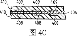
Accompanying drawing 4A, 4B and 4C comprise or the sectional view of the capacitor that formed by the three-decker of metal forming, dielectric layer and deposited metal.
Accompanying drawing 5A and 5B are the sectional views of four layer capacitor structures of polymer film, first deposited metal, dielectric materials layer and second deposited metal composition.
Accompanying drawing 6 is the sectional views that comprise the 5-layer structure of metal forming, barrier layer, dielectric layer, adhesion layer and deposited metal.
Accompanying drawing 7 is the part schematic diagrames that are used for the device of applying coating among the present invention.
Accompanying drawing 8 is the application head part close-up views partly that use in accompanying drawing 7 devices.
Embodiment
The detailed description and the accompanying drawings with reference to the following preferred embodiment of the invention are easier to understand the present invention.
Obvious term used herein only is in order to describe specific embodiment.Be not to be intended to limit the present invention.Should be noted that the singulative that uses " a ", " an " and " the " also comprise plural situation, unless otherwise in specification and appending claims.
In whole application, in order to describe the situation of the prior art relevant with the present invention in more detail, the public publication of quoting is all given references, and the disclosure of these public publications is all introduced for your guidance at this.
The invention provides a kind of method of using selected coated materials substrate.This method comprises, under first temperature of selecting and first pressure of selecting, one or more can be reacted (here, for single precursor, reagent is settled out from solution or chemical bond changes all is considered to a kind of " reaction ") agent dissolves that forms selected material in suitable carriers, form delivered solution.Before really carrying out deposit, sometime, substrate is placed in the zone with second selection pressure.Second selection pressure can be an atmospheric pressure, and usually above 20 torrs.Then, the working pressure adjusting device is forced into delivered solution the 3rd selection pressure that is higher than second selection pressure.This area professional will notice that many suitable pressure-regulating devices are arranged here, comprise compressor etc., but be not limited thereto.Then, the delivered solution of pressurization enters the fluid delivery tube with input and relative output, and temperature-adjusting device is placed on output, is used for the temperature of regulator solution at output.The output of feed tube further comprises and is used for the fluid of feed tube is sent into this zone and the outlet on the substrate direction.The shape of this outlet is similar to nozzle or the choke valve that uses in other injection and atomizing application.Afterwards, the serviceability temperature adjusting device heats this solution to the second and selects temperature, and second selects the critical temperature of temperature than solution, T
c, being more or less than in 50 ℃, the working pressure adjusting device keeps the 3rd selection pressure to be higher than second selection pressure and the respective liquid or the critical pressure that are higher than solution under the second selection temperature, P simultaneously
cThen, exert pressure and outlet that the solution that heats passes feed tube enters this zone, on the direction of substrate, obtain the solution jetting fluid of spraying.When the solution jetting fluid enters this zone, can in the solution jetting fluid of spraying, sneak into one or more and select gas, the jetting fluid that formation can be reacted, afterwards, the jetting fluid that can react is exposed under the energy under the shot point of selecting.But this energy provides enough energy to make reactive spray liquid (it comprises one or more delivered solution reagent) reaction, therefore forms coating material and coated substrate.
In the another embodiment of this method, the energy comprises that the shot point of flame source and selection comprises ignition point.In the other method scheme, the energy comprises plasma flare and heated air.
In the other method scheme of this method, second selection pressure in zone is an ambient pressure.
In yet another embodiment, the solution jetting fluid of atomizing is steam or maximum droplet size less than 2 microns aeroge.
In another embodiment, reduce by second selection pressure in zone, be lower than 1000 ℃ combustion flame to produce temperature.
In yet another embodiment, carrier is a propane, and delivered solution comprises the propane of at least 50 volume %.In another embodiment, delivered solution further comprises butanols, methyl alcohol, isopropyl alcohol, toluene or their mixture.In yet another embodiment, select carrier so that defeated solution under standard temperature and pressure (STP), is being enough to finish essentially no precipitation in the time of this method.
In another alternative embodiment of this method, the working pressure container, and before the step of exerting pressure, during or afterwards, standard temperature and pressure (STP) gas is contacted being enough to form under the selection pressure of liquid or supercritical fluid (depending on temperature) with delivered solution.In preferred embodiments, the delivered solution that contains standard temperature and pressure (STP) gas is being enough to finish essentially no precipitation in the time of this method under the pressure of selecting.In yet another embodiment, the reagent concentration of delivered solution is 0.0005M to 0.05M.
In another embodiment, the output of feed tube further comprises fluid intake, before the flow of solution of pressurization and heating is crossed the feed tube outlet, adds fluid through fluid intake in pressurization, heated solution.Such adding forms a kind of composite solution with supercritical temperature of reduction.
In yet another embodiment, one or more reagent vapour pressure separately is not less than about 25% of carrier vapour pressure.
In yet another embodiment, the output of feed tube comprises that internal diameter is 2 to 1000 microns, preferred 10 to 250 microns conduit.The output of feed tube comprises that internal diameter is 25 to 125 microns a conduit in a preferred embodiment.In another preferred embodiment, the output of feed tube comprises that internal diameter is 50 to 100 microns a conduit.
In yet another embodiment, temperature-adjusting device comprises by applying the device from the current resistor heating feed tube of the selection voltage of current source.In preferred embodiments, voltage is lower than 115 volts.In another embodiment preferred, the device that is used for the resistance heating feed tube is included in the contact of arranging in 4 millimeters of the outlets.
In addition, the present invention also provide a kind of wherein select carrier and one or more reagent to make second to select temperature be the said method of ambient temperature.
Said method can be implemented, and wherein the material of coated substrate comprises the mixture of metal, metal or quasi-metal oxide or metal and metal or quasi-metal oxide.
In yet another embodiment, but reactive spray liquid comprises the flammable jetting fluid with flammable jet velocity, wherein flammable jet velocity greater than the flame speed of flame source, and comprises that further one or more are used to light the ignition-assist apparatus of flammable jetting fluid when ignition point.In preferred embodiments, one or more ignition-assist apparatus comprise a pilot light separately.In another embodiment preferred, be higher than mach one.
In another embodiment, ignition point or flame front remain in 2 centimetres of outlets.
The present invention also provides a kind of method, wherein during exposing step, uses substrate cooling device cooling substrate.In preferred embodiments, the substrate cooling device comprises the device that water is transported to substrate surface.Yet this area professional will recognize also can use many other suitable cooling devices.
In yet another embodiment, the thickness of the material of coated substrate is less than 500 nanometers.In another embodiment, the material of coated substrate comprises the composition of classification.In yet another embodiment, the material of coated substrate comprises amorphous materials.In yet another embodiment, the material of coated substrate comprises nitride, carbide, puff, metal or other oxygen-free material.
The present invention also provides a kind of method, and this method comprises that further the shroud gas of selection flows round reactive jetting fluid, therefore reduces the impurity of carrying secretly and keeps gratifying deposit environment.
In preferred embodiments, second selection pressure is higher than 2.66kPa.
With reference to accompanying drawing 1, preferred equipment 100 comprises, pressure-regulating device 110, pump for example, be used for applying first selection pressure for delivered solution T (being also referred to as " precursor solution ") at delivered solution storage tank 112, wherein delivered solution T comprises suitable carriers, be dissolved with one or more in this carrier and can react the reagent that forms selected material, wherein, under the temperature of carrying liquid T, the device 110 that is used to exert pressure can keep first selection pressure to be higher than the pressure of delivered solution respective liquid (if temperature is lower than T
c) or critical pressure P
cFluid delivery tube 120, it has and the input 122 of delivered solution storage tank fluid connection and relative output 124, this output can make the fluid in the feed tube 120 flow into the second selection pressure zone 130 that is lower than first selection pressure, and on the direction of substrate 140, its middle outlet 126 further comprises the device 128 (referring to accompanying drawing 2 and 3, atomizer 4) that is used to make solution spray formation atomized soln injection stream N; Temperature-adjusting device 150, output 124 hot links of itself and fluid delivery tube 120 arrange, is used for being at output 124 being higher or lower than solution supercritical temperature (T
c) regulator solution temperature in 50 ℃ the scope; Gas supply device 160, it is used for one or more gas (for example oxygen) (not shown) is sneaked into atomized soln spray liquid N, forms reactive spray liquid; The energy 170, it puts 172 places in selective exitation, is used to make the reaction of reactive spray liquid, so this energy 170 provides enough energy that reactive spray liquid is reacted in the zone 130 of second selection pressure, and is coated on the substrate 140.
In the embodiment of another equipment, the energy 170 comprises that flame source and selective exitation point 172 comprise ignition point.In yet another embodiment, the energy 170 comprises plasma flare.In yet another embodiment, outlet 126 further comprises pressure throttling arrangement (referring to accompanying drawing 3, choke valve 7).
In another equipment embodiment, second selection pressure in zone is an atmospheric pressure.
In yet another embodiment, the solution jetting fluid of atomizing is steam or maximum droplet size less than 2 microns aeroge.
In another embodiment, reduce by second selection pressure in zone, be lower than 1000 ℃ combustion flame with the production temperature.
In yet another embodiment, carrier is a propane, and delivered solution comprises the propane of at least 50 volume %.In another embodiment, delivered solution further comprises butanols, methyl alcohol, isopropyl alcohol, toluene or their mixture.In yet another embodiment, select carrier so that defeated solution under standard temperature and pressure (STP), is being enough to finish essentially no precipitation in the time of this method.
In another alternative embodiment of this method, working pressure container (not shown), and standard temperature and pressure (STP) gas is contacted being enough to form under the selection pressure of liquid or supercritical fluid (depending on temperature) with delivered solution.In preferred embodiments, the delivered solution that contains standard temperature and pressure (STP) gas is being enough to finish essentially no precipitation in the time of this method under the pressure of selecting.In yet another embodiment, the reagent concentration of delivered solution is 0.0005M to 0.05M.
In another embodiment, the output 124 of feed tube 120 comprises that further fluid intake is (referring to accompanying drawing 2, supply pipe 17 and 19), before the flow of solution of pressurization and heating is crossed feed tube 120 outlets 126, in pressurization, heated solution, add fluid through fluid intake.Form a kind of composite solution through such adding with supercritical temperature of reduction.
In yet another embodiment, one or more reagent vapour pressure separately is not less than about 25% of carrier vapour pressure.
In yet another embodiment, the output of feed tube comprises that internal diameter is 2 to 1000 microns, preferred 10 to 250 microns conduit.The output of feed tube comprises that internal diameter is 25 to 125 microns a conduit in a preferred embodiment.In another preferred embodiment, the output of feed tube comprises that internal diameter is 50 to 100 microns a conduit.
In yet another embodiment, temperature-adjusting device 150 comprises and is used for the device that comes the resistance heating feed tube from the electric current of the selection voltage of current source by applying.In preferred embodiments, voltage is lower than 115 volts.In another embodiment preferred, the device that is used for the resistance heating feed tube is included in the contact of arranging in 126 4 millimeters of the outlets 152.
In addition, the present invention also provide a kind of wherein select carrier and one or more reagent to make second to select temperature be the said apparatus of ambient temperature.
Can use the said equipment, wherein the material of coated substrate 140 comprises metal.Perhaps, the material of coated substrate 140 comprises one or more metals.In yet another embodiment, the material of coated substrate 140 comprises at least 90% silicon dioxide.
In yet another embodiment, but reactive spray liquid comprises the flammable jetting fluid with flammable jet velocity, wherein flammable jet velocity greater than the flame speed of flame source, and comprises that further one or more are used to light the ignition-assist apparatus 180 of flammable jetting fluid when ignition point 172.In preferred embodiments, one or more ignition-assist apparatus comprise a pilot light separately.Flammable jet velocity is higher than mach one in another embodiment preferred.
In another embodiment, ignition point 172 or flame front remain in 2 centimetres of outlets.
The present invention also provides a kind of substrate cooling device 190 to be used to cool off substrate 140.In preferred embodiments, substrate cooling device 190 comprises the device that water is transported to substrate 140 surfaces.Yet this area professional will recognize also can use many other suitable cooling devices.
In yet another embodiment, the thickness of the material of coated substrate is less than 500 nanometers.In another embodiment, the material of coated substrate comprises the composition of classification.
The present invention also provides a kind of equipment, and this equipment further comprises a device, and this device is used to make the shroud gas of selection to flow round reactive jetting fluid, therefore reduces the impurity of carrying secretly and keeps gratifying deposit environment.
In preferred embodiments, second selection pressure is higher than 2.66kPa.
In the other method embodiment, the energy comprises that flame source and selective exitation point comprise ignition point.In yet another embodiment, the energy comprises plasma flare and hot gas etc.
Preferably form in the method embodiment of powder at another, the concentration of delivered solution is 0.005M to 5M.
In order to simplify the operation, advantageously at room temperature precursor/solvent solution is pumped to atomising device.Only before solution is discharged into the area of low pressure heated solution as final step.Such delay heating makes the reaction and the difficult compatibility that carry out under higher temperature be reduced to minimum.Thereby keep solution be lower than supercritical temperature until atomizing keep precursor meltage in normal solubility range, and be reduced in the possibility of the solvent precursor concentration gradient that obviously occurs in the solution.These solubility gradients are that the solution concentration of supercritical solvent is to pressure-sensitive result.Just as observed, little barometric gradient (they are along with the adding of precursor-dicyandiamide solution occurs) can cause concentration generation significant change.For example, by being increased to 8.5MPa from 7.6MPa, pressure can make acridine solubility carbon dioxide under 308K improve 1000 times.Referring to V.Krukonis " being difficult to the supercritical fluid atomizing of comminuted solids " (" Supercritical Fluid Nucleation of Difficult toComminute Solids "), read out in the AIChE meeting, San Francisco, in November, 1984 25-30.Because this change of solubility causes precursor to isolate from solution and premature precipitation goes out or reacts, plugged line or filter are so they may be harmful to.
Cause that at a high speed solution expands and atomizing in the quick reduction of pressure and the nozzle.For the solute concentration in normal solubility range, preferably for the operation of nearly overcritical atomizing system of the present invention, after being ejected into the area of low pressure, precursor in fact is still in the solution.Term " in fact is still in the solution " process that must be with the injection of solution that is higher than normal solvent strength when solute concentration takes place during to the area of low pressure and combines and understand.In this case, unexpected pressure reduces and causes very high over-saturation ratio, and this causes the solute nucleation situation of ruining that causes.If cause and ruin nucleation and exhaust the solvent of all dissolvings in precursors fast, quickened the propagation of little precursor granules so.Referring to D.W.Matson, J.L.Fulton, R.C.Petersen and R.D.Smith, " rapid expanding of supercritical fluid solution: the solute of powder, film and fiber forms " (" Rapid Expansion ofSupercritical Fluid Solutions:Solute Formation of Powders; ThinFilms, and Fibers "), Ind.Eng.Chem.Res., 26,2298 (1987); H.Anderson, T.T.Kodas and D.M.Smith, " the vapor phase processing method of powder: plasma synthesizes gentle gel decomposition " (" Vapor Phase Processing of Powder:PlasmaSynthesis and Aerosol Decomposition "), Am.Ceram.Soc.Bull., 68,996 (1989); C.J Chang and A.D Randolph " by the method for precipitation micro-dimension organic granular in the supercritical fluid " (" Precipitation of Microsize Organic Particles fromSupercritical Fluids "), AIChe Journal, 35,1876 (1989); T.T.Kodas, " form the method for composite metal oxide: superconductivity ceramics particle and film " (" Generation of Complex Metal Oxides by Aerosol Processes:Superconducting Ceramic Particles and Films ") by the aeroge method, Adv.Mater., 6,180 (1989); E.Matijevic " fine particle: Science and Technology " (" Fine Particles:Scienceand Technoiogy "), MRS Bulletin, 14,18 (1989); E.Matijevic " fine fraction II: form mechanism and application " (" Fine Particles Part II:FormationMechanisms and Applications "), MRS Bulletin, 15,16 (1990); R.S.Mohamed, D.S.Haverson, P.G.Debenedetti and R.K.Prudhomme " formation of solid after supercritical mixtures expands " (" Solid Formation After Expansion ofSupercritical Mixtures "), in " the super fluid Science and Technology that is connected " that K.P.Johnson and J.M.L. Penniger edit, the 355th page, american chemical association, Washington, DC (1989); R.S.Mohamed, P.G.Debenedetti and R.K.Prudhomme, " the crystal effect of processing conditions " (" Effectsof Process Condition on Crystals Obtained From SupercriticalMixtures ") AIChe Journal to from supercritical mixtures, obtaining, 35,325 (1989); J.W.Tom and P.G.Debenedetti " forming the polymer microballoon and the microparticle of biological corrosion by the supercritical solution rapid expanding " (" Formation of Bioerodible Polymeric Microspheres andMicroparticles by Rapid Expansion of Supercritical Solutions "), " biotechnology progress " (Biotechnol.Prog.), 7,403 (1991).Particle is undesirable for forming shallow layer, but they are favourable during forming powder.
Therefore, compare with the not heater of under the temperature that only is higher than supercritical temperature, handling the solvent of rapid expanding, the atomizer of heating also has other more favourable advantage, promptly (1) this temperature fogging degree and (2) of allowing to control better precursor-solvent mixture can avoid causing of precursor to ruin nucleation, still have the advantage of overcritical atomizing simultaneously.Can produce supersonic speed, form additionally to the favourable mach disk that atomizes (mach disk).Adding gas helps control to flow and can guarantee to be used to burn desirable mixture in the atomizing material that discharges.
If the input of the heat in the adjusting atomising device can be evaporated to liquid solution in various degree various.When noenergy was imported in atomising device, the liquid solution of high supercritical temperature liquid (liquid under STP) can be discharged with the form of flow of liquid, and obviously this flow of liquid is absolutely not a super critical condition.This causes being difficult to form flame, and may cause undesirablely contacting with the liquid of substrate.Reduce the temperature of nozzle place liquid solution and the difference of its supercritical temperature and make liquid solution be broken into drop, form the smog that from atomising device, discharges.Therefore droplet evaporation disappears in very short distance.When obtaining supercritical temperature in atomising device, the size of liquid solution drop reduces, and is reduced to the distance of solution evaporation.When using this atomizer, use laser aerogel particle size measuring instrument to measure the size of evaporation drop, the size of the drop that is obtained is lower than 1.8 microns of this instrument test limit.
Further improving the heat input causes in most advanced and sophisticated non smoke or evaporation fully.If do not wish to be limited by theory, the compound overcritical performance of reagent and solvent is given the credit in this behavior of solution so.The behavior of the gas solution in low supercritical temperature solvent (gas under the STP) is similarly, but the solution of emerging from most advanced and sophisticated (being also referred to as " nozzle " or " choke valve ") can not form flow of liquid, even under the situation of not having the heat input.Obtain thermal capacity and the supercritical temperature of solution and the difference between the nozzle environment temperature that the required heat of the best steaming of solution depends primarily on solution.
Wish that the pressure and temperature (before evaporation) of maintenance system is higher than the boiling point and the super critical point of solution.If pressure drops to fluid pressure or below the critical pressure, so, when temperature is above the boiling point, before arriving the tip, the evaporation of solvent will occur in pipeline.Remaining solute is assembled and the obstruction atomising device.Similarly, pressure is preferred enough high in supercritical range, and fluid more is similar to liquid like this.Being similar to that the supercritical fluid of liquid compares with the supercritical fluid that more is similar to gas is better solvent, and further reduces the possibility that solute stops up atomising device.If the mutual conduct of precursor and precursor is greater than the intensity between solvent and the precursor, the interaction of solvent-precursor is interrupted so, thereby discharges precursor effectively from solution.Then, precursor molecule is agglomerating, is bonded on the atomising device, stops up choke valve.This problem can solve by evaporating point is moved to most advanced and sophisticated end from the inside at tip, and this is because the heat input of reducing in the atomising device is realized.Another solution is to use a kind of and the stronger solvent of interaction precursor, forms more stable solution like this.Most advanced and sophisticated low smoke forms high-quality film usually.If the temperature of solution is too high or too low, will form the spheroidal material of nanometer or micron so.Coating closely should avoid forming these balls so if desired.
If obtain non-smog condition, carry out deposit under the critical temperature being higher than so.The heat of flame and with avoid the STP liquid flux to concentrate mixing of extraneous gas and form drop.Under non-smog situation, atomizing and mixing are very favorable, but reduce flow stability, the flame that jumps back and forth about causing forming with respect to tip direction.Adopt such flame, can proceed deposit, but be difficult to the deposit film high the uniformity requirement of thickness.In addition, before discharging, need to keep the temperature of solution greater than solute precipitation or reaction and temperature of precipitation.When using solvent mixture, it can during heating pass the spinodial of immiscibility.This is because form the phase of two separation since solute and individual different solubility in mutually can cause the concentration difference in the two-phase.This may influence the formation of precursor and now high atomization temperature produces spheroid down.These all factors prove, preferably make solution be exposed to time under the heat and reduce to minimumly, if desired, until the tip solution are exposed under the heat, and undesirable like this equilibrium condition stage may not have time enough and evaporates.Therefore can accurately control the membrane structure of deposit.
Because this control, many microstructures of film are possible.By improving the concentration of solution, can improve deposition speed, and the result is the raising microstructure change along with solution concentration; Fine and close there have metallic luster to arrive to be gloomy to porous, smooth to coarse, column to the hillock shape and thin to thick.Also can prepare classification and laminated coating.Laminated coating can form by the solution of containing different precursors for single flame supply.Also can use continuous many deposits flame to improve output.The additive factor of some control deposition parameters comprises: substrate surface temperature, its control surface diffusion and nucleation; Pressure, it controls boundary layer thickness, and therefore deposition speed, solution composition and mist change the material that is deposited, and therefore habit, flame and the energy of plasma level affects of coating are reflected at the stability of where carrying out and evaporating, and to the distance affects of substrate from being sprayed to the time that is reacted to deposit, this time can form or increase the diffusion time that forms than agglomerate by the electric charge particle.In addition, the habit of electric field and some materials of influence of magnetic field, or improve deposition efficiency.Those of ordinary skills will be familiar with surplus these electric field and magnetic field will influence some vapor deposition materials habit and change specific deposition speed and efficient.
Because institute's energy requirement of importing in solution heating atomization device changes with the difference of precursor first solvent/second solvent, so preferred by the stable solution deposition plural layers of first and second solvent ratios.In doing so, when when a kind of solution converts another kind of solution to, need not to change the energy input in the atomizer.The simplification of this scheme can improve Performance And Reliability and reduce cost simultaneously.In addition, the flame that contains different reagent passes substrate and forms desirable multilayer film.
When solution was provided for burnt fuel, according to material, the most nearly 0.1 mole concentration can produce fine and close coating.The preferred concentration of most of materials is the most nearly 0.01 mole.Material require with low diffusivity and flowability is lower than 0.002 mole solution concentration.Concerning most of materials, the solution concentration that is lower than 0.0001 mole causes very slow deposition speed.Flame deposit with additional combustible material can have high concentration, even surpasses 1M, still, because precursor preferentially forms steam, so high concentration is little hope, unless precursor has high vapour pressure.The precursor solution concentration of low-steam pressure preferably is lower than 0.002 mole.
As without being limited by theory, can be understood as, the principle of depositing metal of the present invention comprises, finds that CVD is not limited to react on the surface.Referring to Hunt, A.T., " combustion chemistry vapor deposition, a kind of new thin film deposition technology " (" Combustion Chenical Vapor Deposition; aNovel Thin Film Deposition Technique "), Ph.D.Thesis GeorgiaInst.of Tech, Atlanta, GA., (1993); Hunt, A.T., " definition of pre-substrate reaction CVD and gas phase " (" Presubstrate Reation CVD; and a Definition for Vapor ") is published in the 13rd the international CVD meeting Los Angles, CA (1996), its content is incorporated herein for your guidance.Reaction is mainly carried out in gas stream, and still the material that obtains to be deposited must be precritical dimensionally, has the coating of vapor deposition microstructure with generation.These discoveries show that gas phase can comprise single atom, molecule or the nanoscale bundle group (nanoclusters) that can be adsorbed on the substrate and be easy to be diffused into low-yield position or structure.Therefore, the same with critical nucleus size, the Clique size must reduce with the reduction of underlayer temperature.Those of ordinary skills are known, remaining reagent group after solvent evaporation, and the steam power of the size of reagent group and reagent, initial drop size and solution concentration are relevant.Therefore, the atomizing of low-steam pressure reagent (it can not gasify in flame) must be very carefully to form gas phase.
Preferred liquid flux is a solvent cheaply, comprises ethanol, methyl alcohol, water, isopropyl alcohol and toluene, but is not limited to these.When using combustible solvent itself to form flame, the aqueous solution must be added in the flame that is pre-existing in, preferred, but optional, use solution to form most of flame, rather than solution is added in the flame.Low reagent concentration is easy to form the material of subcritical nucleus size.
The one preferred solvent and the second solution fluid are propane, and it is gas under STP.Yet, have to be noted that many other dicyandiamide solutions also are feasible.For example referring to " CRC chemistry and physics handbook (" CRC Handbook of Chemistry and Physics "), CRC publishing house, BocaRaton, Florida.Propane is preferred, because the propane cost is low, commercially obtains and has a fail safe.In the precursor that mainly is propane, can use many organic metal cheaply.In order to be easy to handle, initial precursor can be dissolved in the solvent of methyl alcohol, isopropyl alcohol, toluene or other and propane compatibility.Then, this initial soln is placed in the container that is added with petrogas.At room temperature, be higher than or only under 100pis propane be liquid.The solution that obtains is compared with initial soln has low-down super critical point, and therefore institute's energy requirement industry also can be easy to atomize in the reduction input atomizer.In addition, first solvent is used to improve the polarity solubility of propane, therefore, for many reagent, with comparing that independent use propane obtains, can obtain higher solution concentration.Usually, along with solute (precursor) polarity improves, first polarity of solvent also should improve.Therefore, compare with toluene, isopropyl alcohol more helps the solubility of polar solute.In some cases, first solvent is as and the stabilizer between the ligand on solvent and the solute.An example is, with acetylacetone,2,4-pentanedione platinum (II) (Pt (CH
3COCHCOCH
3)
2) be dissolved in the propane, wherein need polarity first solvent to reach solubility in the propane.The solubility level of acetylacetone,2,4-pentanedione platinum (II) is highstrung to the weight ratio of the precursor and first solvent and the weight ratio of first solvent and second solvent.For acetylacetone,2,4-pentanedione platinum (II), the optimal proportion of employed first solvent and second solvent is than the general height that uses Organometallic precursor.Those of ordinary skills can determine optimal proportion by test.
It is generally acknowledged and determine that through testing ammonia is second solvent of deposit coating and powder.Because ammonia is a kind of and cheap solvents some nitrate-based precursor compatibilities, thus be not easy to use with other second solvent, and because some problems also appear in the general corrosion of pure ammonia.In the atomization that does not add test ammonia under the precursor, after using, employed pressure vessel obviously is corroded, even when using 316 type passive stainless steel containers.Compare with the alkyl solvent, equally only after a few minutes, ammonia lost efficacy Buna-N and elastomeric seal pad.Even when using suitable sealing ring material, this still is a problem, because desirable coating or powder must be able to not comprise iron or other element in the pressure vessel wall leaching of trace usually.Yet, can use for example EPDM elastomer of these materials.Ni is by ammonia-aqueous mixtures and forms the precursor deposit of Ni-amine-nitrate salt.
Comprise ethane, ethene, ethane/ethylene mixture, propane/mixture of ethylene and propane/ethane mixtures through testing operable second solvent that other is similar to gas.Supercritical mixtures deposit platinum film by ethane and the organic platinum of metal.
Other tested solvent and solvent mixture also can obtain similar quality, but their boiling point is very low, and therefore operation is very complicated, needs cooling solution or very high pressure.Easy operating makes propane become preferred solvent, but can not use under the situation of north temperate zone, for example in the time can not observing the precursor that is dissolved in the propane, can consider to use other supercritical solvent to replace propane.If desired, also can use other fluid further to reduce supercritical temperature.
A kind of heating means are, apply electric current between the nozzle-end and the current limiting tube back side, and this back warp nozzle-end is injected into the area of low pressure with precursor solution.Directly the method for heating current limiting tube is owing to the short response time can take place to change fast in atomizing.By improving the tip and the strongest heating location being moved towards the tip with connection resistance between the wire head that the tip is connected.The thin-walled current limiting tube has the resistance bigger than thick-walled pipe, and reduces the response time.Also can adopt other heating means, several remote resistance heating, the flame heat of piloting, inductance heating and the LASER HEATING of comprising that worked out.This area professional can determine at an easy rate that other suitable being used to regulates the heater of atomizer outlet temperature.
The nonconducting current limiting tube that is arranged in the electric heating tube is used in remote heating.This non-conductive current limiting tube closely is installed in the contact tube.On contact tube, apply this pipe of current flow heats, and with the non-conductive current limiting tube of energy delivery to inside.Compare with the method for direct heating current limiting tube, this method needs a large amount of heating currents and shows the long response time, and it is favourable under certain conditions, because the raising of response time causes the thermal stability height.On the other hand, pilot flame and LASER HEATING used the energy heating current limiting tube of pilot flame or laser lamp respectively.Directly current limiting tube being placed pilot flame or laser lamp in the heat protocol, perhaps in the indirect scheme, heat big outer tube.Because it is very large need passing to the energy of solution, so, compare the wall thickness of preferred heating tube with direct electric heating or remote electrically heated situation.When outer tube places the current limiting tube that uses heavy wall when piloting flame or laser lamp.
Referring now to accompanying drawing 2 and 3,, it is to use the equipment 200 of overcritical atomizing deposited film and powder.Equipment 200 comprises that speed is fixed or changeable pump 1, and this pump is pumped to reagent delivered solution 2 (being also referred to as " precursor solution ") the atomizer (being also referred to as " sprayer " or " evaporator ") 4 from solution reservoir 3.Accompanying drawing 3 is illustrations, and it is atomizer 4 more detailed schematic diagrames.Through pipeline 5 and filter 6 precursor solution 2 is pumped to atomizer 4 from precursor solution reservoir 3.Then precursor solution 2 is pumped in control temperature constant or the variable choke valve 7.Heating can be finished in many ways, comprises resistance heating, LASER HEATING, inductance heating or flame heat.For resistance heating, can use AC or DC electric current.One of power connection 8 of choke valve 7 preferably is placed on the place at very close choke valve 7 tips.Under the situation by the heating of DC source, this joint or electrode can be negative or positive electrodes.Another electrode 9 can be connected the inside or the outside of any point, packing ring 10 along choke valve.For specific application, for example apply the inside of pipe, the atomizer that overall size is little is favourable, preferably or at the back side of packing ring 10 is connected on the choke valve 7, perhaps connects in the inside of packing ring 10.What represent in online layout is the gas connection at packing ring 10 back sides, but also can be placed in other layout of any not jamming equipment 200 functions.
In most of the cases, the internal diameter of 11,1/16 inches of the supply pipes of Bao gas A, combustible gas mixture is transported in the little outlet 12, this outlet 12 is used as the stable flame of piloting, and preferably in 2.5 centimetres of choke valve 7, is used to the precursor solution that burns and supply through choke valve 7.By the feed pipe of Gas controller 13 monitoring gas A, with flowing of the single component 14 of control gaseous A mixture and 15.Gas A fuel element 14 mixes near atomizer 4 or in the inner blender " T " 16 with oxidation component 15.This prolongs mixing preferably for reasons of safety, because it has reduced the possibility of tempering.The distribution channel of packing ring 10 inside makes feed tube be connected with the feed pipe 17 of gas A.The supply line 18 of gas B is used to carry gas B from feed pipe 19, can finish like this with the fine of atomized soln spray liquid and mix.In most of the cases, use high-speed gas stream.With supply gas B, obtain the desirable type of flow at a plurality of gas B of the arranged around of choke valve charging hole 20 (in most of the cases be 6 holes, can use more or less hole) like this according to special application.Gas B stream mobile performance influenced by following factors, the number of the gas B pressure in gas B reservoir vessel 21, flowing velocity, pipeline diameter 5 and the charging hole 20 measured by fluid control 13 for example.In addition, can gas B be added in the choke valve 7 or around it by bigger coaxial pipe.In case precursor solution 2 is pumped into precursor feeds pipe 22, controls its temperature by the electric current (under electrically heated situation) (by power supply 23 decisions) that passes choke valve 7.Regulate heating current then, can produce suitable atomization quantity (spray amount, evaporation capacity) like this.The stable then flame of piloting can be lighted the reaction spray liquid of atomizing and deposit powder or film on substrate 140.
Use the method and apparatus described herein can the many different coatings of deposit.Because in most of the cases use propane overcritical second solvent (for example first solvent of a small amount of high precursor concentration and the second a large amount of solvent) on every side, so also can use other solvent.Other second possible solvent comprises N
2O, ethene, ethane and ammonia, but be not limited thereto.
Persons of ordinary skill in the art will recognize that and adopt method and apparatus of the present invention can apply nearly all substrate.If substrate can bear the temperature of generation in the method and the situation of hot gas, can apply this substrate so.Use cooling device (description is arranged in this article), for example water ejector cools off substrate, but under low substrate surface temperature, because relevant low diffusion velocity, the densification or the crystallization coating that form many materials are impossible.In addition, when adopting or not adopting additional substrate cooling, the low temperature that is adopted, low pressure flame are the reasons of substrate stability in the hot gas.
Various precursor is used in suggestion during for employing CCVD deposited film or powder, and wherein also can use additional precursor.Except that metal or metalloid element, also can use the precursor of any CCVD of being used for that in stable carrier solvent, dissolves, wish soluble precursor in propane most.In addition, if precursor solution comprises not only a kind of metal and/or metalloid precursor, precursor must be mutually dissolving in the suitable carriers solvent so, and is chemical compatibility mutually.If precursor for example can not high dissolution in the propane at first solvent, can at first be dissolved in second solvent so for example in the toluene, solution in second solvent adds in first solvent the most subsequently, and prerequisite is that precursor can not precipitate when such solution adds first solvent.Also to consider cost when in addition, selecting precursor.
If the mixture of precursor is used for the coating or the powder of deposit particular components, wishes that so such precursor can be combined into a kind of " pre-solution " uniformly, and need not to add any added solvent.If not so, wish that so all precursors are soluble mutually in cosolvent, solvent is few more good more, this also be a kind of " pre-solution ".Certainly, these desirable performances are convenient to shipping and processing, particularly when the first predetermined solvent be that propane or other at room temperature are the material of gaseous state.Though wish to obtain a kind of " pre-solution ", but think that mutual soluble precursor also is acceptable in the deposited solution of one or more solvents, wherein formulations prepared from solutions and the sale that this precursor can be the most so perhaps can prepare as deposited solution on the spot.
For deposit, normally about 0.001 to the 2.5 weight % of the total concentration of precursor compound in carrier solvent, preferably about 0.05 to about 1.0 weight %.
For most of CCVD deposits, preferably precursor is dissolved in the organic solvent.Yet for the capacitor material that the present invention relates to, the codeposition of carbon and dielectric material is undesirable.And then dielectric is second electrode.Some electric conducting materials for example nickel all have high affinity to carbon.Correspondingly, the precursor that is used for this material is preferably dissolved in the aqueous solution and/or ammonia solution, and in this case, the aqueous solution and/or ammonia solution and/or NO solution will be inhaled into the hydrogen/oxygen flame that is used for CCVD.
Compare with other deposition process, one of advantage that adopts the CCVD that preferred atomization plant carries out is that the precursor solution that contains one or more soluble chemistry precursors is atomized, and becomes a kind of nearly supercritical liq, perhaps in some cases, become a kind of supercritical fluid.Correspondingly, with burning and be deposited on the substrate or have nothing to do with the relative vapour pressure of single precursor and carrier solution with one or more preceding scale of constructions of powder type deposit.This compares with the conventional CVD method that wherein must be equipped with to the precursor of each desire evaporation (usually in carrier gas) independently to the feed line of CVD stove feed, has comparativity.More same conventional cvd precursors are unbalanced, are difficult to supply equably such precursor-also be easy to solve other problem by the CCVD technology.
A kind of combustion chemistry vapor deposition (CACCVD) equipment of controlled atmospher has been described in the accompanying drawing 7 and 8.In shaped region 714, coating precursor 710 mixes with liquid medium 712, and shaped region 714 comprises and mixing or holding tank 716.Precursor 710 and liquid medium 712 are configured as liquid stream, pump 718 compression of flowing through of this liquid, filter 720 filters, and is transported in the atomizing zone 724 by the feed tube adding, and it leaves the atomizing zone and continues to flow through conversion zone 726, depositing region 728 and barrier region 730.Need not and the mixture of coating precursor 710 and liquid medium forms true solution, as long as coating precursor is fully finely divided in liquid medium.Yet, be preferably formed and a kind ofly can obtain the more solution of uniform coating.
When flowing to into atomizing zone 724, liquid is atomized.This atomizing can be finished by the known technology that is used for atomized liquid stream.Shown in equipment in, when liquid stream is discharged from feed tube 722, can make atomizing more effective by discharging the high speed atomization air flow round liquid stream or very contiguous liquid stream.Provide atomization air flow by cylinder or other high-pressure gaseous source.In the embodiment illustrated, use High Pressure Hydrogen (H
2) as atomization gas and fuel.From the atomization gas of hydrogen cylinder 732 flow through adjuster valve 734, flowmeter 736 and enter feed tube 738.Feed tube 738 extends to the atomizing zone coaxially with feed tube 722, and the end of these two feed tubes makes high speed hydrogen atomization gas contact with liquid stream in this zone, makes this liquid stream atomizing for being suspended in the stream of fine particles in ambient gas/steam.This stream of fine particles flows into conversion zone 726, wherein liquid medium evaporation in conversion zone 726, and the coating precursor reaction forms the coating precursor of reaction, and it comprises also that usually the coating precursor decomposition of components is an ion, and produces ion particles stream or plasma.This ion particles stream/plasma flows into depositing region 728, and here the reaction coating precursor contacts with substrate 740, thus deposit coating thereon.
Also can when leaving feed tube 722, liquid stream make the atomizing of liquid stream by directly in liquid medium/coating precursor stream, injecting atomization air flow.In addition, when flow of liquid is left feed tube 722, by ultrasonic or similar energy directive flow of liquid is finished atomizing.
To its input lot of energy, the input of this energy also can be carried out when liquid stream is by feed tube 722 or in atomizing zone and/or conversion zone before liquid stream leaves conversion zone for the evaporation of liquid medium and the reaction needed of coating precursor.The input of this energy also can by various known heating techniques for example resistance heating, microwave heating, RF heating, inductance heating, radiation heating, liquid stream with heated liquid at a distance or gas mixes, light heats and for example uses laser to wait to carry out.Shown in the embodiment preferred, when liquid stream passes conversion zone, burn intake by directly flowing the fuel and the oxidant that contact with liquid.This new relatively technology is called as combustion chemistry vapour deposition (CCVD) and is described in detail in very much in the U.S. Patent number of quoting 5,652,021.In the embodiment illustrated, making fuel is that hydrogen enters feed tube 744 through adjuster valve, flowmeter 742 from hydrogen cylinder 732.Oxidant is added in the feed tube 752 through adjuster valve 748 and flowmeter 750 from oxygen cylinder 746.Feed tube 752 extends above feed tube 744 and is coaxial with it, and feed tube 744 extends above feed tube 722 and 738 and be coaxial with it.On they left separately feed tube, hydrogen and oxygen combustion, the comburant of generation mixed with the liquid medium and the coating precursor of atomizing in conversion zone 726, so heating liquid medium and coating precursor, and make the liquid medium evaporation, and coating precursor reacts.
The material that the slumpability gas curtain that provides of part can make reacting gas and near the equipment the conversion zone that is arranged in exists that begins at least at conversion zone is isolated.Inert gas for example argon gas enters feed tube 760 through adjuster valve 756 and flowmeter 758 from inertia cylinder 754.Feed tube 760 extends above feed tube 752 and is coaxial with it.Feed tube extends the end of other feed tube 722,738,744 and 752, extend near substrate always, therefore it is qualification depositing regions 728 with the effect of substrate 740, and in this zone, coating is deposited on the substrate with the shape of feed tube 760 cross sections usually.When inert gas flow was crossed the end of oxygen conveying pipe 752, it at first was formed on the mobile curtain that extend the conversion zone top, made here reactive component and feed tube 760 isolated.When inert gas when feed tube 760 advances downwards, it mixes with gas/plasma from conversion zone, and becomes the part of the liquid stream of directive depositing region 728.
Need incendiary source so that when beginning, light hydrogen and oxygen.Independently manual light-emitting device or igniter are suitable for various application, yet this device needs to reduce the flow of inert gas in use until forming stable flame front temporarily.In this case, need provide a kind of can be when fuel gas enters conversion zone continuous or semicontinuous igniter of lighting fuel gas.For example pilot flame or spark generation device is operable incendiary source.
In territory, deposit gas area 728, the reaction coating precursor is deposit coating 762 on substrate.Remaining liquid stream leaves depositing region, enters in surrounding environment or the atmosphere through barrier region 730.The effect of barrier region 730 is that the control depositing region is polluted by the component in the atmosphere.When liquid stream passed through barrier layer 730, its high speed was this regional notable feature.Owing to obtain the speed of at least 50 feet per minute clocks when requiring liquid stream, in most of coatings field, eliminated the possibility of surrounding environment component pollution depositing region basically through barrier region.Owing to require to obtain the speed of at least 100 feet per minute clocks, in those coating operations more responsive, for example when preparation TiN or WC, eliminate the possibility that surrounding environment is polluted depositing region basically to pollution.
In the embodiment of accompanying drawing 7, the axle collar 764 is connected with the end of feed tube 760 contiguous depositing regions 728, and from the outside vertical extent in this end.Barrier region 730 is limited between the axle collar 764 and the substrate 740.This axle collar is shaped to obtain a kind of shaping surface 766 near substrate surface of scattering, therefore provides a kind of and be used to make waste gas to flow into the relatively little spacing of ambient atmosphere from depositing region.For between the axle collar and the substrate to the small part passage, the spacing of determining between the shaping of axle collar surface 764 and the substrate should be enough little, so that waste gas obtains the speed that requires in the barrier region.For this reason, the shaping surface 764 of the axle collar 762 is shaped so that surperficial substantially parallel with substrate.When the surface of substrate 740 is the plane basically, as shown in the embodiment, substrate shaping surface also is the plane basically.
Edge effect, the for example intensification and remaining reactive component that occurs in contiguous feed tube 760 ends, depositing region can be extended to outside the substrate surface in feed tube 760 dead aheads, the axle collar 764 should stretch out from the junction of itself and feed tube 760 enough distances to avoid because possible Venturi effect is sneaked into the depositing region after making environmental gas, and guarantee that whole depositing region (extending by above-mentioned edge effect) avoids owing to skim over the influence that ambient gas that the high-speed exhaust gas in zone between the axle collar and the substrate causes refluxes.The axle collar that extends guarantees that the depositing region of whole extension is not contaminated.The diameter of the axle collar should be two times of feed tube 760 internal diameters at least, preferably should be 5 times of feed tube 760 internal diameters at least.The internal diameter of feed tube 760 generally is 10 to 30 millimeters, preferably 12 to 20 millimeters.
In when operation, the axle collar 764 is arranged in parallel with the substrate surface that desire applies basically, and the distance of leaving substrate is 1 centimetre or still less.Preferably, the surface of the axle collar and substrate is at a distance of 2 to 5 millimeters.Can install on the axle collar spacing device for example three fixing or scalable pin (not shown) to help to keep the suitable distance between the axle collar and the substrate.
Embodiment shown in the accompanying drawing 7 is particularly conducive to the substrate that is coated in coating on the too big substrate or is not easy to handle in special control environment vacuum chamber for example or clean room.Shown paint-on technique is favourable, because can be under atmospheric pressure and carry out at scene more easily.Coaxial a series of feed tubes 722,738,744,752 and 760 form dispense tips 768, and it can be equipped with relatively little flexible pipe and should be enough little so that carry.By dispense tip being moved around on substrate with scanning or similar mode, perhaps on substrate, move around by row's dispense tip of arranging in the mode that can accumulate the generation uniform coating, perhaps the scanning by row's dispense tip applies bigger substrate.This technology is except that can be former too big and on the goods that can not apply the coated film coating, can also former those substrates that under vacuum condition, apply than big unit on apply.The economy of making can be by applying realizing than big unit of these substrates, particularly when producing substrate in batches.
Embodiment shown in the accompanying drawing 7 and 8 also is suitable for preparing the coating of oxidation-sensitive especially, for example most of metal coatings.For by such coating, through feed tube 744 fuel is transported to place near atomising liquid media and coating precursor, simultaneously through feed tube 752 delivery of oxidizing agent.Atomization gas that adds through feed tube 738 and/or the liquid medium that adds through feed tube 722 are the materials with fuel value, they can be with the material of coating precursor reaction or they are inert materials.When the coating of preparation or coating precursor material during, be restricted to by the oxidant total amount of guaranteeing to add and the required amount (that is to say that also the oxygenate content that is added is lower than stoichiometric amount) of fuel completing combustion that provides in the conversion zone to be provided to make reaction and depositing region maintenance reducing atmosphere oxygen sensitive.Generally, fuel limitation is excessive, any flame zone can not occur like this when remaining hot gas and the oxygen mix in the atmosphere.When the coating of preparation or precursor material be oxytolerant gas or owing to the existence of oxygen is strengthened, for example in the most of oxide coatings of preparation, make conversion zone or depositing region be oxidation or neutral atmosphere by adding stoichiometric amount or excessive oxidant.In addition, when using oxytolerant reagent and goods, can add oxidant through interior feed tube 744, and fuel adds through outer feed tube 752.
The inert gas that adds through feed tube 760 must be enough to make the inner surface of feed tube and the reacting gas that produces in conversion zone isolated, and when inert gas adds fashionablely with other gas from conversion zone, inert gas must be enough to be provided at gas velocity required in the barrier region.
Also can finish the energy input by the mechanism different with the combustion method shown in accompanying drawing 7 and 8.For example, make electric current pass through feed tube 722, the heat that in feed tube, has a resistance, when liquid medium and coating precursor during by this feed tube with heat transferred they.Obviously when adopting non-combustion method to finish the energy input, all feed tubes 722,738,744,752 and 760 are all optional.Usually can save one of feed tube 744 and 752 or these two when carrying out the energy input by the principle of electric produce power input.
The porousness of the coating of deposit or compactness can be improved by changing flame zone and the distance between the depositing region of substrate surface.Generally, shorten the compactness that this distance can improve coating, will obtain the more coating of porous and enlarge this distance.
Shown in divide in the CACCVD technology, conversion zone coextends with the flame that produces by fuel combustion usually.Certainly, flame region and substrate must keep enough distances, flame region and substrate surface very near the time high temperature that produces can not damaged substrate.The sensitiveness of underlayer temperature, on substrate surface, the temperature in the depositing region generally is than low 600 ℃ of the highest flame temperature at least.
When adopting some other method supply intakes, for example when the input of main energy be at conversion zone or during the preheated liquid that mixes with liquid stream before arriving conversion zone, the maximum temperature that produces in conversion zone is lower than the temperature that adopts burning capacity input to be produced basically.Under these circumstances, coating performance can be regulated by the distance that changes between the depositing region on conversion zone and the substrate surface, and does not consider the overheated of substrate.Correspondingly, term conversion zone and depositing region are useful in the functional area of this equipment of definition, but do not mean that the zone that has defined mutual repulsion, and for example in some applications, the reaction of precursor can be carried out in the depositing region at substrate surface place.
The low maximum temperature of producing when main energy input is non-combustion flame can be suitable for thermally sensitive coating material, for example some organic materials.Especially, can the deposit polymer as protective finish or as the dielectric interlayer materials in capacitor, integrated circuit or the microprocessor.For example can form polyamide coating layer by the heteroacid precursor of polyamide.Similarly, obtain polytetrafluorethylecoatings coatings by the low-molecular-weight precursor.
Before liquid stream left conversion zone, the energy input in the liquid stream can be cancelled the demand by heated substrate energize in depositing region usually, and this point is necessary in other paint-on technique usually.In present deposition system, because substrate is to cool off the gas that exists in the depositing region as radiator, rather than heat them, so the temperature that substrate bears is lower than the temperature that meets with basically in this system, in this system, require to give depositing region with energy delivery through substrate.Correspondingly, the CACCVD painting method can be applied in many thermally sensitive employings with heat on the backing material that the relevant technology of substrate transfer can not apply.
Can adopt the precursor of a large amount of gas, steam or solution shape.The preferred minimum precursor that can produce desired form of use cost.Be used for the various metals of deposit or metalloid suitable precursor is as follows, but be not limited thereto:
| Pt | Acetylacetone,2,4-pentanedione platinum [Pt (CH 3COCHCOCH 3) 2] (in toluene and methanol), (HFAC 2) platinum, dimethylbenzene-(1, the 5-cyclo-octadiene) platinum (II) [Pt in toluene-propane (COD) 2] platinum nitrate (in moisture Ammonia) |
| Mg | Magnesium naphthenate, 2 ethyl hexanoic acid magnesium [Mg (OOCCH (C 2H 5)C 4H 9) 2], magnesium naphthenate, Mg-TMHD, Mg-acac, magnesium nitrate, magnesium nitrate, 2,4-glutaric acid magnesium |
| Si | Tetraethoxysilane [Si (OC 2H 2) 4], tetramethylsilane, disilicic acid, silicic acid |
| P | Triethyl phosphate [(C 2H 5O) 3PO 4], triethyl phosphite, tricresyl phosphite phenylester |
| La | 2 ethyl hexanoic acid lanthanum [La (OOCCH (C 2H 5)C 4H 9) 2], lanthanum nitrate [La (NO 3) 3], La-acac, lanthanum isopropoxide, three (2,2,6,6-tetramethyl-3, the 5-pimelic acid closes) lanthanum [La (C 11H 19O 2) 3] |
| Cr | Chromic nitrate [Cr (NO 3) 3], 2 ethyl hexanoic acid chromium [Cr (OOCCH (C 2H 6)C 4H 9) 2], chromium sulfate, carbonylation chromium, chromium acetylacetonate (III) |
| Ni | Nickel nitrate [Ni (NO 3) 3], (in ammonium hydroxide aqueous solution), nickel acetylacetonate, 2 ethyl hexanoic acid nickel, cyclic alkanol nickel, dicarbapentaborane nickel |
| Al | Aluminum nitrate [Al (NO 3) 3], aluminium acetylacetonate [Al (CH 3COCHCOCH 3) 2], triethyl aluminum, aluminium secondary butylate, aluminium isopropoxide, 2 ethyl hexanoic acid aluminium |
| Pb | 2 ethyl hexanoic acid lead [Pb (OOCCH (C 2H 5)C 4H 9) 2], lead naphthenate, Pb-TMHD, plumbi nitras |
| Zr | 2 ethyl hexanoic acid lead [Zr (OOCCH (C 2H 5)C 4H 9) 2], zirconium-n-butylate, (HFAC 2) Zr, acetylacetone,2,4-pentanedione zirconium, zirconium-n-propylate, zirconium nitrate |
| Ba | 2 ethyl hexanoic acid barium [Ba (OOCCH (C 2H 5)C 4H 9) 2], barium nitrate, acetylacetone barium, Ba-TMHD |
| Nb | The ethanol niobium, four (2,2,6,6-tetramethyl-3, the 5-pimelic acid closes) niobium |
| Ti | Isopropyl titanate (IV) [Ti (OCH (CH 3) 2) 4], titanium acetylacetone (IV), two-acetylacetone,2,4-pentanedione-the diisopropanol titanium, the n-butanol titanium |
| Y | 2 ethyl hexanoic acid yttrium [Y (OOCCH (C 2H 5)C 4H 9) 2], yttrium nitrate, yttrium isopropoxide, aphthenic acids iridium |
| Sr | Strontium nitrate, 2 ethyl hexanoic acid strontium, Sr (TMHD) |
| Co | Cobalt naphthenate, carbonyl cobalt, cobalt nitrate |
| Au | Chlorine triethyl phosphine complete (I), chlorine triphenylphosphine complete (I) |
| B | Trimethylborate, trimethoxy boroxin |
| K | Potassium ethoxide, potassium tert-butoxide, 2,2,6,6-tetramethyl-heptan-3,5- |
| Na | |
| 2,2,6,6-tetramethyl-heptan-3,5-diacid sodium, caustic alcohol, sodium tert- | |
| Li | |
| 2,2,6,6-tetramethyl-heptan-3,5-diacid lithium, lithium ethoxide, tert-butyl | |
| Cu | |
| 2 ethyl hexanoic acid copper, copper nitrate, acetylacetone copper | |
| Pd | Palladium nitrate (in ammonium hydroxide aqueous solution), (NH 4) 2Pd(NO 2) 2, palladium acetylacetonate, chlordene palladium ammonium .. |
| Ir | H 2IrCl 6(in the aqueous solution of 50% ethanol), acetylacetone,2,4-pentanedione iridium, carbonyl iridium |
| Ag | Silver nitrate (in water), silver nitrate, fluoroacetic acid silver, silver acetate, hexamethylene butyric acid silver, 2 ethyl hexanoic acid silver |
| Cd | Cadmium nitrate (in water), cadmium 2-ethylhexoate |
| Nb | The 2 ethyl hexanoic acid niobium |
| Mo | (NH 4) 6Mo 7O 24、Mo(CO) 6, two (acetylacetone,2,4-pentanedione) molybdenum dioxide |
| Fe | Fe(NO 3) 3. 9H 2O, ferric acetyl acetonade |
| Sn | SnCl 22H 2O, 2 ethyl hexanoic acid tin, tetra-n-butyl tin |
| In | In(NO 3) 3XHO, Indium Tris acetylacetonate |
| Bi | Bismuth nitrate, 2 ethyl hexanoic acid bismuth |
| Ru | The acetylacetone,2,4- |
| Zn | |
| 2 ethyl hexanoic acid zinc, zinc nitrate, zinc acetate | |
| W | Tungsten carbonyl, tungsten hexafluoride, wolframic acid |
| Ce | The 2 ethyl hexanoic acid cerium |
Under the mixture situation of most of depositing metal precursors and/or metalloid precursor, metal that the precursor in reactant mixture provides and/or the metalloid relative scale, deposit is normally stoichiometric.Yet the device relation is neither accurately neither be decidable fully.But, on coating that obtains desired component or powder, there is not any tangible problem, be to measure easily because obtain the relative amount of the required precursor of desired component coating and powder, and need not to do the test of any one group of coating parameter.In case determine the precursor ratio under the condition of one group of coating parameter that obtains desired component coating or powder, just can copy coating with height decidable result.Therefore, contain the coating or the powder of the metal of two kinds of special ratios, can calculate the precursor of the metal of ratios from comprising two kinds of predetermined chemical so if wish acquisition.If measure these two kinds of metals not with the predetermined ratio deposit, relative quantity that so can two kinds of precursor compounds of feature is until obtain desirable metal ratio in deposition materials.
The advantage of CCVD is can deposit extremely thin, coating uniformly, and this coating can be used as the dielectric layer of embedded capacitor and resistance.For embedded capacitor, the thickness of the dielectric layer of deposit generally is about 0.03 to about 2 microns, preferably about 0.1 to about 1 micron, is more preferably about 0.2 to 0.6 micron.Can these materials of deposit to desirable thickness; Yet for forming coating by CCVD or CACCVD, thickness is hardly above 5 microns.Because dielectric layer is thin more, electric capacity is high more, and the extremely thin film of deposit is an advantage of CCVD method.The thin fast-etching of also being convenient to of the metal coating as a capacitor arrangement part of deposit.
The example of the coating by CCVD preparation comprises by tetraethoxysilane [Si (OC
2H
2)
4] the silica dioxide coating of formulations prepared from solutions in isopropyl alcohol and propane; By acetylacetone,2,4-pentanedione platinum [Pt (CH
3COCHCOCH
3)
2] the platinum coating of formulations prepared from solutions in toluene and methyl alcohol; With the LaCr that mixes by the nickel of lanthanum nitrate, chromic nitrate and the nickel nitrate formulations prepared from solutions in ethanol
3Coating.
The present invention relates to thin film capacitor structure, describe so a kind of structure referring now to accompanying drawing 4-6, obviously these structures can not be believed to comprise all possible structure of the film capacitor that the present invention relates to.Film capacitor and the non-support capacitor arrangement that is used to embed printed circuit described herein must have some pliabilities.This is different from the capacitor arrangement that is used for semi-conductor industry (it is a kind of rigid structure) for preparing on silicon wafer.Here, " pliable and tough " expression bending radius of for example using in metal forming, the dielectric layer etc. at capacitor arrangement and capacitor arrangement element is 6 feet, and not damaged or damage.
Accompanying drawing 4 relates to a kind of three-decker 400.For example by CCVD or CACCVD deposit dielectric materials layer 402 on pliable and tough metal forming 402, deposited metal 406, metal level 406 can adopt CCVD or CACCVD deposit fully on dielectric materials layer 402, perhaps metal (for example platinum) inculating crystal layer of deposit one extremely thin (0.005 to 0.1 micron), and employing is electroplated deposit additional metal (for example copper, nickel or zinc) to desirable thickness.Generally, when the resistance between two surperficial contact points is 1 megaohm or when lower, need the enough inculating crystal layers of deposit.The thickness of metal forming 402 generally is about 12 to about 110 microns. metals deposited layer 406 has the electric work energy in the time of about 0.1 micron, though the thickness of this layer generally is 0.5 to 3 micron for total, and if wish, in addition thicker.Its expression of the structure of accompanying drawing 4A is a capacitor, also can be used as the decoupling capacitor in the printed circuit board (PCB), to help keeping the rectangle signal of telecommunication.
In accompanying drawing 4B, the deposited metal 406 of accompanying drawing 4A forms pattern by photoetch imaging and etching, obtains discrete 408 on metal.In this structure, paper tinsel 402 is as conducting electricity condenser armature altogether, and dielectric layer 404 obtains a plurality of discrete capacitor plates as being total to dielectric layer by the discrete fragment of metal relative with total plate.When not wishing that common plate is used for all relative discrete capacitor plates, also can adopt photoetch and etching to make paper tinsel 402 form pattern similarly, become the discrete capacitor plate.If like this, after becoming branch riser 408, before the photoetch or etching process of paper tinsel layer to deposited metal 406 etched patterns, this side of structure is laminated on the epoxy resin layer 410, therefore, after paper tinsel 402 formed pattern, this laminated resin 410 was used to support this structure.Then, the paper tinsel side also with another epoxy resin layer 410 laminations, obtain a kind of damascene structures.Wherein the paper tinsel layer structure that forms pattern and become branch riser 409 is shown among the accompanying drawing 4C.
Before the paper tinsel side that forms pattern is laminated on second epoxy resin layer 410, wish sometimes for example to make the expose portion of dielectric materials layer form pattern by photoetch or engraving method.This method exposes part ground floor pressurizing resin layer 410, and the part first and second laminated resin layers can directly bond mutually like this.This has improved the cohesive force in the sandwich construction, because certain dielectric material, for example silicon dioxide, and metal level can not always bond as epoxy resin layer well.As mentioned above, can use bifluoride hydrogen ammonium, fluoric acid and their mixture etching as the silica based glasses of thin dielectric materials layer deposit in the present invention.
In embeding layer, plate is connected into circuit diagram by electroplating the via hole (not shown).
Accompanying drawing 5A is a capacitor arrangement 500, wherein sequential deposit coating on polymer support plate 501.Adopt CACCVD deposited metal 502 on polyamide board, for example nickel or copper; Deposition of dielectric layer 504 thereon; Then by CCVD, CACCVD or by electroplating deposit second metal level 506.Structure 500 is capacitors, and can be as the structure 400 of accompanying drawing 4A, with this form as decoupling capacitor.Last metal level 506 can form pattern in photoetch or etching process, thereby obtains the discrete capacitor plate 508 among the accompanying drawing 5B.Capacitor arrangement 500 has the discrete capacitor plate 508 that the metal level that forms pattern provides as decoupling capacitor or in a side of this structure shown in accompanying drawing 5A, embed in the epoxy resin usually.Also can form second capacitor arrangement at the opposite side of polymer support plate by sequential deposit metal level, dielectric layer and another metal level.In such structure, metal level 502,506 thickness separately is about 0.5 to about 3 microns, and the thickness of the dielectric layer 504 between the metal level is about 0.03 to about 2 microns.
In accompanying drawing 6, form 5 layers of structure, it comprises flexible foil 602, as barrier layer 603, dielectric layer 604, tack coat 605 and the metals deposited layer 606 of thermal insulation layer to stop paper tinsel layer fusing or oxidation and/or to prevent the chemical action between paper tinsel layer and the dielectric materials layer as barrier layer.To go through the function and the composition of barrier layer 603 and tack coat 605 below.
Can be by one group of composition that important dielectric materials layer is silicon dioxide and silicon-dioxide-substrate of CCVD method of the present invention deposit, comprise 100% silicon dioxide layer, amorphous and crystal, but also can be doped silica and with other oxide for example PbO, Na
2O, Li
2O, K
2O, Al
2O
3And B
2The silicon dioxide that O3 mixes.Here, the silicon dioxide based composition and use thereof in packaging is defined as having about 1 weight %, preferably at least about weight 3%, more preferably at least about 20 weight % to the material that is up to 100 weight % silicon dioxide.Generally, silicon dioxide comprises at least about 10 moles of %, preferably at least about 40 moles of % to the silicon dioxide based composition and use thereof in packaging that is up to 100 moles of %.The composition that will have low-down silica weight % thinks that the reason of " silicon dioxide based composition and use thereof in packaging " is, many can with the oxide of silicon dioxide codeposition for example lead oxide have the molecular weight higher than silicon dioxide.
During some silicon dioxide based composition and use thereof in packaging as the dielectric material deposit are listed in the table below.
| Dielectric material is formed | Composition | Component content (wt%) | |||||||
| Amorphous silica SiO 2 | SiO 2 | 100 | |||||||
| Lead silicate (containing lithium, sodium, potassium, aluminium and boron) | SiO 2PbO Na 2O Li 2O K 2O Al 2O 3B 2O 3 | 41 52.3 5.2 1.3 14.1 - - | 27.4 62.8 2.1 0.7 7.0 - - | 51.1 48.9 - - - - - | 3 75 - - - 11 11 | 5 82 - - - 3 10 | 63 22 7 - 7 1 - | 56 29 4 - 9 2 - | 42 49 2 1 6 - - |
| Doped silica | SiO 2Dopant (Pt, B, Ba, Ca, Mg, Zn, etc.) | Dopant content changes with doping level | |||||||
For even deposit silicon dioxide, particularly advantageous precursor solution is the tetramethylsilane in a kind of solvent, under wherein this solvent at room temperature is 20 ℃, under the temperature and pressure that stores precursor solution, be liquid perhaps, but it has low boiling point, for example about 150 ℃ or lower, preferred 135 ℃ or lower, more preferably from about 100 ℃ or lower.The boiling point of tetramethylsilane is 26.5 ℃, and is soluble in most of organic solvents, under employed level, generally is about 0.0001 to about 0.1 mole particularly, preferred 0.001 to 0.01 mole.Correspondingly, can provide tetramethylsilane in the various different solvents liquid precursor solution in hexane, the toluene etc. for example.Solvent for example propane and butane room temperature promptly 20 ℃ be gas down, but at room temperature, be liquid adding to depress.For example, at room temperature, propane is in a liquid state under 100psi.
The advantage of liquid precursor solution is, accurate controlled concentration, and when adding the liquid precursor solution of concentration known, do not need equally to control flow with admixture of gas.The advantage of low-boiling point liquid solution is, when using the heating atomization device for example during inductance heating liquid atomizer, before they reached flame, all components were the known gaseous form of concentration.Correspondingly, can prepare silicon dioxide CCVD coating very uniformly.
These two was a gas phase through thermal conversion before reaching flame for same because combustible support solvent and tetramethylsilane, so flame can be shaped.Therefore, can adopt linear flame to substitute the annular class flame of the routine relevant with torch.Can use linear flame on entire substrate top or all wide its uniformity of uniform coating striation of deposit be higher than by the annular flame order and pass through the uniformity that obtained.
Comprise that the low-boiling point liquid solution as the silica-doped thing of the tetramethylsilane of silica precursor and dissolving also is favourable.In this respect, the precursor of alloy should fully be dissolved in the low boiling point solvent, and evenly about 150 or lower, preferred about 100 or lower boiling point.
Because TMS and similarly the high decomposition temperature of precursor make them be not suitable for precursor as conventional CVD method, this performance is favourable when using in heating deposition process so concentrate at CCVD and other.This is because use when substrate is exposed to that this high temperature damages some substrates when continuing for some time under the required high decomposition temperature of TMS deposit silicon dioxide, for example in the CVD of routine.Increase at CCVD.Flame can directly heat precursor mixture, and not can the time substrate itself overheated (and may damage).Because it is undersaturated concentration that the precursor that is provided has the steam of making, thus precursor can be added in burning or the heating source, and can not be condensate on the inner surface of coating equipment.The suitable concn of silica precursor is 0.4 mole or lower, 0.2 mole or lower, and 0.066 mole or lower, even 0.033 mole or lower, depend on actual employed precursor and required deposition speed.
Except that tetramethylsilane (TMS), other precursor also is suitable for using by method deposit silicon dioxide disclosed herein the time.Comprise for these precursors of liquid form down at 25 ℃: tetramethylsilane (TMS); Tetraethyl orthosilicate (TEOS); Tetramethoxy-silicane; Hexamethyldisilane, hexamethyldisiloxane; Dimethyl and Ethoxysilane; Dimethyldichlorosilane; Methyl dioxy silane; Trichloromethyl silane; And tetrachloro silicane.Can adopt the method for several these precursors of evaporation, for example make this flow of liquid cross heating stylus, conventional CVD bubbler, be heated to constant boiling and control vapour concentration by energy input; Perhaps evaporate from bigger surface area.Comprise for the silica precursor of gas form down at 25 ℃: silicon fluoride (IV); Trimethyl silane; And silane.The precursor of evaporation or gasification and fuel is propane and/or methane blended for example.Other fuel that is fit to comprises ethane, butane and acetylene.Obviously, for propane or other fuel have low solubility precursor, this precursor at first with another solvent for example toluene mix, this solution then with fuel mix.
Dielectric layer can be the different layers of forming.For example, multilayer film can be the alternating layer of silicon dioxide and lead silicate, and two-sided layer comprises the bottom of lead silicate and the top layer of manosil AS boron, the perhaps composite gradient film of silicon dioxide-doping silicon dioxide-plumbous silicon dioxide.Laminated coating can add the content of the precursor solution in the flame or come deposit by the deposition location (in the different coatings of forming of this position deposit) that substrate is moved to order by change.
Dielectric material of the present invention can mix various elements, for example Pt, B, Ba, Ca, Mg, Zn, Li, Na, K etc.Dopant will influence the dielectric radio of dielectric layer.If the content of a kind of material in dielectric material is up to about 25 weight %, for example silica based glasses generally is not higher than about 5 weight %, and this material is considered to dopant so.
Some other can comprise BST, SrTiO by the dielectric material of CCVD deposit
3, Ta
2O
5, TiO
2, MnO
2, Y
2O
3, SnO
2And PLZT.
The material that is particularly suitable as the film capacitor dielectric material is barium titanium oxide (Ba
2Ti
9O
20) and the barium titanium oxide (Ba that mixes of zirconium
2Ti
1-(9-x)Zr
X-8O
20, x>0); In order to play dielectric layer, these materials preferably are deposited with the form of crystal.Barium titanium oxide uses in radio communication in large quantities as microwave ceramic material.Think that these materials are extraordinary as the dielectric material use of film capacitor.The barium titanium oxide that zirconium mixes can provide high quality factor, for example is 14000 and about 40 dielectric constant when 3Ghz.Equally, in telecommunications was used, zirconium had very wide temperature coefficient of resonance frequency (0-9ppm/ ℃).These materials can be low loss, so can reduce the consumption of electric energy and the generation of heat energy.These materials have high permittivity, therefore can make undersized capacitor have high electric capacity.Correspondingly, the capacitor that barium titanium oxide, particularly zirconium mix is desirable selection the in the electronics, particularly in requiring the frequency applications that reduces the wastage always.
Also can use the barium titanium oxide (Ba of tin dope
2Ti
1-(9-x)Zr
X-8O
20, x>0), still with respect to the homologue of zirconium doping, it is not too preferred.
These all materials all can be deposited on the substrate as film by means of the CCVD method by suitably selecting the precursor in the precursor solution.
Dielectric layer is used to prevent that electronics from flowing between condenser armature, wherein can produce electric current between plate.Yet in some cases, wishing between plate has a certain amount of leakage, particularly in decoupling condenser, for example can form the structure of accompanying drawing 4A.Glass comprises but is not limited to silica glass and plumbous silica glass, can with the cation of unit price for example Na, K, Li, Ag wait and mix, as ionic conductor.Obtaining the required doping of desired waste will be with changes such as for example employed specific dielectric material of various factors, thickness.Also can improve electric capacity and loss by the deposit thin layer.The thickness of these coatings should be 0.05 to 0.3 micron.The electric conductivity value that generally diminishes dielectric material is about 10 to 10 amperes/square centimeter.
If metal forming is the substrate of deposition of dielectric layer on it, as reference accompanying drawing 4A discussed, so the most general selection is that the most of circuit of Copper Foil select copper as the first electric guide element.
Yet according to the present invention, another conducting metal, particularly metal forming are used in suggestion here, as the substrate of deposition of dielectric layer.Copper is 1083 ℃ of fusings down; Therefore limit the material of deposit on the copper and be can be at a lower temperature material by the CCVD deposit.Correspondingly, material that must deposit under about temperature more than 1000 ℃ can not be deposited on the copper, and should be deposited on the substrate that melts under higher temperature.
The fusing point that is recommended in the metal substrate of using in the high temperature application is higher than about 1350 ℃, so that bear the required higher deposition temperature of certain material of desiring deposit by CCVD.Barium strontium titanate (BST) can not be on copper deposit and crystallize into the example of the dielectric material of material requested.For the required crystal structure of thickness, BST must deposit under higher temperature, for example under the deposition temperature of deposit substrate of the present invention.Other is not suitable for by CCVD being not limited thereto again in deposit on the copper but can comprise by the example of the material of deposit on substrate of the present invention, contains Ti, Ta, Na, Zr, W, Mb and Sn oxide and mixed oxide mutually.
In addition, copper has high relatively thermal linear expansion coefficient, and is general apparently higher than many recommendation dielectric materials layers with deposit thereon, particularly oxide.If the thermal coefficient of expansion of substrate and CCVD deposited film is inconsistent basically, along with the substrate film cooling that applies, the film of deposit at high temperature may ftracture so.Preferably, be used for the about 15ppm/ in thermal linear expansion coefficient ground ℃ of metal substrate of CCVD, more preferably less than about 12ppm/ ℃.For fear of the heat of film cracking, the thermal linear expansion coefficient of substrate should be at the most than desiring the high about 80% of deposition materials, preferred high more about 40% than the material of desiring deposit at the most, most preferably at the most than the material height about 20% of desiring deposit.Thermal coefficient of expansion is approaching more, and the coating material of deposit temperature thick more and/or deposit is high more, there is no cracking and occurs.
For example special metal and the alloy as paper tinsel (can be used as high temperature of the present invention or low-thermal-expansion substrate) comprises nickel, tungsten, iron, niobium, molybdenum, titanium, nickel/evanohm and iron/nickel/evanohm (for example selling with trade mark Inconel).In nickel/chromium and iron-nickel-chromium, the content of iron is about 0 to about 25 weight %, and the content of nickel is that about 50 content to about 80 weight % and chromium are about 10 to about 30 weight %.If there is iron, so generally be 2 weight % at least.
These metals have low thermal expansion, this for the PWB dielectric polymer material in the future of recommending for example liquid crystal need, also have low thermal conductivity.The printed substrate of low-thermal-expansion (PWB) will be easier to and silica-based direct additional chips mutual connection (less deformed during thermal change).These materials are important, because the thermal expansion of they and liquid crystal polymer is extremely mated, have low or moderate price, are can be etched, and are welding, and have good or reasonably thermal conductivity and conductivity.Outside the deironing, all formation is than copper better protection oxide.What another will consider thermal expansion is coating material, and it is formed on the material that uses in the such application of resistance, capacitor and inductance through coating.These all materials in thermal expansion be used for the more approaching of dielectric material, and can bear the temperature higher than copper, it is used to embed in the element at present, dielectric or ferroelectric material that therefore can the deposit higher temperature, for example barium strontium and load lanthanium titanate zirconium.
The fusing point of copper is 1083 ℃.Higher can the deposit various materials that can not deposit on copper of the fusing point of these metals, and its low thermal expansion can prevent because the inconsistent film cracking that causes of thermal expansion.In addition, the oxide that forms in these metal surfaces is compared with Cu oxide and is not easy to ooze oxygen, therefore stops further to be oxidized to loose metal.During some selectable physical properties of the metal of the present invention's suggestion and contrast copper are listed in the table below.
| W | Mo | Nb | The pig iron | Liquid crystal | Ni | | |
| Thermal expansivity | |||||||
| 10 6/℃ | 4.5 | 4.8 | 7.3 | 11.7 | 5 | 13.3 | 16.5 |
| Resistance μ Ω m | 5.6 | 43 | 15.2 | 9.7 | |
10 | 1.7 |
| Thermal conductivity W/cm ℃ | 1.74 | 1.38 | 0.537 | 0.82 | About 0 | 0.907 | 4.01 |
| Fusing point ℃ | 3422 | 2623 | 2477 | 1540 | About 0 | 1440 | 1080 |
If Copper Foil, or another has similar low fusion temperature and/or the tendentious metal forming of formation oxide is selected paper tinsel substrate, and accompanying drawing 6 so discussed above is 5 layers of structure that comprise metal foil layer 602, barrier layer 603, dielectric layer 604, adhesion promotion layer 605 and metals deposited layer 606.Barrier layer 603 is CCVD illuviums of a kind of material, and this material for example is tungsten oxide (WO for example
3), strontium oxide strontia (SrO), mix tungsten strontium oxide strontia such as SrWO
4, BaWO
4, CeO
4, Sr
1-xBa
xWO
4, SiO
2, Cr
2O
3, Al
2O
3, Ni, Pt, and be the extremely thin laminated coatings of these materials, can metal foil layer neither melt and non-oxidizing enough low temperature under deposit.Subsequently, can accept deposition of dielectric layer 604 under the high temperature of temperature than the exposed surface of paper tinsel 602.Barrier layer 603 generally approaches, and for example thickness is about 0.01 to about 0.08 micron thickness.
Above-mentioned tungsten oxide (the WO that is suitable as barrier material
3), strontium oxide strontia (SrO), mix tungsten strontium oxide strontia such as SrWO
4, BaWO
4, CeO
2, Sr
1-xBa
xWO
4Also can be used as the material that forms dielectric layer.These dielectric materials are particularly advantageously as the dielectric material of deposit on the substrate that can not bear the higher deposition temperature by other dielectric material of CCVD deposit.These materials of deposit are as the adherent coating of densification under about 700 ℃ or lower gas temperature, and underlayer temperature is usually less than about 200 to 500 ℃ during deposit.The suitable substrate of these dielectric material deposits comprises copper, aluminium and polyimides.
The deposit dielectric material has reduced the inconsistent effect of thermal expansion and has reduced the possibility of above-mentioned metal substrate oxidation and above-mentioned plastic distortion/degraded at low temperatures.Be different from these materials, for example WO
3, SrO, mixing tungsten strontium oxide strontia such as SrWO
4, BaWO
4, CeO
2, Sr
1-xBa
xWO
4, the dielectric material of other high-dielectric constant of great majority needs higher deposition temperature usually, therefore, before the deposition of materials of high-dielectric constant, must apply for example low temperature SiO of low temperature barrier
2Coating is to avoid the substrate oxidation.Yet, to compare with other dielectric material of great majority, silicon dioxide does not have high dielectric constant, therefore reduces whole capacitor.By contrast, the dielectric constant of the dielectric material of all these low deposition temperatures all is higher than silicon dioxide, therefore also can deposit they as priming coat, and can obviously not reduce electric capacity.Can apply then and have the more high-temperature material of high-dielectric constant, obtain higher electric capacity.Use combustion chemistry vapor deposition (CCVD), can be with these materials of form deposit of film.And make they and printed circuit board (PCB) become integral body (PCB).
In some cases, run into adhesion problem between dielectric materials layer 604 and the deposited metal 606 (referring to accompanying drawing 6).For example, adhesion problem has appearred between the platinum layer of the silicon dioxide layer of deposit and deposit.Under these circumstances, can deposit bonding (or interface) layer 605.For example, have been found that chromium layer 605 can promote the caking property between platinum and the silicon dioxide.Tack coat can be conductive oxide, for example zinc oxide.Tack coat 605 can be that its floating coat is formed Functionally Graded Materials (FGM) layer that changes in whole coating.For example, by the bonding of silica/platinum tack coat 605 promotion silicon dioxide-platinum, wherein the composition of this tack coat 605 changes to the high platinum content of platinum side gradually or continuously from the high dioxide-containing silica of silicon dioxide side.The deposit of Functionally Graded Materials layer can adopt CCVD by carrying out at the content that continuously changes precursor solution during the deposit or along applying line this layer of deposit on several position.Generally, contain with the material that places the same element of element between these two layers and be used for promoting bonding.Same tack coat 605 generally is extremely thin, for example thickness about 0.001 and about 0.05 micron between.
If use conductive oxide, can use such layer so as electroplating for example inculating crystal layer of copper, nickel or zinc as tack coat 605.For example zinc oxide can be used as the inculating crystal layer of electrogalvanizing, therefore obtains good caking property by oxide dielectric layer and electro-galvanized layer.
Because accompanying drawing 6 expression has in these two structure of the barrier layer 603 between platinum 602 and the dielectric layer 604 and the tack coat between dielectric layer 604 and dielectric metal level 606 605, so, obviously, when being subjected to the structure restriction, capacitor arrangement can include only a barrier layer 603 or only comprise a tack coat 605.
Can provide tack coat and barrier layer in two sides of dielectric material in addition.
In other factor, the electric capacity of capacitor of the present invention is the long-pending function of dielectric material surface.Correspondingly, increase dielectric materials layer and the dielectric materials layer metals deposited surface area on the metal forming interface and improve dielectric materials layer and the surface area on the metals deposited layer interface thereon for example thereon, propyl alcohol closely contacts simultaneously, can improve electric capacity.If metal forming is a substrate,, can obtain the paper tinsel that surface roughness changes as accompanying drawing 4A.The surface of paper tinsel can be further by machinery, electricity or chemical method roughening.Therefore, for example, can buy the platinum of a known micron order roughness, and to make roughness by chemical etching be nanoscale.In order reasonably to improve electric capacity, the roughness of desiring the metal of deposition of dielectric layer thereon is 1.1 at least, preferably is about 2 square centimeters/square centimeter at least.Because the degeneration of dielectric material electrical property, roughness preferably is lower than 5 square centimeters/square centimeter.Other parameter of surface roughness is feature height (feature height), and it preferably is lower than about 5 microns, more preferably less than about 2 microns.In some cases, require feature height to be lower than 0.5 micron.
Because the dielectric layer of deposit is thin, thus more be difficult to make rough surface, though can adopt some chemical roughening methods.The caking property of roughness in also can silicic acid PWB.If too coarse, make dielectric material discontinuous so, and capacitor is shortened.The surperficial roughening of dielectric materials layer can be better finished by regulating the coating that the deposition conditions deposit has a coarse exposed surface.Various factor, deposition temperature for example influences the roughness of dielectric material laminar surface; Yet, influence the most tangible factor of dielectric materials layer surface roughness deposition speed seemingly.Rule of thumb,, make this deposition speed double or three times then, can obtain rough surface so if obtain one group of deposition parameters that under the highest deposition speed, has the optimal light slippery.The surface of preferential deposition dielectric material is about 1.2 square centimeters/square centimeter at least, preferably is 2.6 square centimeters/square centimeter at least.Because the degeneration of dielectric material electrical property, roughness preferably is lower than 20 square centimeters/square centimeter.Feature height with respect to the substrate surface dielectric material is lower than 2 microns, preferably is about 1 micron at least.Before any dielectric material of deposit, to compare with substrate, surface area should increase at least 10%, and preferably at least 30%, needing in some cases increases at least 60%.
Adopt the CACCVD deposit as mixing or the metal level of doped forms not, the layer 406 among the accompanying drawing 4A for example, one of most important metal be nickel.Nickel is inexpensive, and for example can selective etch the copper with respect to other conducting metal.Important as precursors by CACCVD deposit 0 valency nickel is a nickel nitrate.Yet, as mentioned above, preferably from liquid, separating out near under the postcritical condition.For this reason, the carrier that is suitable for nickel nitrate comprises liquid ammonia or liquid nitrous oxide (N
2O).Can make nitrous oxide by being forced into 700-800psi.Make ammoniacal liquorization by pressurization or cooling.No matter carrier is liquid ammonia or liquid nitrous oxide, it is favourable adding low amounts of water, for example about at the most 40 weight %, and preferred about 2 to about 20 weight %, (remainder, about 60 to about 100 weight %, are liquid ammonia or liquid nitrous oxide).Water improves the super critical point of liquid ammonia or liquid nitrous oxide.This makes its easy operating when being starkly lower than super critical point, the change of viscosity and density can not occur.Equally, add the unsteadiness that entry reduces solution.Yet (, in some cases, obviously can in liquid ammonia that does not add water or liquid nitrous oxide, carry out deposit).In the deposited solution of nickel, the precursor of nickel precursor and nickel dopant exists with low level, for example is about 0.001 weight % to 2.5 weight %.At present preferred nickel dopant is nickel phosphorus and/or nickel phosphorous oxides, for example nickel phosphate.Think and use phosphorous precursor for example during phosphoric acid, main dopant species is a nickel phosphate.Wherein water and liquid ammonia or nitrous oxide are that the advantage of the precursor solution of carrier cosolvent is not exist the carbon that causes carbon to be separated out.
The preparation liquid ammonia is when being the nickel nitrate precursor solution of carrier, and advantageously predissolve is in Ammonia together with the precursor of nickel nitrate and any dopant, and this solution mixes with liquid ammonia then.
As mentioned above, also can etch silicon dioxide or silicon-dioxide-substrate dielectric layer.The suitable etch agent of silicon dioxide and silicon-dioxide-substrate component comprises bifluoride hydrogen ammonia, fluoboric acid and their mixture.The etchant that a kind of particularly suitable silicon dioxide and silicon-dioxide-substrate are formed is the bifluoride hydrogen ammonium of 1.7 weight % and the aqueous solution of 1.05 weight % fluoboric acid.Can in the mixture of this two component, add other material.
Now will be by the present invention of specific embodiment more detailed description.
Embodiment 1
The preparation sample uses I-V and C-V mensuration to estimate the electrical property of silicon dioxide film.This film is that 0.25 millimeter amorphous silica (100% silicon dioxide) is formed by thickness, is deposited on the Si/Ti/Pt wafer.Deposit is finished by adopting combustion chemistry vapor deposition (CCVD).Precursor solution is made up of 0.873 weight % tetraethoxysilane, 7.76 weight % isopropyl alcohols and 91.4 weight % propane.Then by nearly overcritical atomizer with this solution atomization, form flame.This flame directive wafer is deposited in 10 minutes and finishes.
In order to obtain top electrode, adopt the round point shape aluminium of mask e-electron beam technology deposit 500 nanometer thickness.This round point shape aluminium has two kinds of diameters: 1.5 millimeters and 0.7 millimeter.Single then round dot is as capacitor.Count the feature of describing capacitor by HP4280A1MHz C meter that is used for the C-V mensuration and the HP4010AI-V pA that is used for the IV method.Generally, the leakage current density of measuring in the electric field of 0.5Mv/cm is 1-3hA/cm
2Diameter is that the average voltage breakdown of 1.5 millimeters capacitor (round dot) is 74.3 volts, and each shown capacitor all punctures.For diameter is 0.7 millimeter capacitor, and 5 in 11 capacitors are born 100 volts of bias voltages of as many as, and average voltage breakdown is 80 volts.The average disruptive field intensity of film is 2.9 to 3.2MV/cm.These capacitor area relation curves of expression breakdown value not only with the intrinsic properties of dielectric film and also with film in the number of defective relevant.When measuring 100 volts puncture voltages more than the bias voltage, the electric field strength that shows silicon dioxide film is above 4MV/cm.
Capacitance density (the nF/cm of dioxide dielectric film
2) be 20.01 to 20.69nF/cm
2Electrical measurement is the result be summarised in the following table.
| Capacitor sizes, x10 -3cm 2 | 17.67 | 4.42 |
| Capacitance density, nF/cm 2 | 20.01 | 20.69 |
| Leakage current density, nA/cm 2 | 1. 24 | 3.12 |
| Puncture voltage, V | 74.3 | 80.0 |
| Disruptive field intensity, MV/cm | 2.97 | 3.2 |
By CCVD method deposition thickness on Copper Foil is the silicon dioxide film of 0.07 micron (edge) to 0.14 micron (centre).Use precursor solution and step deposit this film identical with embodiment 1.Be deposited in 9 minutes and finish.
By e-electron beam mask technology coating thickness is 0.50 micron aluminium top electrode, and the Copper Foil substrate is as grounding electrode.The C-V measuring instrument is HP4280A 1MHz C meter and uses HP4010A I-V pA meter to carry out I-V and measure.Only measure in thickness is 0.07 and 0.15 micron zone and carry out, the result is summarised in the following table.
Capacitance density, nF/cm
2
| Film thickness | The sample number | On average | Standard deviation | Maximum | Minimum value |
| 1500 | 9 | 63.6 | 3.6 | 68.3 | 56.7 |
| 700 | 11 | 85.3 | 6.2 | 97.1 | 76.2 |
Embodiment 3
Silicon dioxide film by CCVD method deposition thickness on nickel foil ominous (but determining that by deposition time this thickness is half of embodiment 2 samples).Use precursor solution and step deposit this film identical with embodiment 1.Be deposited in 5 minutes and finish.
By e-electron beam mask technology coating thickness is 0.50 micron aluminium top electrode, and the nickel foil substrate is as grounding electrode.The C-V measuring instrument is HP4280A 1MHz C meter and uses HP4010A I-V pA meter to carry out I-V and measure.The result is summarised in the following table.
| The sample number | On average | Standard deviation | Maximum | Minimum value | |
| Capacitance density nF/ |
15 | 67.83 | 8.94 | 89.5 | 56.5 |
| |
15 | 5.6 | 3.3 | 12 | 2 |
| |
15 | 0.106 | 0.022 | 0.124 | 0.098 |
Titanate (BST) by CCVD method deposit barium strontium on the Ni-200 pad.Precursor solution comprises two (2 ethyl hexanoic acid) barium, two (2 ethyl hexanoic acid) strontiums of 0.14 weight %, two (acetylacetone,2,4-pentanedione) diisopropanol titaniums of 0.23 weight %, 17.4 weight % toluene and the 81.5 weight % propane of 0.79 weight %.According to the same procedure deposited film of describing among the embodiment 1.Be deposited in 48 minutes and finish.
Embodiment 5
The silicon dioxde solution that is used for CCVD is made up of 0.87 weight % tetraethoxysilane, 7.76 weight % isopropyl alcohols and 91.37 weight % propane.The blend step of preparation Pt solution is as follows: adding methyl alcohol (80.40 weight %) before, ultrasonic mixing acetylacetone,2,4-pentanedione platinum (II) (0.33 weight %) and toluene (19.30 weight %) 5 minutes.Following method prepares silicon dioxide-Pt: ultrasonic mixing tetraethoxysilane (0.38 weight %), isopropyl alcohol (2.02 weight %), acetylacetone,2,4-pentanedione platinum (II) (0.30 weight %) and toluene (17.90 weight %) 5 minutes add methyl alcohol (79.40 weight %) then.The flame that passes the burning precursor solution when substrate deposition film when moving.Sequential deposit silicon dioxide, silicon dioxide-platinum complexes and platinum form the overbrushing layer; Latest find applies Pt-SiO
2Can improve caking property as the boundary layer.
Embodiment 6
The silicon dioxde solution that is used for CCVD is made up of 0.87 weight % tetraethoxysilane, 7.76 weight % isopropyl alcohols and 91.37 weight % propane.Chromium oxide solution is by the propane of toluene, 5.70 weight %1-butanols and the 79.60 weight % of 0.01 weight % chromium acetylacetonate (III), 14.60 weight %.Be prepared as follows Pt solution: adding methyl alcohol (80.37 weight %) before, ultrasonic mixing acetylacetone,2,4-pentanedione platinum (II) (0.33 weight %) and toluene (19.30 weight %) 5 minutes.The flame that passes the burning precursor solution when copper substrate (TC/TC) is deposit silicon dioxide (bottom), chromium oxide (boundary layer) and platinum (electrode) film when moving.Electroplate sample with copper then, and carry out disbonded test.
Embodiment 7
The silicon dioxde solution that is used for CCVD is by (1) 0.87 weight % tetraethoxysilane, 7.76 weight % isopropyl alcohols and 91.37 weight % propane, (2) 1.73 weight % tetraethoxysilanes, 7.69 weight % isopropyl alcohols and 90.58 weight % propane and (3) 2.57 weight % tetraethoxysilanes, 7.63 weight % isopropyl alcohols and 89.8 weight % propane are formed.The flame that passes the burning precursor solution when substrate deposition film when moving.Observe under electron microscope, surface roughness improves with the raising of tetraethoxysilane concentration.
Embodiment 8
The silicon dioxde solution that is used for CCVD is made up of 0.87 weight % tetraethoxysilane, 7.76 weight % isopropyl alcohols and 91.37 weight % propane.The flame that passes the burning precursor solution when substrate deposition film when moving.Because rough surface increases electric capacity, the condenser capacitance with slow feed speed (3 ml/min) is 16.0nF, and the condenser capacitance with higher feed speed (5 ml/min) is 39.6nF.
At deposit aluminium oxide (Al
2O
3) (by aluminium acetylacetonate) before, adopt CCVD method (by the aqueous isopropanol of tetraethoxysilane) deposit silicon dioxide (SiO on superalloy MAR-M247
2) as bottom.Beginning deposit silicon dioxide under the temperature that is lower than 200 to 300 ℃ of aluminium oxide temperature.After the aluminium oxide deposit, on specimen surface, do not observe high liner oxide by SEM.Observe the sample that aluminum oxide coating layer is only arranged by SEM, find to exist from the teeth outwards the liner oxide that forms.
By the CCVD method on iron/cobalt alloy that oxidation easily takes place deposit silicon dioxide as bottom, deposit silicon dioxide layer at high temperature again subsequently.The deposit under of initial silicon dioxide layer than the temperature of low 100 ℃ of silicon dioxide deposition temperature subsequently.Periphery (it is the zone the most responsive to oxidation) deposit bottom along substrate.Oxidized during this bottom control substrate deposit at high temperature.The sample of no bottom during deposit because high but be essential deposition temperature and oxidized.
Before lead/aluminium/boron/silicon oxide coatings, avoid the influence of the high temperature that it suffers with the protection substrate at silicon-coating/lead oxides on the Copper Foil in deposit subsequently.This high temperature is owing to use higher flame temperature or use to cause than bottom deposit auxiliary back-cooled still less from the teeth outwards.
Embodiment 12
Following deposit platinum and gold:
| Form | Weight % optimal varied | Toluene by weight % optimal varied | Methyl alcohol weight % optimal varied | Propane weight % optimal varied | Isopropyl alcohol weight % optimal varied |
| Acetylacetone,2,4-pentanedione platinum (II) | 0.33 best+/-0.14 better 0.05 | 19.3 the best+/-0.15 better 2-100 | 80.4 the best+/-2 better 0-98 | ||
| Diphenyl platinum | 0.76 best 0.38-1.52 | 60.99 50-100 | 38.3 0-49.6 | ||
| Chlorine triethyl phosphine alloy | 0.3 best+/-0.14 is better | 59+/-1 | 40.7+/-1 | ||
| Chlorine triphenylphosphine alloy | 0.15 1.+/-0.15 | 22.7+/-8 | 77.2+/-7 |
Attention:
Be prepared as follows the platinum precursor solution: acetylacetone,2,4-pentanedione platinum (II) mixes with toluene, sonicated a few minutes before adding methyl alcohol.Before platinum/toluene and methanol solution, also use two kinds of different platinum solution.0.3 the acetylacetone,2,4-pentanedione platinum (II) of weight % mixes with the toluene of 99.7 weight % and the acetylacetone,2,4-pentanedione platinum (II) of 0.3 weight % mixes with the toluene of 92.6 weight % and the propane of 7.1 weight %.In these three kinds of solution, platinum/toluene and methanol solution provides more stable flame, preferably atomizing and high-quality film.
Embodiment 13
Following between dielectric material and electrode deposit chromium oxide bonding improving layer:
The chromium oxide precursor solution
| Component | Weight % optimal varied | Toluene (weight %) optimal varied | 1-butanols (weight %) optimal varied | Propane (weight %) optimal varied | Reagent alcohol ethanol 90% |
| 2 ethyl hexanoic acid chromium (III) | 0.15-1.2 | 98.8-99.85 | |||
| Chromium carbonyl | 0.15 | ||||
| Chromium acetylacetonate (III) | 0.12 1.12-0.3 | 14.6 12-22 | 5.7 2.8-5.7 | 79.4 47-84 | |
| Chromium | 0.91w/o 0.3-1.82 | 14.2 10-50 | 8.5 50-89.7 |
In these three kinds of chromium precursor solutions, chromium acetylacetonate (III) obtains best result aspect film microstructure, atomizing and stability of solution.
Silicon dioxide-platinum solution
| Component | Weight % optimal varied | Toluene by weight % optimal varied | First ferment weight % optimal varied | Isopropyl alcohol (weight %) optimal varied |
| Tetraethoxysilane | 0.84 +/-0.5 | 16.6 +/-1.3 | 77.6 +/-1.76 | 7.62 +/-2.6 |
| COD acetylacetone,2,4-pentanedione platinum (II) | 0.34 +/0.01 |
Be prepared as follows silicon dioxide-platinum solution: before adding methyl alcohol and tetraethoxysilane, ultrasonic mixing acetylacetone,2,4-pentanedione platinum (II) and toluene a few minutes.
SiCr0
xAnd CrO
xThe Pt precursor solution
| Component | Weight % | Isopropyl alcohol (weight %) | Toluene (weight %) | 1-butanols (weight %) | Propane (weight %) |
| SiCrO x | |||||
| Tetraethoxysilane | 0.95 | 7.87 | 21. 3 | 4.3 | 65.2 |
| Chromium acetylacetonate (III) | 0.35 | ||||
| CrO xPt | |||||
| Chromium acetylacetonate (III) | 0.17 | 21.5 | 8.31 | 70 | |
| Acetylacetone,2,4-pentanedione platinum (III) | 0.023 |
The effective range of each component be institute's suggested formula 20% in change.
According to following condition deposit dielectric materials layer
| Component | Weight % optimal varied | Isopropyl alcohol weight % optimal varied | Toluene by weight % optimal varied | Propane weight % optimal varied |
| Silicon dioxide | ||||
| Tetraethoxysilane | 0.873 0.873-1.7 | 7.76 7.76-12 | 91.4 88.9-9.2 | |
| Lead silicate | ||||
| Tetraethoxysilane | 0.496 0.16-0.72 | 17.8 7.29.1 | 17.3 0.94-29.8 | 64.4 40-92.1 |
| Lead naphthenate | 0.013 0.01-0.08 | |||
| Electronic glass | ||||
| Lead naphthenate | 0.36 +/-0.04 | 19 +/-6 | 23 +/-9 | 57 +/-14 |
| Tetraethoxysilane | 0.14 +/-0.13 | |||
| Aluminium acetylacetonate | 0.06 +/-0.06 | |||
| Trimethylborate | 0.03 +/-0.03 | |||
| Potassium ethoxide | 0.013 +/-0.013 | |||
| 2,2,6,6-tetramethyl heptan-3,5-diacid sodium | 0.05 +/-0.05 | |||
| Tert-butyl alcohol lithium | 4.5×10 -3 +/-4.5×10 -5 |
BST, LSC and PLZT precursor solution
| Component | Weight % optimal varied | Toluene by weight % optimal varied | 1-butanols weight % optimal varied | Isopropyl alcohol (weight %) | Propane (weight %) optimal varied |
| BST | |||||
| 2-ethyl acid sodium | 0.79 0.11-0.83 | 17.4 8-18 | 81.5 80-91.5 | ||
| 2-ethyl acid strontium | 0.14 0.08-0.20 | ||||
| Two (acetylacetone,2,4-pentanediones)-(2-isopropyl alcohol) titanium | 0.23 0.14-0.30 | ||||
| LSC | |||||
| The 2 ethyl hexanoic acid lanthanum | 0.21 0.09-0.38 | 2.35 2-14.2 | 6 0-7.5 | 91.1 85-94 | |
| The 2 ethyl hexanoic acid strontium | 0.15 0.04-0.3 | ||||
| Cobalt naphthenate | 0.1 0.04-0.18 | ||||
| | |||||
| 2 ethyl hexanoic acid lead | 0.05 0.03-0.18 | 0.96 0.9-12.8 | 8.6 0-10 | 90.3 86.6-92 | |
| The 2 ethyl hexanoic acid lanthanum | 0.010 0-0.15 | ||||
| Zirconium-n-butylate | 0.04 0.035-0.05 | ||||
| Two (acetylacetone,2,4-pentanediones)-(2-isopropyl alcohol) titanium | 0.035 0.035-0.12 |
PMN, PMY, PbTiO
3, the PNZT precursor solution
| Component | Weight % | Toluene by weight % | 1-butanols weight % | Isopropyl alcohol weight % | Propane weight % |
| PMN | |||||
| Lead naphthenate | 0.14 | 15.9 | |||
| Magnesium naphthenate | 0.04 | 83.8 | |||
| Four (2,2,6,6 ,-tetramethyl-3, the 5-pimelic acid closes) niobium | 0.12 | ||||
| PMT | |||||
| Lead naphthenate | 0.12 | 18.7 | 81.1 | ||
| Magnesium naphthenate | 0.02 | ||||
| Tetraethoxy acetylacetone,2,4-pentanedione tantalum (V) | 0.06 | ||||
| PbTiO 3 | |||||
| 2 ethyl hexanoic acid lead (III) | 0.076 | 7.55 | 8.58 | 83.7 | |
| Two (acetylacetone,2,4-pentanediones)-(two-isopropyl alcohol) | |||||
| PNZT | |||||
| 2 ethyl hexanoic acid lead (III) | 0.03 | 1.1 | 8.3 | 0.12 | 90.4 |
| The ethanol niobium | 0.007 | ||||
| 2-ethyl acid zirconium | 0.01 | ||||
| Two (acetylacetone,2,4-pentanediones)-(two-isopropyl alcohol) titanium | 0.03 |
The effective range of each component be the optimum formula of being advised 20% in change.
The deposit on embodiment 19 strontium oxide strontia barrier layers
Use CCVD method deposit strontium oxide strontia coating on Copper Foil.During deposit, it is constant that solution speed, oxygen gas flow rate and cold air flow velocity keep.The strontium oxide strontia precursor solution contains 0.71 weight %2-thylhexoic acid strontium, 12.75 weight % toluene and 86.54 weight % propane.The flow velocity of solution is 3.0 ml/min under 65psi, and the flow velocity of oxygen is 3500 ml/min.Cold air is an ambient temperature, and flow velocity is 25 liters/minute under 80psi.Use copper pipe with cold air directive substrate back, the copper pipe end is apart from 2 inches of substrate backs.Be deposited under 700 ℃ the flame temperature (adopting the Type-K thermocouple to measure) and carry out at substrate surface.The flow velocity of cooling air is in 15 to 44 liters/minute scope.Deposition temperature changes in 500 to 800 ℃ scope.
The deposit on embodiment 20 zinc oxide barrier layers
Use CCVD method deposit Zinc oxide coating on steel foil.During deposit, it is constant that solution speed, oxygen gas flow rate and cold air flow velocity keep.Zinc oxide precursor solution contains 2.35 weight %2-thylhexoic acid strontiums, 7.79 weight % toluene and 89.86 weight % propane.The flow velocity of solution is 3.0 ml/min under 65psi, and the flow velocity of oxygen is 4000 ml/min.Cold air is an ambient temperature, and flow velocity is 25 liters/minute under 80psi.Use copper pipe with cold air directive substrate back, the copper pipe end is apart from 2 inches of substrate backs.Be deposited under 700 ℃ the flame temperature (adopting the Type-K thermocouple to measure) and carry out at substrate surface.The flow velocity of cooling air is in 9 to 25 liters/minute scope.Deposition temperature changes in 625 to 800 ℃ scope.
The deposit on embodiment 21 tungsten oxide barrier layers
Use CCVD method deposit tungsten oxide coating on steel foil.During deposit, it is constant that solution speed, oxygen gas flow rate and cold air flow velocity keep.Tungsten oxide precursor solution contains 2.06 weight % tungsten carbonyls, 26.52 weight % toluene and 73.28 weight % propane.The flow velocity of solution is 3.0 ml/min under 65psi, and the flow velocity of oxygen is 3500 ml/min.Under 350 ℃ deposition temperature, do not use cold air.Use the Type-K thermocouple to measure temperature at substrate surface.Can add cold air in deposit, its speed with 7 to 10 liters/minute blows to substrate back.Deposition temperature changes in 350 to 800 ℃ scope.
Use CCVD method deposit SrWO4 coating on MgO.During deposit, it is constant that solution speed and oxygen gas flow rate keep.The SrWO4 precursor solution contains strontium, 0.0439 weight % tungsten carbonyl, 12.7426 weight % toluene and the 86.4855 weight % propane of 0.0947 weight %2-thylhexoic acid strontium form.The flow velocity of solution is 2.0 ml/min under 80psi, and the flow velocity of oxygen is 4000 ml/min.Use the Type-K thermocouple to measure gas temperature at substrate surface.Deposition temperature changes in 500 to 800 ℃ scope.
Use CCVD method deposit BaWO4 coating on MgO and silicon wafer.During deposit, it is constant that solution speed and oxygen gas flow rate keep.The BaWO4 precursor solution contains barium, 0.0855 weight % tungsten carbonyl, 12.4266 weight % toluene and the 84.0336 weight % propane of 0.0855 weight %2-thylhexoic acid barium form.The flow velocity of solution is 2.0 ml/min under 80psi, and the flow velocity of oxygen is 4000 ml/min.Use the Type-K thermocouple to measure gas temperature at substrate surface.Deposition temperature changes in 500 to 800 ℃ scope.
Embodiment 24
Use CCVD method deposit tungsten oxide coating on Copper Foil.During deposit, it is constant that solution speed, oxygen gas flow rate and cold air flow velocity keep.Tungsten oxide precursor solution contains 2.06 weight % tungsten carbonyls, 26.52 weight % toluene and 73.28 weight % propane.The flow velocity of solution is 3.0 ml/min under 65psi, and the flow velocity of oxygen is 3500 ml/min.Under 350 ℃ deposition temperature, do not use cold air.Use the Type-K thermocouple to measure gas temperature at substrate surface.Can add cold air in deposit, its speed with 7 to 10 liters/minute blows to substrate back.Deposition temperature changes in 350 to 800 ℃ scope.
Embodiment 25
Use CCVD method deposit CeO2 coating on MgO and silicon wafer.During deposit, it is constant that solution speed, oxygen gas flow rate and cold air flow velocity keep.The CeO2 precursor solution contains cerium, 14.2857 weight % toluene and the 84.0336 weight % propane of 0.0283 weight %2-thylhexoic acid cerium form.The flow velocity of solution is 2.0 ml/min under 80psi, and the flow velocity of oxygen is 4000 ml/min.Use the Type-K thermocouple to measure gas temperature at substrate surface.Deposition temperature changes in 500 to 900 ℃ scope.
Embodiment 26
Use CCVD method deposit strontium oxide strontia coating on Copper Foil.During deposit, it is constant that solution speed, oxygen gas flow rate and cold air flow velocity keep.The strontium oxide strontia precursor solution contains 0.71 weight %2-thylhexoic acid strontium, 12.75 weight % toluene and 85.54 weight % propane.The flow velocity of solution is 3.0 ml/min under 65psi, and the flow velocity of oxygen is 3500 ml/min.Cold air is an ambient temperature, and flow velocity is 25 liters/minute under 80psi.Use copper pipe with cold air directive substrate back, the copper pipe end is apart from 2 inches of substrate backs.Be deposited under 700 ℃ the flame temperature (adopting the Type-K thermocouple to measure) and carry out at substrate surface.The flow velocity of cooling air is in 15 to 44 liters/minute scope.Deposition temperature changes in 500 to 800 ℃ scope.
Embodiment 27
Silicon dioxide CCVD is deposited on the aluminium sheet (12 * 12 inches).Precursor solution comprises 5 milliliters of TMS that are dissolved in the 300 gram propane.In deposition process, liquid velocity remains 4 ml/min, and air (and oxygen) flow velocity is fixed as 20 liters/minute.At first by heating with discharge gas and enter in the pipe that pressure is lower than 15psi and make vaporizer.Discharge solution vapor and burning by nozzle then.Methane is as the fuel of pilot light, and gas temperature is 150 ℃ approximately on substrate.
Embodiment 28
Silicon dioxide is deposited on the glass substrate (3 * 3 inches).Precursor solution comprises 5 milliliters of TMS that are dissolved in the 300 gram propane.In deposition process, liquid velocity remains 2 ml/min, and air (and oxygen) flow velocity is fixed as 20 liters/minute.Methane is as the fuel of pilot light, and gas temperature is 260 ℃ approximately on substrate.
Claims (59)
1. layer structure that is used to form film capacitor, it comprises the metal foil layer and one deck dielectric materials layer on it of one deck 12-110 micron thickness, wherein the thickness of dielectric material is 0.03 to 0.6 micron.
2. according to the layer structure of claim 1, it is characterized in that described dielectric material comprises the silicon dioxide of 1 weight % to 100 weight %.
3. according to the layer structure of claim 1, it is characterized in that described metal forming is selected from Copper Foil, nickel foil and aluminium foil.
4. layer structure as claimed in claim 1, it also comprises second metal level on described dielectric materials layer.
5. according to the layer structure of claim 4, it is characterized in that described the first metal layer is a metal forming, second metal level is the metal level that is deposited on the described dielectric materials layer.
6. according to the layer structure of claim 5, it is characterized in that described second metal layer thickness is 0.5 to 3 micron.
7. according to the layer structure of claim 4, it is characterized in that described the first metal layer is selected from copper, al and ni, described second metal level is selected from copper, nickel and zinc.
8. according to the layer structure of claim 4, it is characterized in that described the first metal layer is positioned on the polymer support plate.
9. layer structure according to Claim 8 is characterized in that described polymer support plate is a polyimides.
10. according to the layer structure of claim 4, it comprises that further thickness is 0.01 to 0.08 micron barrier layer between described the first metal layer and described dielectric materials layer.
11., it is characterized in that described barrier layer is that material by the tungsten/strontium oxide that is selected from tungsten oxide, strontium oxide strontia and mixing forms according to the layer structure of claim 10.
12., it is characterized in that described barrier layer is by being selected from BaWO according to the layer structure of claim 10
4, SiO
2, Al
2O
3, Ni and Pt material form.
13., it is characterized in that described barrier layer is by being selected from CeO according to the layer structure of claim 10
2And Sr
1-xBa
xWO
4Material form.
14. according to the layer structure of claim 4, it comprises that further thickness is 0.0001 to 0.05 micron tack coat between described dielectric materials layer and described second metal level.
15., it is characterized in that described tack coat is a zinc oxide according to the layer structure of claim 14.
16., it is characterized in that described tack coat is platinum/silicon dioxide according to the layer structure of claim 14.
17., it is characterized in that described tack coat is a Functionally Graded Materials according to the layer structure of claim 14.
18., it is characterized in that described dielectric materials layer comprises the silicon dioxide of 1 weight % to 100 weight % according to the layer structure of claim 4.
19., it is characterized in that described dielectric materials layer is selected from barium strontium, SrTiO according to the layer structure of claim 4
3, Ta
2O
5, TiO
2, MnO
2, Y
2O
3, SnO
2With the load lanthanium titanate zirconium.
20., it is characterized in that described dielectric materials layer is selected from barium titanium oxide, the barium titanium oxide of zirconium doping and the barium titanium oxide of tin dope according to the layer structure of claim 4.
21., it is characterized in that described dielectric materials layer is selected from WO according to the layer structure of claim 4
3, SrO, the tungsten strontium oxide of mixing, BaWO
4, CeO
2And Sr
1-xBa
xWO
4
22., it is characterized in that described the first metal layer is selected from nickel, tungsten, molybdenum, iron, niobium, titanium, nickel/evanohm and iron/nickel/evanohm according to the layer structure of claim 4.
23., it is characterized in that described the first metal layer is 1.1 square centimeters/square centimeter in the surface roughness of this side of dielectric materials layer at least according to the layer structure of claim 4.
24. according to the layer structure of claim 4, it is characterized in that described dielectric materials layer is lossy, conductivity is 10
-1To 10
-5Ampere/square centimeter.
25., it is characterized in that described loss produces owing to described dielectric materials layer is thin according to the layer structure of claim 24.
26., it is characterized in that described loss is that chemical doping owing to described dielectric materials layer produces according to the layer structure of claim 24.
27. according to the layer structure of claim 4, it is characterized in that one deck at least of described first and second metal levels is formed pattern, to obtain the discrete capacitor plate.
28. according to the layer structure of claim 4, it is characterized in that described first and second metal levels all are formed pattern, obtain the discrete capacitor plate with the phase back side at described dielectric materials layer.
29. prepare the method for at least one capacitor, it comprises:
It is first metal foil layer of 12-110 micron that thickness is provided,
On described metal foil layer deposition thickness be 0.03 to 0.6 micron dielectric materials layer and
Deposit second metal level on described dielectric materials layer.
30., it is characterized in that by the described dielectric materials layer of combustion chemistry vapour deposition deposit according to the method for claim 29.
31., it is characterized in that described second metal level of combustion chemistry vapour deposition deposit by combustion chemistry vapour deposition or controlled atmospher according to the method for claim 29.
32. method according to claim 29, it is characterized in that other metal of electroplating described second metal level of deposit then forms described second metal level by the inculating crystal layer of combustion chemistry vapour deposition deposit one conduction of combustion chemistry vapour deposition or controlled atmospher.
33. method according to claim 29; it is characterized in that before the described dielectric layer of deposit on the described metal forming; the barrier layer of 0.01 to 0.08 micron of deposition thickness on described metal forming, with protect described metal level to avoid the high temperature during the described dielectric materials layer of deposit and/or prevent described metal foil layer oxidation and/or prevent described metal foil layer and described dielectric materials layer between chemical interaction.
34. according to the method for claim 29, it is characterized in that before described second metal level of deposit, deposit one layer thickness is 0.001 to 0.05 micron a material layer, this material layer is used to promote the caking property between described dielectric materials layer and described second metal level.
35., it is characterized in that second metal level forms pattern so that a plurality of discrete capacitor plates to be provided according to the method for claim 29.
36. according to the method for claim 35, it is characterized in that second metal level of described formation pattern is laminated on the dielectric materials layer, and described metal forming forms pattern so that a plurality of discrete capacitor plates to be provided.
37., it is characterized in that the metal foil layer that will form pattern is pressed onto on the dielectric material according to the method for claim 36.
38. a method for preparing at least one film capacitor, it comprises:
The polymer support plate is provided,
Deposition thickness is first metal foil layer of 12-110 micron on described support plate,
On described metal foil layer deposition thickness be 0.03 to 0.6 micron dielectric materials layer and
Deposition thickness is 0.05 to 3 micron second metal level on described dielectric materials layer.
39. according to the method for claim 38, make described second metal level form pattern in it is characterized in that subsequently, to form the discrete capacitor plate.
40. the manufacture method of the layered structure of claim 28, it comprises
A three-decker is provided, and it comprises that in proper order thickness is first conductive layer of 12-110 micron, the dielectric materials layer and second conductive layer that thickness is the 0.03-0.6 micron,
Make described first conductive layer form pattern, have the structure of discrete conducting strip thereby on first side of described dielectric materials layer, form,
First side of described dielectric materials layer is embedded dielectric material so that support the described structure that contains conducting strip in processing subsequently,
Make described second conductive layer form pattern, have the structure of discrete conducting strip thereby on second side of described dielectric materials layer, form.
41. according to the method for claim 40, it is characterized in that on second side of described dielectric materials layer forming have the structure of discrete conducting strip after, make described dielectric materials layer expose portion form pattern.
42., it is characterized in that after forming the patterned structure of described dielectric materials layer exposed portions serve that side that this structure is had the conducting strip that is formed by described second conductive layer embeds in the dielectric material according to the method for claim 41.
43., it is characterized in that described dielectric material comprises the silicon dioxide of 1 weight % to 100 weight % according to the method for claim 40.
44., it is characterized in that described first conductive layer is the metal forming that is selected from Copper Foil, nickel foil and aluminium foil according to the method for claim 40.
45. according to the method for claim 40, it is characterized in that described first conductive layer is a metal forming, described second conductive layer is the metal level that is deposited on the described dielectric materials layer.
46. according to the method for claim 45, the thickness that it is characterized in that described metal forming is 12 microns to 110 microns, the thickness of described deposited metal is 0.5 to 3 micron.
47. according to the method for claim 45, it is characterized in that described first conductive layer is selected from copper, al and ni, described second conductive layer is selected from copper, nickel and zinc.
48. according to the method for claim 40, it comprises that further thickness is 0.01 to 0.08 micron barrier layer between described first conductive layer and described dielectric materials layer.
49., it is characterized in that what described barrier layer was formed by the material of the tungsten/strontium oxide that is selected from tungsten oxide, strontium oxide strontia and mixing according to the method for claim 48.
50., it is characterized in that described barrier layer is by being selected from BaWO according to the method for claim 48
4, SiO
2, Al
2O
3, Ni and Pt material form.
51., it is characterized in that described barrier layer is by being selected from CeO according to the method for claim 48
2And Sr
1-xBa
xWO
4Material is made.
52. according to the method for claim 40, it comprises that further thickness is 0.0001 to 0.05 micron tack coat between described dielectric materials layer and described second conductive layer.
53., it is characterized in that described tack coat is a zinc oxide according to the method for claim 52.
54., it is characterized in that described tack coat is platinum/silicon dioxide according to the method for claim 52.
55., it is characterized in that described tack coat is a Functionally Graded Materials according to the method for claim 52.
56., it is characterized in that described dielectric materials layer is selected from barium strontium, SrTiO according to the method for claim 40
3, Ta
2O
5, TiO
2, MnO
2, Y
2O
3, SnO
2With the load lanthanium titanate zirconium.
57., it is characterized in that described dielectric materials layer is selected from barium titanium oxide, the barium titanium oxide of zirconium doping and the barium titanium oxide of tin dope according to the method for claim 40.
58. according to the method for claim 40, wherein said dielectric materials layer is selected from WO
3, SrO, mixing tungsten strontium oxide, BaWO
4, CeO
2And Sr
1-xBa
xWO
4
59. according to the method for claim 40, wherein said the first metal layer is selected from nickel, tungsten, molybdenum, iron, niobium, titanium, nickel/evanohm and iron/nickel/evanohm.
Applications Claiming Priority (6)
| Application Number | Priority Date | Filing Date | Title |
|---|---|---|---|
| US09/198,285 US6207522B1 (en) | 1998-11-23 | 1998-11-23 | Formation of thin film capacitors |
| US09/198,285 | 1998-11-23 | ||
| US09/283,100 US6433993B1 (en) | 1998-11-23 | 1999-03-31 | Formation of thin film capacitors |
| US09/283,100 | 1999-03-31 | ||
| US09/414,137 | 1999-10-07 | ||
| US09/414,137 US6270835B1 (en) | 1999-10-07 | 1999-10-07 | Formation of this film capacitors |
Publications (2)
| Publication Number | Publication Date |
|---|---|
| CN1254934A CN1254934A (en) | 2000-05-31 |
| CN1315138C true CN1315138C (en) | 2007-05-09 |
Family
ID=27393858
Family Applications (1)
| Application Number | Title | Priority Date | Filing Date |
|---|---|---|---|
| CNB991244885A Expired - Fee Related CN1315138C (en) | 1998-11-23 | 1999-11-23 | Formation of thin-film capacitor |
Country Status (7)
| Country | Link |
|---|---|
| EP (1) | EP1005260A3 (en) |
| JP (1) | JP2000164460A (en) |
| KR (2) | KR20000062163A (en) |
| CN (1) | CN1315138C (en) |
| CA (1) | CA2289239C (en) |
| IL (1) | IL132834A (en) |
| TW (1) | TW460608B (en) |
Families Citing this family (37)
| Publication number | Priority date | Publication date | Assignee | Title |
|---|---|---|---|---|
| US6657849B1 (en) * | 2000-08-24 | 2003-12-02 | Oak-Mitsui, Inc. | Formation of an embedded capacitor plane using a thin dielectric |
| EP1251530A3 (en) * | 2001-04-16 | 2004-12-29 | Shipley Company LLC | Dielectric laminate for a capacitor |
| UA77459C2 (en) | 2001-11-03 | 2006-12-15 | Thin-film capacitor and a method for producing the capacitor | |
| US20040175585A1 (en) * | 2003-03-05 | 2004-09-09 | Qin Zou | Barium strontium titanate containing multilayer structures on metal foils |
| JP4956939B2 (en) | 2005-08-31 | 2012-06-20 | Tdk株式会社 | Dielectric film and manufacturing method thereof |
| KR20080078803A (en) * | 2005-10-17 | 2008-08-28 | 내셔날 리서치 카운실 오브 캐나다 | Reactive spray formation of coating and powders |
| KR100674313B1 (en) * | 2005-11-09 | 2007-01-24 | 삼성전기주식회사 | Printed circuit board with embedded capacitors and preparing method thereof |
| JP2007189199A (en) | 2005-12-12 | 2007-07-26 | Tdk Corp | Capacitor and method of manufacturing same |
| JP2007194592A (en) | 2005-12-20 | 2007-08-02 | Tdk Corp | Dielectric element, and method of manufacturing same |
| KR100742857B1 (en) | 2005-12-26 | 2007-07-25 | 주식회사 포스코 | Method for Combustion Chemical Vapor Deposition to enhance wetting of silicon oxide flim |
| KR100742858B1 (en) | 2005-12-26 | 2007-07-26 | 주식회사 포스코 | Method for Combustion Chemical Vapor Deposition to enhance adhesion of silicon oxide flim |
| US7561406B2 (en) | 2006-03-30 | 2009-07-14 | Tdk Corporation | Nickel substrate thin film capacitor and method of manufacturing nickel substrate thin film capacitor |
| JP4677952B2 (en) * | 2006-05-26 | 2011-04-27 | 日本電気株式会社 | Thin film capacitor |
| US7773364B2 (en) | 2006-07-26 | 2010-08-10 | Tdk Corporation | Method of manufacturing capacitor |
| FR2915753B1 (en) * | 2007-05-02 | 2009-09-04 | Commissariat Energie Atomique | METHOD AND DEVICE FOR PREPARING A MULTILAYER COATING ON A SUBSTRATE |
| GB2451130B (en) * | 2007-07-20 | 2011-08-03 | Saint Gobain | Deposition of metals by combustion CVD coating at atmospheric pressure |
| DE102007036796A1 (en) * | 2007-08-03 | 2009-02-05 | Rehau Ag + Co | Treating a pipe inner surface of a molded part such as plastic tube with reactive substances formed by combusting silanes in a separate combustion chamber, comprises guiding the formed reactive substances to the surface of the molded part |
| TW201030781A (en) * | 2009-02-12 | 2010-08-16 | Lite On Capital Inc | Thin film capacitor |
| JP5427680B2 (en) * | 2010-04-14 | 2014-02-26 | 株式会社金陽社 | Manufacturing method of organic thin film solar cell |
| CN102385985A (en) * | 2011-08-05 | 2012-03-21 | 贵州大学 | Metal thin film capacitor and preparation method thereof |
| BR112014011422A2 (en) * | 2011-11-16 | 2017-05-16 | A Stuart Martin | high energy density storage device |
| CN104379260B (en) * | 2012-05-10 | 2016-08-24 | 康涅狄格州大学 | For the method and apparatus manufacturing catalyst film |
| CN103165285B (en) * | 2013-03-01 | 2016-01-06 | 溧阳华晶电子材料有限公司 | A kind of manufacture method of film capacitor |
| CN103165284B (en) * | 2013-03-01 | 2016-02-17 | 溧阳华晶电子材料有限公司 | A kind of manufacture method with the film capacitor of composite base plate |
| CN103151167B (en) * | 2013-03-01 | 2016-03-02 | 溧阳华晶电子材料有限公司 | Method for manufacturing nickel substrate for thin film capacitor |
| CN103165282B (en) * | 2013-03-01 | 2016-04-27 | 溧阳华晶电子材料有限公司 | A kind of composite base plate for thin-film capacitor |
| KR101558287B1 (en) * | 2013-06-04 | 2015-10-15 | 경북대학교 산학협력단 | A preparation method of dielectric film and high energy density capacitor using the same |
| CN103679258B (en) * | 2013-12-31 | 2016-08-17 | 北京豹驰智能科技有限公司 | A kind of RF base card of embedded laminates wire type thin film capacitor |
| CN107665879A (en) | 2016-07-29 | 2018-02-06 | 奥特斯奥地利科技与系统技术有限公司 | Component carrier and the electronic system for including the component carrier |
| CN106298242B (en) * | 2016-09-30 | 2018-09-25 | 铜陵市超越电子有限公司 | A kind of metallized film production technology |
| RU2649403C1 (en) * | 2017-07-31 | 2018-04-03 | Общество с ограниченной ответственностью "РУСТ-Энерго" | Film capacitor |
| KR101890110B1 (en) | 2017-10-26 | 2018-08-22 | 주식회사 신일라이팅 | Non-electrolytic power supply for LED |
| CN108735509A (en) * | 2018-05-14 | 2018-11-02 | 无锡宸瑞新能源科技有限公司 | A kind of high heat dissipation thin film capacitor for electric vehicle |
| CN110660584B (en) * | 2018-06-29 | 2023-06-27 | 浙江清华柔性电子技术研究院 | Preparation method of flexible energy storage film |
| CN110767447B (en) * | 2018-07-25 | 2021-12-14 | 浙江清华柔性电子技术研究院 | Flexible energy storage film, preparation method thereof and film capacitor |
| CN110231372B (en) * | 2019-07-17 | 2021-08-03 | 上海海事大学 | Gas sensor for acetone detection and preparation method thereof |
| CN110284110A (en) * | 2019-08-01 | 2019-09-27 | 南通新江海动力电子有限公司 | A kind of integrated circuit pp film moisture-proof control technique |
Citations (6)
| Publication number | Priority date | Publication date | Assignee | Title |
|---|---|---|---|---|
| US5005102A (en) * | 1989-06-20 | 1991-04-02 | Ramtron Corporation | Multilayer electrodes for integrated circuit capacitors |
| US5161086A (en) * | 1989-08-23 | 1992-11-03 | Zycon Corporation | Capacitor laminate for use in capacitive printed circuit boards and methods of manufacture |
| US5172304A (en) * | 1990-11-22 | 1992-12-15 | Murata Manufacturing Co., Ltd. | Capacitor-containing wiring board and method of manufacturing the same |
| CN2201718Y (en) * | 1994-04-28 | 1995-06-21 | 东南大学 | High sensitivity photo-sensitive capacitor |
| CN1123513A (en) * | 1994-11-21 | 1996-05-29 | 国际商业机器公司 | Laminar stackable circuit board structure with cap acitor |
| CN1195177A (en) * | 1996-12-20 | 1998-10-07 | 三菱伸铜株式会社 | Zn steaming-plating film and metallized film capacitor |
Family Cites Families (9)
| Publication number | Priority date | Publication date | Assignee | Title |
|---|---|---|---|---|
| US5155655A (en) * | 1989-08-23 | 1992-10-13 | Zycon Corporation | Capacitor laminate for use in capacitive printed circuit boards and methods of manufacture |
| US5079069A (en) * | 1989-08-23 | 1992-01-07 | Zycon Corporation | Capacitor laminate for use in capacitive printed circuit boards and methods of manufacture |
| JP2912457B2 (en) * | 1991-02-01 | 1999-06-28 | 日本板硝子株式会社 | Thin film capacitors |
| US5410107A (en) * | 1993-03-01 | 1995-04-25 | The Board Of Trustees Of The University Of Arkansas | Multichip module |
| US5471364A (en) * | 1993-03-31 | 1995-11-28 | Texas Instruments Incorporated | Electrode interface for high-dielectric-constant materials |
| TW289900B (en) * | 1994-04-22 | 1996-11-01 | Gould Electronics Inc | |
| US5670262A (en) * | 1995-05-09 | 1997-09-23 | The Dow Chemical Company | Printing wiring board(s) having polyimidebenzoxazole dielectric layer(s) and the manufacture thereof |
| PT848658E (en) * | 1995-08-04 | 2007-01-31 | Ngimat Co | Chemical vapor deposition and powder formation using thermal spray with near supercritical and supercritical fluid solutions |
| CA2267492C (en) * | 1998-04-29 | 2003-09-23 | Morton International, Inc. | Formation of thin film resistors |
-
1999
- 1999-11-10 CA CA2289239A patent/CA2289239C/en not_active Expired - Lifetime
- 1999-11-10 IL IL132834A patent/IL132834A/en not_active IP Right Cessation
- 1999-11-17 KR KR1019990051164A patent/KR20000062163A/en not_active Application Discontinuation
- 1999-11-17 EP EP99309146A patent/EP1005260A3/en not_active Withdrawn
- 1999-11-23 CN CNB991244885A patent/CN1315138C/en not_active Expired - Fee Related
- 1999-11-24 JP JP11333500A patent/JP2000164460A/en active Pending
- 1999-12-14 TW TW088119889A patent/TW460608B/en not_active IP Right Cessation
-
2006
- 2006-04-20 KR KR1020060035864A patent/KR100675807B1/en not_active IP Right Cessation
Patent Citations (6)
| Publication number | Priority date | Publication date | Assignee | Title |
|---|---|---|---|---|
| US5005102A (en) * | 1989-06-20 | 1991-04-02 | Ramtron Corporation | Multilayer electrodes for integrated circuit capacitors |
| US5161086A (en) * | 1989-08-23 | 1992-11-03 | Zycon Corporation | Capacitor laminate for use in capacitive printed circuit boards and methods of manufacture |
| US5172304A (en) * | 1990-11-22 | 1992-12-15 | Murata Manufacturing Co., Ltd. | Capacitor-containing wiring board and method of manufacturing the same |
| CN2201718Y (en) * | 1994-04-28 | 1995-06-21 | 东南大学 | High sensitivity photo-sensitive capacitor |
| CN1123513A (en) * | 1994-11-21 | 1996-05-29 | 国际商业机器公司 | Laminar stackable circuit board structure with cap acitor |
| CN1195177A (en) * | 1996-12-20 | 1998-10-07 | 三菱伸铜株式会社 | Zn steaming-plating film and metallized film capacitor |
Also Published As
| Publication number | Publication date |
|---|---|
| KR20000062163A (en) | 2000-10-25 |
| IL132834A (en) | 2006-06-11 |
| EP1005260A2 (en) | 2000-05-31 |
| JP2000164460A (en) | 2000-06-16 |
| CN1254934A (en) | 2000-05-31 |
| IL132834A0 (en) | 2001-03-19 |
| KR100675807B1 (en) | 2007-02-02 |
| CA2289239C (en) | 2010-07-20 |
| CA2289239A1 (en) | 2000-05-23 |
| EP1005260A3 (en) | 2004-04-07 |
| TW460608B (en) | 2001-10-21 |
| KR20060052746A (en) | 2006-05-19 |
Similar Documents
| Publication | Publication Date | Title |
|---|---|---|
| CN1315138C (en) | Formation of thin-film capacitor | |
| CN1302488C (en) | Formation of thin-film resistance | |
| US6270835B1 (en) | Formation of this film capacitors | |
| US6433993B1 (en) | Formation of thin film capacitors | |
| US6207522B1 (en) | Formation of thin film capacitors | |
| CN1120249C (en) | Method and apparatus for fabrication of thin films by chemical vapor deposition | |
| US6210485B1 (en) | Chemical vapor deposition vaporizer | |
| US5835677A (en) | Liquid vaporizer system and method | |
| US5783716A (en) | Platinum source compositions for chemical vapor deposition of platinum | |
| US6193911B1 (en) | Precursor solution compositions for electronic devices using CCVD | |
| JP3822135B2 (en) | Vaporization supply device | |
| US5997956A (en) | Chemical vapor deposition and powder formation using thermal spray with near supercritical and supercritical fluid solutions | |
| US9212424B1 (en) | Flame-assisted flash sintering | |
| US6396387B1 (en) | Resistors for electronic packaging | |
| JP5029966B2 (en) | Deposition equipment | |
| US6596888B2 (en) | MOCVD of WNx thin films using imido precursors | |
| CN1842901A (en) | Process for producing oxide thin film and production apparatus therefor | |
| JP5040004B2 (en) | Film forming apparatus and semiconductor element manufacturing method | |
| JP2010003975A (en) | Film forming apparatus, and method of manufacturing semiconductor element |
Legal Events
| Date | Code | Title | Description |
|---|---|---|---|
| C06 | Publication | ||
| PB01 | Publication | ||
| C10 | Entry into substantive examination | ||
| SE01 | Entry into force of request for substantive examination | ||
| C14 | Grant of patent or utility model | ||
| GR01 | Patent grant | ||
| C17 | Cessation of patent right | ||
| CF01 | Termination of patent right due to non-payment of annual fee |
Granted publication date: 20070509 Termination date: 20131123 |