EP0032253A1 - Demodulator carrier recovery loop and method for demodulating a signal - Google Patents
Demodulator carrier recovery loop and method for demodulating a signal Download PDFInfo
- Publication number
- EP0032253A1 EP0032253A1 EP80108261A EP80108261A EP0032253A1 EP 0032253 A1 EP0032253 A1 EP 0032253A1 EP 80108261 A EP80108261 A EP 80108261A EP 80108261 A EP80108261 A EP 80108261A EP 0032253 A1 EP0032253 A1 EP 0032253A1
- Authority
- EP
- European Patent Office
- Prior art keywords
- signal
- output
- digital
- produce
- producing
- Prior art date
- Legal status (The legal status is an assumption and is not a legal conclusion. Google has not performed a legal analysis and makes no representation as to the accuracy of the status listed.)
- Granted
Links
Images

Classifications
-
- H—ELECTRICITY
- H04—ELECTRIC COMMUNICATION TECHNIQUE
- H04L—TRANSMISSION OF DIGITAL INFORMATION, e.g. TELEGRAPHIC COMMUNICATION
- H04L27/00—Modulated-carrier systems
- H04L27/18—Phase-modulated carrier systems, i.e. using phase-shift keying
- H04L27/22—Demodulator circuits; Receiver circuits
- H04L27/227—Demodulator circuits; Receiver circuits using coherent demodulation
- H04L27/2271—Demodulator circuits; Receiver circuits using coherent demodulation wherein the carrier recovery circuit uses only the demodulated signals
- H04L27/2273—Demodulator circuits; Receiver circuits using coherent demodulation wherein the carrier recovery circuit uses only the demodulated signals associated with quadrature demodulation, e.g. Costas loop
-
- H—ELECTRICITY
- H04—ELECTRIC COMMUNICATION TECHNIQUE
- H04L—TRANSMISSION OF DIGITAL INFORMATION, e.g. TELEGRAPHIC COMMUNICATION
- H04L27/00—Modulated-carrier systems
- H04L27/18—Phase-modulated carrier systems, i.e. using phase-shift keying
- H04L27/22—Demodulator circuits; Receiver circuits
- H04L27/233—Demodulator circuits; Receiver circuits using non-coherent demodulation
- H04L27/2332—Demodulator circuits; Receiver circuits using non-coherent demodulation using a non-coherent carrier
-
- H—ELECTRICITY
- H04—ELECTRIC COMMUNICATION TECHNIQUE
- H04L—TRANSMISSION OF DIGITAL INFORMATION, e.g. TELEGRAPHIC COMMUNICATION
- H04L27/00—Modulated-carrier systems
- H04L27/0014—Carrier regulation
- H04L2027/0044—Control loops for carrier regulation
- H04L2027/0053—Closed loops
- H04L2027/0057—Closed loops quadrature phase
Definitions
- the present invention relates to carrier recovery loops for use in a demodulator, and particularly relates to a carrier recovery loop for digital implementation at baseband frequencies.
- a local oscillator is used to remove the carrier frequency from the incoming signal.
- the signal from the local oscillator is mixed with the incoming signal to produce one channel signal, and the local oscillator signal is phase shifted by 90° and is mixed with the incoming signal to produce a second channel signal.
- the two channel signals are then applied to a feedback loop that locks the local oscillator in synchronism with the incoming carrier frequency.
- the mixing of this local oscillator signal and the incoming signal will remove the carrier frequency from the incoming signal.
- the local oscillator is used to demodulate the incoming signal.
- the local oscillator in a Costas type loop must produce varying frequencies in order to follow the frequency drift of the incoming signal.
- a need has arisen for a carrier recovery loop for replacing a Costas type loop that is amenable to digital implementation. Specifically, a need has arisen for-a recovery loop that may be implemented digitally without the problems associated with digitally implementing a recovery loop at high frequencies at which Costas loops are normally operated.
- Analog demodulators often suffer from problems peculiar to analog devices such as D.C. offset and voltage controlled oscillator drift. A need has arisen - for a digitally implemented recovery loop to overcome such problems. Furthermore, analog demodulators are not flexible for being adapted to varying data rates and different forms of demodulation. With a digital recovery loop, loop parameters may be changed by software modification to allow operation at different data rates and forms of modulation such as phase shift keying and frequency shift keying. In addition, digital demodulation circuitry may be miniaturized using integrated circuits.
- a recovery loop demodulates a received data modulated signal to produce a data signal at a base band frequency.
- An analog circuit receives the data modulated signal and produces analog output signals corresponding to the data signals with a frequency offset component. The analog output signals are produced at approximately the baseband frequency.
- a processing circuit is responsive to the analog output signals to remove the frequency offset component to produce the data signal in digital form.
- the processing circuit is a digital processing circuit that includes a digital complex multiplier in which the data signal with a frequency offset component is multiplied by a first complex number.
- the first complex number represents positive or negative frequencies, and the complex multiplication i3 operable to cancel or remove the frequency offset to produce a complex product in digital form which corresponds to the data signal.
- the analog circuit includes a splitter for splitting the received data modulated signal into first and second channels.
- a local oscillator produces a fixed frequency signal at a frequency approximating a design center frequency of the carrier signal of the data modulated signal, and a 90 1 phase shifter is responsive to the fixed frequency signal to produce a 90° phase shifted fixed frequency signal.
- a first analog mixer mixes the first channel signal with the 90° phase shifted fixed frequency signal to produce a first product signal.
- a second analog mixer mixes the second channel signal with the fixed frequency signal to produce a second product signal.
- the first and second product signals constitute the analog output signals that are applied to the processing circuit previously described.
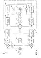
- FIGURE 1 a recovery loop 10 embodying the present invention.
- An incoming intermediate frequency data modulated signal (IF signal) is applied to the recovery loop 10 on line 12.
- the IF signal includes an IF carrier signal component having a design center frequency and also includes a data signal.
- a splitter 14 receives the IF signal and splits the signal into two channels. One channel signal is applied to a mixer 16 and the other channel signal is applied to a mixer 18.
- Mixers 16 and 18 are conventional analog mixers such as double balanced diode mixers.
- a temperature controlled oscillator 20 produces a fixed frequency signal at the design center frequency.
- the fixed frequency signal of the oscillator 20 is applied directly to the mixer 18 and is also applied to a 90° phase shifter 22.
- the output of the 90° phase shifter 22 is then applied to the mixer 16.
- the outputs of the mixers 16 and 18 constitute the quadrature components of the data signal with a frequency offset.
- the oscillator 20 is designed to produce a fixed frequency at the design center frequency of the IF carrier signal, there is no provision for locking the output of the temperature controlled oscillator 20 to the IF carrier signal. Thus, there exists a frequency offset between the output of the oscillator 20 and the IF carrier signal.
- the outputs of the mixers 16 and 18 include a high frequency component that is produced by the conventional mixers 16 and 18.
- the output of mixer 16 is applied through a low pass filter 24 to remove the high frequency component, and the output of the low pass filter 24 is applied to an analog-to-digital converter 26.
- the output of the mixer 18 is applied to a low pass filter 28 to remove the high frequency component, and the output of the low pass filter 28 is applied to an analog-to-digital converter 30.
- the outputs of the analog-to-digital converters 26 and 30 are digital representations of the data signal with the frequency offset.
- a digital complex multiplier 32 receives the output signals from the analog to digital converters 26 and 30, and multiplies such signals by a digital input received from a number controlled oscillator 34.
- the number controlled oscillator 34 is operable to produce signals representing both positive and negative frequencies.
- One output of the multiplier 32 is applied through a matched filter 36 whose output is applied to a limiter 38.
- the other output of the multiplier 32 is applied to a matched filter 40 whose output is applied to a limiter 42.
- the output of the matched filter 36 is applied to a digital mixer 44, and the other input of the digital mixer 44 is connected to the output of the limiter 42.
- the output of the matched filter 40 is also applied to a mixer 46, and the remaining input of the mixer 46 is connected to the output of the limiter 38.
- the outputs of the mixers 44 and 46 are applied to a summer 48 that digitally sums the two signals and provides a summation signal to the input of a loop filter 50.
- the output of the loop filter 50 is a control signal that is applied to the number control oscillator 34. In this manner, the number control oscillator 34 is locked or synchronized with the frequency offset that appears in the outputs of the analog-to-digital converters 26 and 30.
- the matched filters 36 and 40, the limiters 38 and 42, the mixers 44 and 46, the summer 48 and the loop filter 50 form a feedback loop or a phase lock loop for controlling the number control oscillator 34.
- the function of the temperature control oscillator 20 is to convert the frequency of the incoming IF signal on line 12 to a baseband frequency so that subsequent demodulation may be performed digitally at the lower baseband frequency.
- the output of the low pass filters 24 and 28 constitutes the quadrature components of the data signals with a frequency offset.
- the phrase "frequency offset" will be understood to include an arbitrary phase offset between the incoming IF carrier signal and the fixed frequency signal from the temperature control oscillator 20.
- the quadrature components produced at the output of the low pass filters 24 and 28 may be considered to be the components of a signal whose equation is: where
- the outputs of the number control oscillator 34 may be considered to be the components of a signal whose equation is:
- the complex multiplier then performs the operation: This multiplication gives the result e j ⁇ m.
- the result of the multiplication results in a data signal including only the phase.shift keying phase modulation.
- the multiplication in the complex multiplier 32 is done in the rectangular domain rather than the polar domain for convenience in processing.
- the quadrature components of the signal e j( ⁇ o t + ⁇ o + e m ) may be represented as cos ( ⁇ o t + ⁇ o + e m ) + j s i n ( Wo t + ⁇ o + e m) which may be simply represented as x + jy, where x and y represent the outputs of the analog-to-digital converters 26 and 30.
- all of the circuitry within the dotted line 52 is implemented digitally. Since the complex multiplier 32 must perform complicated multiplications at a relatively high speed, the multiplier is implemented as discrete T 2 L logic, and the remainder of the circuitry within the dotted line may be implemented as hardware, firmware or software in a computer.
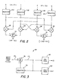
- FIGURE 2 A block diagram of the complex multiplier 32 is shown in FIGURE 2.
- Registers 54 and 56 receive inputs X and Y, respectively, which are digital numbers representing the quadrature components produced at the outputs of the analog-to-digital converters 26 and 30.
- Registers 58 and 60 receive inputs P and Q which represent the quadrature components produced at the outputs of the number control oscillator 34.
- the outputs of registers 54, 56, 58 and 60 correspond to their inputs and are used to perform complex multiplication.
- a mixer 62 receives the output from registers 54 and 58.
- a mixer 64 receives inputs from the outputs of registers 56 and 60.
- a mixer 66 receives inputs from the outputs of registers 56 and 58.
- a mixer 68 receives inputs from the outputs of registers 54 and 60.
- the output from the.mixer 64 is subtracted from the output of the mixer 62 in a subtractor 70.
- the output of the subtractor 70 represents the operation (XP - YQ).
- the outputs of the mixers 66 and 68 are added together in a summer 72, so that the output of the summer 72 represents the operation (j)(XQ + YP)).
- the outputs of the subtractor 70 and the summer 72 represent the complex number, (XP - YQ) +j (XQ + YP).
- this complex number is the data signal which includes the phase shift keying modulation.
- FIGURE 3 there is shown a block diagram of the number control oscillator 34.
- An input signal is received on line 74 from the loop filter 50 (FIGURE 1).
- the input signal is applied to a summer 76 that receives a second input from a register 78.
- the summer 76 sums its two inputs and produces an output signal on line 77.
- the output signal on line 77 is applied back to the register 78 and is also applied to select an address in read only memories 80 and 82.
- the read only memory 80 produces the sine of the desired output frequency as determined by the input signal on line 74, and the read only memory 82 produces the cosine of the desired output frequency.
- the output of the read only memory 80 corresponds to j Q and the output of the read only memory 82 corresponds to P as used above.
- the sum, P + jQ, is the complex number used in the complex multiplication in the multiplier 32 to demodulate or to remove the frequency offset from the outputs of the analog-to-digital converters 26 and 30.
- FIGURE 1 Two possible though not exhaustive implementations of loop filter 50 (FIGURE 1) are shown in FIGURES 4, 5a and 5b.
- a digital multiplier 90 is provided as the loop filter 50.
- the output of summer 48 is applied to one input of mixer 90 and a constant or variable gain signal is applied on line 92 to the other input.
- mixer 90 is a gain block providing a first order loop frequency response. Since the bandwidth of a first order loop is proportional to the total loop gain, the bandwidth may be varied by changing the gain signal on line 92.
- the embodiment shown in FIGURE 5b is an example of a digital implementation of the filter shown in FIGURE 5a.
- the circuitry of FIGURE 5b includes a summer 106 connected to the output of the mixer 96.
- the output of summer 106 is fed back through a register 108 to the remaining input of the summer 106. In this manner, the previous output of summer 106 is used in forming a new output.
- the summer 106 and register 108 function as a digital integrator.
- the output of the summer 106 is connected to an input of the summer 104.
- the remaining input of the summer 104 is connected to the mixer 94 as in the circuitry shown in FIGURE 5a.
- K 1 and K 2 are supplied respectively to mixers 94 and 96 on lines 98 and 100. These constants set the loop natural frequency and the damping factor in accordance with the following equations: and where:
Abstract
Description
- The present invention relates to carrier recovery loops for use in a demodulator, and particularly relates to a carrier recovery loop for digital implementation at baseband frequencies.
- Many types of carrier recovery loops for demodulating an incoming signal are well-known. in the art. In one type of conventional loop, known as a Costas type loop, a local oscillator is used to remove the carrier frequency from the incoming signal. Typically, the signal from the local oscillator is mixed with the incoming signal to produce one channel signal, and the local oscillator signal is phase shifted by 90° and is mixed with the incoming signal to produce a second channel signal. The two channel signals are then applied to a feedback loop that locks the local oscillator in synchronism with the incoming carrier frequency. The mixing of this local oscillator signal and the incoming signal will remove the carrier frequency from the incoming signal. In this manner, the local oscillator is used to demodulate the incoming signal. It will be appreciated that the local oscillator in a Costas type loop must produce varying frequencies in order to follow the frequency drift of the incoming signal.
- Because of the high data rate or frequency at which the Costas type loop must operate, it is not well suited for digital implementation. Therefore, a need has arisen for a carrier recovery loop for replacing a Costas type loop that is amenable to digital implementation. Specifically, a need has arisen for-a recovery loop that may be implemented digitally without the problems associated with digitally implementing a recovery loop at high frequencies at which Costas loops are normally operated.
- Analog demodulators often suffer from problems peculiar to analog devices such as D.C. offset and voltage controlled oscillator drift. A need has arisen - for a digitally implemented recovery loop to overcome such problems. Furthermore, analog demodulators are not flexible for being adapted to varying data rates and different forms of demodulation. With a digital recovery loop, loop parameters may be changed by software modification to allow operation at different data rates and forms of modulation such as phase shift keying and frequency shift keying. In addition, digital demodulation circuitry may be miniaturized using integrated circuits.
- In accordance with the present invention, a recovery loop demodulates a received data modulated signal to produce a data signal at a base band frequency. An analog circuit receives the data modulated signal and produces analog output signals corresponding to the data signals with a frequency offset component. The analog output signals are produced at approximately the baseband frequency. A processing circuit is responsive to the analog output signals to remove the frequency offset component to produce the data signal in digital form.
- In accordance with an embodiment of the present invention, the processing circuit is a digital processing circuit that includes a digital complex multiplier in which the data signal with a frequency offset component is multiplied by a first complex number. The first complex number represents positive or negative frequencies, and the complex multiplication i3 operable to cancel or remove the frequency offset to produce a complex product in digital form which corresponds to the data signal.
- In accordance with a particular embodiment of the invention, the analog circuit includes a splitter for splitting the received data modulated signal into first and second channels. A local oscillator produces a fixed frequency signal at a frequency approximating a design center frequency of the carrier signal of the data modulated signal, and a 901 phase shifter is responsive to the fixed frequency signal to produce a 90° phase shifted fixed frequency signal. A first analog mixer mixes the first channel signal with the 90° phase shifted fixed frequency signal to produce a first product signal. A second analog mixer mixes the second channel signal with the fixed frequency signal to produce a second product signal. The first and second product signals constitute the analog output signals that are applied to the processing circuit previously described.
- The present invention may be more fully understood by those of ordinary skill in the art by reference to the following Detailed Description when considered in conjunction with the Drawings in which:
- FIGURE 1 is a block diagram of a recovery loop embodying the present invention in which a temperature controlled oscillator and a digital complex multiplier are used to demodulate an incoming IF signal;
- FIGURE 2 is a diagram of the complex multiplier used in the present invention;
- FIGURE 3 is a block diagram of a complex number controlled oscillator used in the present invention for providing an input to the complex multiplier;
- FIGURE 4 shows a multiplier used as a loop filter having a first order frequency response; and
- FIGURES 5a and 5b show alternate loop filters having a second order frequency response.
- Referring now to the Drawings in which like reference characters designate like or corresponding parts throughout the several views, there is shown in FIGURE 1 a
recovery loop 10 embodying the present invention. An incoming intermediate frequency data modulated signal (IF signal) is applied to therecovery loop 10 online 12. The IF signal includes an IF carrier signal component having a design center frequency and also includes a data signal. Asplitter 14 receives the IF signal and splits the signal into two channels. One channel signal is applied to amixer 16 and the other channel signal is applied to amixer 18.Mixers - A temperature controlled
oscillator 20 produces a fixed frequency signal at the design center frequency. The fixed frequency signal of theoscillator 20 is applied directly to themixer 18 and is also applied to a 90°phase shifter 22. The output of the 90°phase shifter 22 is then applied to themixer 16. - The outputs of the
mixers oscillator 20 is designed to produce a fixed frequency at the design center frequency of the IF carrier signal, there is no provision for locking the output of the temperature controlledoscillator 20 to the IF carrier signal. Thus, there exists a frequency offset between the output of theoscillator 20 and the IF carrier signal. - In addition to the data signal with a frequency offset, the outputs of the
mixers conventional mixers mixer 16 is applied through alow pass filter 24 to remove the high frequency component, and the output of thelow pass filter 24 is applied to an analog-to-digital converter 26. Likewise, the output of themixer 18 is applied to alow pass filter 28 to remove the high frequency component, and the output of thelow pass filter 28 is applied to an analog-to-digital converter 30. - The outputs of the analog-to-
digital converters 26 and 30 are digital representations of the data signal with the frequency offset. Adigital complex multiplier 32 receives the output signals from the analog todigital converters 26 and 30, and multiplies such signals by a digital input received from a number controlledoscillator 34. The number controlledoscillator 34 is operable to produce signals representing both positive and negative frequencies. When the output from the number controlledoscillator 34 is multiplied by the quadrature components of the data signals with the frequency offset in thecomplex multiplier 32, the frequency offset is removed and the output of thecomplex multiplier 32 represents the quadrature components of the data signals in digital form. - One output of the
multiplier 32 is applied through a matchedfilter 36 whose output is applied to alimiter 38. The other output of themultiplier 32 is applied to a matchedfilter 40 whose output is applied to alimiter 42. The output of the matchedfilter 36 is applied to adigital mixer 44, and the other input of thedigital mixer 44 is connected to the output of thelimiter 42. The output of the matchedfilter 40 is also applied to amixer 46, and the remaining input of themixer 46 is connected to the output of thelimiter 38. - The outputs of the
mixers summer 48 that digitally sums the two signals and provides a summation signal to the input of aloop filter 50. The output of theloop filter 50 is a control signal that is applied to thenumber control oscillator 34. In this manner, thenumber control oscillator 34 is locked or synchronized with the frequency offset that appears in the outputs of the analog-to-digital converters 26 and 30. The matched filters 36 and 40, thelimiters mixers summer 48 and theloop filter 50 form a feedback loop or a phase lock loop for controlling thenumber control oscillator 34. - In operation, the function of the
temperature control oscillator 20 is to convert the frequency of the incoming IF signal online 12 to a baseband frequency so that subsequent demodulation may be performed digitally at the lower baseband frequency. After the incoming IF signal is mixed inmixers filters temperature control oscillator 20. - The quadrature components produced at the output of the low pass filters 24 and 28 may be considered to be the components of a signal whose equation is:

- ωo = The deviation in frequency between the incoming IF carrier signal and the fixed frequency signal of the
temperature control oscillator 20 caused by offsets in the IF signal such as doppler shifts. - θo = An arbitrary phase offset between the incoming IF carrier signal and the fixed frequency signal of the
oscillator 20. - θm = The phase shift keying phase modulation.
- The outputs of the
number control oscillator 34 may be considered to be the components of a signal whose equation is:

- As will be hereinafter described in more detail, the multiplication in the
complex multiplier 32 is done in the rectangular domain rather than the polar domain for convenience in processing. The quadrature components of the signal ej(ωo t + θo + e m) may be represented as cos (ωot + θo + em) + j sin (Wo t + θo + em) which may be simply represented as x + jy, where x and y represent the outputs of the analog-to-digital converters 26 and 30. Where P and Q represent the outputs of thenumber control oscillator 34, the multiplication performed by thecomplex multiplier 32 may be represented as: (X + jY) (P + jQ) = (XP-YQ) + j(XQ + PY). - In the preferred embodiment, all of the circuitry within the dotted
line 52 is implemented digitally. Since thecomplex multiplier 32 must perform complicated multiplications at a relatively high speed, the multiplier is implemented as discrete T2L logic, and the remainder of the circuitry within the dotted line may be implemented as hardware, firmware or software in a computer. - A block diagram of the
complex multiplier 32 is shown in FIGURE 2.Registers digital converters 26 and 30.Registers number control oscillator 34. The outputs ofregisters - A
mixer 62 receives the output fromregisters mixer 64 receives inputs from the outputs ofregisters mixer 66 receives inputs from the outputs ofregisters mixer 68 receives inputs from the outputs ofregisters - The output from
the.mixer 64 is subtracted from the output of themixer 62 in asubtractor 70. Thus, the output of thesubtractor 70 represents the operation (XP - YQ). - The outputs of the
mixers summer 72, so that the output of thesummer 72 represents the operation (j)(XQ + YP)). Thus, the outputs of thesubtractor 70 and thesummer 72 represent the complex number, (XP - YQ) +j (XQ + YP). As previously described, this complex number is the data signal which includes the phase shift keying modulation. - Referring now to FIGURE 3, there is shown a block diagram of the
number control oscillator 34. An input signal is received online 74 from the loop filter 50 (FIGURE 1). The input signal is applied to asummer 76 that receives a second input from aregister 78. Thesummer 76 sums its two inputs and produces an output signal online 77. The output signal online 77 is applied back to theregister 78 and is also applied to select an address in read onlymemories - Data has been loaded into the
memories memory 80 produces the sine of the desired output frequency as determined by the input signal online 74, and the read onlymemory 82 produces the cosine of the desired output frequency. Thus, the output of the read onlymemory 80 corresponds to jQ and the output of the read onlymemory 82 corresponds to P as used above. The sum, P + jQ, is the complex number used in the complex multiplication in themultiplier 32 to demodulate or to remove the frequency offset from the outputs of the analog-to-digital converters 26 and 30. - Two possible though not exhaustive implementations of loop filter 50 (FIGURE 1) are shown in FIGURES 4, 5a and 5b. In FIGURE 4, a
digital multiplier 90 is provided as theloop filter 50. The output ofsummer 48 is applied to one input ofmixer 90 and a constant or variable gain signal is applied online 92 to the other input. Thus,mixer 90 is a gain block providing a first order loop frequency response. Since the bandwidth of a first order loop is proportional to the total loop gain, the bandwidth may be varied by changing the gain signal online 92. - In FIGURE 5A, a second order loop frequency implementation of
loop filter 50 is shown. In this embodiment, the output ofsummer 48 is applied to inputs ofmixers mixers mixer 96 is applied to anintegrator 102 for cummulatively integrating the output of themixer 96, and the outputs of theintegrator 102 and themixer 94 are applied to asummer 104 that produces the output of the loop-filter 50 online 74. - The embodiment shown in FIGURE 5b is an example of a digital implementation of the filter shown in FIGURE 5a. The circuitry of FIGURE 5b includes a
summer 106 connected to the output of themixer 96. The output ofsummer 106 is fed back through aregister 108 to the remaining input of thesummer 106. In this manner, the previous output ofsummer 106 is used in forming a new output. Thesummer 106 and register 108 function as a digital integrator. The output of thesummer 106 is connected to an input of thesummer 104. The remaining input of thesummer 104 is connected to themixer 94 as in the circuitry shown in FIGURE 5a. - The constants, K1 and K2, are supplied respectively to
mixers lines 98 and 100. These constants set the loop natural frequency and the damping factor in accordance with the following equations:

- (zeta) is the desired loop damping factor;
- wn is the desired loop frequency in radian frequency; and
- KT is the total loop gain.
- Although a particular embodiment has been described in the foregoing Detailed Description, it will be understood that the invention is capable of numerous rearrangements, modifications and substitution of parts without departing from the spirit of the invention. In particular, although phase shift keying modulation was discussed in association with the above-described embodiment, it will be understood that the present invention may be implemented using other forms of modulation.
Claims (12)
Applications Claiming Priority (2)
| Application Number | Priority Date | Filing Date | Title |
|---|---|---|---|
| US06/110,462 US4348641A (en) | 1980-01-08 | 1980-01-08 | Digital baseband carrier recovery circuit |
| US110462 | 1980-01-08 |
Publications (2)
| Publication Number | Publication Date |
|---|---|
| EP0032253A1 true EP0032253A1 (en) | 1981-07-22 |
| EP0032253B1 EP0032253B1 (en) | 1984-08-15 |
Family
ID=22333143
Family Applications (1)
| Application Number | Title | Priority Date | Filing Date |
|---|---|---|---|
| EP80108261A Expired EP0032253B1 (en) | 1980-01-08 | 1980-12-31 | Demodulator carrier recovery loop and method for demodulating a signal |
Country Status (6)
| Country | Link |
|---|---|
| US (1) | US4348641A (en) |
| EP (1) | EP0032253B1 (en) |
| JP (1) | JPS56146346A (en) |
| CA (1) | CA1162619A (en) |
| DE (1) | DE3068980D1 (en) |
| DK (1) | DK161287C (en) |
Cited By (8)
| Publication number | Priority date | Publication date | Assignee | Title |
|---|---|---|---|---|
| EP0084876A2 (en) * | 1982-01-25 | 1983-08-03 | International Standard Electric Corporation | Demodulator arrangement for signals which are frequency-modulated on a carrier wave |
| GB2153635A (en) * | 1984-01-09 | 1985-08-21 | Clarion Co Ltd | Psk demodulator |
| FR2643765A1 (en) * | 1989-02-27 | 1990-08-31 | Meuriche Bernard | DECOMPOSITION DEVICE WITH OPTIMUM SAMPLING RATE OF A BANDWIDTH SIGNAL IN ITS COMPONENTS ON TWO CARRIERS IN QUADRATURE |
| EP0481543A1 (en) * | 1990-10-01 | 1992-04-22 | Philips Electronics Uk Limited | Filtering arrangement |
| EP0535638A2 (en) * | 1991-09-30 | 1993-04-07 | Nec Corporation | Phase divider for complex signals |
| EP0535591A2 (en) * | 1991-09-30 | 1993-04-07 | Nec Corporation | Phase-locked circuit capable of being quickly put in a phase locked state |
| WO1996012367A1 (en) * | 1994-10-13 | 1996-04-25 | Westinghouse Electric Corporation | Carrier tracking loop for qpsk demodulator |
| GB2311194A (en) * | 1996-03-12 | 1997-09-17 | Nokia Mobile Phones Ltd | Transmitting and receiving radio signals |
Families Citing this family (16)
| Publication number | Priority date | Publication date | Assignee | Title |
|---|---|---|---|---|
| US4501002A (en) * | 1983-02-28 | 1985-02-19 | Auchterlonie Richard C | Offset QPSK demodulator and receiver |
| US4608540A (en) * | 1983-07-04 | 1986-08-26 | Clarion Co., Ltd. | Phase-shift keying demodulator |
| GB2153177B (en) * | 1984-01-19 | 1987-06-03 | Standard Telephones Cables Ltd | Digital navstar receiver |
| US5223843A (en) * | 1988-01-05 | 1993-06-29 | Rockwell International Corporation | High performance global positioning system receiver means and method |
| JPH01274548A (en) * | 1988-04-26 | 1989-11-02 | Nec Corp | Demodulator |
| JPH03278745A (en) * | 1990-03-28 | 1991-12-10 | Matsushita Electric Ind Co Ltd | Frequency deviation detector |
| US5287388A (en) * | 1991-06-25 | 1994-02-15 | Kabushiki Kaisha Toshiba | Frequency offset removal method and apparatus |
| US5304957A (en) * | 1992-10-01 | 1994-04-19 | Westinghouse Electric Corp. | Low jitter phase locked loop for single phase applications |
| SE502813C2 (en) * | 1994-05-04 | 1996-01-22 | Ericsson Telefon Ab L M | Method and device for analog-digital converters |
| DE19536526A1 (en) * | 1995-09-29 | 1997-04-03 | Siemens Ag | Receiver architecture for receiving angle-modulated / keyed carrier signals of different frequencies |
| US5995563A (en) * | 1997-02-10 | 1999-11-30 | Lsi Logic Corporation | System and method for fast channel switching in a satellite receiver |
| US6337885B1 (en) * | 1998-02-13 | 2002-01-08 | Telefonaktiebolaget Lm Ericsson (Publ) | Radio receiver that digitizes a received signal at a plurality of digitization frequencies |
| US6873663B1 (en) | 2000-02-16 | 2005-03-29 | Telefonaktiebolaget Lm Ericsson | Reception of M-ary PSK-modulated signals |
| JP2006326590A (en) * | 2005-05-23 | 2006-12-07 | Sintokogio Ltd | Remote monitoring system for mold making apparatus |
| US8033316B2 (en) * | 2005-06-07 | 2011-10-11 | Sintokogio, Ltd. | Flask unit and cope-and-drag molding machine and line |
| EP3759883A4 (en) * | 2018-03-01 | 2021-10-20 | Telefonaktiebolaget Lm Ericsson (Publ) | Methods and apparatus for signal demodulation |
Citations (8)
| Publication number | Priority date | Publication date | Assignee | Title |
|---|---|---|---|---|
| US3983499A (en) * | 1974-09-25 | 1976-09-28 | Nippon Electric Company, Ltd. | Multi-phase PSK demodulator |
| US4076956A (en) * | 1975-03-27 | 1978-02-28 | Cselt - Centro Studi E Laboratori Telecomunicazioni | Decision network for receiver of PSK digital signals |
| US4085378A (en) * | 1975-06-11 | 1978-04-18 | Motorola, Inc. | QPSK demodulator |
| DE2735945A1 (en) * | 1976-10-18 | 1978-04-20 | Ibm | CIRCUIT ARRANGEMENT FOR THE CARRIER SYNCHRONIZATION OF COAERENT PHASE DEMODULATORS |
| US4092606A (en) * | 1977-06-21 | 1978-05-30 | Lovelace Alan M Acting Adminis | Quadraphase demodulation |
| US4105975A (en) * | 1977-02-01 | 1978-08-08 | Ncr Corporation | Offset correction circuit for phase detectors |
| GB1527732A (en) * | 1976-07-15 | 1978-10-11 | Micro Consultants Ltd | Digital phase locked loop |
| US4143322A (en) * | 1976-09-30 | 1979-03-06 | Nippon Electric Co., Ltd. | Carrier wave recovery system apparatus using synchronous detection |
Family Cites Families (13)
| Publication number | Priority date | Publication date | Assignee | Title |
|---|---|---|---|---|
| US3101448A (en) * | 1954-12-23 | 1963-08-20 | Gen Electric | Synchronous detector system |
| US3204185A (en) * | 1961-04-19 | 1965-08-31 | North American Aviation Inc | Phase-lock receivers |
| US3403355A (en) * | 1966-01-12 | 1968-09-24 | Fujitsu Ltd | Phase control circuit |
| US3368036A (en) * | 1965-05-24 | 1968-02-06 | Collins Radio Co | Demultiplexing and detecting system for predicted wave phasepulsed data transmissionsystem |
| US3500217A (en) * | 1967-07-31 | 1970-03-10 | Us Navy | Frequency discriminator employing quadrature demodulation techniques |
| US3568067A (en) * | 1969-06-13 | 1971-03-02 | Collins Radio Co | Frequency discriminator with output indicative of difference between input and local reference signals |
| US3745255A (en) * | 1971-08-18 | 1973-07-10 | J Fletcher | Receiver with an improved phase lock loop in a multichannel telemetry system with suppressed carrier |
| US3768030A (en) * | 1972-05-08 | 1973-10-23 | Motorola Inc | Automatic signal acquisition means for phase-lock loop with anti- sideband lock protection |
| US3787775A (en) * | 1973-03-28 | 1974-01-22 | Trw Inc | Phase correction circuit |
| US3789316A (en) * | 1973-06-13 | 1974-01-29 | Singer Co | Sine-cosine frequency tracker |
| US3893039A (en) * | 1974-05-02 | 1975-07-01 | Us Navy | Two-channel phase-locked loop |
| US3993956A (en) * | 1975-11-03 | 1976-11-23 | Motorola, Inc. | Digital detection system for differential phase shift keyed signals |
| JPS5917916B2 (en) * | 1975-12-26 | 1984-04-24 | 日本電気株式会社 | Isoudouukisouchi |
-
1980
- 1980-01-08 US US06/110,462 patent/US4348641A/en not_active Expired - Lifetime
- 1980-12-30 CA CA000367682A patent/CA1162619A/en not_active Expired
- 1980-12-31 DE DE8080108261T patent/DE3068980D1/en not_active Expired
- 1980-12-31 EP EP80108261A patent/EP0032253B1/en not_active Expired
-
1981
- 1981-01-06 DK DK003181A patent/DK161287C/en active
- 1981-01-08 JP JP83081A patent/JPS56146346A/en active Granted
Patent Citations (8)
| Publication number | Priority date | Publication date | Assignee | Title |
|---|---|---|---|---|
| US3983499A (en) * | 1974-09-25 | 1976-09-28 | Nippon Electric Company, Ltd. | Multi-phase PSK demodulator |
| US4076956A (en) * | 1975-03-27 | 1978-02-28 | Cselt - Centro Studi E Laboratori Telecomunicazioni | Decision network for receiver of PSK digital signals |
| US4085378A (en) * | 1975-06-11 | 1978-04-18 | Motorola, Inc. | QPSK demodulator |
| GB1527732A (en) * | 1976-07-15 | 1978-10-11 | Micro Consultants Ltd | Digital phase locked loop |
| US4143322A (en) * | 1976-09-30 | 1979-03-06 | Nippon Electric Co., Ltd. | Carrier wave recovery system apparatus using synchronous detection |
| DE2735945A1 (en) * | 1976-10-18 | 1978-04-20 | Ibm | CIRCUIT ARRANGEMENT FOR THE CARRIER SYNCHRONIZATION OF COAERENT PHASE DEMODULATORS |
| US4105975A (en) * | 1977-02-01 | 1978-08-08 | Ncr Corporation | Offset correction circuit for phase detectors |
| US4092606A (en) * | 1977-06-21 | 1978-05-30 | Lovelace Alan M Acting Adminis | Quadraphase demodulation |
Non-Patent Citations (4)
| Title |
|---|
| IEEE TRANSACTIONS ON COMMUNICATIONS, Vol. Com. 26, No. 1, January 1978 K. FEHER et al. "A New Symbol Timing Recovery Technique for Burst Modem Aplications" pages 100 to 108 * |
| IEEE TRANSACTIONS ON COMMUNICATIONS, Vol. Com. 26, No. 5, May 1978 CH.R. HOGGE "Carrier and Clock Recovery for 8 PSK Synchoronous Demodulation" pages 528 to 533 * |
| IEEE TRANSACTIONS ON COMMUNICATIONS, Vol. Com. 26, No. 6, June 1978 M.K. SIMON"Optimum Receiver Structure for Phase-Multiplexed Modulations" pages 865 to 872 * |
| IEEE TRANSACTIONS ON COMMUNICATIONS, Vol. Com. 27, No. 2, February 1979 D.P. TAYLOR et al."A Decision-Directed Carrier Recovery Loop for Duobinary Encoded Offset QPSK Signals" pages 461 to 468 * |
Cited By (15)
| Publication number | Priority date | Publication date | Assignee | Title |
|---|---|---|---|---|
| EP0084876A2 (en) * | 1982-01-25 | 1983-08-03 | International Standard Electric Corporation | Demodulator arrangement for signals which are frequency-modulated on a carrier wave |
| EP0084876A3 (en) * | 1982-01-25 | 1985-10-23 | International Standard Electric Corporation | Demodulator arrangement for signals which are frequency-modulated on a carrier wave |
| GB2153635A (en) * | 1984-01-09 | 1985-08-21 | Clarion Co Ltd | Psk demodulator |
| FR2643765A1 (en) * | 1989-02-27 | 1990-08-31 | Meuriche Bernard | DECOMPOSITION DEVICE WITH OPTIMUM SAMPLING RATE OF A BANDWIDTH SIGNAL IN ITS COMPONENTS ON TWO CARRIERS IN QUADRATURE |
| US5056115A (en) * | 1989-02-27 | 1991-10-08 | Bernard Meuriche | Device for the division, at an optimum sampling rate, of a passband signal into its components on two carriers in quadrature |
| EP0481543A1 (en) * | 1990-10-01 | 1992-04-22 | Philips Electronics Uk Limited | Filtering arrangement |
| EP0535638A2 (en) * | 1991-09-30 | 1993-04-07 | Nec Corporation | Phase divider for complex signals |
| EP0535591A2 (en) * | 1991-09-30 | 1993-04-07 | Nec Corporation | Phase-locked circuit capable of being quickly put in a phase locked state |
| EP0535591A3 (en) * | 1991-09-30 | 1993-05-12 | Nec Corporation | Phase-locked circuit capable of being quickly put in a phase locked state |
| EP0535638A3 (en) * | 1991-09-30 | 1993-08-04 | Nec Corporation | Phase divider for complex signals |
| WO1996012367A1 (en) * | 1994-10-13 | 1996-04-25 | Westinghouse Electric Corporation | Carrier tracking loop for qpsk demodulator |
| GB2311194A (en) * | 1996-03-12 | 1997-09-17 | Nokia Mobile Phones Ltd | Transmitting and receiving radio signals |
| EP0795978A3 (en) * | 1996-03-12 | 1999-07-21 | Nokia Mobile Phones Ltd. | Frequency control for frequency division channels |
| GB2311194B (en) * | 1996-03-12 | 2000-05-31 | Nokia Mobile Phones Ltd | Transmitting and receiving radio signals |
| US6091780A (en) * | 1996-03-12 | 2000-07-18 | Nokia Mobile Phones, Ltd. | Transmitting and receiving radio signals |
Also Published As
| Publication number | Publication date |
|---|---|
| EP0032253B1 (en) | 1984-08-15 |
| JPS56146346A (en) | 1981-11-13 |
| CA1162619A (en) | 1984-02-21 |
| DK161287C (en) | 1991-12-09 |
| DK161287B (en) | 1991-06-17 |
| US4348641A (en) | 1982-09-07 |
| JPS6348469B2 (en) | 1988-09-29 |
| DE3068980D1 (en) | 1984-09-20 |
| DK3181A (en) | 1981-07-09 |
Similar Documents
| Publication | Publication Date | Title |
|---|---|---|
| US4348641A (en) | Digital baseband carrier recovery circuit | |
| US4509017A (en) | Method and apparatus for pulse angle modulation | |
| US5263196A (en) | Method and apparatus for compensation of imbalance in zero-if downconverters | |
| EP0877476B1 (en) | Down conversion mixer | |
| US5268647A (en) | Method and arrangement of coherently demodulating PSK signals using a feedback loop including a filter bank | |
| US5301210A (en) | Coherent demodulating device with carrier wave recovering digital circuit | |
| US4682117A (en) | Quadrature demodulation data receiver with phase error correction | |
| US4599743A (en) | Baseband demodulator for FM and/or AM signals | |
| US4766392A (en) | Demodulating an angle-modulated signal | |
| US4677690A (en) | Baseband demodulator for FM and/or AM signals | |
| US4485358A (en) | Method and apparatus for pulse angle modulation | |
| EP0083236B1 (en) | Carrier recovery circuit | |
| WO2001058103A2 (en) | Kaskadenfrequenzumsetzer unter verwendung von phasenverschobenen signalen der lokalen oszillatoren | |
| US4833416A (en) | QPSK/BPSK demodulator | |
| GB2188517A (en) | Spread-spectrum receivers | |
| US3108158A (en) | Synchronous detection multiplex system | |
| JP2765601B2 (en) | Demodulation circuit | |
| GB2318229A (en) | Costas loop carrier recovery circuit | |
| JPS6331985B2 (en) | ||
| JPH0358546A (en) | Phase comparator circuit | |
| JP2837914B2 (en) | AFC device | |
| JPH06105898B2 (en) | Interference compensation circuit | |
| JP2705363B2 (en) | Automatic interference canceller | |
| KR100285756B1 (en) | Apparatus for tracking carrier in wireless transfer system | |
| JPH06103893B2 (en) | Digital phase modulator |
Legal Events
| Date | Code | Title | Description |
|---|---|---|---|
| PUAI | Public reference made under article 153(3) epc to a published international application that has entered the european phase |
Free format text: ORIGINAL CODE: 0009012 |
|
| AK | Designated contracting states |
Designated state(s): BE DE FR GB NL SE |
|
| RBV | Designated contracting states (corrected) |
Designated state(s): BE DE FR GB NL SE |
|
| 17P | Request for examination filed |
Effective date: 19811007 |
|
| GRAA | (expected) grant |
Free format text: ORIGINAL CODE: 0009210 |
|
| AK | Designated contracting states |
Designated state(s): BE DE FR GB NL SE |
|
| REF | Corresponds to: |
Ref document number: 3068980 Country of ref document: DE Date of ref document: 19840920 |
|
| ET | Fr: translation filed | ||
| PLBE | No opposition filed within time limit |
Free format text: ORIGINAL CODE: 0009261 |
|
| STAA | Information on the status of an ep patent application or granted ep patent |
Free format text: STATUS: NO OPPOSITION FILED WITHIN TIME LIMIT |
|
| 26N | No opposition filed | ||
| PGFP | Annual fee paid to national office [announced via postgrant information from national office to epo] |
Ref country code: SE Payment date: 19921214 Year of fee payment: 13 |
|
| PGFP | Annual fee paid to national office [announced via postgrant information from national office to epo] |
Ref country code: NL Payment date: 19921231 Year of fee payment: 13 |
|
| PGFP | Annual fee paid to national office [announced via postgrant information from national office to epo] |
Ref country code: BE Payment date: 19930127 Year of fee payment: 13 |
|
| PG25 | Lapsed in a contracting state [announced via postgrant information from national office to epo] |
Ref country code: BE Effective date: 19931231 |
|
| PG25 | Lapsed in a contracting state [announced via postgrant information from national office to epo] |
Ref country code: SE Effective date: 19940101 |
|
| BERE | Be: lapsed |
Owner name: E-SYSTEMS INC. Effective date: 19931231 |
|
| PG25 | Lapsed in a contracting state [announced via postgrant information from national office to epo] |
Ref country code: NL Effective date: 19940701 |
|
| NLV4 | Nl: lapsed or anulled due to non-payment of the annual fee | ||
| EUG | Se: european patent has lapsed |
Ref document number: 80108261.1 Effective date: 19940810 |
|
| PGFP | Annual fee paid to national office [announced via postgrant information from national office to epo] |
Ref country code: FR Payment date: 19951212 Year of fee payment: 16 |
|
| PGFP | Annual fee paid to national office [announced via postgrant information from national office to epo] |
Ref country code: GB Payment date: 19951222 Year of fee payment: 16 Ref country code: DE Payment date: 19951222 Year of fee payment: 16 |
|
| PG25 | Lapsed in a contracting state [announced via postgrant information from national office to epo] |
Ref country code: GB Effective date: 19961231 |
|
| GBPC | Gb: european patent ceased through non-payment of renewal fee |
Effective date: 19961231 |
|
| PG25 | Lapsed in a contracting state [announced via postgrant information from national office to epo] |
Ref country code: FR Effective date: 19970829 |
|
| PG25 | Lapsed in a contracting state [announced via postgrant information from national office to epo] |
Ref country code: DE Effective date: 19970902 |
|
| REG | Reference to a national code |
Ref country code: FR Ref legal event code: ST |