EP0059349B1 - Display system with multiple scrolling regions - Google Patents
Display system with multiple scrolling regions Download PDFInfo
- Publication number
- EP0059349B1 EP0059349B1 EP19820101013 EP82101013A EP0059349B1 EP 0059349 B1 EP0059349 B1 EP 0059349B1 EP 19820101013 EP19820101013 EP 19820101013 EP 82101013 A EP82101013 A EP 82101013A EP 0059349 B1 EP0059349 B1 EP 0059349B1
- Authority
- EP
- European Patent Office
- Prior art keywords
- display
- data
- character
- row
- memory
- Prior art date
- Legal status (The legal status is an assumption and is not a legal conclusion. Google has not performed a legal analysis and makes no representation as to the accuracy of the status listed.)
- Expired
Links
Images


Classifications
-
- G—PHYSICS
- G09—EDUCATION; CRYPTOGRAPHY; DISPLAY; ADVERTISING; SEALS
- G09G—ARRANGEMENTS OR CIRCUITS FOR CONTROL OF INDICATING DEVICES USING STATIC MEANS TO PRESENT VARIABLE INFORMATION
- G09G5/00—Control arrangements or circuits for visual indicators common to cathode-ray tube indicators and other visual indicators
- G09G5/14—Display of multiple viewports
-
- G—PHYSICS
- G09—EDUCATION; CRYPTOGRAPHY; DISPLAY; ADVERTISING; SEALS
- G09G—ARRANGEMENTS OR CIRCUITS FOR CONTROL OF INDICATING DEVICES USING STATIC MEANS TO PRESENT VARIABLE INFORMATION
- G09G1/00—Control arrangements or circuits, of interest only in connection with cathode-ray tube indicators; General aspects or details, e.g. selection emphasis on particular characters, dashed line or dotted line generation; Preprocessing of data
- G09G1/007—Circuits for displaying split screens
Definitions
- This invention relates generally to data display system as defined in the precharacterising part of claim 1.
- a data display system has been advanced for forming a plurality of independently controllable display regions on a display device.
- This system has a data processor connected to a main memory.
- An input is connected to the data processor connected to the main memory display, and a data controller is connected to the data processor display memory wherein each row of characters to be displayed on the display device is assigned one or more memory location identifiers as defined by the display controller to indicate the display memory address of a subsequent row of characters to be displayed and wherein the display controller alters the sequence of rows displayed on the display device by modifying the memory location identifiers of the selected rows of characters.
- Another object is to provide a system for controlling a display memory which minimizes the processing load on a system CPU.
- Still another object is to provide a system for mapping the contents of a display memory without requiring the transfer of blocks of data therein during various editing anascrórr functions.
- Yet another object is to provide a display control system which may be formatted either locally or from a remote host computer.
- Another object is to provide the system microprocessor with executable instructions at a high access rate, and to provide the microprocessor with instructions through a directly accessed memory whose capacity is less than the list of program instructions.
- a microprocessor controls the system operation in accordance with the list of instructions stored in a random access main memory.
- the main memory stores a portion of the list of instructions, while the complete list of instructions is stored in a mass data storage memory in the form of one or more GROMs.
- An additional ROM contains a list of instructions for initializing the system and a nonvolatile memory in the form of a CMOS RAM powered by a battery is included to store system configuration parameters in the event of a power loss.
- a display device such as a CRT is controlled by a display control system formed of a CRT controller, a visual attribute generator, a display memory, and a character ROM. Alternate character sets are provided by a character RAM which is accessed by the display controller through the attribute generator.
- the display controller accesses the display memory asynchronously with the system microprocessor, thus decreasing the processing time and increasing the processor throughput. Segmentation of the display into multiple horizontal and vertical split regions which are independently scrollable either discretely or smoothly is provided by the linking of one or more row attribute bytes or "pointers" to each character and character attribute row stored in the display memory. In this manner, data can be manipulated on the display screen without changing the absolute address of the data in display memory. That is, only the pointers associated with each block of data (corresponding to a displayed row) needs to be modified by the display controller. Processing time is greatly reduced because whole blocks of data need not be transferred in the display memory, only the display memory addresses associated with the pointers are affected.
- input/output means are provided for communicating with a controller or "host" computer.
- input means in the form of a keyboard are provided.
- the keyboard is a self-contained unit having a dedicated microcomputer.
- the keyboard unit communicates with the system through a keyboard interface unit that converts the serial data into a parallel form which is processed by the system microprocessor.
- Discrete control of the display device contrast is achieved by a contrast register in conjunction with the attribute generator.
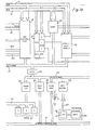
- a system microprocessor CPU 10 is coupled to a system control bus 12 and a system address bus 14.
- Control bus 12 and address bus 14 both extend to a counter time circuit CTC 18, a dual asynchronous transmitter/receiver DART 20, a serial input/output device SIO 22, a dynamic random-access memory (DRAM) timer 24 and a memory I/O decoder 26.
- System address 14 also extends to a system read-only memory (ROM) 27, a DRAM address multiplexer 28, a test ROM 29, a CMOS RAM 30, and a control I/O device 32.
- a battery 31 is coupled to CMOS RAM 30 to provide backup during power off conditions.
- CPU 10 is connected through a two-way buffer for transceiver (XCVR) 34 to a system data bus 36.
- Data bus 36 extends to a contrast register 38, and to CRTC 16, CRTC 18, DART 20, and SIO 22.
- Data bus 36 is connected through a transceiver 40 to a memory data bus 42 which in turn extends to system ROM 27 and a series of DRAMs 48a-48c.
- Each DRAM is also connected to DRAM timer 24 and to a DRAM address bus 50 which is connected to a DRAM multiplexer 28.
- Data bus 36 is also connected through a XCVR 44 to an I/O data bus 46 which in turn extends to test ROM 29, CMOS RAM 30, and control I/O 32.
- Program storage is provided by large scale mass read-only memory in the form of GROMs 52-1 to 52-8.
- the GROMs are connected to a common GROM bus 54 which is in turn connected to I/O data bus 46 through a GROM I/F 56.
- keyboard 58 An operator interfaces with the present system by means of a keyboard 58 which is connected to a keyboard I/F 60 through a telephone type multiconductor cable 62.
- Keyboard 58 contains its own computer 64 which permits keyboard 58 to process instructions with a minimum computing load on .CPU 10.
- a series of test multiplexers 66, 68, and 70 are connected respectively to DART 20, and channels B and A of SIO 22, to provide loop back testing of the terminal in a local operating mode.
- a set of communication buses 72, 74, and 76 are connected to control I/O 32 and, respectively, to test multiplexers 66, 68, and 70.
- Communication to peripheral devices such as printers is provided from communication buses 72 and 74 through EIA driver-receivers 78 and 80, which are connected respectively to auxiliary ports AUX 2 and AUX 1.
- Communication with a host computer is provided by communication bus 76 which is connected through a PM interface 82 and an EIA driver-receiver 84 to an input/output port labeled HOST in the drawing.
- a baud rate multiplexer 86 is connected to communication bus 76 and to control I/O 32 to provide synchronization and a selection of baud rates with the host computer.
- the timing of baud multiplexer 86 is provided by timer 18-0 of CTC 18.
- Baud rate timing for the AUX 2 and AUX 1 ports is provided by timers 18-2 and 18-1 of CTC 18.
- Timer 18-3 functions as a system timer.
- a communications option unit 87 shown by dashed lines in Figure 1c, is connected to the HOST port, the system address bus 14 and through an option I/F 88 to communication bus 76.
- Unit 87 is used to provide local and current-loop communications by methods known in the art, and need not be described in detail here.
- the present terminal communicates with an operator by video display means such as a CRT (not shown) which is driven by a controller CRTC 16.
- video display means such as a CRT (not shown) which is driven by a controller CRTC 16.
- the generation of characters with various character attributes will be described in more detail below. Briefly, however, a set of characters is stored in a character ROM 90 connected to CRTC 16 by a character bus 92.
- the character, along with selected visual "attributes" generated by a video attribute generator VAG 94 are stored in RAM display memory 96, which is connected to CRTC 16 through a register/buffer 98.
- an "attribute" is defined to mean any of the following in relation to individual characters:
- FIG. 2 there is shown a memory map of the present system illustrating the assigned memory of the various memory devices in hexadecimal form.
- memory locations 0000-7FFF In the basic 8-bit bytes in memory locations 0000-7FFF, and is expandable to 64K bytes in memory locations 8000-FFFF by the addition of DRAMs 48b and 48c.
- Memory locations 0000-1FFF are assigned to system ROM 27, which contains 2K bytes (expandable to 8K) of program instructions to control the system initialization and diagnostics on power up, as well as instructions for loading DRAM 48a from the program storage memory resident in the GROMs. DRAM 48a is used by CPU 10 for execution of instructions to control the terminal.
- Test ROM 29 48K byte maximum
- diagnostic aids such as signature analysis.
- Address 3000 is a write-only memory location that stores data in contrast register 38 to control the intensity level of the CRT as set by the operator.
- the attributes video on/off, background select, and highlight select are also controlled by register 38.
- a read at memory location 3A00 inputs the data sent by keyboard 58 and resets its associated interrupt.
- a write to this location sends data to the keyboard for processing.
- Read and write commands to memory locations 3A80-3A87 communicate the terminal configuration from control I/O 32 to CPU 10, that is, which of the basic and expandable devices are installed, as well as configuring the operational mode of the various communication devices are selected by the operator.
- Location 3BOO is reserved for communication option unit 87, which functions as described above.
- CMOS RAM 30 stores terminal configuration information such as communications baud rates so that the terminal can readily communicate with the host computer when power is restored.
- Display memory 96 which stores characters and associated attributes for display on the CRT screen, is accessed through CRT controller 16 as an I/O device.
- Display memory 96 contains 2K 16-bit bytes and is expandable to 8K in 2K increments.
- the GROM storage memory is accessed by addressing the GROM I/F 56 at memory location 3B80.
- a read from this location inputs 4 bits of data from the selected GROM, and a write to this memory location outputs address and control information for accessing the GROM.
- three 16K byte GROMs, 52-1, 52-2, and 52-3 form a 48K byte program storage memory. This is expandable to a total of 128K bytes in 16K increments by the addition of GROMs 52-4 to 52-8.
- Dashed line 110 in Figure 1a denotes the expanded portions of the operating and program storage memory.
- a GROM is a PMOS, metal gate read-only memory that provides low cost mass data storage.
- program instructions are down-loaded from the GROM to the DRAM operating system memory as needed for execution by CPU10. In this manner, a 16K DRAM can be used for execution of 48K of program instruction.
- a similar method of overlaying program instructions into the DRAM is described in a co-pending patent application with publ. Nr. EP-A-48816 by Skelton, et al entitled "Virtual Memory Microcomputer Architecture.”
- Figure 3 shows the bit structure of a 20-bit byte used to access the GROM.
- the byte is loaded into GROM I/F 56 in 4- bit blocks or "nibbles" N1-N5.
- Bits 0-13 are used to select any one of 16K byte addresses in a particular GROM, while bits 14-17 are used to select one of up to eight GROMS.
- One embodiment of the GROM I/F is shown in Figure 4 and 5, illustrating circuitry for accessing a 16K byte GROM through a 4 bit data/address line DO-D3.
- the display control system of the present terminal is formed of CRT controller 16, video attribute generator 94, display memory 96, character ROM 90, contrast register 38 and the associated circuitry and expandable memories 104 and 106.
- CRT controller 16 provides horizontal and vertical timing for the CRT, addresses display memory 96 for CRT refresh, provides the scan line addresses for character ROM 90 and character generator 106, controls the cursor on the CRT, controls data transfers between CPU 10 and display memory 96 or character generator 106, and controls video attribute generator VAG 94.
- VAG 94 converts parallel dot data into serial video data, modifies dot data according to attributes and control inputs, generates a character clock from a video dot clock, and provides a data path for character generator access.
- the CRT is configured to display information in a 25 row by 80 or 132 column format, with the line 25 reserved for terminal status messages.
- Each character cell defined by a row/column address is 9 x 11 dots or pixels, with a character size of 7 x 9 pixels.
- the present terminal allows for dividing the display memory into partitions.
- Each partition is called an editing boundary.
- the partition is defined in terms of rows of display, each row having 80 or 132 columns of display information.
- the editing boundary may be defined to be an unformatted display containing no fields, but containing display attributes on a character-by-character basis.
- the formatted display called a FORM, contains at least one field and may contain display attributes on a character-by-character basis.
- each editing boundary Only one editing boundary is displayed at a time. If more than one editing boundary is resident in the terminal, the length of each editing boundary must be equal to or greater than 24 rows of display information. That is, if 12 rows of double high/wide characters are used, then the 12 rows of double high/ wide characters are 24 rows of display information.
- a formatted editing boundary consists of "regions.”
- a region is defined as a consecutive number of display rows viewed by the operator. The maximum number of consecutive rows possible for a region is.24 and the minimum is 1. However, the region data may exceed the display rows allocated for the defined region. This is called a scrolled region.
- a region is defined as a full partition, left partition, or right partition.
- a full partition region is a region displayed to the operator using all columns possible in the CRT display.
- a left partition region is a region displayed to the operator using all columns to the left of the vertical split defined by the FORM.
- a right partition is a region displayed to the operator using all columns from and including the vertical split to the right defined by the FORM.
- a region is defined as display only, with no operator access to the region, an entire region may be defined as a "protected region.”
- a protected region is always guarded for transmission.
- a vertical split may exist for any FORM, however, only one vertical split may exist for any one form.
- a vertical split is a selected column 1-80 or 1-132 which defines the starting column of any right partition region.
- Each region is a "window."
- a window which shows all the data in the display at once is called a fixed region or a non-scrollable region.
- a window that shows only a part or a segment of the data assigned to the window is called a scrolled. region.
- Every editing boundary contains at least one window.
- the window may consist of all of the editing boundary which in turn may consist of all terminal memory, butthe window still exists.
- Each region can be individually scrolled either discreetly or smoothly. Thus, in effect, each region can function as an independent display.
- a line attribute is a byte of data which functions as a pointer, telling CRT ⁇ controller 16 at which display memory location the first character in the next row of characters appears.
- RA right attribute
- LA left attribute
- the LA points to the display memory location of the first character in the first row in the left partition
- the RA points to the memory location of the first character in the first row of the right partition.
- FIG. 6 the display screen as seen by an operator is partitioned into four regions. It is assumed for this example that the terminal has been configured by the host computer to define two editing boundaries or forms.
- the form descriptors as well as region data tables (RDT) are loaded into the terminal memory or DRAM.
- Form descriptor 2 contains the information for configuring the display screen as shown in the drawing, that is, there is a vertical split at column 40 of the display screen and the form starts at display memory location 10 and ends at display memory location 50.
- each of the four regions is a scrollable region, that is, the number of rows in each region exceeds the available "window" for display.
- Form 2 has four associated region data tables (RDT), one for each region on the display screen. Each RDT contains 8 bytes of information.
- RDT region data tables
- Byte 0 is a predetermined region number, for example, to indicate whether a left or a right partition region will be displayed on the screen.
- Byte 1 indicates the starting row on the display screen for the associated region.
- Byte 2 is the current memory display starting row, that is, the display memory address of the currently displayed row.
- Byte 3 indicates the memory starting row number in the region, and byte 4 is the display ending row.
- Byte 5 is the current memory display ending row
- byte 6 is the region memory ending row number in display memory
- byte 7 is the maximum relative column number for the region on the display screen.
- region 1 character and character attribute data are stored in display memory locations 10-24.
- the currently displayed information from region 1 on the display screen is formed of 8 lines that are stored in display memory locations 12-19, and appear on the display screen rows 0-7. That is, memory locations 12-19 comprise the "window" of region 1 that is currently displayed.
- region 2 is a right partition split region occupying the same display screen rows as region 1, the display window for region 2 is the same size as the window for region 1.
- 48 rows of display memory have been used for form 2, although only 24 rows of information appear on the display screen at a time.
- Regions 3 and 4 are similarly defined by their associated RDTs.
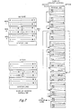
- FIG. 7 The display screen is shown divided into four regions, with the letters in each region indicating the first and last rows of characters in that particular region, for example, line B in region 1 is the first row of characters and line C represents the last row of characters in region 1. Similarly, line J represents the first row of characters in region 3 while line K represents the last row of characters.
- the "after" view of the display screen show region 3 scrolled up one row of characters, that is, row K is now the first displayed row of characters and row L is the last displayed row.
- FIGURE 7 Also shown in FIGURE 7 is a map of the RA and LA pointers showing the action of the pointers both before and after the scroll function has been completed.
- pointer LA of the status line points to row B in region 1 and pointer LA of row B points to row C. Since region 2 is a left partition split region, pointer LA of row C points to row F in region 2, while pointer RA of row C points to row J in right partition region 3. Pointer LA of row G in region 2 points to row N in region 4. Because region 3 is a right partition region, only the associated RA pointers are used to indicate the next successive row in that region. Region 3 is scrolled up by one row merely by changing pointer RA in row C of region 1 so that it points to row K in region 3 instead of row J.
- controller 16 and its associated circuitry to assign and modify the various pointers greatly reduces the processing time required to perform these functions and, since CRTC 16 operates asynchronously with CPU 10, the processing load on CPU 10 is reduced.
- Smooth scrolling i.e., the scrolling of a line one pixel or scan line at a time, may be performed independently in any of the vertical or horizontal split regions under the control of CRTC 16, which will now be described in greater detail.
- display controller CRTC 16 is a single integrated circuit device, which generates timing signals for a standard or a nonstandard raster-scan CRT monitor incorporating a non-interlaced format. CRTC 16 controls the horizontal and vertical display formatting, the independent display refresh memory 96, and the cursor address. Internal character and attribute data registers synchronize attribute and character data allowing controlled transfers between CPU 10 and display memory 96 or video attribute generator 94. As described above, controller 16 and its associated circuitry provide smoooth scrolling and split screen capabilities as well as determining the number of characters per row, the number of scan lines per row, and the number of rows per display frame. In conjunction with VAG 94, the various character attribute features are also provided.
- Controller 16 interfaces with CPU 10 through system address bus 14 (select lines A0A2), system data bus 36 (data lines D0D7), and system control bus 12 (RD/, WR/, and CE/).
- Lines AO-A2 are connected to an address decode logic circuit 112.
- Lines DO-D7 are connected to a data buffer 113 which is in turn connected to an internal data bus 114.
- the signal lines from control bus 12 are connected to an I/O control logic circuit 116.
- Address decoder 112 controls the various internal registers connected to data bus 114 by decoding the three address inputs together with the I/O control logic 116 outputs. Tables 1 and 2 below list the write and read assignments for the three select lines, AO-A2.
- I/O control 116 gates the control signals from CPU. 10 and controls data buffer 113 and the bus precharge.
- a control register 118 connected to data bus is a write-only register that contains the control bits listed in Table 3.
- Bit 0 selects either a standard or an alternate display format. The logical value of bit 0 is output as the ADF signal shown in Figure 8c.
- Bit 1 (CURON) enables the cursor output. Setting control bit 1 to zero inhibits the cursor output unconditionally.
- Bit 2 selects either a blinking or nonblinking cursor.
- Bit 3 sets the mode of operation for controller 16. Enabling the line attributes allows for a display memory format with row attributes following each row. When disabled, the display format is assumed to be conventional, that is, each row is sequentially followed by the next displayed row with no row attributes present.
- control bit 4 (COUT) appears as signal (COUT/) during a read or write to display memory 96. During active display this signal is inactive (High) and during retrace the signal is active (Low).
- Setting control bit 5 (TSTMD) reduces the display format to 16 characters per row and 2 scan lines per character row. Resetting this bit enables normal device operation. This is primarily used for testing and inspection purposes.
- a command register 120 connected to data bus 114 is an eight-bit write-only register which allows CPU 10 to issue display memory read or write commands, scroll commands, or interrupt commands.
- the register bit assignment is shown in Table 5 wherein an "x" indicates a "don't care” value.
- a character register 122 connected to data bus 114 is an eight-bit read/write register used by CPU 10 for transferring data to and from display memory 96. The lower seven bits from register 122 appear on an internal data bus 122a. Bus 122a is connected to a character data buffer 123 which is in turn connected to character data bus 92.
- An attribute register 124 is a eight-bit read/write register similar to character register 122. Register 124 is connected to an internal attribute data bus 124a which is in turn connected to an attribute data buffer 125. The eight attribute bits and the most significant character bit are connected to external attribute bus 100 as shown in Figures 1 a and 1 b.
- a cursor address register 126 connected to data bus 114 is a thirteen-bit read/write register containing the absolute display memory address of the displayable cursor. The contents of this register are also the address used for display memory transfers.
- a status register 128 connected to data bus 114 is a 6-bit read-only register with a bit assignment as shown in Table 4.
- Bit 0 indicates the start of the vertical blanking interval, i.e., the beginning of the status row.
- Bit 1 indicates that a read or write operation to display memory 96 has been completed.
- Bit 2 indicates that a smooth scroll operation has been completed. This will occur at the beginning of the status row on the last frame of the scroll.
- Bit 3 (INTP) indicates that an interrupt condition has occurred. This bit is reset or enabled by means of the command register 120.
- Bit 4 (RWBSY) is set following a read or a write command from CPU 10, indicating that the desired operation has not been completed. Upon completion of the read/write, this bit is reset.
- Bit 5 (SCRBSY) is set following a smooth scroll command from CPU 10 and is reset upon receipt of a scroll complete signal.
- a vertical split register 130 connected to data bus 114, is an 8-bit write-only register containing the column position of a vertical split and is zero based. That is, if register 130 is loaded with zero, on a split region the left partition would contain one character and the right partition would contain the remaining number of characters that are displayable.
- the overall display format is controlled by a series of cascaded free-running counters. Two independent formats are mask programmable, each having two mask programmable formats for providing separate refresh rates.
- a horizontal sync register 132 is an 8-bit counter that controls horizontal display timing and is incremented at the character rate by a CCLK signal from video attribute generator 94.
- a programmable logic array (PLA) decodes the current register value and outputs signals corresponding to the total number of displayed characters, the start of horizontal sync, the end of horizontal sync and the end of horizontal retrace which clears the register.
- PLA's are known in the art and need not be described in detail.
- a scan line/vertical adjust counter 134 is a 4-bit counter that is incremented at the end of horizontal retrace, thus counting the number of scan lines per character row. Its count is decoded by means of a PLA and when the total number of scan lines is reached it is cleared and the counter in a vertical sync register 136 is incremented. When the register 136 counter reaches its total number of character rows count, register 134 enters a vertical adjust mode which permits a resolution of the refresh rate to within one scan line. Upon completion of vertical adjust, register 134 is cleared and begins counting scan lines in the upper-most character row.
- Register 136 as described above counts character rows and is clocked by register 134.
- Register 136 is a 7-bit counter which is PLA decoded for total displayed character rows, status row position, total character rows (including vertical retrace), and vertical sync position. The vertical sync pulse is set at vertical sync position and reset on the total character rows count.
- An address counter 138 is a 4-bit counter that counts character scan lines as does register 136.
- Register 136 is used for normal characters while address counter 38 is used for double high and smooth scroll characters.
- Counter 138 tracks register 136 until one of these special character regions are detected. For double high characters counter 138 toggles between increment and inhibit increment states.
- counter 138 is preset with an offset signal from an offset counter 140 and then is incremented as before.
- Offset counter 140 is a four-bit counter which is incremented every time the status row position is reached, or once every frame. This increases the smooth scrolled offset one pixel (or scan line per region) per display frame. Offset counter 140 is initialized when a smooth scroll command is received from CPU 10 by means of command register 120.
- a blink rate register 142 is a three stage ripple counter that is clocked by the carry output of the most significant stage of offset counter 140. It is used to establish the cursor blink rate and the blink rate output.
- the display memory 96 is addressed by the thirteen bit display memory address (DMA) outputs (DMA0DMA12), from a buffer 143 connected to an internal DMA bus 143a.
- Associated control signals include write control (DMWR/), select memory or character generator (CGA), and bank select control (COUT).
- a display memory address counter 144 generates the DMA for active, or visible, display.
- Counter 144 is connected to bus 143a and contains three registers: a region 1 register 146, a region 2 register 148, and a split register 150.
- Register 146 contains the starting address of a character row and is loaded into the memory address counter 144 at the beginning of every scan line of that particular row.
- register 146 is updated with the starting address of the next row. This may be done either by: loading memory address counter 144 contents plus 1 into register 146 when scan line attributes are disabled; loading the address following the row attribute in register 146 when the link address is not valid and row attributes are enabled; or, loading the thirteen bit address stored in memory 96 at the row attribute location into register 146, when the link address is valid and row attributes are enabled.
- Region 2 register 48 is the equivalent of register 146 for a split region. That is, register 146 contains the starting address for the left region, while register 148 contains the starting address for the right region. Register 148 is loaded from either the memory address counter 144 or from display memory 96 through the internal attribute and character data buses 124a and 122a.
- Split register 150 is loaded from memory address counter 144 for a row falling into two regions with the display memory address of the row attribute of the left region. During the retrace state times, the address in register 150 is loaded into the display address counter 144 to fetch data at that location. When not on the last scan line of a split row, register 150 contains a refresh address that is loaded into memory address counter 144 following the state time throughout horizontal retrace for the purpose of refreshing dynamic memory devices.
- a read or a write to display memory command is given to the controller 16, it is synchronized in command register 120 and decoded.
- the contents of cursor address register 126 are placed onto display memory address bus 143a. If the cursor is enabled, the cursor output will be active since a cursor address register comparator 152 always compares the contents of register 126 with what is on the DMA bus 123a. In this case it is comparing the register 126 contents with itself.
- the character scan line outputs CSLO-3 from a scan line control logic circuit 154 may .also be considered to be a part of the display memory address. These outputs indicate which scan line of the character the display memory address corresponds to.
- the four bits may be either from counter 138, counter 134 or the four least significant bits of the cursor address register 126. The selection between these counters depends upon the type of row being displayed, i.e., normal, smooth scrolled, or double high. The four cursor bits are always selected during the state times and are used in accessing the external character generator RAM 106.
- a PLA follows a multiplexer in circuit 154 for the purpose of decoding the underline . position based on the selection of a standard or an alternate display format.
- a state timing logic circuit 156 is a seven bit shift register with recirculation capability. At the beginning of horizontal retrace, a one is shifted into this register and serially propagates through all stages. The outputs of the stages represent state times which are used to control a register control logic circuit 158. All row attribute fetches and display memory reads and writes occur during the state times with the row attribute fetch having priority over the command oriented memory accesses.
- the register control logic embodies control of the character 122 and attribute 124 registers with respect to the character 92 and attribute 100 external data buses.
- logic circuit 158 Also controlled by logic circuit 158 are the register transfer of memory address counter 144, the command register 120 synchronization and control logic, the precharging of character bus 122a and attribute bus 124a, and the control of buffers 123 and 125. Following the last displayed character row until the beginning of vertical adjust, the state timer recirculates shifting the "one" from the last stage back to the first, thereby increasing the bandwidth of the processor (CPU 10) access to display memory 96.
- a row attribute logic circuit 160 provides an input to the register control logic 158. based upon the row currently being displayed and the row to be displayed next.
- the outputs of the row attribute logic 160 provide forthe following: controlling counter 138 by presetting it with the offset counter 140, by clearing it, or by enabling it to count double high; signalling the register control logic 158 when a left and/or a right row attribute fetch should occur; and determining when register 146 or register 148 should be loaded from the character and attribute buses 122a, 124a.
- a set of memory control buffers 162 is connected to row attribute logic 160 and to register control logic 158 in order to buffer the inputs and outputs to display memory 96 and VAG 94.
- Table 6 summarizes the various signals and I/O ports on controller 16.
- the registers, PLA's and counters described above are known in the art and the electronics circuitry of each need not be described in detail.
- Keyboard unit 58 is self-contained, with its own microcomputer 64, for scanning and decoding the keys, assigning various functions thereto and transmitting and receiving data and instructions serially via I/F 60 to CPU 10.
- Various character formats are selectable, e.g., for different countries as stored in character RAM 106.
- the advantages of separate keyboard unit include a reduced processing load on CPU 10 and thus a faster throughput.
- keyboard unit 58 includes an array or matrix 166 of momentarily-closed single action switches arranged in rows and columns.
- Microcomputer 64 for example, a model 3870 available from MOSTEK Corporation and from Motorola, Inc., includes internal ROM and RAM. Input/ output ports, PO and P4 are connected to a series of open collector buffers U2-U4, used for strobing matrix 166. A feedback return is produced via a row path into port P5 of U1.
- Four control keys shown in the left hand portion of Figure 9, are connected to U1 through input port P1.
- Bits 5 and 6 of port PO are connected to a bidirectional data line E3 and a clock line E4 which are connected in turn to keyboard I/F 60 for serial transmission of signals thereto and therefrom.
- Lines E1 and E2 provide power and ground connections for keyboard unit 58.
- the four logic gates denoted as U5 in Figure 9 form a bell or tone circuit that is controlled by microcomputer 64 upon commands from CPU 10 and from internal error codes.
- I/F 60 converts serialized data from keyboard data 58 to a parallel form in a tri-state output shift register 168 for output onto I/O data bus 46.
- Flip-flop circuits FF1-FF4 control the data transfer to shift register 168.
- FF1 determines whether I/F 60 is in a read or a write mode and controls the data path.
- FF2 signals microcomputer 64 that CPU 10 is still processing data and is not ready to read.
- FF3 sends an interrupt signal to CPU 10 to indicate that the data in register 168 is available for reading, and FF4 establishes a time-delay to stabilize the data transfer into register 168 from the I/O data bus 46.
- the signals that appear on the left hand portion of Figure 10 are from CPU 10. This arrangement reduces the processing load on CPU 10, while expanding the versatility of keyboard unit 58.
- Figure 10a is a timing diagram showing the relationship of various signals in I/F 60 to the clock and data signals.
- the clock signal is generated by microcomputer 64, and the serial data in the read and the write modes is bi-directional.
Landscapes
- Engineering & Computer Science (AREA)
- Physics & Mathematics (AREA)
- Computer Hardware Design (AREA)
- General Physics & Mathematics (AREA)
- Theoretical Computer Science (AREA)
- Radar, Positioning & Navigation (AREA)
- Remote Sensing (AREA)
- Digital Computer Display Output (AREA)
- Controls And Circuits For Display Device (AREA)
- Document Processing Apparatus (AREA)
Description
- This invention relates generally to data display system as defined in the precharacterising part of
claim 1. - Traditional region separation has been performed using large scale computers. In such cases, data to be placed into a desired region was computed by software resident within the main computer. The data was then transmitted to a display device as a new display frame. Heretofore, data in display systems were not organized for display in terms of regions or windows into a data block. Further, the segmentation of the display into vertical and horizontal regions was performed by the large computer in software, and not at the local display device. The prior art system could not provide smooth or pixel scrolling of a vertical split region because of the immense software and processing time requirements.
- In accordance with the prior art - as disclosed in IBM Technical Disclosure Bulletin, vol. 23, No. 6, November, 1980, pages 2507-2508, H.E. Bush et al, a data display system has been advanced for forming a plurality of independently controllable display regions on a display device. This system has a data processor connected to a main memory. An input is connected to the data processor connected to the main memory display, and a data controller is connected to the data processor display memory wherein each row of characters to be displayed on the display device is assigned one or more memory location identifiers as defined by the display controller to indicate the display memory address of a subsequent row of characters to be displayed and wherein the display controller alters the sequence of rows displayed on the display device by modifying the memory location identifiers of the selected rows of characters.
- It is an object of this invention to provide a display control system which permits the smooth or discrete scrolling of a plurality of horizontal and vertical split display regions.
- Another object is to provide a system for controlling a display memory which minimizes the processing load on a system CPU.
- Still another object is to provide a system for mapping the contents of a display memory without requiring the transfer of blocks of data therein during various editing anascrórr functions.
- Yet another object is to provide a display control system which may be formatted either locally or from a remote host computer.
- Another object is to provide the system microprocessor with executable instructions at a high access rate, and to provide the microprocessor with instructions through a directly accessed memory whose capacity is less than the list of program instructions.
- In the data display system including the features of the characterising part of
claim 1, which realize the above-mentioned objects, a microprocessor controls the system operation in accordance with the list of instructions stored in a random access main memory. The main memory stores a portion of the list of instructions, while the complete list of instructions is stored in a mass data storage memory in the form of one or more GROMs. An additional ROM contains a list of instructions for initializing the system and a nonvolatile memory in the form of a CMOS RAM powered by a battery is included to store system configuration parameters in the event of a power loss. - A display device such as a CRT is controlled by a display control system formed of a CRT controller, a visual attribute generator, a display memory, and a character ROM. Alternate character sets are provided by a character RAM which is accessed by the display controller through the attribute generator. The display controller accesses the display memory asynchronously with the system microprocessor, thus decreasing the processing time and increasing the processor throughput. Segmentation of the display into multiple horizontal and vertical split regions which are independently scrollable either discretely or smoothly is provided by the linking of one or more row attribute bytes or "pointers" to each character and character attribute row stored in the display memory. In this manner, data can be manipulated on the display screen without changing the absolute address of the data in display memory. That is, only the pointers associated with each block of data (corresponding to a displayed row) needs to be modified by the display controller. Processing time is greatly reduced because whole blocks of data need not be transferred in the display memory, only the display memory addresses associated with the pointers are affected.
- For network applications, input/output means are provided for communicating with a controller or "host" computer. For local control of the system, input means in the form of a keyboard are provided. In one embodiment, the keyboard is a self-contained unit having a dedicated microcomputer. The keyboard unit communicates with the system through a keyboard interface unit that converts the serial data into a parallel form which is processed by the system microprocessor. Discrete control of the display device contrast is achieved by a contrast register in conjunction with the attribute generator.
- Other objects and many of the attendant advantages of the present invention will be readily apparent as the invention becomes better understood by reference to the following detailed description with the appended claims, when considered in conjunction with the accompanying drawings, wherein:
- Figures 1a1c form a block diagram of an electronic terminal including a display controller system according to the present invention;
- Figure 2 is a system memory map;
- Figure 3 is a diagram of the bit structure of an address byte used to access the system mass read-only program storage memory;
- Figures 4 and 5 are block diagrams of the GROM interface unit;
- Figure 6 is a pictorial representation showing the use of form descriptors and region data tables in establishing a display screen format;
- Figure 7 shows the use of display memory mapping to scroll a selected region on a display screen segmented into a plurality of regions;
- Figures 8a-8c form a block diagram of the display controller;
- Figure 9 is a schematic diagram of the self-contained keyboard unit;
- Figure 10 is a schematic diagram of the keyboard interface unit;
- Figure 10a is a timing diagram showing the relationship of the signals in the keyboard interface unit.
- Referring now to Figures 1a-1c there is shown a block diagram of an electronic input/output terminal according to the present invention. A
system microprocessor CPU 10 is coupled to asystem control bus 12 and asystem address bus 14.Control bus 12 andaddress bus 14 both extend to a countertime circuit CTC 18, a dual asynchronous transmitter/receiver DART 20, a serial input/output device SIO 22, a dynamic random-access memory (DRAM)timer 24 and a memory I/O decoder 26.System address 14 also extends to a system read-only memory (ROM) 27, aDRAM address multiplexer 28, atest ROM 29, aCMOS RAM 30, and a control I/O device 32. A battery 31 is coupled toCMOS RAM 30 to provide backup during power off conditions.CPU 10 is connected through a two-way buffer for transceiver (XCVR) 34 to asystem data bus 36.Data bus 36 extends to acontrast register 38, and to CRTC 16, CRTC 18, DART 20, and SIO 22.Data bus 36 is connected through atransceiver 40 to amemory data bus 42 which in turn extends tosystem ROM 27 and a series of DRAMs 48a-48c. Each DRAM is also connected toDRAM timer 24 and to aDRAM address bus 50 which is connected to aDRAM multiplexer 28.Data bus 36 is also connected through aXCVR 44 to an I/O data bus 46 which in turn extends totest ROM 29,CMOS RAM 30, and control I/O 32. - Program storage is provided by large scale mass read-only memory in the form of GROMs 52-1 to 52-8. The GROMs are connected to a
common GROM bus 54 which is in turn connected to I/O data bus 46 through a GROM I/F 56. - An operator interfaces with the present system by means of a
keyboard 58 which is connected to a keyboard I/F 60 through a telephonetype multiconductor cable 62. Keyboard 58 contains itsown computer 64 which permitskeyboard 58 to process instructions with a minimum computing load on .CPU 10. - A series of
test multiplexers DART 20, and channels B and A ofSIO 22, to provide loop back testing of the terminal in a local operating mode. A set ofcommunication buses O 32 and, respectively, to testmultiplexers communication buses receivers auxiliary ports AUX 2 andAUX 1. Communication with a host computer is provided by communication bus 76 which is connected through aPM interface 82 and an EIA driver-receiver 84 to an input/output port labeled HOST in the drawing. Longer distance communication is provided by means of an internal modulator-demodulator (MODEM) 85 which is also connected to communication bus 76. PM I/F 82 may be connected to a "personality module" (not shown) which permits the terminal communications to be compatible with various host computers. Abaud rate multiplexer 86 is connected to communication bus 76 and to control I/O 32 to provide synchronization and a selection of baud rates with the host computer. The timing ofbaud multiplexer 86 is provided by timer 18-0 ofCTC 18. Baud rate timing for theAUX 2 andAUX 1 ports is provided by timers 18-2 and 18-1 ofCTC 18. Timer 18-3 functions as a system timer. - A
communications option unit 87, shown by dashed lines in Figure 1c, is connected to the HOST port, thesystem address bus 14 and through an option I/F 88 to communication bus 76.Unit 87 is used to provide local and current-loop communications by methods known in the art, and need not be described in detail here. - The present terminal communicates with an operator by video display means such as a CRT (not shown) which is driven by a
controller CRTC 16. The generation of characters with various character attributes will be described in more detail below. Briefly, however, a set of characters is stored in a character ROM 90 connected toCRTC 16 by acharacter bus 92. The character, along with selected visual "attributes" generated by a videoattribute generator VAG 94 are stored inRAM display memory 96, which is connected toCRTC 16 through a register/buffer 98. In the present terminal an "attribute" is defined to mean any of the following in relation to individual characters: - high/normal intensity or background highlight, blinking, underline, reverse video, double high characters, non-display double wide characters, and double high/wide characters.
VAG 94 is connected toCRTC 16 and to displaymemory 96 by anattribute bus 100, and toCRTC 16 only through acontrol bus 102. Thedisplay memory 96 is expandable byadditional RAMS 104 connected as shown in Figure 1 a. Additional characters may be generated by including a character generator RAM 106 connected tocharacter bus 92 and toVAG 94 through a dot bus 107. The CRT intensity is controlled byprogrammable contrast register 38 through avideo amplifier 108, which is also connected toVAG 94. - Referring now to Figure 2, there is shown a memory map of the present system illustrating the assigned memory of the various memory devices in hexadecimal form. In the basic 8-bit bytes in memory locations 0000-7FFF, and is expandable to 64K bytes in memory locations 8000-FFFF by the addition of
DRAMs 48b and 48c. - Memory locations 0000-1FFF are assigned to
system ROM 27, which contains 2K bytes (expandable to 8K) of program instructions to control the system initialization and diagnostics on power up, as well as instructions for loading DRAM 48a from the program storage memory resident in the GROMs. DRAM 48a is used byCPU 10 for execution of instructions to control the terminal. - Locations 2000-3000 are assigned to test ROM 29 (48K byte maximum) which is used primarily during manufacture for test and diagnostic aids such as signature analysis.
-
Address 3000 is a write-only memory location that stores data incontrast register 38 to control the intensity level of the CRT as set by the operator. The attributes video on/off, background select, and highlight select are also controlled byregister 38. - A read at memory location 3A00 inputs the data sent by
keyboard 58 and resets its associated interrupt. A write to this location sends data to the keyboard for processing. - Read and write commands to memory locations 3A80-3A87 communicate the terminal configuration from control I/
O 32 toCPU 10, that is, which of the basic and expandable devices are installed, as well as configuring the operational mode of the various communication devices are selected by the operator. Location 3BOO is reserved forcommunication option unit 87, which functions as described above. - Locations 3E00-3EFF are assigned to the 256
byte CMOS RAM 30, which is powered by a battery 31 to preserve its contents during power off conditions.CMOS RAM 30 stores terminal configuration information such as communications baud rates so that the terminal can readily communicate with the host computer when power is restored. -
Display memory 96, which stores characters and associated attributes for display on the CRT screen, is accessed throughCRT controller 16 as an I/O device.Display memory 96 contains 2K 16-bit bytes and is expandable to 8K in 2K increments. - The GROM storage memory is accessed by addressing the GROM I/
F 56 at memory location 3B80. A read from thislocation inputs 4 bits of data from the selected GROM, and a write to this memory location outputs address and control information for accessing the GROM. In the basic terminal configuration three 16K byte GROMs, 52-1, 52-2, and 52-3, form a 48K byte program storage memory. This is expandable to a total of 128K bytes in 16K increments by the addition of GROMs 52-4 to 52-8. Dashed line 110 in Figure 1a denotes the expanded portions of the operating and program storage memory. Basically, a GROM is a PMOS, metal gate read-only memory that provides low cost mass data storage. In the present terminal, program instructions are down-loaded from the GROM to the DRAM operating system memory as needed for execution by CPU10. In this manner, a 16K DRAM can be used for execution of 48K of program instruction. A similar method of overlaying program instructions into the DRAM is described in a co-pending patent application with publ. Nr. EP-A-48816 by Skelton, et al entitled "Virtual Memory Microcomputer Architecture." - Referring now to Figures 3-5, the GROM accessing procedure is shown in greater detail. Figure 3 shows the bit structure of a 20-bit byte used to access the GROM. The byte is loaded into GROM I/
F 56 in 4- bit blocks or "nibbles" N1-N5. Bits 0-13 are used to select any one of 16K byte addresses in a particular GROM, while bits 14-17 are used to select one of up to eight GROMS. One embodiment of the GROM I/F is shown in Figure 4 and 5, illustrating circuitry for accessing a 16K byte GROM through a 4 bit data/address line DO-D3. - The display control system of the present terminal is formed of
CRT controller 16,video attribute generator 94,display memory 96, character ROM 90,contrast register 38 and the associated circuitry andexpandable memories 104 and 106. Briefly,CRTC 16 provides horizontal and vertical timing for the CRT, addressesdisplay memory 96 for CRT refresh, provides the scan line addresses for character ROM 90 and character generator 106, controls the cursor on the CRT, controls data transfers betweenCPU 10 anddisplay memory 96 or character generator 106, and controls videoattribute generator VAG 94.VAG 94 converts parallel dot data into serial video data, modifies dot data according to attributes and control inputs, generates a character clock from a video dot clock, and provides a data path for character generator access. The CRT is configured to display information in a 25 row by 80 or 132 column format, with theline 25 reserved for terminal status messages. Each character cell defined by a row/column address is 9 x 11 dots or pixels, with a character size of 7 x 9 pixels. - The present terminal, as configured by either the operator or the host computer, allows for dividing the display memory into partitions. Each partition is called an editing boundary. The partition is defined in terms of rows of display, each row having 80 or 132 columns of display information. Additionally, the editing boundary may be defined to be an unformatted display containing no fields, but containing display attributes on a character-by-character basis. The formatted display, called a FORM, contains at least one field and may contain display attributes on a character-by-character basis.
- Only one editing boundary is displayed at a time. If more than one editing boundary is resident in the terminal, the length of each editing boundary must be equal to or greater than 24 rows of display information. That is, if 12 rows of double high/wide characters are used, then the 12 rows of double high/ wide characters are 24 rows of display information.
- A formatted editing boundary consists of "regions." A region is defined as a consecutive number of display rows viewed by the operator. The maximum number of consecutive rows possible for a region is.24 and the minimum is 1. However, the region data may exceed the display rows allocated for the defined region. This is called a scrolled region. Additionally, a region is defined as a full partition, left partition, or right partition. A full partition region is a region displayed to the operator using all columns possible in the CRT display. A left partition region is a region displayed to the operator using all columns to the left of the vertical split defined by the FORM. A right partition is a region displayed to the operator using all columns from and including the vertical split to the right defined by the FORM. If a region is defined as display only, with no operator access to the region, an entire region may be defined as a "protected region." A protected region is always guarded for transmission. A vertical split may exist for any FORM, however, only one vertical split may exist for any one form. A vertical split is a selected column 1-80 or 1-132 which defines the starting column of any right partition region.
- Each region is a "window." A window which shows all the data in the display at once is called a fixed region or a non-scrollable region. A window that shows only a part or a segment of the data assigned to the window is called a scrolled. region. Every editing boundary contains at least one window. The window may consist of all of the editing boundary which in turn may consist of all terminal memory, butthe window still exists. Each region can be individually scrolled either discreetly or smoothly. Thus, in effect, each region can function as an independent display.
- These and other features are obtained by means of a "data-linking" procedure whereby two "line attributes" are generated and stored in
display memory 96 for each row of characters and character attributes on the CRT screen. A line attribute is a byte of data which functions as a pointer, telling CRT ·controller 16 at which display memory location the first character in the next row of characters appears. In the case of a vertical split region, wherein a full partition region is followed by a left and a right partition region on the display, the last character of the last row of the full partition region will be followed in display memory by a right attribute (RA) and a left attribute (LA). The LA points to the display memory location of the first character in the first row in the left partition, and the RA points to the memory location of the first character in the first row of the right partition. In this manner, various display functions such as inserting/ deleting lines and scrolling are achieved by merely modifying the pointers RA and LA to indicate the memory location of the next desired row of characters. This greatly increases the processing throughput ofCPU 10 because only the affected pointers need to be modified, without rearranging character and character attribute data in the display memory. - By way of example, and to aid in the understanding of the form and region concept described above, reference is made to Figure 6 wherein the display screen as seen by an operator is partitioned into four regions. It is assumed for this example that the terminal has been configured by the host computer to define two editing boundaries or forms. The form descriptors as well as region data tables (RDT) are loaded into the terminal memory or DRAM. Form
descriptor 2 contains the information for configuring the display screen as shown in the drawing, that is, there is a vertical split atcolumn 40 of the display screen and the form starts atdisplay memory location 10 and ends atdisplay memory location 50. As shown in the display memory map each of the four regions is a scrollable region, that is, the number of rows in each region exceeds the available "window" for display. Since the terminal in this example is configured to have a two page display memory, there are 48 lines of information available for the region definitions, although only 24 lines may be displayed at one time.Form 2 has four associated region data tables (RDT), one for each region on the display screen. Each RDT contains 8 bytes of information.Byte 0 is a predetermined region number, for example, to indicate whether a left or a right partition region will be displayed on the screen.Byte 1 indicates the starting row on the display screen for the associated region.Byte 2 is the current memory display starting row, that is, the display memory address of the currently displayed row.Byte 3 indicates the memory starting row number in the region, andbyte 4 is the display ending row.Byte 5 is the current memory display ending row,byte 6 is the region memory ending row number in display memory, andbyte 7 is the maximum relative column number for the region on the display screen. For example, referring to the RDT forregion 1 in Figure 6,region 1 character and character attribute data are stored in display memory locations 10-24. The currently displayed information fromregion 1 on the display screen, however, is formed of 8 lines that are stored in display memory locations 12-19, and appear on the display screen rows 0-7. That is, memory locations 12-19 comprise the "window" ofregion 1 that is currently displayed. Sinceregion 2 is a right partition split region occupying the same display screen rows asregion 1, the display window forregion 2 is the same size as the window forregion 1. It should be noted that 48 rows of display memory have been used forform 2, although only 24 rows of information appear on the display screen at a time.Regions - Although in Figure 6 the rows of information in display memory corresponding to the rows on the display screen are shown in sequential order, they may in fact be located at any display memory location. The RA and LA pointers associated with each row of screen information, as described above, will map the location of the next characters in display memory to be displayed on the screen.
- Referring now to Figure 7, the use of these pointers in scrolling and individual region on the display screen will now be described by way of example. The display screen is shown divided into four regions, with the letters in each region indicating the first and last rows of characters in that particular region, for example, line B in
region 1 is the first row of characters and line C represents the last row of characters inregion 1. Similarly, line J represents the first row of characters inregion 3 while line K represents the last row of characters. The "after" view of the displayscreen show region 3 scrolled up one row of characters, that is, row K is now the first displayed row of characters and row L is the last displayed row. Also shown in FIGURE 7 is a map of the RA and LA pointers showing the action of the pointers both before and after the scroll function has been completed. Before scrolling is initiated pointer LA of the status line points to row B inregion 1 and pointer LA of row B points to row C. Sinceregion 2 is a left partition split region, pointer LA of row C points to row F inregion 2, while pointer RA of row C points to row J inright partition region 3. Pointer LA of row G inregion 2 points to row N inregion 4. Becauseregion 3 is a right partition region, only the associated RA pointers are used to indicate the next successive row in that region.Region 3 is scrolled up by one row merely by changing pointer RA in row C ofregion 1 so that it points to row K inregion 3 instead of row J. Thus, scrolling and other editing functions are achieved by changing the pointers only, rather than rearranging whole blocks of data in display memory as was done in prior art systems. Further, the use ofcontroller 16 and its associated circuitry to assign and modify the various pointers greatly reduces the processing time required to perform these functions and, sinceCRTC 16 operates asynchronously withCPU 10, the processing load onCPU 10 is reduced. - Smooth scrolling, i.e., the scrolling of a line one pixel or scan line at a time, may be performed independently in any of the vertical or horizontal split regions under the control of
CRTC 16, which will now be described in greater detail.


- In one embodiment,
display controller CRTC 16 is a single integrated circuit device, which generates timing signals for a standard or a nonstandard raster-scan CRT monitor incorporating a non-interlaced format.CRTC 16 controls the horizontal and vertical display formatting, the independentdisplay refresh memory 96, and the cursor address. Internal character and attribute data registers synchronize attribute and character data allowing controlled transfers betweenCPU 10 anddisplay memory 96 orvideo attribute generator 94. As described above,controller 16 and its associated circuitry provide smoooth scrolling and split screen capabilities as well as determining the number of characters per row, the number of scan lines per row, and the number of rows per display frame. In conjunction withVAG 94, the various character attribute features are also provided. - Referring now to Figures 8a-8c,
CRTC 16 is shown in block diagram form.Controller 16 interfaces withCPU 10 through system address bus 14 (select lines A0A2), system data bus 36 (data lines D0D7), and system control bus 12 (RD/, WR/, and CE/). Lines AO-A2 are connected to an addressdecode logic circuit 112. Lines DO-D7 are connected to adata buffer 113 which is in turn connected to aninternal data bus 114. The signal lines fromcontrol bus 12 are connected to an I/Ocontrol logic circuit 116.Address decoder 112 controls the various internal registers connected todata bus 114 by decoding the three address inputs together with the I/O control logic 116 outputs. Tables 1 and 2 below list the write and read assignments for the three select lines, AO-A2. I/O control 116 gates the control signals from CPU. 10 andcontrols data buffer 113 and the bus precharge. - A
control register 118 connected to data bus is a write-only register that contains the control bits listed in Table 3. Bit 0 (DFMS) selects either a standard or an alternate display format. The logical value ofbit 0 is output as the ADF signal shown in Figure 8c. Bit 1 (CURON) enables the cursor output. Settingcontrol bit 1 to zero inhibits the cursor output unconditionally. Bit 2 (CBLINK) selects either a blinking or nonblinking cursor. Bit 3 (ENLA) sets the mode of operation forcontroller 16. Enabling the line attributes allows for a display memory format with row attributes following each row. When disabled, the display format is assumed to be conventional, that is, each row is sequentially followed by the next displayed row with no row attributes present. The logical value of control bit 4 (COUT) appears as signal (COUT/) during a read or write to displaymemory 96. During active display this signal is inactive (High) and during retrace the signal is active (Low). Setting control bit 5 (TSTMD) reduces the display format to 16 characters per row and 2 scan lines per character row. Resetting this bit enables normal device operation. This is primarily used for testing and inspection purposes. - A
command register 120 connected todata bus 114 is an eight-bit write-only register which allowsCPU 10 to issue display memory read or write commands, scroll commands, or interrupt commands. The register bit assignment is shown in Table 5 wherein an "x" indicates a "don't care" value. - A
character register 122 connected todata bus 114 is an eight-bit read/write register used byCPU 10 for transferring data to and fromdisplay memory 96. The lower seven bits fromregister 122 appear on an internal data bus 122a. Bus 122a is connected to acharacter data buffer 123 which is in turn connected tocharacter data bus 92. Anattribute register 124 is a eight-bit read/write register similar to character register 122.Register 124 is connected to an internal attribute data bus 124a which is in turn connected to anattribute data buffer 125. The eight attribute bits and the most significant character bit are connected toexternal attribute bus 100 as shown in Figures 1 a and 1 b. Acursor address register 126 connected todata bus 114 is a thirteen-bit read/write register containing the absolute display memory address of the displayable cursor. The contents of this register are also the address used for display memory transfers. - A
status register 128 connected todata bus 114 is a 6-bit read-only register with a bit assignment as shown in Table 4. Bit 0 (SVBLK) indicates the start of the vertical blanking interval, i.e., the beginning of the status row. Bit 1 (RWCOM) indicates that a read or write operation to displaymemory 96 has been completed. Bit 2 (SCRCOM) indicates that a smooth scroll operation has been completed. This will occur at the beginning of the status row on the last frame of the scroll. Bit 3 (INTP) indicates that an interrupt condition has occurred. This bit is reset or enabled by means of thecommand register 120. Bit 4 (RWBSY) is set following a read or a write command fromCPU 10, indicating that the desired operation has not been completed. Upon completion of the read/write, this bit is reset. Bit 5 (SCRBSY) is set following a smooth scroll command fromCPU 10 and is reset upon receipt of a scroll complete signal.

- A
vertical split register 130, connected todata bus 114, is an 8-bit write-only register containing the column position of a vertical split and is zero based. That is, ifregister 130 is loaded with zero, on a split region the left partition would contain one character and the right partition would contain the remaining number of characters that are displayable. - The overall display format is controlled by a series of cascaded free-running counters. Two independent formats are mask programmable, each having two mask programmable formats for providing separate refresh rates. A
horizontal sync register 132 is an 8-bit counter that controls horizontal display timing and is incremented at the character rate by a CCLK signal fromvideo attribute generator 94. A programmable logic array (PLA) decodes the current register value and outputs signals corresponding to the total number of displayed characters, the start of horizontal sync, the end of horizontal sync and the end of horizontal retrace which clears the register. The operation of PLA's are known in the art and need not be described in detail. A scan line/vertical adjust counter 134 is a 4-bit counter that is incremented at the end of horizontal retrace, thus counting the number of scan lines per character row. Its count is decoded by means of a PLA and when the total number of scan lines is reached it is cleared and the counter in avertical sync register 136 is incremented. When theregister 136 counter reaches its total number of character rows count, register 134 enters a vertical adjust mode which permits a resolution of the refresh rate to within one scan line. Upon completion of vertical adjust, register 134 is cleared and begins counting scan lines in the upper-most character row. - Vertical sync register 136 as described above counts character rows and is clocked by register 134.
Register 136 is a 7-bit counter which is PLA decoded for total displayed character rows, status row position, total character rows (including vertical retrace), and vertical sync position. The vertical sync pulse is set at vertical sync position and reset on the total character rows count. - An
address counter 138 is a 4-bit counter that counts character scan lines as does register 136.Register 136 is used for normal characters whileaddress counter 38 is used for double high and smooth scroll characters. Counter 138 tracks register 136 until one of these special character regions are detected. For double high characters counter 138 toggles between increment and inhibit increment states. For the scrolling function,counter 138 is preset with an offset signal from an offsetcounter 140 and then is incremented as before. Offset counter 140 is a four-bit counter which is incremented every time the status row position is reached, or once every frame. This increases the smooth scrolled offset one pixel (or scan line per region) per display frame. Offset counter 140 is initialized when a smooth scroll command is received fromCPU 10 by means ofcommand register 120. This either presets or clears counter 140 based upon the direction of the scroll. Ablink rate register 142 is a three stage ripple counter that is clocked by the carry output of the most significant stage of offsetcounter 140. It is used to establish the cursor blink rate and the blink rate output. - The
display memory 96 is addressed by the thirteen bit display memory address (DMA) outputs (DMA0DMA12), from abuffer 143 connected to an internal DMA bus 143a. Associated control signals include write control (DMWR/), select memory or character generator (CGA), and bank select control (COUT). A displaymemory address counter 144 generates the DMA for active, or visible, display.Counter 144 is connected to bus 143a and contains three registers: aregion 1register 146, aregion 2register 148, and asplit register 150.Register 146 contains the starting address of a character row and is loaded into thememory address counter 144 at the beginning of every scan line of that particular row. After the last scan line of a row has been displayed, register 146 is updated with the starting address of the next row. This may be done either by: loadingmemory address counter 144 contents plus 1 intoregister 146 when scan line attributes are disabled; loading the address following the row attribute inregister 146 when the link address is not valid and row attributes are enabled; or, loading the thirteen bit address stored inmemory 96 at the row attribute location intoregister 146, when the link address is valid and row attributes are enabled. -
Region 2 register 48 is the equivalent ofregister 146 for a split region. That is, register 146 contains the starting address for the left region, whileregister 148 contains the starting address for the right region.Register 148 is loaded from either thememory address counter 144 or fromdisplay memory 96 through the internal attribute and character data buses 124a and 122a. -
Split register 150 is loaded frommemory address counter 144 for a row falling into two regions with the display memory address of the row attribute of the left region. During the retrace state times, the address inregister 150 is loaded into thedisplay address counter 144 to fetch data at that location. When not on the last scan line of a split row, register 150 contains a refresh address that is loaded intomemory address counter 144 following the state time throughout horizontal retrace for the purpose of refreshing dynamic memory devices. When a read or a write to display memory command is given to thecontroller 16, it is synchronized incommand register 120 and decoded. During the actual read or write operation, which occurs during the state time of retrace, the contents ofcursor address register 126 are placed onto display memory address bus 143a. If the cursor is enabled, the cursor output will be active since a cursoraddress register comparator 152 always compares the contents ofregister 126 with what is on the DMA bus 123a. In this case it is comparing theregister 126 contents with itself. - The character scan line outputs CSLO-3 from a scan line
control logic circuit 154 may .also be considered to be a part of the display memory address. These outputs indicate which scan line of the character the display memory address corresponds to. The four bits may be either fromcounter 138, counter 134 or the four least significant bits of thecursor address register 126. The selection between these counters depends upon the type of row being displayed, i.e., normal, smooth scrolled, or double high. The four cursor bits are always selected during the state times and are used in accessing the external character generator RAM 106. A PLA follows a multiplexer incircuit 154 for the purpose of decoding the underline . position based on the selection of a standard or an alternate display format. - A state
timing logic circuit 156 is a seven bit shift register with recirculation capability. At the beginning of horizontal retrace, a one is shifted into this register and serially propagates through all stages. The outputs of the stages represent state times which are used to control a registercontrol logic circuit 158. All row attribute fetches and display memory reads and writes occur during the state times with the row attribute fetch having priority over the command oriented memory accesses. The register control logic embodies control of thecharacter 122 and attribute 124 registers with respect to thecharacter 92 andattribute 100 external data buses. Also controlled bylogic circuit 158 are the register transfer ofmemory address counter 144, thecommand register 120 synchronization and control logic, the precharging of character bus 122a and attribute bus 124a, and the control ofbuffers memory 96. - A row
attribute logic circuit 160 provides an input to theregister control logic 158. based upon the row currently being displayed and the row to be displayed next. The outputs of therow attribute logic 160 provide forthe following: controlling counter 138 by presetting it with the offsetcounter 140, by clearing it, or by enabling it to count double high; signalling theregister control logic 158 when a left and/or a right row attribute fetch should occur; and determining whenregister 146 or register 148 should be loaded from the character and attribute buses 122a, 124a. A set of memory control buffers 162 is connected to rowattribute logic 160 and to registercontrol logic 158 in order to buffer the inputs and outputs to displaymemory 96 andVAG 94. - Table 6 below summarizes the various signals and I/O ports on
controller 16. The registers, PLA's and counters described above are known in the art and the electronics circuitry of each need not be described in detail.

-
Keyboard unit 58 is self-contained, with itsown microcomputer 64, for scanning and decoding the keys, assigning various functions thereto and transmitting and receiving data and instructions serially via I/F 60 toCPU 10. Various character formats are selectable, e.g., for different countries as stored in character RAM 106. The advantages of separate keyboard unit include a reduced processing load onCPU 10 and thus a faster throughput. - Referring now to Figure 9,
keyboard unit 58 includes an array ormatrix 166 of momentarily-closed single action switches arranged in rows and columns.Microcomputer 64, for example, a model 3870 available from MOSTEK Corporation and from Motorola, Inc., includes internal ROM and RAM. Input/ output ports, PO and P4 are connected to a series of open collector buffers U2-U4, used forstrobing matrix 166. A feedback return is produced via a row path into port P5 of U1. Four control keys, shown in the left hand portion of Figure 9, are connected to U1 through input port P1.Bits F 60 for serial transmission of signals thereto and therefrom. Lines E1 and E2 provide power and ground connections forkeyboard unit 58. The four logic gates denoted as U5 in Figure 9 form a bell or tone circuit that is controlled bymicrocomputer 64 upon commands fromCPU 10 and from internal error codes. - Referring now to Figure 10, I/
F 60 converts serialized data fromkeyboard data 58 to a parallel form in a tri-stateoutput shift register 168 for output onto I/O data bus 46. Flip-flop circuits FF1-FF4 control the data transfer to shiftregister 168. FF1 determines whether I/F 60 is in a read or a write mode and controls the data path. FF2 signalsmicrocomputer 64 thatCPU 10 is still processing data and is not ready to read. FF3 sends an interrupt signal toCPU 10 to indicate that the data inregister 168 is available for reading, and FF4 establishes a time-delay to stabilize the data transfer intoregister 168 from the I/O data bus 46. The signals that appear on the left hand portion of Figure 10 are fromCPU 10. This arrangement reduces the processing load onCPU 10, while expanding the versatility ofkeyboard unit 58. - Figure 10a is a timing diagram showing the relationship of various signals in I/
F 60 to the clock and data signals. The clock signal is generated bymicrocomputer 64, and the serial data in the read and the write modes is bi-directional.
Claims (3)
Applications Claiming Priority (4)
| Application Number | Priority Date | Filing Date | Title |
|---|---|---|---|
| US237318 | 1981-02-23 | ||
| US237316 | 1981-02-23 | ||
| US06/237,318 US4386410A (en) | 1981-02-23 | 1981-02-23 | Display controller for multiple scrolling regions |
| US06/237,316 US4412294A (en) | 1981-02-23 | 1981-02-23 | Display system with multiple scrolling regions |
Publications (3)
| Publication Number | Publication Date |
|---|---|
| EP0059349A2 EP0059349A2 (en) | 1982-09-08 |
| EP0059349A3 EP0059349A3 (en) | 1982-10-13 |
| EP0059349B1 true EP0059349B1 (en) | 1986-08-06 |
Family
ID=26930555
Family Applications (1)
| Application Number | Title | Priority Date | Filing Date |
|---|---|---|---|
| EP19820101013 Expired EP0059349B1 (en) | 1981-02-23 | 1982-02-11 | Display system with multiple scrolling regions |
Country Status (3)
| Country | Link |
|---|---|
| EP (1) | EP0059349B1 (en) |
| JP (2) | JPH0740179B2 (en) |
| DE (1) | DE3272407D1 (en) |
Families Citing this family (14)
| Publication number | Priority date | Publication date | Assignee | Title |
|---|---|---|---|---|
| JPS59105683A (en) * | 1982-12-10 | 1984-06-19 | 株式会社日立製作所 | Display controller |
| JPH079569B2 (en) * | 1983-07-01 | 1995-02-01 | 株式会社日立製作所 | Display controller and graphic display device using the same |
| FI842153A (en) * | 1983-06-13 | 1984-12-14 | Honeywell Inf Systems | VARIABELT BELASTBAR TECKENGENERATOR. |
| IT1162945B (en) * | 1983-09-30 | 1987-04-01 | Olivetti & Co Spa | EQUIPMENT FOR THE VISUALIZATION OF IMAGES DEFINED BY A MULTIPLE OF DATA LINES |
| US4611202A (en) * | 1983-10-18 | 1986-09-09 | Digital Equipment Corporation | Split screen smooth scrolling arrangement |
| US4714918A (en) * | 1984-04-30 | 1987-12-22 | International Business Machines Corporation | Window view control |
| FR2566949B1 (en) * | 1984-06-29 | 1986-12-26 | Texas Instruments France | SYSTEM FOR DISPLAYING VIDEO IMAGES ON A LINE-BY-LINE AND POINT-BY-POINT SCANNING SCREEN |
| JPS6194087A (en) * | 1984-10-15 | 1986-05-12 | 松下電器産業株式会社 | Display controller |
| JPS61151691A (en) * | 1984-12-20 | 1986-07-10 | インタ−ナショナル ビジネス マシ−ンズ コ−ポレ−ション | Display unit |
| CA1233257A (en) * | 1984-12-26 | 1988-02-23 | Irene H. Hernandez | Tailored document building |
| US4663615A (en) * | 1984-12-26 | 1987-05-05 | International Business Machines Corporation | Document creation |
| GB2176979A (en) * | 1985-06-06 | 1987-01-07 | Aston Electronic Designs Ltd | Video signal manipulation system |
| US4769637A (en) * | 1985-11-26 | 1988-09-06 | Digital Equipment Corporation | Video display control circuit arrangement |
| JP2002149391A (en) * | 2000-09-01 | 2002-05-24 | Sony Corp | Device and method for reproduction |
Family Cites Families (6)
| Publication number | Priority date | Publication date | Assignee | Title |
|---|---|---|---|---|
| US4075620A (en) * | 1976-04-29 | 1978-02-21 | Gte Sylvania Incorporated | Video display system |
| US4126814A (en) * | 1976-12-09 | 1978-11-21 | Rca Corporation | Electron gun control system |
| JPS5390820A (en) * | 1977-01-21 | 1978-08-10 | Toshiba Corp | Roll-up system for display unit |
| JPS5444442A (en) * | 1977-09-14 | 1979-04-07 | Nec Corp | Character display system |
| GB1572318A (en) * | 1978-03-31 | 1980-07-30 | Ibm | Display system |
| JPS55115140A (en) * | 1979-02-27 | 1980-09-04 | Hitachi Ltd | Display unit |
-
1982
- 1982-02-11 DE DE8282101013T patent/DE3272407D1/en not_active Expired
- 1982-02-11 EP EP19820101013 patent/EP0059349B1/en not_active Expired
- 1982-02-22 JP JP57027263A patent/JPH0740179B2/en not_active Expired - Lifetime
-
1991
- 1991-08-14 JP JP3204318A patent/JP2697800B2/en not_active Expired - Lifetime
Also Published As
| Publication number | Publication date |
|---|---|
| JPH05134652A (en) | 1993-05-28 |
| JPH0740179B2 (en) | 1995-05-01 |
| EP0059349A3 (en) | 1982-10-13 |
| EP0059349A2 (en) | 1982-09-08 |
| JPS57158878A (en) | 1982-09-30 |
| JP2697800B2 (en) | 1998-01-14 |
| DE3272407D1 (en) | 1986-09-11 |
Similar Documents
| Publication | Publication Date | Title |
|---|---|---|
| US4412294A (en) | Display system with multiple scrolling regions | |
| US4386410A (en) | Display controller for multiple scrolling regions | |
| US4404554A (en) | Video address generator and timer for creating a flexible CRT display | |
| EP0059349B1 (en) | Display system with multiple scrolling regions | |
| US4104624A (en) | Microprocessor controlled CRT display system | |
| US5345552A (en) | Control for computer windowing display | |
| US4642794A (en) | Video update FIFO buffer | |
| EP0153197B1 (en) | A method of operating a display system | |
| US4249172A (en) | Row address linking control system for video display terminal | |
| US4642789A (en) | Video memory controller | |
| EP0279229A2 (en) | A graphics display system | |
| US4117469A (en) | Computer assisted display processor having memory sharing by the computer and the processor | |
| JPH0469794B2 (en) | ||
| US4418343A (en) | CRT Refresh memory system | |
| EP0279225B1 (en) | Reconfigurable counters for addressing in graphics display systems | |
| US4620186A (en) | Multi-bit write feature for video RAM | |
| EP0215984B1 (en) | Graphic display apparatus with combined bit buffer and character graphics store | |
| US4119953A (en) | Timesharing programmable display system | |
| JPH1091136A (en) | Electronic computer | |
| JPS6330632B2 (en) | ||
| US4803478A (en) | Horizontal scroll method and apparatus | |
| EP0752694B1 (en) | Method for quickly painting and copying shallow pixels on a deep frame buffer | |
| CA1162319A (en) | Video processor and controller | |
| US4398190A (en) | Character generator display system | |
| EP0422300B1 (en) | Display system with graphics cursor |
Legal Events
| Date | Code | Title | Description |
|---|---|---|---|
| PUAI | Public reference made under article 153(3) epc to a published international application that has entered the european phase |
Free format text: ORIGINAL CODE: 0009012 |
|
| PUAL | Search report despatched |
Free format text: ORIGINAL CODE: 0009013 |
|
| AK | Designated contracting states |
Designated state(s): DE FR GB NL |
|
| AK | Designated contracting states |
Designated state(s): DE FR GB NL |
|
| 17P | Request for examination filed |
Effective date: 19830328 |
|
| GRAA | (expected) grant |
Free format text: ORIGINAL CODE: 0009210 |
|
| AK | Designated contracting states |
Kind code of ref document: B1 Designated state(s): DE FR GB NL |
|
| REF | Corresponds to: |
Ref document number: 3272407 Country of ref document: DE Date of ref document: 19860911 |
|
| ET | Fr: translation filed | ||
| PLBE | No opposition filed within time limit |
Free format text: ORIGINAL CODE: 0009261 |
|
| STAA | Information on the status of an ep patent application or granted ep patent |
Free format text: STATUS: NO OPPOSITION FILED WITHIN TIME LIMIT |
|
| 26N | No opposition filed | ||
| PGFP | Annual fee paid to national office [announced via postgrant information from national office to epo] |
Ref country code: GB Payment date: 20010104 Year of fee payment: 20 |
|
| PGFP | Annual fee paid to national office [announced via postgrant information from national office to epo] |
Ref country code: FR Payment date: 20010201 Year of fee payment: 20 |
|
| PGFP | Annual fee paid to national office [announced via postgrant information from national office to epo] |
Ref country code: DE Payment date: 20010228 Year of fee payment: 20 |
|
| PGFP | Annual fee paid to national office [announced via postgrant information from national office to epo] |
Ref country code: NL Payment date: 20010319 Year of fee payment: 20 |
|
| REG | Reference to a national code |
Ref country code: GB Ref legal event code: IF02 |
|
| PG25 | Lapsed in a contracting state [announced via postgrant information from national office to epo] |
Ref country code: GB Free format text: LAPSE BECAUSE OF EXPIRATION OF PROTECTION Effective date: 20020210 |
|
| PG25 | Lapsed in a contracting state [announced via postgrant information from national office to epo] |
Ref country code: NL Free format text: LAPSE BECAUSE OF EXPIRATION OF PROTECTION Effective date: 20020211 |
|
| REG | Reference to a national code |
Ref country code: GB Ref legal event code: PE20 Effective date: 20020210 |
|
| NLV7 | Nl: ceased due to reaching the maximum lifetime of a patent |