EP0069854A2 - Method of forming via holes in insulating layers - Google Patents
Method of forming via holes in insulating layers Download PDFInfo
- Publication number
- EP0069854A2 EP0069854A2 EP82104711A EP82104711A EP0069854A2 EP 0069854 A2 EP0069854 A2 EP 0069854A2 EP 82104711 A EP82104711 A EP 82104711A EP 82104711 A EP82104711 A EP 82104711A EP 0069854 A2 EP0069854 A2 EP 0069854A2
- Authority
- EP
- European Patent Office
- Prior art keywords
- resist
- layer
- minutes
- substrate
- openings
- Prior art date
- Legal status (The legal status is an assumption and is not a legal conclusion. Google has not performed a legal analysis and makes no representation as to the accuracy of the status listed.)
- Granted
Links
Images

Classifications
-
- G—PHYSICS
- G03—PHOTOGRAPHY; CINEMATOGRAPHY; ANALOGOUS TECHNIQUES USING WAVES OTHER THAN OPTICAL WAVES; ELECTROGRAPHY; HOLOGRAPHY
- G03F—PHOTOMECHANICAL PRODUCTION OF TEXTURED OR PATTERNED SURFACES, e.g. FOR PRINTING, FOR PROCESSING OF SEMICONDUCTOR DEVICES; MATERIALS THEREFOR; ORIGINALS THEREFOR; APPARATUS SPECIALLY ADAPTED THEREFOR
- G03F7/00—Photomechanical, e.g. photolithographic, production of textured or patterned surfaces, e.g. printing surfaces; Materials therefor, e.g. comprising photoresists; Apparatus specially adapted therefor
- G03F7/26—Processing photosensitive materials; Apparatus therefor
- G03F7/40—Treatment after imagewise removal, e.g. baking
-
- G—PHYSICS
- G03—PHOTOGRAPHY; CINEMATOGRAPHY; ANALOGOUS TECHNIQUES USING WAVES OTHER THAN OPTICAL WAVES; ELECTROGRAPHY; HOLOGRAPHY
- G03F—PHOTOMECHANICAL PRODUCTION OF TEXTURED OR PATTERNED SURFACES, e.g. FOR PRINTING, FOR PROCESSING OF SEMICONDUCTOR DEVICES; MATERIALS THEREFOR; ORIGINALS THEREFOR; APPARATUS SPECIALLY ADAPTED THEREFOR
- G03F7/00—Photomechanical, e.g. photolithographic, production of textured or patterned surfaces, e.g. printing surfaces; Materials therefor, e.g. comprising photoresists; Apparatus specially adapted therefor
- G03F7/004—Photosensitive materials
- G03F7/09—Photosensitive materials characterised by structural details, e.g. supports, auxiliary layers
- G03F7/094—Multilayer resist systems, e.g. planarising layers
-
- G—PHYSICS
- G03—PHOTOGRAPHY; CINEMATOGRAPHY; ANALOGOUS TECHNIQUES USING WAVES OTHER THAN OPTICAL WAVES; ELECTROGRAPHY; HOLOGRAPHY
- G03F—PHOTOMECHANICAL PRODUCTION OF TEXTURED OR PATTERNED SURFACES, e.g. FOR PRINTING, FOR PROCESSING OF SEMICONDUCTOR DEVICES; MATERIALS THEREFOR; ORIGINALS THEREFOR; APPARATUS SPECIALLY ADAPTED THEREFOR
- G03F7/00—Photomechanical, e.g. photolithographic, production of textured or patterned surfaces, e.g. printing surfaces; Materials therefor, e.g. comprising photoresists; Apparatus specially adapted therefor
- G03F7/26—Processing photosensitive materials; Apparatus therefor
- G03F7/30—Imagewise removal using liquid means
Definitions
- This invention relates to the formation of a pattern of openings in a layer of a positive resist system on semiconductor devices using high energy electron beam radiation, and more particularly to the development of said exposed resist layer with horizontal and vertical control of the hole dimensions. Furthermore, the invention relates to a method of forming via holes.
- impurity regions are conventionally fabricated in a silicon chip approximately 3 to 5 mm square. Such regions form transistors, diodes, resistors and the like which are then connected together by the metallurgical patterns atop the chip to form various circuits and for connection to input-output terminals.
- This interconnection metallurgy system atop the chip is extremely complex and usually employs two or three separate levels of complex thin film conductor patterns, each separated by one or more layers of dielectric, material.
- the first level conductive patterns on the chip surface interconnects the transistors, resistors, diodes, etc. into circuits and also provides for circuit-to-circuit connections. The latter function is usually provided by parallel conductive lines connected to the individual circuits.
- the second level conductive pattern conventionally completes the circuit-to-circuit connection and makes contact to I/O terminals which are connectable to a support such as a module, substrate or card.
- the second level usually consists of parallel lines that are transverse to the aforementioned parallel lines of the underlying first level conductive pattern. In advanced designs third, and even fourth, levels may be required for power and I/O connections.
- the standard process of interconnecting one level of metallurgy to another involves depositing an insulator such as Si0 2 atop a first level metallurgical pattern disposed on a substrate.
- the glass is typically deposited pyroly- tically, although the sputtered glass position process described in US Patent No. 3,983,022.
- a photoresist layer is then deposited, exposed and developed so that the via hole pattern is formed in the photoresist over the glass.
- the exposed glass portions are then etched to form the via holes down to the first level metallurgy.
- a second level metallurgical pattern is then deposited atop the remaining glass layer and into the via holes for connection to the first level pattern.
- the formation of positive resist masks from layers of ra- diat..on degradable polymers is described, for example, by Haller and Hatzakis in US Patent No. 3,535,137.
- a radiation degradable polymer layer is coated on a substrate and is subjected to patternwise exposure by high energy radiation such as, for example, x-rays, nuclear radiation, and electrons.
- the irradiated regions of the polymer suffer a decrease in molecular weight and therefore become more rapidly soluble.
- a developer is then used to preferentially remove the irradiated portions of the layer.
- the substrate is then subjected to an additive or substractive process such as metallization of etching of said substrate with the remaining portions of the resist layer acting to protect the substrate.
- E-beam exposed novolak resist is more complicated and demanding than processing the optically exposed forms. While development times for optical exposure are in the range of 0.5 to 2.0 minutes, E-beam exposure necessitates development times in the neighborhood of 8 to 10 minutes. These longer development times require an extremely good bond between the resist and substrate to avoid adhesion loss in the developer. Even the polysulfone adhesion layer used for optical lithographic processes becomes inadequate at the longer development times. Also, due to long development times the novolak (e.g. HC) resists have a tendency to de-adhere from some substrates, (e.g. quartz and oxide layers) during development.
- some substrates e.g. quartz and oxide layers
- Object of the invention is an improved method of forming a pattern of openings in a layer of a positive resist system and a method of forming via holes.
- the advantages offered by the invention are improved control of hole formation in the resist layer and improved control of the horizontal and vertical dimensions of via hole formation in insulating layers, and particularly the formation of via-holes with improved sidewall taper, especially for small via hole geometrics.
- the invention comprises several critical processing steps, which taken as a whole, constitute the E-beam first via RIE process of this invention.
- the significant value of this invention is that as a whole, it meets its objectives only through the intricate interrelationship between the individual steps.
- the process is complex and each processing step has an effect on the others since the optimization of the process is achieved by designing each step to complement the others, which reproducibly forms vias whose horizontal dimensions are accurately controlled with vias having the proper vertical taper to insure second metal coverage and in turn, adequate reliability.
- a particularly effective adhesion promoter for purposes of this invention is an underlay of about 100 to about 200nm, typically of about 140nm, of Eastman Kodak's KMR resist which is a sensitized partially cyclized poly-cis-isoprene.
- This KMR resist underlay or layer is baked, e.g. about 160°C, to desensitize it during the bake cycle.
- the purpose of the underlay is to increase adhesion of the imaging resists, to quartz and Si0 2 , during the development cycle. This KMR layer remains intact during resist development cycle, but is removed in the vias during the initial stages of the RIE operation.
- the KMR resist is overcoated with a layer of a novolak imaging resist system (e.g. HC resist) which is sufficiently sensitive to an E-beam exposure density of about 5 to about 20 (e.g. 10) u coulomb/cm 2 , and which is not severely degraded during the RIE operation.
- a novolak imaging resist system e.g. HC resist
- the imaging resist can be applied in thicknesses of about 2000 to about 3000nm, which illustratively for the HC resist would be about 2500nm.
- the imaging resist should also have a high ratio of development rate of exposed resist to the development rate of unexposed resist (R/Ro).
- the imaging resist is then controllably E-beam exposed in accordance with the required via pattern. Occasionally images are exposed which are not integral multiples of the E-beam spot size. In such case, proper image size and sidewall taper can be achieved by suitable "graying" of the E-beam exposure. As used herein "graying" is reducing or increasing E-beam exposure times for each nominal via size, depending upon the desired size of that particular via.
- Graying also enables vias with multiple spot overlap to be developed and baked at the same conditions as the non-overlapped vias.
- This invention also comprehends special resist developing parameters, which minimize imaging resist loss in the unexposed regions, and more importantly, to enable proper control of the developed image, both in the horizontal dimensions and sidewall taper.
- the developing is accomplished by utilizing a suitable developer, such as Shipley's commercially available KOH based AZ-1301 diluted with water in a 1:3 proportion, and developing at low temperatures in the range of about 13 to about 15°C, and illustratively of about 14°C.
- the use of the DEPD enables reproducible image size control despite variations in pre-bake temperatures, resist development rates, E-beam exposure density, ambient light conditions, strength of developer and resist thickness. Developing times will vary based on the parameters noted above, and developing for fixed times will result in loss of image size integrity.
- the DEPD technique utilized in this process comprises the use of a suitably designed or dedicated test site with metal line widths and spaces characteristic of the product dimensions. More importantly, the technique utilizes the concept of DEPD "over-develop" which is in actuality a relationship between the time to develop in the test site vs. the time to properly open a via. Thus, the substrates or wafers are developed for a given time past full development of the resist in the test site. This additional time is referred to as At and is a certain percentage of the time to reach end-point in the test site. The determination of the value of At depends on several parameters, namely material properties and tool characteristics.
- the overde- velop time, ⁇ t can be from about 10 to about 100%, and preferably from about 20 to about 40% of the time to reach end-point in the test site.
- the baking cycle must be of such a nature as to controllably flow the resist to achieve a suitable sidewall taper, which will be reproduced in the insulator (e.g. quartz) layer during RIE.
- the baking cycle must also be of such a nature as to maintain proper horizontal dimensional control.
- Such a bake cycle can be achieved by a gradual heating over a time in the range of about 20 to about 60 minutes at a temperature of about 120 to about 160°C.
- One way of arriving at the bake temperature is by use of an oven set at a temperature of about 120 to about 140°C with a thermal rise time of about 2 to about 10°C per minute.
- the same baking effect can also be achieved by a three step bake at temperatures of about 80 to about 90°C, as for example, about 85°C, (e.g. hot plate) for about 10 to about 20 minutes, at about 100 to about 120°C, as for an example, 115°C (e.g. in an oven) for about 10 to about 20 minutes followed by a final bake at about 130 to about 160°C, as example of about 150°C (e.g. in an oven) for about 10 to about 20 minutes.
- a three step bake at temperatures of about 80 to about 90°C, as for example, about 85°C, (e.g. hot plate) for about 10 to about 20 minutes, at about 100 to about 120°C, as for an example, 115°C (e.g. in an oven) for about 10 to about 20 minutes
- a final bake at about 130 to about 160°C, as example of about 150°C (e.g. in an oven) for about 10 to about 20 minutes.
- the wafer or substrate is reactive ion etched to transfer the via of the resist through the desensitized resist underlayer to the insulating layer, e.g. quartz, in a diode or other suitably configured system in a CF 4 + 0 2 gas ambient.
- the insulating layer e.g. quartz
- the process of this invention if used correctly, has the ability to transform an E-beam exposed "square" via into a properly tapered “round” via hole, Fig. 3C.
- This process also enables tight control of horizontal dimensions of all different and varied via sizes exposed and etched on a wafer or substrate. Use of this process has produced dimensional control resulting in a 500 nm tolerance on etched vias.
- Fig. 1 shows a cross-section of thin metallic films 6 and 7 of approximately 1 um in thickness disposed on top of an insulative coating 2 of a substrate 1 and covered by a dielectric layer 4 (e.g. quartz) having a suitable thickness, as for example 2 to 2.5 um.
- Films 6 and 7 comprise a portion of a first level conductive pattern which is generally interconnected through the insulator coating 2 to doped impurity regions within a semiconductor substrate 1 (not shown). Films 6 and 7 are also normally interconnected to other such films in said pattern on the same level to form device-to-device and circuit-to-circuit interconnections, as is well known in the art.
- One method of forming such films, 6 and 7 is by a lift-off method as described in US patent 4,004,044.
- Films 6 and 7 typically comprise aluminum, aluminum-copper alloys, alluminum-copper-silicon alloys as illustrative of other conductive films which can also be used.
- Dielectric layer 4 can be a polyimide, Si0 2 , glass or quartz or other suitable insulating composition employed in the art. Quartz is selected for purposes of this description, and which can be formed by conventional R.F. or D.C. sputtering techniques to cover the thin film pattern atop the substrate. If required, the quartz coating can be planarized by the technique described in US Patent No. 3,983,022. As will be understood, the substrate indicated in the drawings is a portion of an integrated circuit chip which is replicated in large number in a mother sheet or wafer.
- the substrate/wafer In preparation for via hole formation the substrate/wafer, after inspection of the insulator coating 4, is cleaned in a chromic/nitric acid solution for sufficient time, e.g. about 5 minutes at room temperature followed by a D.I.H 2 0 and blown dry, with a subsequent bake in an N 2 ambient oven for 30 minutes at about 160°C+5°.
- a chromic/nitric acid solution for sufficient time, e.g. about 5 minutes at room temperature followed by a D.I.H 2 0 and blown dry, with a subsequent bake in an N 2 ambient oven for 30 minutes at about 160°C+5°.
- the dried wafer was then static flooded with trifluoro-amino-silane followed by spinning at 5500 RPM for 30 seconds. This is followed by the application of the Kodak KMR resist from 1:4 solution in xylene with spinning for 60 seconds at 4000 RPM which results in a coating of about 150 to 180 nm + l5nm, which after baking on a hotplate at 160°C+5° for 30 minutes becomes desensitized to form the adhesion promoting underlayer 10.
- the "HC" image resist layer 11 is applied from a solution of diglyme with spinning at 2200 RPM for 60 seconds to form a coating thickness of 2650+75nm, with a nominal target of 2 to 3 microns.
- the resist is then prebaked suitably, as on a hot plate at 85+3°C for 30 minutes.
- the exposure of the image resist layer 11 is accomplished by a 2500nm square E-beam in the desired pattern of openings 12 at appropriate voltage and dosage levels.
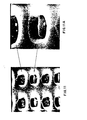
- An exposure of a via 12A corresponding to the E-beam spot is shown in Fig. 3A.
- the exposure can be effected in one pass at an energy of from about 20KV to 30KV at exposure times (e.g. 220 nanoseconds) to provide dosage levels of from about 5 to 20 coulomb/cm 2 , as for example 10 coul/cm normally at a beam current of 3 microamps.
- With lower energy levels the exposure can be effected with a plurality of passes at the via site 12A.
- a plurality of overlapping via targets can be employed, as for example the four exposed via sites 12B, 12C, 12D and 12E as shown in Fig. 3B.
- the image resist layer 11 is developed in an alkaline medium, such as 1:3 mix of the Shipley AZ 2401 with D.I. water, at a low temperatures of 14.5+0.1°C, followed by a DI H 2 0 rinse and a blow dry.
- This operation removes the latent image portions 12 of the image resist layer 11, which were exposed by the E-beam to form the access windows 13 to expose the underlying layer 10 as shown in Fig. 4.
- Generally 5000 x 5000nm latent images require from about 8 to about 10 minutes development time.
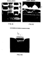
- the rectangular configurations of the vias in a test site is shown in Fig. 9.
- the units are then subjected to a controlled post-bake, which can be effected at l25°C+3° for about 40 minutes in a suitable oven suitably heated to temperature at a thermal rise time of about 2 to about 10°C per minute.
- the units can be post-baked in three steps: for 20 minutes at 85+5°C (hot plate); for 20 minutes at 115+5°C (oven/air ambient); and for 20 minutes at 145+5°C (oven/air).
- This post baking enables controlled flow of the image resist to transform the rectangular image via openings (Fig. 9) to properly tapered and rounded configurations as shown in Fig. 10.
- the portion of the resist underlayer 10 are then RIE etched in a suitable ambient e.g. CF 4 +0 2 forming a via opening 14 (Fig. 5) to expose corresponding portions of the quartz layer 4, which is also RIE etched in a suitable ambient, e.g. CF 4 +0 2 to open the via hole 15 over the conductor stripe 7 as shown in Figs. 6 and 11 to 11B.
- a suitable ambient e.g. CF 4 +0 2
- the remaining portions of the image resist layer 11 and the underlayer 10 are then stripped in any suitable manner, as by RF ashing in 1.333 mbar 5 ccm 0 2/ min flow at 250 watts for 35 minutes.
- the stripped unit is then cleaned in chromic/nitric acid solution for 5 minutes at room temperature, DI-H 2 0 rinsed and N 2 blown dry to provide the structure of Fig. 7.
- a second level of metallization 16 is then deposited with a via connection 17, in the via hole 15, to interconnect with the first level of metallization as presented by the conductor stripe 7.
- the deposition of the second level metallization 16/17 can be accomplished either by lift-off processes or by blanket coating followed by substractive etching.
Abstract
Description
- This invention relates to the formation of a pattern of openings in a layer of a positive resist system on semiconductor devices using high energy electron beam radiation, and more particularly to the development of said exposed resist layer with horizontal and vertical control of the hole dimensions. Furthermore, the invention relates to a method of forming via holes.
- Advances in modern semiconductor device technology have allowed increasing numbers of devices and circuits to be fabricated within a single semiconductor chip. This has required increasing microminiaturization of both the semiconductor elements as well as the interconnection metallurgy which connect the elements within the chip into circuits. Such miniaturization results in decreased costs and improved performance in integrated circuits; but it is constantly crowding the fabrication technology, particularly the photolithographic and etching techniques of the interconnection metallurgy.
- In integrated circuit logic and memory design, for example many thousands of impurity regions are conventionally fabricated in a silicon chip approximately 3 to 5 mm square. Such regions form transistors, diodes, resistors and the like which are then connected together by the metallurgical patterns atop the chip to form various circuits and for connection to input-output terminals.
- This interconnection metallurgy system atop the chip is extremely complex and usually employs two or three separate levels of complex thin film conductor patterns, each separated by one or more layers of dielectric, material. Ordinarily, the first level conductive patterns on the chip surface interconnects the transistors, resistors, diodes, etc. into circuits and also provides for circuit-to-circuit connections. The latter function is usually provided by parallel conductive lines connected to the individual circuits. The second level conductive pattern conventionally completes the circuit-to-circuit connection and makes contact to I/O terminals which are connectable to a support such as a module, substrate or card. The second level usually consists of parallel lines that are transverse to the aforementioned parallel lines of the underlying first level conductive pattern. In advanced designs third, and even fourth, levels may be required for power and I/O connections.
- At present it is necessary to etch the dielectric layers to form feedthrough patterns from one level to another. The standard process of interconnecting one level of metallurgy to another involves depositing an insulator such as Si02 atop a first level metallurgical pattern disposed on a substrate. The glass is typically deposited pyroly- tically, although the sputtered glass position process described in US Patent No. 3,983,022.
- A photoresist layer is then deposited, exposed and developed so that the via hole pattern is formed in the photoresist over the glass. The exposed glass portions are then etched to form the via holes down to the first level metallurgy. A second level metallurgical pattern is then deposited atop the remaining glass layer and into the via holes for connection to the first level pattern. The formation of positive resist masks from layers of ra- diat..on degradable polymers is described, for example, by Haller and Hatzakis in US Patent No. 3,535,137. A radiation degradable polymer layer is coated on a substrate and is subjected to patternwise exposure by high energy radiation such as, for example, x-rays, nuclear radiation, and electrons. The irradiated regions of the polymer suffer a decrease in molecular weight and therefore become more rapidly soluble. A developer is then used to preferentially remove the irradiated portions of the layer. The substrate is then subjected to an additive or substractive process such as metallization of etching of said substrate with the remaining portions of the resist layer acting to protect the substrate.
- Techniques have also been described by others for forming via holes for interconnection of several metal layers using reactive ion etching (RIE) of quartz insulator layers accompanied by suitable photolithographic processing, as described by J.A. Bondur et al in their "Step Coverage Process with Projection Printing and Reactive Ion Etching" and "Step Coverage Process with Reactive Ion Etching Using Thermal Resist Effects", respectively, pages 3415-16 and 3413-14 of the February 1977 IBM-Technical Disclosure Bulletin, Volume 19, No.9. As brought out therein, for reliable step coverage of a metal interconnection layer, etched insulator (oxide, quartz, etc.) slope angles of 50° to 60° are desirable in the via holes.
- When using electron beam (E-beam) lithography in conjunction with reactive ion etching (RIE), one cannot utilize the same resist process as for optical (e.g. UV) exposure.
- There are many complications which arise when E-beam lithography is used with RIE to form properly imaged and tapered via holes in insulator layers, such as Si02, quartz, polyimides and the like. For example, acrylic resists have RIE rates which are too high to make them effective masks in etching thick quartz layers for forming via-holes, whereas resists which serve as good RIE masks come from the novolak family such as Shipley's AZ 1350J, AZ 111, and the like, including a preferred resist system (hereinafter referred to as "HC") comprised of a cresol/ formaldehyde and a diazo-benzophenone sensitizer, specifically 2,4-bis-(6-diazo-5,6-dihydro-5-oxo-l-naphthalenesulfonyl)-benzophenone sensitizer.
- Processing E-beam exposed novolak resist, as for example the HC resist, is more complicated and demanding than processing the optically exposed forms. While development times for optical exposure are in the range of 0.5 to 2.0 minutes, E-beam exposure necessitates development times in the neighborhood of 8 to 10 minutes. These longer development times require an extremely good bond between the resist and substrate to avoid adhesion loss in the developer. Even the polysulfone adhesion layer used for optical lithographic processes becomes inadequate at the longer development times. Also, due to long development times the novolak (e.g. HC) resists have a tendency to de-adhere from some substrates, (e.g. quartz and oxide layers) during development.
- The invention as claimed is intended to remedy these drawbacks.
- Object of the invention is an improved method of forming a pattern of openings in a layer of a positive resist system and a method of forming via holes.
- The objects of the invention are achieved by methods according to claims 1 and 8.
- The advantages offered by the invention are improved control of hole formation in the resist layer and improved control of the horizontal and vertical dimensions of via hole formation in insulating layers, and particularly the formation of via-holes with improved sidewall taper, especially for small via hole geometrics.
- In the accompanying drawings forming a material part of this disclosure:
- Figs. 1 to 8 are diagrammatic cross-sectional views illustrating various stages of the masking technique of this invention, with
- Figs. 3A to 3C are explanatory views of Fig.3.
- Figs. 9 to 11B are photographic enlargements of test devices processed in accordance with this invention.
- For further comprehension of the invention, and of the objects and advantages thereof, reference will be made to the following description and accompanying drawings and the appended claims in which the novel features of the invention are more particularly set forth.
- In accordance with the invention, there is provided a novel process or method for the specific purpose of reactive ion etching vias in insulating layers using E-beam lithography which substantially eliminates the disadvantages of the prior art, with specific application for reactive ion etching first level via-holes for interconnecting multilevel metallurgical patterns of integrated circuit substrates.
- The invention comprises several critical processing steps, which taken as a whole, constitute the E-beam first via RIE process of this invention. The significant value of this invention is that as a whole, it meets its objectives only through the intricate interrelationship between the individual steps. The process is complex and each processing step has an effect on the others since the optimization of the process is achieved by designing each step to complement the others, which reproducibly forms vias whose horizontal dimensions are accurately controlled with vias having the proper vertical taper to insure second metal coverage and in turn, adequate reliability.
- Although not required for polyimide insulating layers, with the use of insulating layers such as quartz and Si02, the invention initially requires the application of an adhesion promoter prior to the application of the imaging resist proper. A particularly effective adhesion promoter, for purposes of this invention is an underlay of about 100 to about 200nm, typically of about 140nm, of Eastman Kodak's KMR resist which is a sensitized partially cyclized poly-cis-isoprene. This KMR resist underlay or layer is baked, e.g. about 160°C, to desensitize it during the bake cycle. The purpose of the underlay is to increase adhesion of the imaging resists, to quartz and Si02, during the development cycle. This KMR layer remains intact during resist development cycle, but is removed in the vias during the initial stages of the RIE operation.
- The KMR resist is overcoated with a layer of a novolak imaging resist system (e.g. HC resist) which is sufficiently sensitive to an E-beam exposure density of about 5 to about 20 (e.g. 10) u coulomb/cm2, and which is not severely degraded during the RIE operation. The imaging resist can be applied in thicknesses of about 2000 to about 3000nm, which illustratively for the HC resist would be about 2500nm. The imaging resist should also have a high ratio of development rate of exposed resist to the development rate of unexposed resist (R/Ro).
- The imaging resist is then controllably E-beam exposed in accordance with the required via pattern. Occasionally images are exposed which are not integral multiples of the E-beam spot size. In such case, proper image size and sidewall taper can be achieved by suitable "graying" of the E-beam exposure. As used herein "graying" is reducing or increasing E-beam exposure times for each nominal via size, depending upon the desired size of that particular via.
- Graying also enables vias with multiple spot overlap to be developed and baked at the same conditions as the non-overlapped vias.
- This invention also comprehends special resist developing parameters, which minimize imaging resist loss in the unexposed regions, and more importantly, to enable proper control of the developed image, both in the horizontal dimensions and sidewall taper. The developing is accomplished by utilizing a suitable developer, such as Shipley's commercially available KOH based AZ-1301 diluted with water in a 1:3 proportion, and developing at low temperatures in the range of about 13 to about 15°C, and illustratively of about 14°C.
- Also contemplated is the use of develop end point detection (DEPD) techniques such as described by H.A. Khoury et al in "Front Wafer Registration Device for Batch Process Etch End-Point Detection System" pp.1756-59 of the October 1977 IBM-TDB, Vol. 20, No.5, and by D.H. Jurczyk et al in "Process Detection System" pp.1867-70 of the November 1975 IBM-TDB, Vol. 18, No. 6.
- The use of the DEPD enables reproducible image size control despite variations in pre-bake temperatures, resist development rates, E-beam exposure density, ambient light conditions, strength of developer and resist thickness. Developing times will vary based on the parameters noted above, and developing for fixed times will result in loss of image size integrity. The DEPD technique utilized in this process comprises the use of a suitably designed or dedicated test site with metal line widths and spaces characteristic of the product dimensions. More importantly, the technique utilizes the concept of DEPD "over-develop" which is in actuality a relationship between the time to develop in the test site vs. the time to properly open a via. Thus, the substrates or wafers are developed for a given time past full development of the resist in the test site. This additional time is referred to as At and is a certain percentage of the time to reach end-point in the test site. The determination of the value of At depends on several parameters, namely material properties and tool characteristics.
- More importantly, it depends on the via image size, which are exposed, and the exposure gray levels. By proper combination of gray level and Δt, all images on the wafer can be developed to specification. Typically, the overde- velop time, Δt, can be from about 10 to about 100%, and preferably from about 20 to about 40% of the time to reach end-point in the test site.
- An additional important stage of this invention is controlled resist baking after development to properly cure and form the resist image. The baking cycle must be of such a nature as to controllably flow the resist to achieve a suitable sidewall taper, which will be reproduced in the insulator (e.g. quartz) layer during RIE. The baking cycle must also be of such a nature as to maintain proper horizontal dimensional control. Such a bake cycle can be achieved by a gradual heating over a time in the range of about 20 to about 60 minutes at a temperature of about 120 to about 160°C. One way of arriving at the bake temperature is by use of an oven set at a temperature of about 120 to about 140°C with a thermal rise time of about 2 to about 10°C per minute. The same baking effect can also be achieved by a three step bake at temperatures of about 80 to about 90°C, as for example, about 85°C, (e.g. hot plate) for about 10 to about 20 minutes, at about 100 to about 120°C, as for an example, 115°C (e.g. in an oven) for about 10 to about 20 minutes followed by a final bake at about 130 to about 160°C, as example of about 150°C (e.g. in an oven) for about 10 to about 20 minutes.
- After development, the wafer or substrate is reactive ion etched to transfer the via of the resist through the desensitized resist underlayer to the insulating layer, e.g. quartz, in a diode or other suitably configured system in a CF4 +02 gas ambient.
- The process of this invention, if used correctly, has the ability to transform an E-beam exposed "square" via into a properly tapered "round" via hole, Fig. 3C. This process also enables tight control of horizontal dimensions of all different and varied via sizes exposed and etched on a wafer or substrate. Use of this process has produced dimensional control resulting in a 500 nm tolerance on etched vias.
- In addition, the process disclosed and described herein either solves or eliminates the following problem:
- Steep vertical profiles of etched vias result in reduced and unacceptable second level metal electromigration lifetimes. In contrast, this process produces properly tapered round vias from initially exposed square images. Proper shape and taper of the vias is produced by a low temperature develop stage and by a controlled image resist baking procedure;
- A minimum thickness of the image resist layer to mask the RIE operation is needed. To achieve this, one can increase the initial thickness of the resist, which is impractical since it interferes with E-beam registration and also results in excessively long developing times. One can also use the technique of interrupted developing, whereby the Ro is artificially decreased by developing the wafer or substrate in steps. This is impractical since it does not lend itself to commercial manufacturing operations, and because the material characteristics (e.g. resist and developer) are not consistent enough to accurately specify the correct cycle times. The solution of this invention which is most practical and works best is a low temperature develop, which provides a suitable R/Ro, which leaves adequate resist after development and baking to mask the RIE operation;
- The ability to achieve reproducible and controlled image sizes, especially for small via geometries (approximately 5 m), is one of the prime driving forces to use RIE. It is also one of the most difficult to achieve. The process of this invention produces a well controlled and very reproducible vias by the combination of "grayed" E-beam exposure, proper DEPD technique, low temperature develop, and controlled resist bake after development.
- With reference to the drawings, Fig. 1 shows a cross-section of thin
metallic films 6 and 7 of approximately 1 um in thickness disposed on top of aninsulative coating 2 of a substrate 1 and covered by a dielectric layer 4 (e.g. quartz) having a suitable thickness, as for example 2 to 2.5 um.Films 6 and 7 comprise a portion of a first level conductive pattern which is generally interconnected through theinsulator coating 2 to doped impurity regions within a semiconductor substrate 1 (not shown).Films 6 and 7 are also normally interconnected to other such films in said pattern on the same level to form device-to-device and circuit-to-circuit interconnections, as is well known in the art. One method of forming such films, 6 and 7 is by a lift-off method as described in US patent 4,004,044. -
Films 6 and 7 typically comprise aluminum, aluminum-copper alloys, alluminum-copper-silicon alloys as illustrative of other conductive films which can also be used. -
Dielectric layer 4, as indicated can be a polyimide, Si02, glass or quartz or other suitable insulating composition employed in the art. Quartz is selected for purposes of this description, and which can be formed by conventional R.F. or D.C. sputtering techniques to cover the thin film pattern atop the substrate. If required, the quartz coating can be planarized by the technique described in US Patent No. 3,983,022. As will be understood, the substrate indicated in the drawings is a portion of an integrated circuit chip which is replicated in large number in a mother sheet or wafer. - In preparation for via hole formation the substrate/wafer, after inspection of the
insulator coating 4, is cleaned in a chromic/nitric acid solution for sufficient time, e.g. about 5 minutes at room temperature followed by a D.I.H20 and blown dry, with a subsequent bake in an N2 ambient oven for 30 minutes at about 160°C+5°. - For surface preparation, the dried wafer was then static flooded with trifluoro-amino-silane followed by spinning at 5500 RPM for 30 seconds. This is followed by the application of the Kodak KMR resist from 1:4 solution in xylene with spinning for 60 seconds at 4000 RPM which results in a coating of about 150 to 180 nm + l5nm, which after baking on a hotplate at 160°C+5° for 30 minutes becomes desensitized to form the
adhesion promoting underlayer 10. - At this point, the "HC" image resist
layer 11 is applied from a solution of diglyme with spinning at 2200 RPM for 60 seconds to form a coating thickness of 2650+75nm, with a nominal target of 2 to 3 microns. The resist is then prebaked suitably, as on a hot plate at 85+3°C for 30 minutes. - The exposure of the image resist
layer 11 is accomplished by a 2500nm square E-beam in the desired pattern ofopenings 12 at appropriate voltage and dosage levels. An exposure of a via 12A corresponding to the E-beam spot is shown in Fig. 3A. The exposure can be effected in one pass at an energy of from about 20KV to 30KV at exposure times (e.g. 220 nanoseconds) to provide dosage levels of from about 5 to 20 coulomb/cm2, as for example 10 coul/cm normally at a beam current of 3 microamps. With lower energy levels the exposure can be effected with a plurality of passes at the via site 12A. For larger vias with larger dimensions a plurality of overlapping via targets can be employed, as for example the four exposed viasites - After exposure, the image resist
layer 11 is developed in an alkaline medium, such as 1:3 mix of the Shipley AZ 2401 with D.I. water, at a low temperatures of 14.5+0.1°C, followed by a DI H20 rinse and a blow dry. This operation removes thelatent image portions 12 of the image resistlayer 11, which were exposed by the E-beam to form theaccess windows 13 to expose theunderlying layer 10 as shown in Fig. 4. Generally 5000 x 5000nm latent images require from about 8 to about 10 minutes development time. The rectangular configurations of the vias in a test site is shown in Fig. 9. - In accordance with the invention, the units are then subjected to a controlled post-bake, which can be effected at l25°C+3° for about 40 minutes in a suitable oven suitably heated to temperature at a thermal rise time of about 2 to about 10°C per minute. Alternatively, the units can be post-baked in three steps: for 20 minutes at 85+5°C (hot plate); for 20 minutes at 115+5°C (oven/air ambient); and for 20 minutes at 145+5°C (oven/air). This post baking enables controlled flow of the image resist to transform the rectangular image via openings (Fig. 9) to properly tapered and rounded configurations as shown in Fig. 10.
- The portion of the resist
underlayer 10 are then RIE etched in a suitable ambient e.g. CF4+02 forming a via opening 14 (Fig. 5) to expose corresponding portions of thequartz layer 4, which is also RIE etched in a suitable ambient, e.g. CF4+02 to open the viahole 15 over the conductor stripe 7 as shown in Figs. 6 and 11 to 11B. During the RIE operation, the taper of the rounded viaopenings 13A in the image resistlayer 11 is transferred to the viahole 15 in thequartz layer 4. - The remaining portions of the image resist
layer 11 and theunderlayer 10 are then stripped in any suitable manner, as by RF ashing in 1.333 mbar 5 ccm 02/min flow at 250 watts for 35 minutes. The stripped unit is then cleaned in chromic/nitric acid solution for 5 minutes at room temperature, DI-H20 rinsed and N2 blown dry to provide the structure of Fig. 7. - After inspection of the wafers, a second level of
metallization 16 is then deposited with a viaconnection 17, in the viahole 15, to interconnect with the first level of metallization as presented by the conductor stripe 7. The deposition of thesecond level metallization 16/17 can be accomplished either by lift-off processes or by blanket coating followed by substractive etching. - While the invention has been illustrated and described with preferred embodiments of this invention, it is to be understood that the invention is not to be limited to the precise construction herein disclosed and the right is reserved to all changes and modifications coming within the scope of the invention as defined in the appended claims.
Claims (10)
characterized in that
characterized in that
the heating of the developed resist is performed in a step-wise manner, with a first bake at a temperature of about 80 to 90 + 5°C for about 10 to 20 minutes, a second bake at a temperature of about 100 to 120 + 5°C for about 10 to 20 minutes, and a bake at said final temperature for about 10 to 20 minutes.
characterized in that
said heating is raised to said final temperature at
a thermal rise time of about 2 to 10°C per minute, with a bake at said final temperature for about 20 to 60 minutes.
characterized in that
the positive resist system (11) is applied to polyimide dielectric layer (4) disposed on substrate (2).
characterized in that
when a quartz or silicon dioxide dielectric layer (4) is disposed on substrate (2) an intervening adhesion layer (10) is formed on said quartz layer prior to formation of resist layer (11).
characterized in that
adhesion layer (10) comprises a partially cyclized polycis-isoprene photoresist desensitized by heating prior to the forming of positive resist layer (11).
characterized in that
the positive resist system is a cresol/formaldehyde novolak containing a 2,4-bis-(6-diazo-5,6-dihydro-5-oxo-l-naphtalene-sulfonoxy)-benzophenone-sensitizer.
characterized in that
the dielectric insulating coating (4) is a polyimide coating.
characterized in that
the dielectric insulating coating (4) is a quartz or silicon dioxide coating to which, prior to forming resist layer (11), an intervening layer (10) of an adhesion promoter is applied, said intervening layer (10), prior to etching of coating (4), being reactive ion etched through openings (13).
Applications Claiming Priority (2)
| Application Number | Priority Date | Filing Date | Title |
|---|---|---|---|
| US283695 | 1981-07-15 | ||
| US06/283,695 US4409319A (en) | 1981-07-15 | 1981-07-15 | Electron beam exposed positive resist mask process |
Publications (3)
| Publication Number | Publication Date |
|---|---|
| EP0069854A2 true EP0069854A2 (en) | 1983-01-19 |
| EP0069854A3 EP0069854A3 (en) | 1983-06-22 |
| EP0069854B1 EP0069854B1 (en) | 1985-10-23 |
Family
ID=23087160
Family Applications (1)
| Application Number | Title | Priority Date | Filing Date |
|---|---|---|---|
| EP82104711A Expired EP0069854B1 (en) | 1981-07-15 | 1982-05-28 | Method of forming via holes in insulating layers |
Country Status (6)
| Country | Link |
|---|---|
| US (1) | US4409319A (en) |
| EP (1) | EP0069854B1 (en) |
| JP (1) | JPS5844720A (en) |
| CA (1) | CA1173689A (en) |
| DE (1) | DE3267000D1 (en) |
| ES (1) | ES513051A0 (en) |
Cited By (2)
| Publication number | Priority date | Publication date | Assignee | Title |
|---|---|---|---|---|
| EP0134453A2 (en) * | 1983-07-08 | 1985-03-20 | International Business Machines Corporation | Method for exposure dose calculation of photolithography projection printers |
| GB2228582A (en) * | 1989-02-23 | 1990-08-29 | Mitsubishi Electric Corp | Method for producing patterns in silicone ladder type resin |
Families Citing this family (31)
| Publication number | Priority date | Publication date | Assignee | Title |
|---|---|---|---|---|
| GB2137808A (en) * | 1983-04-06 | 1984-10-10 | Plessey Co Plc | Integrated circuit processing method |
| JPS60114575A (en) * | 1983-11-28 | 1985-06-21 | Tokyo Ohka Kogyo Co Ltd | Formation of dry pattern |
| US4560436A (en) * | 1984-07-02 | 1985-12-24 | Motorola, Inc. | Process for etching tapered polyimide vias |
| JPS6148883A (en) * | 1984-08-16 | 1986-03-10 | Toppan Printing Co Ltd | Manufacture of rainbow hologram using photoresist |
| US4592132A (en) * | 1984-12-07 | 1986-06-03 | Hughes Aircraft Company | Process for fabricating multi-level-metal integrated circuits at high yields |
| JP2517707B2 (en) * | 1985-03-04 | 1996-07-24 | ソニー株式会社 | Method of forming photoresist pattern |
| US4671849A (en) * | 1985-05-06 | 1987-06-09 | International Business Machines Corporation | Method for control of etch profile |
| US4827867A (en) * | 1985-11-28 | 1989-05-09 | Daikin Industries, Ltd. | Resist developing apparatus |
| US4762805A (en) * | 1985-12-17 | 1988-08-09 | Advanced Micro Devices, Inc. | Nitride-less process for VLSI circuit device isolation |
| US4863827A (en) * | 1986-10-20 | 1989-09-05 | American Hoechst Corporation | Postive working multi-level photoresist |
| US4822755A (en) * | 1988-04-25 | 1989-04-18 | Xerox Corporation | Method of fabricating large area semiconductor arrays |
| US6288561B1 (en) * | 1988-05-16 | 2001-09-11 | Elm Technology Corporation | Method and apparatus for probing, testing, burn-in, repairing and programming of integrated circuits in a closed environment using a single apparatus |
| US5103557A (en) * | 1988-05-16 | 1992-04-14 | Leedy Glenn J | Making and testing an integrated circuit using high density probe points |
| US5225771A (en) * | 1988-05-16 | 1993-07-06 | Dri Technology Corp. | Making and testing an integrated circuit using high density probe points |
| US5068959A (en) * | 1988-07-11 | 1991-12-03 | Digital Equipment Corporation | Method of manufacturing a thin film head |
| US5166771A (en) * | 1990-01-12 | 1992-11-24 | Paradigm Technology, Inc. | Self-aligning contact and interconnect structure |
| US5483104A (en) * | 1990-01-12 | 1996-01-09 | Paradigm Technology, Inc. | Self-aligning contact and interconnect structure |
| US5174857A (en) * | 1990-10-29 | 1992-12-29 | Gold Star Co., Ltd. | Slope etching process |
| US5296333A (en) * | 1990-11-16 | 1994-03-22 | Raytheon Company | Photoresist adhesion promoter |
| US5935734A (en) * | 1997-03-03 | 1999-08-10 | Micron Technology, Inc. | Method for fabrication of and apparatus for use as a semiconductor photomask |
| JPH11289103A (en) * | 1998-02-05 | 1999-10-19 | Canon Inc | Semiconductor device and solar cell module and their overhauling methods |
| US6606533B1 (en) | 2000-10-12 | 2003-08-12 | International Business Machines Corporation | Method and arrangement for controlling image size of integrated circuits on wafers through post-exposure bake hotplate-specific dose feedback |
| AUPR451601A0 (en) * | 2001-04-20 | 2001-05-24 | Fawcett, Alan John | Method and apparatus for the hardening of photopolymer plates |
| JP2002353195A (en) * | 2001-05-23 | 2002-12-06 | Sony Corp | Method of manufacturing semiconductor device |
| EP1273973A1 (en) * | 2001-07-03 | 2003-01-08 | Infineon Technologies SC300 GmbH & Co. KG | Method for adjusting a temperature in a resist process |
| JP4876341B2 (en) * | 2001-07-13 | 2012-02-15 | 日本電気株式会社 | Active matrix substrate and manufacturing method thereof |
| GB2387026A (en) * | 2002-03-28 | 2003-10-01 | Zarlink Semiconductor Ltd | Method of coating contact holes in MEMS and micro-machining applications |
| JP2005196130A (en) * | 2003-12-12 | 2005-07-21 | Hitachi Cable Ltd | Photosensitive polyimide resin composition, insulating film using the same, process for producing insulating film, and electronic component using the insulating film |
| CN100370580C (en) * | 2004-03-29 | 2008-02-20 | 雅马哈株式会社 | Semiconductor wafer and its producing method |
| DE102004052611A1 (en) * | 2004-10-29 | 2006-05-04 | Infineon Technologies Ag | Method for producing an opening at least partially filled with a filling material, method for producing a memory cell and memory cell |
| US7973413B2 (en) * | 2007-08-24 | 2011-07-05 | Taiwan Semiconductor Manufacturing Company, Ltd. | Through-substrate via for semiconductor device |
Family Cites Families (11)
| Publication number | Priority date | Publication date | Assignee | Title |
|---|---|---|---|---|
| US3549368A (en) * | 1968-07-02 | 1970-12-22 | Ibm | Process for improving photoresist adhesion |
| US3751248A (en) * | 1971-12-27 | 1973-08-07 | Bell Telephone Labor Inc | Method of selective multilayered etching |
| US3852771A (en) * | 1973-02-12 | 1974-12-03 | Rca Corp | Electron beam recording process |
| JPS49116976A (en) * | 1973-03-09 | 1974-11-08 | ||
| US3961101A (en) * | 1974-09-16 | 1976-06-01 | Rca Corporation | Process for improved development of electron-beam-sensitive resist films |
| DE2447225C2 (en) * | 1974-10-03 | 1983-12-22 | Ibm Deutschland Gmbh, 7000 Stuttgart | Process for peeling off positive photoresist |
| JPS5261482A (en) * | 1975-11-17 | 1977-05-20 | Mitsubishi Electric Corp | Photo etching |
| JPS6026294B2 (en) * | 1977-09-26 | 1985-06-22 | 株式会社日立製作所 | Photo etching method |
| US4212935A (en) * | 1978-02-24 | 1980-07-15 | International Business Machines Corporation | Method of modifying the development profile of photoresists |
| US4184909A (en) * | 1978-08-21 | 1980-01-22 | International Business Machines Corporation | Method of forming thin film interconnection systems |
| JPS5626434A (en) * | 1979-08-10 | 1981-03-14 | Oki Electric Ind Co Ltd | Forming method for pattern of semiconductor substrate |
-
1981
- 1981-07-15 US US06/283,695 patent/US4409319A/en not_active Expired - Lifetime
-
1982
- 1982-05-28 DE DE8282104711T patent/DE3267000D1/en not_active Expired
- 1982-05-28 EP EP82104711A patent/EP0069854B1/en not_active Expired
- 1982-05-28 CA CA000404032A patent/CA1173689A/en not_active Expired
- 1982-06-14 ES ES513051A patent/ES513051A0/en active Granted
- 1982-06-18 JP JP57104025A patent/JPS5844720A/en active Granted
Non-Patent Citations (6)
| Title |
|---|
| IBM JOUNRAL OF RESEARCH AND DEVELOPMENT, vol. 21, no. 3, May 1977, pages 210-218, New York (USA); F.H. DILL et al. "Thermal effects on the photoresist AZ135OJ" * |
| IBM JOURNAL OF RESEARCH AND DEVELOPMENT, vol. 21, no. 3, May 1977, pages 210-218, New York (USA); F.H. DILL et al.: "Thermal effects on the photoresist AZ1350J" * |
| IBM TECHNICAL DISCLOSURE BULLETIN, vol. 16, no. 1, June 1973, page 47, New York (USA); H. G. BICKFORD et al. "Blocking process for photoresist" * |
| IBM TECHNICAL DISCLOSURE BULLETIN, vol. 23, no. 7A, December 1980, page 2767, New York (USA); W.T. BABIE et al. "End-point detection of resist development fiducial dosage adjustment" * |
| J. ELECTROCHEM. SOC.: SOLID-STATE SCIENCE AND TECHNOLOGY, vol. 126, no. 11, November 1979, pages 2026-2031, Princeton N.Y. (USA); J.M. SHAW et al. "Developer temperature effects on E-beam and optically exposed positive photoresist" * |
| PHOTOGRAPHIC SCIENCE AND ENGINEERING, vol. 21, no. 5, September-October 1977, pages 290-292, Washington D.C. (USA); K. JINNO et al. "Baking characteristics of positive photoresist" * |
Cited By (5)
| Publication number | Priority date | Publication date | Assignee | Title |
|---|---|---|---|---|
| EP0134453A2 (en) * | 1983-07-08 | 1985-03-20 | International Business Machines Corporation | Method for exposure dose calculation of photolithography projection printers |
| EP0134453A3 (en) * | 1983-07-08 | 1985-07-24 | International Business Machines Corporation | Method for exposure dose calculation of photolithography projection printers |
| GB2228582A (en) * | 1989-02-23 | 1990-08-29 | Mitsubishi Electric Corp | Method for producing patterns in silicone ladder type resin |
| US5087553A (en) * | 1989-02-23 | 1992-02-11 | Mitsubishi Denki Kabushiki Kaisha | Method for transferring patterns on silicone ladder type resin and etching solution used in such method |
| GB2228582B (en) * | 1989-02-23 | 1993-06-16 | Mitsubishi Electric Corp | Methods of producing patterns in silicone ladder resins |
Also Published As
| Publication number | Publication date |
|---|---|
| JPS5844720A (en) | 1983-03-15 |
| US4409319A (en) | 1983-10-11 |
| JPS6357941B2 (en) | 1988-11-14 |
| ES8308155A1 (en) | 1983-08-01 |
| CA1173689A (en) | 1984-09-04 |
| EP0069854B1 (en) | 1985-10-23 |
| EP0069854A3 (en) | 1983-06-22 |
| DE3267000D1 (en) | 1985-11-28 |
| ES513051A0 (en) | 1983-08-01 |
Similar Documents
| Publication | Publication Date | Title |
|---|---|---|
| EP0069854B1 (en) | Method of forming via holes in insulating layers | |
| US5240878A (en) | Method for forming patterned films on a substrate | |
| US6372412B1 (en) | Method of producing an integrated circuit chip using frequency doubling hybrid photoresist and apparatus formed thereby | |
| US5250375A (en) | Photostructuring process | |
| Lin et al. | Practicing the Novolac deep‐UV portable conformable masking technique | |
| US5334487A (en) | Method for forming a patterned layer on a substrate | |
| EP0370935A2 (en) | Method of forming conductive lines and studs | |
| JPH06326222A (en) | Method for forming via and groove with high aspect ratio in optical image forming material or photoresist material | |
| EP0142639A2 (en) | Method for forming narrow images on semiconductor substrates | |
| US5127989A (en) | Method of forming a thin film pattern with a trapezoidal cross section | |
| EP0072933B1 (en) | Method for photolithographic pattern generation in a photoresist layer | |
| US6340635B1 (en) | Resist pattern, process for the formation of the same, and process for the formation of wiring pattern | |
| EP0021719B1 (en) | Method for producing negative resist images, and resist images | |
| US5326670A (en) | Process for forming resist pattern | |
| EP0349411A2 (en) | Photoresists resistant to oxygen plasmas | |
| EP0199303B1 (en) | Method of forming a photoresist pattern | |
| US5114827A (en) | Photoresists resistant to oxygen plasmas | |
| US6866988B2 (en) | Methods for measuring photoresist dimensions | |
| JPH0795509B2 (en) | Method of forming resist pattern | |
| JPH06110214A (en) | Formation of resist pattern | |
| US3669669A (en) | Cyclic polyisoprene photoresist compositions | |
| JPH02156244A (en) | Pattern forming method | |
| Pavelchek et al. | Processing techniques for improving performance of positive-tone silylation | |
| JPH042183B2 (en) | ||
| Neisius et al. | Properties of a high resolution negative photoresist |
Legal Events
| Date | Code | Title | Description |
|---|---|---|---|
| PUAI | Public reference made under article 153(3) epc to a published international application that has entered the european phase |
Free format text: ORIGINAL CODE: 0009012 |
|
| AK | Designated contracting states |
Designated state(s): BE CH DE FR GB IT LI NL SE |
|
| PUAL | Search report despatched |
Free format text: ORIGINAL CODE: 0009013 |
|
| AK | Designated contracting states |
Designated state(s): BE CH DE FR GB IT LI NL SE |
|
| 17P | Request for examination filed |
Effective date: 19830519 |
|
| GRAA | (expected) grant |
Free format text: ORIGINAL CODE: 0009210 |
|
| AK | Designated contracting states |
Designated state(s): BE CH DE FR GB IT LI NL SE |
|
| PG25 | Lapsed in a contracting state [announced via postgrant information from national office to epo] |
Ref country code: NL Effective date: 19851023 Ref country code: BE Effective date: 19851023 |
|
| PG25 | Lapsed in a contracting state [announced via postgrant information from national office to epo] |
Ref country code: SE Effective date: 19851030 |
|
| REF | Corresponds to: |
Ref document number: 3267000 Country of ref document: DE Date of ref document: 19851128 |
|
| ITF | It: translation for a ep patent filed |
Owner name: IBM - DR. ARRABITO MICHELANGELO |
|
| ET | Fr: translation filed | ||
| NLV1 | Nl: lapsed or annulled due to failure to fulfill the requirements of art. 29p and 29m of the patents act | ||
| PG25 | Lapsed in a contracting state [announced via postgrant information from national office to epo] |
Ref country code: LI Effective date: 19860531 Ref country code: CH Effective date: 19860531 |
|
| PLBE | No opposition filed within time limit |
Free format text: ORIGINAL CODE: 0009261 |
|
| STAA | Information on the status of an ep patent application or granted ep patent |
Free format text: STATUS: NO OPPOSITION FILED WITHIN TIME LIMIT |
|
| 26N | No opposition filed | ||
| REG | Reference to a national code |
Ref country code: CH Ref legal event code: PL |
|
| ITTA | It: last paid annual fee | ||
| PGFP | Annual fee paid to national office [announced via postgrant information from national office to epo] |
Ref country code: GB Payment date: 19920409 Year of fee payment: 11 |
|
| PGFP | Annual fee paid to national office [announced via postgrant information from national office to epo] |
Ref country code: FR Payment date: 19920427 Year of fee payment: 11 |
|
| PGFP | Annual fee paid to national office [announced via postgrant information from national office to epo] |
Ref country code: DE Payment date: 19920523 Year of fee payment: 11 |
|
| PG25 | Lapsed in a contracting state [announced via postgrant information from national office to epo] |
Ref country code: GB Effective date: 19930528 |
|
| GBPC | Gb: european patent ceased through non-payment of renewal fee |
Effective date: 19930528 |
|
| PG25 | Lapsed in a contracting state [announced via postgrant information from national office to epo] |
Ref country code: FR Effective date: 19940131 |
|
| PG25 | Lapsed in a contracting state [announced via postgrant information from national office to epo] |
Ref country code: DE Effective date: 19940201 |
|
| REG | Reference to a national code |
Ref country code: FR Ref legal event code: ST |