EP0102773B1 - Delay circuit arrangements - Google Patents
Delay circuit arrangements Download PDFInfo
- Publication number
- EP0102773B1 EP0102773B1 EP83304600A EP83304600A EP0102773B1 EP 0102773 B1 EP0102773 B1 EP 0102773B1 EP 83304600 A EP83304600 A EP 83304600A EP 83304600 A EP83304600 A EP 83304600A EP 0102773 B1 EP0102773 B1 EP 0102773B1
- Authority
- EP
- European Patent Office
- Prior art keywords
- signal
- delay
- output
- delayed
- demodulating
- Prior art date
- Legal status (The legal status is an assumption and is not a legal conclusion. Google has not performed a legal analysis and makes no representation as to the accuracy of the status listed.)
- Expired
Links
Images

Classifications
-
- H—ELECTRICITY
- H04—ELECTRIC COMMUNICATION TECHNIQUE
- H04N—PICTORIAL COMMUNICATION, e.g. TELEVISION
- H04N5/00—Details of television systems
- H04N5/14—Picture signal circuitry for video frequency region
- H04N5/20—Circuitry for controlling amplitude response
- H04N5/205—Circuitry for controlling amplitude response for correcting amplitude versus frequency characteristic
- H04N5/208—Circuitry for controlling amplitude response for correcting amplitude versus frequency characteristic for compensating for attenuation of high frequency components, e.g. crispening, aperture distortion correction
Definitions
- This invention relates to delay circuit arrangements suitable for contour compensation processing of video signals.
- the luminance signal contains a 3.58 MHz colour sub-carrier
- a 35.8 MHz beat brilliance variation results in the reproduced image.
- the video amplifier circuit in a colour television receiver has frequency characteristics such that the colour sub-carrier is attenuated by more than 15 to 16 dB.
- the high frequency components of the video signal are attenuated, resulting in reduction in the resolution of the reproduced image.
- the brilliance modulation efficiency tends to be reduced when the frequency exceeds 2 MHz. Such reduction of the brilliance modulation efficiency reduces the contrast, so reducing the resolution.
- a vertical contour compensation circuit 10 as shown in Figure 1 of the accopanying drawings has been used for improving the resolution of the image in the vertical direction thereof.
- an input luminance signal Y ln is supplied to a signal input terminal 1 to be fed to a delay line 2 and a first adder 3.
- the input luminance signal Y ln has a waveform as shown, for example, in Figure 2A of the accompanying drawings.
- the delay line 2 produces a first delayed luminance signal Y DL , having a waveform as shown in Figure 2B of the accompanying drawings, and which is delayed relative to the input luminance signal Y ln by one horizontal scanning period 1 H, and a second delayed luminance signal Y DL2 having a waveform as shown in Figure 2C of the accompanying drawings, which is delayed relative to the input luminance signal Y ln by 2 H.
- the first delayed luminanace signal Y DL1 obtained from the delay line 2 is fed to the subtracter 5 and a second adder 7.
- the second delayed luminance signal Y DL2 is fed to the first adder 3.
- the first adder 3 adds the input luminance signal Y ln and second delayed luminance signal Y DL2 , and feeds the resulting signal Y (having a waveform as shown in Figure 2D of the accompanying drawings) through an attenuator 4 to the subtracter 5.
- the subtracter 5 subtracts the signal Y A from the first delayed luminance signal Y DL1 to obtain a contour compensation sigal S AC having a waveform as shown in Figure 2E of the accompanying drawings.
- This contour compensation signal S AC is fed through a level controller 6 to the second adder 7.
- the second adder 7 superimposes the contour compensation signal S AC on the first delayed luminance signal Y DL1 and produces an output luminance signal Y out as shown in Figure 2F of the accompanying drawings.
- the signal Y out appears at an output terminal 8. It has a vertical contour compensated waveform with an overshoot and an undershoot resulting from the superimposition of the contour compensation signal S AC on the luminance change portions, that is, contour portions in the vertical direction of the image.
- the delay line 2 in the vertical contour compensation circuit 10 usually uses two 1 H delay lines 22 and 25 each providing a delay time equal to 1 H.
- the input luminance signal Y ln supplied to the input terminal 1 is fed to an amplitude modulator 21 in the delay line 2 for amplitude modulation.
- the output of the amplitude modulator 21 is fed to the first delay line 22.
- the delayed output signal from the first delay line 22 is fed through a first gain controlled amplifier 23 to a first demodulator 24.
- the first gain controlled amplifier 23 is gain controlled by the output of the first demodulator 24.
- the delayed output signal from the first delay line 22 is fed through the first gain controlled amplifier 23 to the second delay line 25.
- the delayed output signal from the second delay line 25 is fed through a second gain controlled amplifier 26 to a second demodulator 27.
- the first demodulator 24 demodulates the 1 H delayed luminance signal from the first delay line 22 and produces the first delayed luminance signal Y DL1 delayed by 1 H relative to the input luminance signal Y ln as shown in Figure 2B.
- the second demodulator 27 demodulates the luminance signal that has been delayed by 1 H in each of the first and second delay lines 22 and 25, and produces the second delayed luminance signal Y DL2 delayed by 2 H relative to the input luminance signal Y DL2 as shown in Figure 2C.
- the delay line 2 in the vertical contour compensation circuit 10 uses two 1 H delay lines 22 and 25 in order to obtain the first and second delayed luminance signals Y DL1 and Y DL2 delayed by 1 H and 2 H relative to the input luminance signal Y I" , respectively.
- delay lines are generally expensive, and the vertical contour compensation circuit 10, which used two high performance 1 H delay lines which are required to provide a comparatively long delay time and nevertheless have wide frequency band characteristics, is inevitably very expensive, the major part of the price being accounted for by the two delay lines.
- the signal level attenuation and temperature characteristics vary with invidual delay lines even of the same ratings and specifications. Therefore, where the two delay lines 22 and 25 are used as in the above case, the delayed output signals must be passed through the gain controlled amplifiers 23 and 26 for automatic level control.
- a delay circuit arrangement comprising:
- the illustrated vertical contour compensation circuit 100 incorporates a delay circuit 40, which employs a single 1 H delay line 43 which can provide first and second delayed luminance signals Y DL1 and Y DL2 respectively delayed 1 H and 2 H relative to an input luminance signal Y jn .
- a first adder 60 adds the input luminance signal Y in which is supplied to an input terminal 30 and the second delayed luminance signal Y DL2 .
- a subtracter 70 produces a contour compensation signal S AC from the first delayed luminance signal Y DL1 and the sum signal from the first adder 60.
- a second adder 80 superimposes the contour compensation signal S AC on the first delayed luminance signal Y DL1 to obtain a vertical contour compensated output luminance signal Y out .
- the delay circuit 40 also includes first and second amplitude modulators 41A and 41B for effecting so-called orthogonal modulation of a carrier from a carrier oscillator 50.
- the input luminance signal supplied to the input terminal 30 is fed to the first amplitude modulator 41A.
- the carrier output signal from the carrier oscillator 50 is supplied directly to the first amplitude modulator 41A, while it is supplied to the second amplitude modulator 41 B through a phase shifter 51 for shifting the phase by 90°.
- the orthogonal modulation is thus done with carriers 90° out of phase with each other to produce first and second amplitude modulated components S 1 and S 2 which are 90° out of phase with each other as shown in the vector diagram of Figure 4, these modulated components S 1 and S 2 being fed to an adder 42 to be added together.
- the resultant sum signal S A from the adder 42 is fed through the 1 H delay line 43 to a voltage controlled variable gain amplifier 44.
- the 1 H delay line 43 delays the sum signal S A by 1 H.
- the voltage controlled variable gain amplifier 44 effects insertion loss temperature compensation of the 1 H delay line, and it is gain controlled by the output of a reference signal detector 49 to be described later.
- the output of the voltage controlled variable gain amplifier 44 is fed to first and second demodulators 45A and 45B.
- the carrier output signal from the carrier oscillator 50 is suplied as a synchronizing signal through a voltage controlled variable phase shifter 52 to the first and second demodulators 45A and 45B for demodulating the sum signal output from the voltage controlled variable gain amplifier 44 by synchronous detection.
- a phase shifter 53 provides a phase difference of 90° between the synchronizing signals supplied to the demodulators 45A and 45B.
- the amount of phase shift by the voltage controlled variable phase shifter 52 is controlled by the output of a level comparator 55 to be described later.
- the first demodulator 45A demodulates only a component of the sum signal output of the voltage controlled variable gain amplifier 44 corresponding to the first amplitude modulation S 1 by synchronous detection of the sum signal output. It recovers the first delayed luminance signal YD11 delayed 1 H relative to the input luminance signal Y in , because the sum signal output fed to it from the variable gain amplifier 44 has been delayed 1 H through the 1 H delay line 43 and the first amplitude modulated component S 1 in the sum signal S A is the amplitude modulation of the input luminance signal Y ln on the carrier.
- the first delayed luminance signal Y DL1 from the first demodulator 45A is fed to the subtracter 70 and the second adder 80 as mentioned earlier. It is further fed through a clamp circuit 46 in the delay circuit 40 to a sample/hold circuit 54 and an adder 47.
- a reference signal S ⁇ coupled to a reference signal input terminal 48 is fed to the adder 47 to be superimposed on the first delayed luminance signal Y DL1 at a position corresponding to the blanking period as shown in Figure 5.
- the output of the adder 47 consisting of the reference signal S ⁇ and the first delayed luminance signal Y DLI superimposed on each other, is fed to the second amplitude modulator 41 B.
- the second demodulator 45B which corresponds to the second amplitude modulator 41 B, demodulates only a component of the sum signal output of the voltage controlled variable gain amplifier 44 corresponding to the second amplitude modulated component S 2 , by synchronous detection of the sum signal output.
- the second delayed luminance signal Y DL2 which is delayed 1 H relative to the first delayed luminance signal Y DL1 , that is, delayed 2 H relative to the input luminance signal Y ln , under the control of the reference signal S ⁇ , because the second amplitude modulated component S 2 is the amplitude modulation of the output consisting of the reference signal S ⁇ and the first delayed luminance signal Y DL1 superimposed on each other on the carrier, and has been delayed 1 H in the 1 H delay line 43 before being fed to it.
- the second delayed luminance signal Y DL2 is fed to the first adder 60 for addition to the input luminance Signal Y in .
- the sum signal Y a from the first adder 60 is fed through an attenuator 65 to the subtracter 70.
- the subtracter 70 subtracts the first delay luminance signal Y DL1 and the sum signal Y A one from the other to obtain the contour compensation signal S AG .
- the second adder 80 superimposes the contour compensation signal S AC on the first delayed luminance signal Y DL1 , whereby the vertical contour compensated output luminance signal Y out is produced at an output terminal 90.
- a reference signal detector 49 detects the reference signal S ⁇ demodulated by the second demodulator 45B and controls the gain of the voltage controlled variable gain amplifier 44 to make the signal level of the reference signal S ⁇ constant.
- the insertion loss temperature compensation of the 1 H delay line 43 is done in the voltage controlled variable gain amplifier 41 on the sum signal input thereto, that is the first and second amplitude modulation components S 1 and S 2 , which have been delayed in the 1 H delay line 43.
- the first and second demodulators 45A and 45B to which the sum signal S A is fed through the voltage controlled variable gain amplifier 44, demodulate the first delayed luminance signal Y DL1 completely free from the reference signal S ⁇ , so long as the phase relation of the synchronous detection, that is, the phase relation between the synchronizing signals, is correct.
- the output signal of the carrier oscillator 50 is supplied as the synchronizing signal through the voltage controlled variable phase shifter 52 to the first and second demodulators 45A and 45B.
- the amount of phase shift by the voltage controlled variable phase shifter 52 is controlled according to the output of the level comparator 55. More specifically, the level comparator 55 compares a reference voltage V REF supplied to one input terminal of it with hold voltage V SH supplied from the sample/hold circuit 54. The output representing the result of the comparison is fed through a signal selection switch 56 to the voltage controlled variable phase shifter 52.
- the sample/hold circuit 54 samples and holds the output of the clamp circuit 46 at a position correponding to the reference signal S ⁇ superimposed on the first delayed luminance signal YDL1.
- the level comparator 55 compares the levels of the reference voltage VREF, which is equal in level to the clamp voltage of the clamp circuit 46, that is, the first delayed luminance signal Y DL1 , and the hold voltage V SH .
- the first delayed luminance signal Y DL1 demodulated by the first demodulator does not contain any component corresponding to the second modulation component S 2 of the second amplitude modulator 41B, so long as the phase of synchronous detection by the first demodulator 45A is correct.
- the first delayed luminance signal Y DL1 fed to the sample/ hold circuit 54 does not contain the reference signal S ⁇ . In this case, the clamp level is sampled and held by the sample/hold circuit 54.
- the correct phase of the synchronizing signal supplied to the first demodulator 45A can be maintained. Also, by feeding the synchronizing signal noted above through the 90° phase shifter 53 to the second demodulator 45B, the correct phase of the synchronous detection by the second demodulator 45B is maintained.
- the correct phases of synchronous detection by the demodulators 45A and 45B can be maintained stably and reliably irrespective of variations of the delay characteristics of the 1 H delay line 43 due to temperature changes or aging.
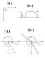
- the control state in which the automatic phase control loop described above is established when power is first applied by closing a power switch is not known. If the phase of the synchronous detection is deviated by 180° or more at the time of the establishment of the loop, stable pull-in cannot be obtained. For example, if the phase of the synchronous detection of the first demodulator 45A is in a range indicated by ⁇ ⁇ in Figure 6, where the phase range of the voltage controlled variable phase shifter 52 is indicated at 0 0 , the automatic phase control is stopped at one limit 0 LA of the range 0 0 , so that the phase can no longer be locked at the correct phase.
- the amount of phase shift by the voltage controlled variable phase shifter 52 is tentatively fixed at the center ⁇ c of the phase range as shown in Figure 7 at the time of the closure of the power switch.
- the selection switch 56 is tentatively switched to a fixed power supply 57 by a time constant circuit 58, which detects the rising of the power source voltage.
- the voltage of the fixed power supply 57 which is supplied as the control voltage to the voltage controlled variable phase shifter 52, is set to fix the phase amount to the centre 8 e .
- the selection switch 56 is switched to the level comparator 55 after the lapse of a predetermined period of time determined by the time constant circuit 58. With this switching, the voltage controlled variable phase shifter 52 in the phase control loop starts the pull-in of phase from the center 8 e .
- the synchronous detection phase thus can be automatically and reliably locked to the correct phase.
- the delayed luminance signals Y DL1 and Y DL2 respectively delayed 1 H and 2 H behind the input luminance signal Y ln for effecting the vertical contour compensation can be obtained with a single 1 H delay line 43, and the insertion loss temperature compensation of the 1 H delay line 43 is obtained through the automatic gain control function of the variable gain amplifier 44, so that the levels of the delayed luminance signals Y DL1 and Y IL2 can be automatically controlled to obtain stable regular vertical contour compensation processing.
- two delayed signals delayed by different amounts can be obtained with a simple construction utilizing a single delay line and orthogonal modulation! demodulation means.
- the orthogonally modulated signal can be reliably demodulated for steady recovery of the delayed signals through synchronous detection using the phase controlled carrier from the variable phase shifter as the synchronizing signal.
Abstract
Description
- This invention relates to delay circuit arrangements suitable for contour compensation processing of video signals.
- Video signals in video systems such as television receivers and television cameras pass through various electric circuits and signal transmission lines having finite operational frequency ranges. Therefore, attenuation of high frequency components occurs, resulting in reduction of resolution. By way of example, if the luminance signal contains a 3.58 MHz colour sub-carrier, a 35.8 MHz beat brilliance variation results in the reproduced image. To eliminate such beat interference, the video amplifier circuit in a colour television receiver has frequency characteristics such that the colour sub-carrier is attenuated by more than 15 to 16 dB. However, in such a video amplifier circuit, the high frequency components of the video signal are attenuated, resulting in reduction in the resolution of the reproduced image. In a shadow-mask type cathode ray tube, the brilliance modulation efficiency tends to be reduced when the frequency exceeds 2 MHz. Such reduction of the brilliance modulation efficiency reduces the contrast, so reducing the resolution.
- To compensate for such loss of resolution, it has been the practice to effect contour compensation processing on portions of the luminance signal waveform corresponding to the contour of the image, to produce overshoot or undershoot of 20 to 30%. This processing has the effect of increasing the sharpness of the contour portions of the image, thus improving the resolution.
- A vertical
contour compensation circuit 10 as shown in Figure 1 of the accopanying drawings has been used for improving the resolution of the image in the vertical direction thereof. - In the vertical
contour compensation circuit 10 shown in Figure 1, an input luminance signal Yln is supplied to asignal input terminal 1 to be fed to adelay line 2 and afirst adder 3. The input luminance signal Yln has a waveform as shown, for example, in Figure 2A of the accompanying drawings. Thedelay line 2 produces a first delayed luminance signal YDL, having a waveform as shown in Figure 2B of the accompanying drawings, and which is delayed relative to the input luminance signal Yln by onehorizontal scanning period 1 H, and a second delayed luminance signal YDL2 having a waveform as shown in Figure 2C of the accompanying drawings, which is delayed relative to the input luminance signal Yln by 2 H. The first delayed luminanace signal YDL1 obtained from thedelay line 2 is fed to thesubtracter 5 and asecond adder 7. The second delayed luminance signal YDL2, on the other hand, is fed to thefirst adder 3. Thefirst adder 3 adds the input luminance signal Yln and second delayed luminance signal YDL2, and feeds the resulting signal Y (having a waveform as shown in Figure 2D of the accompanying drawings) through anattenuator 4 to thesubtracter 5. Thesubtracter 5 subtracts the signal YA from the first delayed luminance signal YDL1 to obtain a contour compensation sigal SAC having a waveform as shown in Figure 2E of the accompanying drawings. This contour compensation signal SAC is fed through alevel controller 6 to thesecond adder 7. Thesecond adder 7 superimposes the contour compensation signal SAC on the first delayed luminance signal YDL1 and produces an output luminance signal Yout as shown in Figure 2F of the accompanying drawings. The signal Yout appears at anoutput terminal 8. It has a vertical contour compensated waveform with an overshoot and an undershoot resulting from the superimposition of the contour compensation signal SAC on the luminance change portions, that is, contour portions in the vertical direction of the image. - The
delay line 2 in the verticalcontour compensation circuit 10 usually uses two 1H delay lines input terminal 1 is fed to anamplitude modulator 21 in thedelay line 2 for amplitude modulation. The output of theamplitude modulator 21 is fed to thefirst delay line 22. The delayed output signal from thefirst delay line 22 is fed through a first gain controlledamplifier 23 to afirst demodulator 24. The first gain controlledamplifier 23 is gain controlled by the output of thefirst demodulator 24. The delayed output signal from thefirst delay line 22 is fed through the first gain controlledamplifier 23 to thesecond delay line 25. The delayed output signal from thesecond delay line 25 is fed through a second gain controlledamplifier 26 to asecond demodulator 27. When the input luminance signal Yln as shown in Figure 2A is fed to theamplitude modulator 21, thefirst demodulator 24 demodulates the 1 H delayed luminance signal from thefirst delay line 22 and produces the first delayed luminance signal YDL1 delayed by 1 H relative to the input luminance signal Yln as shown in Figure 2B. Thesecond demodulator 27 demodulates the luminance signal that has been delayed by 1 H in each of the first andsecond delay lines - As has been shown, the
delay line 2 in the verticalcontour compensation circuit 10 uses two 1H delay lines contour compensation circuit 10, which used twohigh performance 1 H delay lines which are required to provide a comparatively long delay time and nevertheless have wide frequency band characteristics, is inevitably very expensive, the major part of the price being accounted for by the two delay lines. Moreover, the signal level attenuation and temperature characteristics vary with invidual delay lines even of the same ratings and specifications. Therefore, where the twodelay lines amplifiers - International Broadcasting Convention, 9-13 September 1968, London, conference publication,
no 40,part 1, pages 3.16.1 to 3.16.4 discloses a delay circuit arrangement generally as the precharacterizing part ofclaim 1. - According to the present invention there is provided a delay circuit arrangement comprising:
- modulating means for effecting contour modulation of a signal using a signal from a carrier oscillator as a carrier;
- delay means for delaying the modulation output of said modulating means;
- demodulating means for effecting demodulation by synchronous detection; and
- control means;
- said demodulating means producing a first demodulated signal delayed relative to said first input signal supplied to said modulating means by an amount determined by said delay means and a second demodulated signal delayed relative to said first input signal by double said amount;
characterized by: - said delay means being a single delay device connected between said modulating means and said demodulating means;
- variable phase shifting means for phase shifting said carrier oscillator output signal;
- said demodulating means using the output of said variable phase shifting means as a synchronizing signal; and
- adding means for superimposing a reference signal in a first demodulated signal from said demodulated means corresponding to a first input signal to said modulating means and supplying the resultant signal as a second input signal to said modulating means;
- said control means controlling the amount of phase shift by said variable phase shifting means according to the reference signal demodulated by said demodulating means.
- The invention will now be described by way of example with reference to the accompanying drawings, in which:
- Figure 1 is a block diagram of a prior art vertical contour compensation circuit;
- Figure 2 shows waveforms for explaining the operation of the circuit of Figure 1;
- Figure 3 is a block diagram of an embodiment of the invention;
- Figure 4 is a vector diagram for explaining the operation of first and second amplitude modulators in the embodiment;
- Figure 5 is a waveform diagram showing an input signal to the second amplitude modulator; and
- Figures 6 and 7 are vector diagrams for explaining the operation of a voltage controlled variable phase shifter in the embodiment.
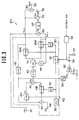
- Figure 3 is a block diagram showing an embodiment of the invention applied to a vertical contour compensation circuit.
- The illustrated vertical
contour compensation circuit 100 incorporates adelay circuit 40, which employs a single 1H delay line 43 which can provide first and second delayed luminance signals YDL1 and YDL2 respectively delayed 1 H and 2 H relative to an input luminance signal Yjn. Afirst adder 60 adds the input luminance signal Yin which is supplied to aninput terminal 30 and the second delayed luminance signal YDL2. Asubtracter 70 produces a contour compensation signal SAC from the first delayed luminance signal YDL1 and the sum signal from thefirst adder 60. Asecond adder 80 superimposes the contour compensation signal SAC on the first delayed luminance signal YDL1 to obtain a vertical contour compensated output luminance signal Yout. - The
delay circuit 40 also includes first andsecond amplitude modulators 41A and 41B for effecting so-called orthogonal modulation of a carrier from acarrier oscillator 50. The input luminance signal supplied to theinput terminal 30 is fed to thefirst amplitude modulator 41A. The carrier output signal from thecarrier oscillator 50 is supplied directly to thefirst amplitude modulator 41A, while it is supplied to the second amplitude modulator 41 B through aphase shifter 51 for shifting the phase by 90°. The orthogonal modulation is thus done withcarriers 90° out of phase with each other to produce first and second amplitude modulated components S1 and S2 which are 90° out of phase with each other as shown in the vector diagram of Figure 4, these modulated components S1 and S2 being fed to anadder 42 to be added together. The resultant sum signal SA from theadder 42 is fed through the 1H delay line 43 to a voltage controlledvariable gain amplifier 44. The 1H delay line 43 delays the sum signal SA by 1 H. The voltage controlledvariable gain amplifier 44 effects insertion loss temperature compensation of the 1 H delay line, and it is gain controlled by the output of areference signal detector 49 to be described later. The output of the voltage controlledvariable gain amplifier 44 is fed to first andsecond demodulators carrier oscillator 50 is suplied as a synchronizing signal through a voltage controlledvariable phase shifter 52 to the first andsecond demodulators variable gain amplifier 44 by synchronous detection. Aphase shifter 53 provides a phase difference of 90° between the synchronizing signals supplied to thedemodulators variable phase shifter 52 is controlled by the output of a level comparator 55 to be described later. - The
first demodulator 45A demodulates only a component of the sum signal output of the voltage controlledvariable gain amplifier 44 corresponding to the first amplitude modulation S1 by synchronous detection of the sum signal output. It recovers the first delayed luminance signal YD11 delayed 1 H relative to the input luminance signal Yin, because the sum signal output fed to it from thevariable gain amplifier 44 has been delayed 1 H through the 1H delay line 43 and the first amplitude modulated component S1 in the sum signal SA is the amplitude modulation of the input luminance signal Yln on the carrier. - The first delayed luminance signal YDL1 from the
first demodulator 45A is fed to thesubtracter 70 and thesecond adder 80 as mentioned earlier. It is further fed through aclamp circuit 46 in thedelay circuit 40 to a sample/hold circuit 54 and anadder 47. A reference signal Sφ coupled to a referencesignal input terminal 48 is fed to theadder 47 to be superimposed on the first delayed luminance signal YDL1 at a position corresponding to the blanking period as shown in Figure 5. The output of theadder 47, consisting of the reference signal Sφ and the first delayed luminance signal YDLI superimposed on each other, is fed to the second amplitude modulator 41 B. - The
second demodulator 45B, which corresponds to the second amplitude modulator 41 B, demodulates only a component of the sum signal output of the voltage controlledvariable gain amplifier 44 corresponding to the second amplitude modulated component S2, by synchronous detection of the sum signal output. It recovers the second delayed luminance signal YDL2, which is delayed 1 H relative to the first delayed luminance signal YDL1, that is, delayed 2 H relative to the input luminance signal Yln, under the control of the reference signal Sφ, because the second amplitude modulated component S2 is the amplitude modulation of the output consisting of the reference signal Sφ and the first delayed luminance signal YDL1 superimposed on each other on the carrier, and has been delayed 1 H in the 1H delay line 43 before being fed to it. - The second delayed luminance signal YDL2 is fed to the
first adder 60 for addition to the input luminance Signal Yin. The sum signal Ya from thefirst adder 60 is fed through anattenuator 65 to thesubtracter 70. Thesubtracter 70 subtracts the first delay luminance signal YDL1 and the sum signal YA one from the other to obtain the contour compensation signal SAG. Thesecond adder 80 superimposes the contour compensation signal SAC on the first delayed luminance signal YDL1, whereby the vertical contour compensated output luminance signal Yout is produced at anoutput terminal 90. - In this embodiment, a
reference signal detector 49 detects the reference signal Sφ demodulated by thesecond demodulator 45B and controls the gain of the voltage controlledvariable gain amplifier 44 to make the signal level of the reference signal Sφ constant. By this automatic gain control function, the insertion loss temperature compensation of the 1H delay line 43 is done in the voltage controlled variable gain amplifier 41 on the sum signal input thereto, that is the first and second amplitude modulation components S1 and S2, which have been delayed in the 1H delay line 43. The first andsecond demodulators variable gain amplifier 44, demodulate the first delayed luminance signal YDL1 completely free from the reference signal Sφ, so long as the phase relation of the synchronous detection, that is, the phase relation between the synchronizing signals, is correct. - In this embodiment, the output signal of the
carrier oscillator 50 is supplied as the synchronizing signal through the voltage controlledvariable phase shifter 52 to the first andsecond demodulators variable phase shifter 52 is controlled according to the output of the level comparator 55. More specifically, the level comparator 55 compares a reference voltage VREF supplied to one input terminal of it with hold voltage VSH supplied from the sample/hold circuit 54. The output representing the result of the comparison is fed through asignal selection switch 56 to the voltage controlledvariable phase shifter 52. The sample/hold circuit 54 samples and holds the output of theclamp circuit 46 at a position correponding to the reference signal Sφ superimposed on the first delayed luminance signal YDL1. The level comparator 55 compares the levels of the reference voltage VREF, which is equal in level to the clamp voltage of theclamp circuit 46, that is, the first delayed luminance signal YDL1, and the hold voltage VSH. The first delayed luminance signal YDL1, demodulated by the first demodulator does not contain any component corresponding to the second modulation component S2 of the second amplitude modulator 41B, so long as the phase of synchronous detection by thefirst demodulator 45A is correct. In other words, with the right phase of synchronous detection by thefirst demodulator 45A the first delayed luminance signal YDL1 fed to the sample/hold circuit 54 does not contain the reference signal Sφ. In this case, the clamp level is sampled and held by the sample/hold circuit 54. - It is to be understood that by controlling the amount of phase shift by the voltage controlled
variable phase shifter 52 according to the output of the level comparator 55, which compares the hold voltage VSH from the sample/hold circuit 54 with the reference voltage VREF equal to the clamped voltage, the correct phase of the synchronizing signal supplied to thefirst demodulator 45A can be maintained. Also, by feeding the synchronizing signal noted above through the 90°phase shifter 53 to thesecond demodulator 45B, the correct phase of the synchronous detection by thesecond demodulator 45B is maintained. In other words, through automatic phase control of the synchronizing signals using the voltage controlledvariable phase shifter 52, the correct phases of synchronous detection by thedemodulators H delay line 43 due to temperature changes or aging. - The control state, in which the automatic phase control loop described above is established when power is first applied by closing a power switch is not known. If the phase of the synchronous detection is deviated by 180° or more at the time of the establishment of the loop, stable pull-in cannot be obtained. For example, if the phase of the synchronous detection of the
first demodulator 45A is in a range indicated by θΔ in Figure 6, where the phase range of the voltage controlledvariable phase shifter 52 is indicated at 00, the automatic phase control is stopped at one limit 0LA of the range 00, so that the phase can no longer be locked at the correct phase. - In this embodiment, the amount of phase shift by the voltage controlled
variable phase shifter 52 is tentatively fixed at the center θc of the phase range as shown in Figure 7 at the time of the closure of the power switch. By so doing, reliable pull-in to the correct phase can be obtained. More specifically, at the time of the closure of the power switch, theselection switch 56 is tentatively switched to a fixedpower supply 57 by a timeconstant circuit 58, which detects the rising of the power source voltage. The voltage of the fixedpower supply 57, which is supplied as the control voltage to the voltage controlledvariable phase shifter 52, is set to fix the phase amount to thecentre 8e. Theselection switch 56 is switched to the level comparator 55 after the lapse of a predetermined period of time determined by the timeconstant circuit 58. With this switching, the voltage controlledvariable phase shifter 52 in the phase control loop starts the pull-in of phase from thecenter 8e. The synchronous detection phase thus can be automatically and reliably locked to the correct phase. - As has been shown, in the above embodiment the delayed luminance signals YDL1 and YDL2 respectively delayed 1 H and 2 H behind the input luminance signal Yln for effecting the vertical contour compensation can be obtained with a single 1
H delay line 43, and the insertion loss temperature compensation of the 1H delay line 43 is obtained through the automatic gain control function of thevariable gain amplifier 44, so that the levels of the delayed luminance signals YDL1 and YIL2 can be automatically controlled to obtain stable regular vertical contour compensation processing. - As has been described in the foregoing, two delayed signals delayed by different amounts can be obtained with a simple construction utilizing a single delay line and orthogonal modulation! demodulation means. Also, the orthogonally modulated signal can be reliably demodulated for steady recovery of the delayed signals through synchronous detection using the phase controlled carrier from the variable phase shifter as the synchronizing signal.
Claims (3)
characterized by:
Priority Applications (1)
| Application Number | Priority Date | Filing Date | Title |
|---|---|---|---|
| AT83304600T ATE42436T1 (en) | 1982-08-10 | 1983-08-09 | DELAY CIRCUIT ARRANGEMENTS. |
Applications Claiming Priority (2)
| Application Number | Priority Date | Filing Date | Title |
|---|---|---|---|
| JP137863/82 | 1982-08-10 | ||
| JP57137863A JPS5928766A (en) | 1982-08-10 | 1982-08-10 | Delay circuit |
Publications (3)
| Publication Number | Publication Date |
|---|---|
| EP0102773A2 EP0102773A2 (en) | 1984-03-14 |
| EP0102773A3 EP0102773A3 (en) | 1985-07-03 |
| EP0102773B1 true EP0102773B1 (en) | 1989-04-19 |
Family
ID=15208505
Family Applications (1)
| Application Number | Title | Priority Date | Filing Date |
|---|---|---|---|
| EP83304600A Expired EP0102773B1 (en) | 1982-08-10 | 1983-08-09 | Delay circuit arrangements |
Country Status (7)
| Country | Link |
|---|---|
| US (1) | US4558354A (en) |
| EP (1) | EP0102773B1 (en) |
| JP (1) | JPS5928766A (en) |
| AT (1) | ATE42436T1 (en) |
| AU (1) | AU551114B2 (en) |
| CA (1) | CA1200858A (en) |
| DE (1) | DE3379709D1 (en) |
Cited By (18)
| Publication number | Priority date | Publication date | Assignee | Title |
|---|---|---|---|---|
| US7708152B2 (en) | 2005-02-07 | 2010-05-04 | Hanuman Llc | Method and apparatus for preparing platelet rich plasma and concentrates thereof |
| US7780860B2 (en) | 2002-05-24 | 2010-08-24 | Biomet Biologics, Llc | Apparatus and method for separating and concentrating fluids containing multiple components |
| US7806276B2 (en) | 2007-04-12 | 2010-10-05 | Hanuman, Llc | Buoy suspension fractionation system |
| US7824559B2 (en) | 2005-02-07 | 2010-11-02 | Hanumann, LLC | Apparatus and method for preparing platelet rich plasma and concentrates thereof |
| US7832566B2 (en) | 2002-05-24 | 2010-11-16 | Biomet Biologics, Llc | Method and apparatus for separating and concentrating a component from a multi-component material including macroparticles |
| US7837884B2 (en) | 2002-05-03 | 2010-11-23 | Hanuman, Llc | Methods and apparatus for isolating platelets from blood |
| US7845499B2 (en) | 2002-05-24 | 2010-12-07 | Biomet Biologics, Llc | Apparatus and method for separating and concentrating fluids containing multiple components |
| US7866485B2 (en) | 2005-02-07 | 2011-01-11 | Hanuman, Llc | Apparatus and method for preparing platelet rich plasma and concentrates thereof |
| US7992725B2 (en) | 2002-05-03 | 2011-08-09 | Biomet Biologics, Llc | Buoy suspension fractionation system |
| US8012077B2 (en) | 2008-05-23 | 2011-09-06 | Biomet Biologics, Llc | Blood separating device |
| US8187475B2 (en) | 2009-03-06 | 2012-05-29 | Biomet Biologics, Llc | Method and apparatus for producing autologous thrombin |
| US8313954B2 (en) | 2009-04-03 | 2012-11-20 | Biomet Biologics, Llc | All-in-one means of separating blood components |
| US8328024B2 (en) | 2007-04-12 | 2012-12-11 | Hanuman, Llc | Buoy suspension fractionation system |
| US8337711B2 (en) | 2008-02-29 | 2012-12-25 | Biomet Biologics, Llc | System and process for separating a material |
| US8567609B2 (en) | 2006-05-25 | 2013-10-29 | Biomet Biologics, Llc | Apparatus and method for separating and concentrating fluids containing multiple components |
| US8591391B2 (en) | 2010-04-12 | 2013-11-26 | Biomet Biologics, Llc | Method and apparatus for separating a material |
| US9011800B2 (en) | 2009-07-16 | 2015-04-21 | Biomet Biologics, Llc | Method and apparatus for separating biological materials |
| US9556243B2 (en) | 2013-03-15 | 2017-01-31 | Biomet Biologies, LLC | Methods for making cytokine compositions from tissues using non-centrifugal methods |
Families Citing this family (16)
| Publication number | Priority date | Publication date | Assignee | Title |
|---|---|---|---|---|
| GB2151429B (en) * | 1983-11-26 | 1987-03-18 | Toshiba Kk | Vertical contour correction device |
| JPS60114090A (en) * | 1983-11-26 | 1985-06-20 | Toshiba Corp | Vertical contour correction device |
| KR920004441Y1 (en) * | 1989-12-30 | 1992-06-29 | 삼성전자 주식회사 | Aperture edge amount compensation circuit of video monitor |
| US5585007A (en) | 1994-12-07 | 1996-12-17 | Plasmaseal Corporation | Plasma concentrate and tissue sealant methods and apparatuses for making concentrated plasma and/or tissue sealant |
| KR100872213B1 (en) * | 2000-07-07 | 2008-12-05 | 모사이드 테크놀로지스, 인코포레이티드 | A method for performing a read command in a memory device |
| US20060278588A1 (en) | 2002-05-24 | 2006-12-14 | Woodell-May Jennifer E | Apparatus and method for separating and concentrating fluids containing multiple components |
| JP4423157B2 (en) * | 2004-10-06 | 2010-03-03 | キヤノン株式会社 | Power line communication apparatus and control method thereof |
| EP2567692B1 (en) | 2008-02-27 | 2016-04-06 | Biomet Biologics, LLC | Use of a device for obtaining interleukin-1 receptor antagonist rich solutions |
| US9642956B2 (en) | 2012-08-27 | 2017-05-09 | Biomet Biologics, Llc | Apparatus and method for separating and concentrating fluids containing multiple components |
| US20140271589A1 (en) | 2013-03-15 | 2014-09-18 | Biomet Biologics, Llc | Treatment of collagen defects using protein solutions |
| US9950035B2 (en) | 2013-03-15 | 2018-04-24 | Biomet Biologics, Llc | Methods and non-immunogenic compositions for treating inflammatory disorders |
| US9895418B2 (en) | 2013-03-15 | 2018-02-20 | Biomet Biologics, Llc | Treatment of peripheral vascular disease using protein solutions |
| US10143725B2 (en) | 2013-03-15 | 2018-12-04 | Biomet Biologics, Llc | Treatment of pain using protein solutions |
| US9713810B2 (en) | 2015-03-30 | 2017-07-25 | Biomet Biologics, Llc | Cell washing plunger using centrifugal force |
| US9757721B2 (en) | 2015-05-11 | 2017-09-12 | Biomet Biologics, Llc | Cell washing plunger using centrifugal force |
| US10171282B1 (en) * | 2017-11-09 | 2019-01-01 | Sprint Communications Company L.P. | Dynamic optimization of amplitude weights |
Family Cites Families (6)
| Publication number | Priority date | Publication date | Assignee | Title |
|---|---|---|---|---|
| NL6604020A (en) * | 1966-03-26 | 1967-09-27 | ||
| JPS5141297B1 (en) * | 1969-11-24 | 1976-11-09 | ||
| GB1353618A (en) * | 1970-08-29 | 1974-05-22 | Marconi Co Ltd | Colour television camera equipments |
| JPS54143021A (en) * | 1978-04-28 | 1979-11-07 | Sony Corp | Processing circuit of video signal |
| CA1187167A (en) * | 1981-07-09 | 1985-05-14 | Sadaaki Tanaka | Video signal processing circuit |
| JPH0230943U (en) * | 1988-08-19 | 1990-02-27 |
-
1982
- 1982-08-10 JP JP57137863A patent/JPS5928766A/en active Granted
-
1983
- 1983-08-02 AU AU17503/83A patent/AU551114B2/en not_active Ceased
- 1983-08-03 CA CA000433835A patent/CA1200858A/en not_active Expired
- 1983-08-08 US US06/521,363 patent/US4558354A/en not_active Expired - Fee Related
- 1983-08-09 EP EP83304600A patent/EP0102773B1/en not_active Expired
- 1983-08-09 DE DE8383304600T patent/DE3379709D1/en not_active Expired
- 1983-08-09 AT AT83304600T patent/ATE42436T1/en not_active IP Right Cessation
Cited By (38)
| Publication number | Priority date | Publication date | Assignee | Title |
|---|---|---|---|---|
| US7837884B2 (en) | 2002-05-03 | 2010-11-23 | Hanuman, Llc | Methods and apparatus for isolating platelets from blood |
| US8950586B2 (en) | 2002-05-03 | 2015-02-10 | Hanuman Llc | Methods and apparatus for isolating platelets from blood |
| US8187477B2 (en) | 2002-05-03 | 2012-05-29 | Hanuman, Llc | Methods and apparatus for isolating platelets from blood |
| US7992725B2 (en) | 2002-05-03 | 2011-08-09 | Biomet Biologics, Llc | Buoy suspension fractionation system |
| US8603346B2 (en) | 2002-05-24 | 2013-12-10 | Biomet Biologics, Llc | Apparatus and method for separating and concentrating fluids containing multiple components |
| US8808551B2 (en) | 2002-05-24 | 2014-08-19 | Biomet Biologics, Llc | Apparatus and method for separating and concentrating fluids containing multiple components |
| US7845499B2 (en) | 2002-05-24 | 2010-12-07 | Biomet Biologics, Llc | Apparatus and method for separating and concentrating fluids containing multiple components |
| US9114334B2 (en) | 2002-05-24 | 2015-08-25 | Biomet Biologics, Llc | Apparatus and method for separating and concentrating fluids containing multiple components |
| US7914689B2 (en) | 2002-05-24 | 2011-03-29 | Biomet Biologics, Llc | Apparatus and method for separating and concentrating fluids containing multiple components |
| US7780860B2 (en) | 2002-05-24 | 2010-08-24 | Biomet Biologics, Llc | Apparatus and method for separating and concentrating fluids containing multiple components |
| US7832566B2 (en) | 2002-05-24 | 2010-11-16 | Biomet Biologics, Llc | Method and apparatus for separating and concentrating a component from a multi-component material including macroparticles |
| US8163184B2 (en) | 2002-05-24 | 2012-04-24 | Biomet Biologics, Llc | Apparatus and method for separating and concentrating fluids containing multiple components |
| US8048321B2 (en) | 2002-05-24 | 2011-11-01 | Biomet Biologics, Llc | Apparatus and method for separating and concentrating fluids containing multiple components |
| US8062534B2 (en) | 2002-05-24 | 2011-11-22 | Biomet Biologics, Llc | Apparatus and method for separating and concentrating fluids containing multiple components |
| US8096422B2 (en) | 2005-02-07 | 2012-01-17 | Hanuman Llc | Apparatus and method for preparing platelet rich plasma and concentrates thereof |
| US7824559B2 (en) | 2005-02-07 | 2010-11-02 | Hanumann, LLC | Apparatus and method for preparing platelet rich plasma and concentrates thereof |
| US7987995B2 (en) | 2005-02-07 | 2011-08-02 | Hanuman, Llc | Method and apparatus for preparing platelet rich plasma and concentrates thereof |
| US8133389B2 (en) | 2005-02-07 | 2012-03-13 | Hanuman, Llc | Method and apparatus for preparing platelet rich plasma and concentrates thereof |
| US7708152B2 (en) | 2005-02-07 | 2010-05-04 | Hanuman Llc | Method and apparatus for preparing platelet rich plasma and concentrates thereof |
| US7866485B2 (en) | 2005-02-07 | 2011-01-11 | Hanuman, Llc | Apparatus and method for preparing platelet rich plasma and concentrates thereof |
| US8105495B2 (en) | 2005-02-07 | 2012-01-31 | Hanuman, Llc | Method for preparing platelet rich plasma and concentrates thereof |
| US8567609B2 (en) | 2006-05-25 | 2013-10-29 | Biomet Biologics, Llc | Apparatus and method for separating and concentrating fluids containing multiple components |
| US8328024B2 (en) | 2007-04-12 | 2012-12-11 | Hanuman, Llc | Buoy suspension fractionation system |
| US9138664B2 (en) | 2007-04-12 | 2015-09-22 | Biomet Biologics, Llc | Buoy fractionation system |
| US7806276B2 (en) | 2007-04-12 | 2010-10-05 | Hanuman, Llc | Buoy suspension fractionation system |
| US8596470B2 (en) | 2007-04-12 | 2013-12-03 | Hanuman, Llc | Buoy fractionation system |
| US8119013B2 (en) | 2007-04-12 | 2012-02-21 | Hanuman, Llc | Method of separating a selected component from a multiple component material |
| US8337711B2 (en) | 2008-02-29 | 2012-12-25 | Biomet Biologics, Llc | System and process for separating a material |
| US8012077B2 (en) | 2008-05-23 | 2011-09-06 | Biomet Biologics, Llc | Blood separating device |
| US8187475B2 (en) | 2009-03-06 | 2012-05-29 | Biomet Biologics, Llc | Method and apparatus for producing autologous thrombin |
| US8783470B2 (en) | 2009-03-06 | 2014-07-22 | Biomet Biologics, Llc | Method and apparatus for producing autologous thrombin |
| US8992862B2 (en) | 2009-04-03 | 2015-03-31 | Biomet Biologics, Llc | All-in-one means of separating blood components |
| US8313954B2 (en) | 2009-04-03 | 2012-11-20 | Biomet Biologics, Llc | All-in-one means of separating blood components |
| US9011800B2 (en) | 2009-07-16 | 2015-04-21 | Biomet Biologics, Llc | Method and apparatus for separating biological materials |
| US8591391B2 (en) | 2010-04-12 | 2013-11-26 | Biomet Biologics, Llc | Method and apparatus for separating a material |
| US9533090B2 (en) | 2010-04-12 | 2017-01-03 | Biomet Biologics, Llc | Method and apparatus for separating a material |
| US9239276B2 (en) | 2011-04-19 | 2016-01-19 | Biomet Biologics, Llc | Apparatus and method for separating and concentrating fluids containing multiple components |
| US9556243B2 (en) | 2013-03-15 | 2017-01-31 | Biomet Biologies, LLC | Methods for making cytokine compositions from tissues using non-centrifugal methods |
Also Published As
| Publication number | Publication date |
|---|---|
| EP0102773A2 (en) | 1984-03-14 |
| DE3379709D1 (en) | 1989-05-24 |
| ATE42436T1 (en) | 1989-05-15 |
| JPH0430230B2 (en) | 1992-05-21 |
| CA1200858A (en) | 1986-02-18 |
| AU1750383A (en) | 1984-02-16 |
| AU551114B2 (en) | 1986-04-17 |
| US4558354A (en) | 1985-12-10 |
| EP0102773A3 (en) | 1985-07-03 |
| JPS5928766A (en) | 1984-02-15 |
Similar Documents
| Publication | Publication Date | Title |
|---|---|---|
| EP0102773B1 (en) | Delay circuit arrangements | |
| US5940572A (en) | Integrated television and video cassette recorder system | |
| US4514763A (en) | Sound signal and impulse noise detector for television receivers | |
| US4434438A (en) | Low cost automatic equalizer | |
| US4306247A (en) | Color signal controlling apparatus | |
| US4285006A (en) | Ghost cancellation circuit system | |
| US4400742A (en) | Magnetic recording and reproducing apparatus for color video signals | |
| JPH0638230A (en) | Skin color correction and its device | |
| US4081837A (en) | Undesired signal canceller | |
| US4481537A (en) | Aperture correction circuit | |
| US5255076A (en) | Flesh correction circuit and method of flesh correction | |
| EP0160531B1 (en) | Demodulator circuits for amplitude-modulated signals | |
| CA2071283C (en) | Satellite television broadcasting receiver | |
| KR100203373B1 (en) | Video signal decoding apparatus | |
| KR100406451B1 (en) | Signal processing circuit | |
| CA1085043A (en) | Still color television signal recording and reproducing apparatus | |
| KR100462534B1 (en) | Frequency conversion circuit of color signal | |
| US4654601A (en) | Demodulator for television signals with feedback to correlate frames or lines | |
| KR920002840B1 (en) | Tv sound detection system | |
| EP0221254A2 (en) | Color tone adjusting device | |
| JPH0230943Y2 (en) | ||
| CA1212464A (en) | Television sound detection system using a frequency translation phase-locked loop | |
| KR100199311B1 (en) | The chroma signal processing circuit | |
| JPS5928765A (en) | Vertical profile correcting circuit | |
| JPS589474A (en) | Delaying circuit |
Legal Events
| Date | Code | Title | Description |
|---|---|---|---|
| PUAI | Public reference made under article 153(3) epc to a published international application that has entered the european phase |
Free format text: ORIGINAL CODE: 0009012 |
|
| AK | Designated contracting states |
Designated state(s): AT DE FR GB NL |
|
| PUAL | Search report despatched |
Free format text: ORIGINAL CODE: 0009013 |
|
| AK | Designated contracting states |
Designated state(s): AT DE FR GB NL |
|
| 17P | Request for examination filed |
Effective date: 19851119 |
|
| 17Q | First examination report despatched |
Effective date: 19871117 |
|
| GRAA | (expected) grant |
Free format text: ORIGINAL CODE: 0009210 |
|
| AK | Designated contracting states |
Kind code of ref document: B1 Designated state(s): AT DE FR GB NL |
|
| REF | Corresponds to: |
Ref document number: 42436 Country of ref document: AT Date of ref document: 19890515 Kind code of ref document: T |
|
| REF | Corresponds to: |
Ref document number: 3379709 Country of ref document: DE Date of ref document: 19890524 |
|
| ET | Fr: translation filed | ||
| PLBE | No opposition filed within time limit |
Free format text: ORIGINAL CODE: 0009261 |
|
| STAA | Information on the status of an ep patent application or granted ep patent |
Free format text: STATUS: NO OPPOSITION FILED WITHIN TIME LIMIT |
|
| 26N | No opposition filed | ||
| PGFP | Annual fee paid to national office [announced via postgrant information from national office to epo] |
Ref country code: GB Payment date: 19930806 Year of fee payment: 11 |
|
| PGFP | Annual fee paid to national office [announced via postgrant information from national office to epo] |
Ref country code: AT Payment date: 19930826 Year of fee payment: 11 |
|
| PGFP | Annual fee paid to national office [announced via postgrant information from national office to epo] |
Ref country code: FR Payment date: 19930827 Year of fee payment: 11 |
|
| PGFP | Annual fee paid to national office [announced via postgrant information from national office to epo] |
Ref country code: NL Payment date: 19930831 Year of fee payment: 11 |
|
| PGFP | Annual fee paid to national office [announced via postgrant information from national office to epo] |
Ref country code: DE Payment date: 19931029 Year of fee payment: 11 |
|
| PG25 | Lapsed in a contracting state [announced via postgrant information from national office to epo] |
Ref country code: GB Effective date: 19940809 Ref country code: AT Effective date: 19940809 |
|
| PG25 | Lapsed in a contracting state [announced via postgrant information from national office to epo] |
Ref country code: NL Effective date: 19950301 |
|
| GBPC | Gb: european patent ceased through non-payment of renewal fee |
Effective date: 19940809 |
|
| NLV4 | Nl: lapsed or anulled due to non-payment of the annual fee | ||
| PG25 | Lapsed in a contracting state [announced via postgrant information from national office to epo] |
Ref country code: FR Effective date: 19950428 |
|
| PG25 | Lapsed in a contracting state [announced via postgrant information from national office to epo] |
Ref country code: DE Effective date: 19950503 |
|
| REG | Reference to a national code |
Ref country code: FR Ref legal event code: ST |