EP0146181A2 - Semiconductor device comprising a combined bipolar-field effect transistor - Google Patents
Semiconductor device comprising a combined bipolar-field effect transistor Download PDFInfo
- Publication number
- EP0146181A2 EP0146181A2 EP84201803A EP84201803A EP0146181A2 EP 0146181 A2 EP0146181 A2 EP 0146181A2 EP 84201803 A EP84201803 A EP 84201803A EP 84201803 A EP84201803 A EP 84201803A EP 0146181 A2 EP0146181 A2 EP 0146181A2
- Authority
- EP
- European Patent Office
- Prior art keywords
- region
- conductivity type
- layer
- field effect
- effect transistor
- Prior art date
- Legal status (The legal status is an assumption and is not a legal conclusion. Google has not performed a legal analysis and makes no representation as to the accuracy of the status listed.)
- Granted
Links
- 230000000694 effects Effects 0.000 title claims abstract description 32
- 239000004065 semiconductor Substances 0.000 title claims abstract description 8
- 239000010410 layer Substances 0.000 claims abstract description 66
- 239000000758 substrate Substances 0.000 claims abstract description 35
- 239000002344 surface layer Substances 0.000 claims abstract description 31
- 238000000034 method Methods 0.000 claims abstract description 7
- 230000005669 field effect Effects 0.000 claims description 9
- 238000002955 isolation Methods 0.000 abstract description 6
- 239000000969 carrier Substances 0.000 description 7
- 230000015556 catabolic process Effects 0.000 description 7
- 230000001965 increasing effect Effects 0.000 description 5
- 238000013461 design Methods 0.000 description 3
- VYPSYNLAJGMNEJ-UHFFFAOYSA-N Silicium dioxide Chemical compound O=[Si]=O VYPSYNLAJGMNEJ-UHFFFAOYSA-N 0.000 description 2
- 230000004888 barrier function Effects 0.000 description 2
- 230000005684 electric field Effects 0.000 description 2
- 230000002708 enhancing effect Effects 0.000 description 2
- 238000010348 incorporation Methods 0.000 description 2
- 238000002347 injection Methods 0.000 description 2
- 239000007924 injection Substances 0.000 description 2
- 238000004519 manufacturing process Methods 0.000 description 2
- 239000000463 material Substances 0.000 description 2
- 238000005215 recombination Methods 0.000 description 2
- 230000006798 recombination Effects 0.000 description 2
- 238000012360 testing method Methods 0.000 description 2
- 238000006677 Appel reaction Methods 0.000 description 1
- 230000000903 blocking effect Effects 0.000 description 1
- 238000006243 chemical reaction Methods 0.000 description 1
- 230000002301 combined effect Effects 0.000 description 1
- 238000010276 construction Methods 0.000 description 1
- 230000003247 decreasing effect Effects 0.000 description 1
- 239000011810 insulating material Substances 0.000 description 1
- 230000010354 integration Effects 0.000 description 1
- 238000012856 packing Methods 0.000 description 1
- 238000007493 shaping process Methods 0.000 description 1
- 235000012239 silicon dioxide Nutrition 0.000 description 1
- 239000000377 silicon dioxide Substances 0.000 description 1
Images

Classifications
-
- H—ELECTRICITY
- H01—ELECTRIC ELEMENTS
- H01L—SEMICONDUCTOR DEVICES NOT COVERED BY CLASS H10
- H01L29/00—Semiconductor devices adapted for rectifying, amplifying, oscillating or switching, or capacitors or resistors with at least one potential-jump barrier or surface barrier, e.g. PN junction depletion layer or carrier concentration layer; Details of semiconductor bodies or of electrodes thereof ; Multistep manufacturing processes therefor
- H01L29/66—Types of semiconductor device ; Multistep manufacturing processes therefor
- H01L29/68—Types of semiconductor device ; Multistep manufacturing processes therefor controllable by only the electric current supplied, or only the electric potential applied, to an electrode which does not carry the current to be rectified, amplified or switched
- H01L29/76—Unipolar devices, e.g. field effect transistors
- H01L29/772—Field effect transistors
- H01L29/78—Field effect transistors with field effect produced by an insulated gate
- H01L29/7801—DMOS transistors, i.e. MISFETs with a channel accommodating body or base region adjoining a drain drift region
- H01L29/7816—Lateral DMOS transistors, i.e. LDMOS transistors
-
- H—ELECTRICITY
- H01—ELECTRIC ELEMENTS
- H01L—SEMICONDUCTOR DEVICES NOT COVERED BY CLASS H10
- H01L21/00—Processes or apparatus adapted for the manufacture or treatment of semiconductor or solid state devices or of parts thereof
- H01L21/70—Manufacture or treatment of devices consisting of a plurality of solid state components formed in or on a common substrate or of parts thereof; Manufacture of integrated circuit devices or of parts thereof
- H01L21/71—Manufacture of specific parts of devices defined in group H01L21/70
- H01L21/74—Making of localized buried regions, e.g. buried collector layers, internal connections substrate contacts
-
- H—ELECTRICITY
- H01—ELECTRIC ELEMENTS
- H01L—SEMICONDUCTOR DEVICES NOT COVERED BY CLASS H10
- H01L27/00—Devices consisting of a plurality of semiconductor or other solid-state components formed in or on a common substrate
- H01L27/02—Devices consisting of a plurality of semiconductor or other solid-state components formed in or on a common substrate including semiconductor components specially adapted for rectifying, oscillating, amplifying or switching and having at least one potential-jump barrier or surface barrier; including integrated passive circuit elements with at least one potential-jump barrier or surface barrier
- H01L27/04—Devices consisting of a plurality of semiconductor or other solid-state components formed in or on a common substrate including semiconductor components specially adapted for rectifying, oscillating, amplifying or switching and having at least one potential-jump barrier or surface barrier; including integrated passive circuit elements with at least one potential-jump barrier or surface barrier the substrate being a semiconductor body
- H01L27/06—Devices consisting of a plurality of semiconductor or other solid-state components formed in or on a common substrate including semiconductor components specially adapted for rectifying, oscillating, amplifying or switching and having at least one potential-jump barrier or surface barrier; including integrated passive circuit elements with at least one potential-jump barrier or surface barrier the substrate being a semiconductor body including a plurality of individual components in a non-repetitive configuration
- H01L27/07—Devices consisting of a plurality of semiconductor or other solid-state components formed in or on a common substrate including semiconductor components specially adapted for rectifying, oscillating, amplifying or switching and having at least one potential-jump barrier or surface barrier; including integrated passive circuit elements with at least one potential-jump barrier or surface barrier the substrate being a semiconductor body including a plurality of individual components in a non-repetitive configuration the components having an active region in common
- H01L27/0705—Devices consisting of a plurality of semiconductor or other solid-state components formed in or on a common substrate including semiconductor components specially adapted for rectifying, oscillating, amplifying or switching and having at least one potential-jump barrier or surface barrier; including integrated passive circuit elements with at least one potential-jump barrier or surface barrier the substrate being a semiconductor body including a plurality of individual components in a non-repetitive configuration the components having an active region in common comprising components of the field effect type
- H01L27/0711—Devices consisting of a plurality of semiconductor or other solid-state components formed in or on a common substrate including semiconductor components specially adapted for rectifying, oscillating, amplifying or switching and having at least one potential-jump barrier or surface barrier; including integrated passive circuit elements with at least one potential-jump barrier or surface barrier the substrate being a semiconductor body including a plurality of individual components in a non-repetitive configuration the components having an active region in common comprising components of the field effect type in combination with bipolar transistors and diodes, or capacitors, or resistors
- H01L27/0716—Devices consisting of a plurality of semiconductor or other solid-state components formed in or on a common substrate including semiconductor components specially adapted for rectifying, oscillating, amplifying or switching and having at least one potential-jump barrier or surface barrier; including integrated passive circuit elements with at least one potential-jump barrier or surface barrier the substrate being a semiconductor body including a plurality of individual components in a non-repetitive configuration the components having an active region in common comprising components of the field effect type in combination with bipolar transistors and diodes, or capacitors, or resistors in combination with vertical bipolar transistors and diodes, or capacitors, or resistors
-
- H—ELECTRICITY
- H01—ELECTRIC ELEMENTS
- H01L—SEMICONDUCTOR DEVICES NOT COVERED BY CLASS H10
- H01L29/00—Semiconductor devices adapted for rectifying, amplifying, oscillating or switching, or capacitors or resistors with at least one potential-jump barrier or surface barrier, e.g. PN junction depletion layer or carrier concentration layer; Details of semiconductor bodies or of electrodes thereof ; Multistep manufacturing processes therefor
- H01L29/02—Semiconductor bodies ; Multistep manufacturing processes therefor
- H01L29/06—Semiconductor bodies ; Multistep manufacturing processes therefor characterised by their shape; characterised by the shapes, relative sizes, or dispositions of the semiconductor regions ; characterised by the concentration or distribution of impurities within semiconductor regions
- H01L29/0603—Semiconductor bodies ; Multistep manufacturing processes therefor characterised by their shape; characterised by the shapes, relative sizes, or dispositions of the semiconductor regions ; characterised by the concentration or distribution of impurities within semiconductor regions characterised by particular constructional design considerations, e.g. for preventing surface leakage, for controlling electric field concentration or for internal isolations regions
- H01L29/0607—Semiconductor bodies ; Multistep manufacturing processes therefor characterised by their shape; characterised by the shapes, relative sizes, or dispositions of the semiconductor regions ; characterised by the concentration or distribution of impurities within semiconductor regions characterised by particular constructional design considerations, e.g. for preventing surface leakage, for controlling electric field concentration or for internal isolations regions for preventing surface leakage or controlling electric field concentration
- H01L29/0611—Semiconductor bodies ; Multistep manufacturing processes therefor characterised by their shape; characterised by the shapes, relative sizes, or dispositions of the semiconductor regions ; characterised by the concentration or distribution of impurities within semiconductor regions characterised by particular constructional design considerations, e.g. for preventing surface leakage, for controlling electric field concentration or for internal isolations regions for preventing surface leakage or controlling electric field concentration for increasing or controlling the breakdown voltage of reverse biased devices
- H01L29/0615—Semiconductor bodies ; Multistep manufacturing processes therefor characterised by their shape; characterised by the shapes, relative sizes, or dispositions of the semiconductor regions ; characterised by the concentration or distribution of impurities within semiconductor regions characterised by particular constructional design considerations, e.g. for preventing surface leakage, for controlling electric field concentration or for internal isolations regions for preventing surface leakage or controlling electric field concentration for increasing or controlling the breakdown voltage of reverse biased devices by the doping profile or the shape or the arrangement of the PN junction, or with supplementary regions, e.g. junction termination extension [JTE]
- H01L29/0619—Semiconductor bodies ; Multistep manufacturing processes therefor characterised by their shape; characterised by the shapes, relative sizes, or dispositions of the semiconductor regions ; characterised by the concentration or distribution of impurities within semiconductor regions characterised by particular constructional design considerations, e.g. for preventing surface leakage, for controlling electric field concentration or for internal isolations regions for preventing surface leakage or controlling electric field concentration for increasing or controlling the breakdown voltage of reverse biased devices by the doping profile or the shape or the arrangement of the PN junction, or with supplementary regions, e.g. junction termination extension [JTE] with a supplementary region doped oppositely to or in rectifying contact with the semiconductor containing or contacting region, e.g. guard rings with PN or Schottky junction
-
- H—ELECTRICITY
- H01—ELECTRIC ELEMENTS
- H01L—SEMICONDUCTOR DEVICES NOT COVERED BY CLASS H10
- H01L29/00—Semiconductor devices adapted for rectifying, amplifying, oscillating or switching, or capacitors or resistors with at least one potential-jump barrier or surface barrier, e.g. PN junction depletion layer or carrier concentration layer; Details of semiconductor bodies or of electrodes thereof ; Multistep manufacturing processes therefor
- H01L29/66—Types of semiconductor device ; Multistep manufacturing processes therefor
- H01L29/68—Types of semiconductor device ; Multistep manufacturing processes therefor controllable by only the electric current supplied, or only the electric potential applied, to an electrode which does not carry the current to be rectified, amplified or switched
- H01L29/70—Bipolar devices
- H01L29/72—Transistor-type devices, i.e. able to continuously respond to applied control signals
- H01L29/73—Bipolar junction transistors
- H01L29/7302—Bipolar junction transistors structurally associated with other devices
-
- H—ELECTRICITY
- H01—ELECTRIC ELEMENTS
- H01L—SEMICONDUCTOR DEVICES NOT COVERED BY CLASS H10
- H01L29/00—Semiconductor devices adapted for rectifying, amplifying, oscillating or switching, or capacitors or resistors with at least one potential-jump barrier or surface barrier, e.g. PN junction depletion layer or carrier concentration layer; Details of semiconductor bodies or of electrodes thereof ; Multistep manufacturing processes therefor
- H01L29/66—Types of semiconductor device ; Multistep manufacturing processes therefor
- H01L29/68—Types of semiconductor device ; Multistep manufacturing processes therefor controllable by only the electric current supplied, or only the electric potential applied, to an electrode which does not carry the current to be rectified, amplified or switched
- H01L29/70—Bipolar devices
- H01L29/72—Transistor-type devices, i.e. able to continuously respond to applied control signals
- H01L29/739—Transistor-type devices, i.e. able to continuously respond to applied control signals controlled by field-effect, e.g. bipolar static induction transistors [BSIT]
- H01L29/7393—Insulated gate bipolar mode transistors, i.e. IGBT; IGT; COMFET
-
- H—ELECTRICITY
- H01—ELECTRIC ELEMENTS
- H01L—SEMICONDUCTOR DEVICES NOT COVERED BY CLASS H10
- H01L29/00—Semiconductor devices adapted for rectifying, amplifying, oscillating or switching, or capacitors or resistors with at least one potential-jump barrier or surface barrier, e.g. PN junction depletion layer or carrier concentration layer; Details of semiconductor bodies or of electrodes thereof ; Multistep manufacturing processes therefor
- H01L29/02—Semiconductor bodies ; Multistep manufacturing processes therefor
- H01L29/06—Semiconductor bodies ; Multistep manufacturing processes therefor characterised by their shape; characterised by the shapes, relative sizes, or dispositions of the semiconductor regions ; characterised by the concentration or distribution of impurities within semiconductor regions
- H01L29/08—Semiconductor bodies ; Multistep manufacturing processes therefor characterised by their shape; characterised by the shapes, relative sizes, or dispositions of the semiconductor regions ; characterised by the concentration or distribution of impurities within semiconductor regions with semiconductor regions connected to an electrode carrying current to be rectified, amplified or switched and such electrode being part of a semiconductor device which comprises three or more electrodes
- H01L29/0843—Source or drain regions of field-effect devices
- H01L29/0847—Source or drain regions of field-effect devices of field-effect transistors with insulated gate
- H01L29/0852—Source or drain regions of field-effect devices of field-effect transistors with insulated gate of DMOS transistors
- H01L29/0873—Drain regions
- H01L29/0878—Impurity concentration or distribution
-
- H—ELECTRICITY
- H01—ELECTRIC ELEMENTS
- H01L—SEMICONDUCTOR DEVICES NOT COVERED BY CLASS H10
- H01L29/00—Semiconductor devices adapted for rectifying, amplifying, oscillating or switching, or capacitors or resistors with at least one potential-jump barrier or surface barrier, e.g. PN junction depletion layer or carrier concentration layer; Details of semiconductor bodies or of electrodes thereof ; Multistep manufacturing processes therefor
- H01L29/02—Semiconductor bodies ; Multistep manufacturing processes therefor
- H01L29/06—Semiconductor bodies ; Multistep manufacturing processes therefor characterised by their shape; characterised by the shapes, relative sizes, or dispositions of the semiconductor regions ; characterised by the concentration or distribution of impurities within semiconductor regions
- H01L29/10—Semiconductor bodies ; Multistep manufacturing processes therefor characterised by their shape; characterised by the shapes, relative sizes, or dispositions of the semiconductor regions ; characterised by the concentration or distribution of impurities within semiconductor regions with semiconductor regions connected to an electrode not carrying current to be rectified, amplified or switched and such electrode being part of a semiconductor device which comprises three or more electrodes
- H01L29/107—Substrate region of field-effect devices
- H01L29/1075—Substrate region of field-effect devices of field-effect transistors
- H01L29/1079—Substrate region of field-effect devices of field-effect transistors with insulated gate
- H01L29/1083—Substrate region of field-effect devices of field-effect transistors with insulated gate with an inactive supplementary region, e.g. for preventing punch-through, improving capacity effect or leakage current
Abstract
Description
- The invention relates to a combined bipolar-field effect transistor RESURF device, comprising
- a semiconductor substrate of a first conductivity type and having a major surface and a substrate electrode connected to the side of said substrate opposite said major surface,
- an epitaxial surface layer of a second conductivity type opposite to that of said first conductivity type, the doping concentration and thickness of said epitaxial surface layer being selected in accordance with the REduced SURface Field (RESURF) technique,
- a surface-adjoining base region of said first conductivity type in said epitaxial surface layer, a base electrode connected to said base region,
- a surface-adjoining source/emitter region of said second conductivity type in said base region, the source/emitter region serving both as the source and the emitter of said combined device,
- a source/emitter electrode connected to said source/emitter region,
- a surface-adjoining drain/collector region of said second conductivity type in said epitaxial surface layer and spaced apart from said base region, the drain/collector region serving as both the drain and the collector of said combined device,
- a drain/collector electrode connected to said drain/collector region,
- a surface-adjoining channel region at least partly in that portion of said base region which is adjacent said drain/collector region,
- an insulating layer on said surface layer and covering at least that part of said channel region which is in said base region and
- a gate electrode on said insulating layer and over at least that part of said channel region which is in said base region,
- Such a device is known from U.S. Patent No. 4,300,150.
- The general concept of combining bipolar and field effect transistors in a single device is well-known in the art. For example, combined bipolar-junction field effect transistor devices are shown in U.S. Patent No. 4,095,252 and IBM Technical Disclosure Bulletin, Vol. 19, No. 11, April 1977, P. 4191-4192. Additionally, a combined vertical bipolar-DMOS device is shown in U.S. Patent No. 4,344,081. Generally speaking, when such devices are used for high- power switching applications, a bipolar transistor and a field effect transistor are combined in order to achieve a single integrated device which features both the faster switching response of the field effect transistor and the lower on-resistance of the bipolar transistor.
- In order to achieve a higher level of performance in such devices, an ongoing effort has been made to improve the breakdown and switching characteristics of the devices. For example, it has been found that the breakdown characteristics of high-voltage semiconductor devices generally can be improved by using the REduced SURface Field (or RESURF) technique, as described in "High Voltage Thin Layer Devices (RESURF Devices)", "International Electronic Devices Meeting Technical Digest", December, 1979, pages 238-240, by Appels et al, and U.S. Patent No. 4,292,642, incorporated herein by reference. Essentially, the improved breakdown characteristics of RESURF devices are achieved by employing thinner but more highly doped epitaxial surface layers to reduce surface fields.
- The RESURF technique was applied to lateral double-diffused MOS transistors, as described in U.S. Patent 4,300,150 and also in "Lateral DMOS Power Transistor Design", "IEEE Electron Device Letters", Vol. EDL-1, pages 51-53, April 1980, by Colak et al, and the result was a substantial improvement in device characteristics. In high-voltage DMOS devices, there is normally a trade-off between breakdown voltage and on-resistance, with the goal being to increase the breakdown voltage level while maintaining a relatively low on-resistance. Using the RESURF technique, and for reference assuming a constant breakdown voltage, an improvement (e.g. decrease) in on-resistance by a factor of about 3 may be obtained in a device occupying the same area as a conventional (thick epitaxial layer) DMOS device. Nevertheless, a further improvement in the on-resistance and switching characteristics of such devices would be extremely desirable, particularly for high-voltage power switching devices where such characteristics are of considerable importance. Additionally, for combined bipolar-field effect transistor devices using the RESURF principle, it would be desirable to improve the manufacturing yield and minimize the area occupied by the device for a given set of switching, high-voltage, and on-resistance characteristics.
- It is therefore an object of the present invention to provide a combined bipolar-field effect transistor RESURF device having improved on-resistance and switching characteristics, while requiring a reduced amount of base drive current for a desired level of on-resistance and having a reduced amount of unwanted internal power dissipation.
- It is a further object of the invention to provide a combined bipolar-field effect transistor RESURF device in which the manufacturing yield is improved and the area occupied by the device is minimized for a given set of switching, high-voltage, and on-resistance characteristics, and in which both isolation and switching speed are improved.
- In accordance with the invention a combined bipolar-field effect transistor RESURF device as described in the preamble is characterized in that the device comprises a lightly-doped epitaxial 'buried layer of said first conductivity type on said major surface of the substrate and having a doping level at least an order of magnitude less than that of said substrate.
- In such a device, the improved on-resistance and switching characteristics mentioned above are achieved by using minority carriers for conductivity modulation, by exploiting the vertical base widening phenomenon, and by using a double-epi construction to confine minority carriers. These improvements are made possible by the incorporation of the lightly-doped epitaxial buried layer, which is located between the substrate and the epitaxial surface layer of the device.
- According to an important preferred embodiment the device according to the invention comprises a highly-doped buried region of said second conductivity type located beneath said base region and sandwiched between said epitaxial buried layer of the first conductivity type and said epitaxial surface layer of the second conductivity type. Such a highly-doped buried region reduces the base drive current and the internal power dissipation of the device.
- Devices in accordance with the invention may also include a buried annular region of the first conductivity type around and in contact with the highly-doped buried region, as well as a surface-adjoining annular region of the first conductivity type adjacent the base region.
- The various embodiments described above may additionally include a highly-doped buried layer, of the same conductivity type as that of the substrate, located in the substrate at its intersection with the lightly-doped epitaxial buried layer. This highly-doped buried layer serves to increase conductivity modulation in the lightly-doped epitaxial buried layer and also to enhance confinement of carriers to the lightly-doped epitaxial buried layer.
- Such devices not only require reduced base drive for a given level of on-resistance and provide reduced internal power dissipation, but also provide improved isolation with respect to adjacent devices on the same substrate and improved switching speed.
-
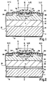
- Fig. 1 is a cross-sectional view of a combined bipolar-field effect transistor RESURF device in accordance with a first embodiment of the invention; and
- Fig. 2 is a cross-sectional view of a combined bipolar-field effect transistor RESURF device in accordance with a second embodiment of the invention.
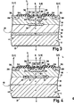
- Fig. 3 is a cross-sectional view of a combined bipolar-field effect transistor RESURF device in accordance with a third embodiment of the invention;
- Fig. 4 is a cross-sectional view of a combined bipolar-field effect transistor RESURF device in accordance with a fourth embodiment of the invention; and
- Fig. 5 is a cross-sectional view of a combined bipolar-field effect transistor RESURF device in accordance with a fifth embodiment of the invention.
- Fig. 1 of the drawing shows a combined bipolar-field effect transistor RESURF device which is suitable for high-voltage switching applications. It should be noted that the drawing is not to scale, and in particular that the vertical dimensions are exaggerated for improved clarity. Additionally, like parts are designated with like reference numerals in the figures, and semiconductor regions of the same conductivity type are shown hatched in the same direction.
- In Fig. 1, a combined bipolar-field effect
transistor RESURF device 10 has a semiconductor substrate 11 with amajor surface 12 on its upper side and asubstrate electrode 13 on its lower side. In this example the substrate 11 is of p conductivity type and has a doping level of at least about 3x10¹⁵ atoms/em3. A lightly-doped epitaxial buriedlayer 16 is located onsurface 12 of the substrate and has a doping level of at least an order of magnitude (a factor of 10 times) less than that of the substrate. The lightly-doped epitaxial buried layer here is of π (i.e. p-) conductivity type with a doping level of about 3x10¹⁴ atoms/cm and a thickness of about 30 microns. Anepitaxial surface layer 18 of n conductivity type is located on theupper surface 17 ofπ layer 16, and has a doping concentration N and thickness d selected in accordance with the REduced SURface Field (RESURF) technique, meaning that the total doping concentration per unit area of the layer (Nxd) is of the order of about 1012 atoms per square cm. In this example, theepitaxial surface layer 18 has a doping level of about 1015 atoms/cm3 and a thickness of about 10 microns. - The active regions of the combined bipolar-field effect transistor RESURF device are formed at the upper surface of
epitaxial surface layer 18. A surface-adjoiningbase region 20 of p conductivity type and a doping level of about 1017 atoms/cm3 is provided with abase electrode 22 and a surface-adjoining source/emitter region 24 of n+ conductivity type semiconductor material, withregion 24 serving as both the source and the emitter of the combined bipolar-field effect transistor device.Region 24 is provided with a source/emitter electrode 26 connected to the upper surface of the region. - A drain/
collector region 28 of n+ conductivity type is provided adjacent the surface of theepitaxial surface layer 18 and is spaced apart from thebase region 20, with a drain/collector electrode 30 connected to the upper surface of the drain/collector region. Thus a lateral npn bipolar transistor is integrally formed with a lateral MOS field effect transistor. - A surface-adjoining
channel region 32 is located between source/emitter region 24 and drain/collector region 28, and is at least partly located in that portion of the base region which is adjacent to the drain/collector region. This latter-mentioned portion of thechannel region 24 is covered by aninsulating layer 34 of a material such as silicon dioxide or other suitable insulating material, with agate electrode 36 being provided on theinsulating layer 34 and over at least that part of the channel region which is in thebase region 20. Since the various active regions of the device described above are formed in a conventional manner, they will not be discussed in further detail. - The improved operational features of the present invention are achieved by using minority carriers for conductivity modulation and by exploiting the vertical base widening phenomenon typical of lateral RESURF devices to obtain lower specific on-resistances and increased yield for a given current and voltage rating. Additionally, the configuration of this device does not compromise the attributes of low input capacitance and ease of integration which are characteristic of devices of this general type.
- In the device of Fig. 1, the-
jf layer 16 serves as the substrate for purposes of blocking voltage, and, during the "off" state, this layer is fully depleted. When the device of Fig. 1 is turned "on", a vertical pnp transistor is formed from regions of p layers 11 and 16,n layer 18 andp region 20. In the "on" state, layers 16 and 18 will be conductivity modulated by minority carriers. - To turn the device of Fig. 1 "on", base and gate drive signals are applied to
electrodes - When the doping level of
layer 16 is appropriately selected with respect to that of the underlying substrate, a potential will develop across these layers, even at a relatively low base current. If the potential drop becomes comparable to the built-in potential of the collector-base junction of the vertical pnp transistor, this transistor will also saturate. At this point, electrons will be injected from theepitaxial surface layer 18 into the highlyresistive layer 16, effectively widening the base of the vertical pnp transistor. Due to the relatively small electric fields inlayer 16, the base widening phenomenon spreads rapidly to the p-ltjunction 12, where holes are also injected intolayer 16. Due to the large number of carriers injected into thelayer 16 from both the epitaxial surface layer 18 (from above) and the substrate 11 (from below), the interveninglayer 16 region becomes heavily conductivity modulated. The voltage required to maintain this situation is now dropped across the substrate resistance alone. As the base current further increases, the base widening phenomenon spreads laterally through the 7C layer. Additionally, lateral base widening effects in the lateral npn bipolar transistor become significant, so that eventually the entire extended epitaxial layer (layers 16 and 18) becomes further modulated due to the combined effects of both vertical and lateral base widening. - As a result, the effective cross-sectional area of the device is increased, since
layer 16 in effect acts to extend the epitaxial surface layer. Furthermore, the entire extended epitaxial layer (16, 18) is conductivity modulated. As a result, the on-resistance of the device is dramatically reduced, since these two effects are nearly multiplicative in their influence on the conductive-state resistance of the device. While the device is in this conductive state, the carriers in the modulatedlayer 16 and theepitaxial surface layer 18 are maintained by a recombination current from thebase region 20. Since the lifetime of the high- resistivity region is large, the recombination current will be small in comparison to the current delivered to the external load, thus enhancing device efficiency. - In addition to increasing the effective area of the device and reducing the overall on-resistance, as discussed above, the present invention also permits more design flexibility in the location of emitting and collecting regions, since these regions no longer need be alternated as in conventional lateral transistor designs. Since
layer 16 is converted to n conductivity type through the base widening phenomenon, this layer may act as a low resistance buried collector region, thus permitting emitting regions to be arranged for optimum efficiency and maximum emitting surface area and packing density. As a final advantage, the present configuration also reduces the number of regions that experience high electric fields, which increases overall device yield. - To return the device of Fig. 1 to the "off" state, base drive to electrode 22 is first removed. Holes from the modulated
layer 16 will then be collected through thebase 20 and substrate 11. Electrons fromlayer 16 will flow to the drain/collector region 28. Since the current paths for both holes and electrons are relatively low resistance paths, a further advantage of the invention is that the turn-off time will be quite rapid. As the modulatedlayer 16 is converted back to its high resistivity "off" state, current flow becomes limited to theepitaxial surface layer 18, and is handled by the field effect transistor portion of the device alone. After conversion oflayer 16 is complete. the field effect transistor is switched "off" to return the device to its quiescent state. - A second embodiment of a combined bipolar-field effect transistor RESURF device is shown in Fig. 2. This device differs from the device shown in Fig. 1 in that a highly-doped p+ conductivity type buried
layer 14 is provided in the substrate 11 atmajor surface 12. In other respects, the device of Fig. 2 corresponds to the device previously described with reference to Fig. 1, with like reference numerals being used to designate like regions in the two figures. Accordingly, the description of Fig. 2 will be limited to the highly-doped buried layer and its effect upon device performance. - In Fig. 2, a highly-doped p+ buried
layer 14 is provided atmajor surface 12 of the substrate 11. This highly-doped p+ buried layer has a doping level of about 1018 atoms/cm and a thickness of about 5 microns. The highly-doped buriedlayer 14 serves to increase the injection efficiency of the substrate 11 relative to that of theepitaxial surface layer 18, thereby increasing conductivity modulation oflayer 16 and creating a barrier to electron flow into the substrate, thus confining the base widening phenomenon to layer 16 where it is mot effective. As a result, improved device speed and better lateral isolation may be obtained. - Preliminary test results on several experimental devices in accordance with the invention indicate that a very substantial improvement in device performance can be achieved. As compared to prior art combined bipolar-field effect transistor devices, for example, "on" resistance may be decreased from 5 to 10 times, with all other performance characteristics remaining substantially oon- stant. When this substantial improvement in performance is combined with the other advantages mentioned above, it will be seen that the present invention constitutes a substantial commercial advance in the art.
- It should be understood that while buried
layer 14 is shown only in Fig. 2 and 3, the devices shown in Figs. 1, 4 and 5 may all be fabricated either with or without this buried layer. - Fig. 3 of the drawing shows a third embodiment of the device according to the invention. This device differs from the device shown in Fig. 2 in that a highly-doped buried
region 19 is located beneath thebase region 20 and sandwiched between the epitaxial buriedlayer 16 and theepitaxial surface layer 18 at thesurface 17. In other respects the device of Fig. 3 corresponds to the device previously described with reference to Fig. 2, the same reference numerals being used for corresponding regions and parts. - In this example, buried
region 19 is of n+ conductivity type and has a doping level in the range of about 1018 - 1020 atoms/cm and a thickness in the range of about 1-2 microns. - Since highly-doped n+ buried
region 19 acts as a barrier to holes, hole concentration gradients are increased in the region of the base, and the base widening effects are enhanced. - Because of the addition of buried
region 19, the beta of the vertical transistor is reduced, so that hole current to the substrate is minimized. In this manner, the amount of base drive current for a desired on-resistance is reduced, and unwanted internal power dissipation is lowered. At the same time, desired hole current in the lateral direction is enchanced, thus improving lateral conductivity and lowering on-resistance. More particularly, the addition of buriedlayer 19 can reduce the required base drive current for a given level of on-resistance by a factor of two, so that a considerably smaller base drive power source may be used. Additionally, both operating speed and device isolation are improved by reducing vertical conductivity and enhancing lateral conductivity. - Preliminary test results on several experimental devices in accordance with the invention indicate that incorporation of the highly-doped n+ buried
region 19 reduced the base current drive requirement by a factor of 2. - In Fig. 4, a device as described above is additionally provided with a buried
annular region 21 around and in contact with highly-doped buriedregion 19. In this example, the buried annular region is of p conductivity type and has a doping level in the range of about 3x10¹⁵ - 1x10¹⁶ atoms/cm3 and a thickness in the range of about 1-2 microns. - This annular region serves several purposes. During the "on" state, this region acts as an equipotential region and allows uniform conductivity modulation of the
epitaxial surface layer 18. When theannular region 21 becomes forward biased, holes from thebase region 20 are collected in the annular region and are reinjected back into the epitaxial surface layer. This improves the injection efficiency of the device, further lowers the amount of base drive current needed to obtain a given level of on-resistance by a factor of 2-3, and improves isolation with respect to other devices sharing the same substrate. Furthermore, during the "off" state, the annular region tends to offset the field crowding tendencies of the buriedregion 19, thus improving breakdown characteristics. - In Fig. 5, a device having buried
regions annular region 23 adjacent thebase region 20.Region 23 in this example is of p conductivity type, with a doping level of about 1016 atoms/cm3 and a thickness of about 1 micron. - As in the case of
region 21, surface-adjoiningannular region 23 serves several purposes. As an additional field-shaping layer, it improves the high voltage capabilities of the device. Additionally, in the "on" state it provides uniform conductivity modulation of the epitaxial surface layer and serves as an additional source of injected holes closer to the drain region. As a result, device efficiency and speed are further improved. - Finally, while the invention has been particularly shown and described with reference to certain preferred embodiments thereof, it will be understood by those skilled in the art that various changes in form and detail may be made without departing from the spirit and scope of the invention.
Claims (10)
Applications Claiming Priority (4)
| Application Number | Priority Date | Filing Date | Title |
|---|---|---|---|
| US56214483A | 1983-12-16 | 1983-12-16 | |
| US56214583A | 1983-12-16 | 1983-12-16 | |
| US562144 | 1983-12-16 | ||
| US562145 | 1983-12-16 |
Publications (3)
| Publication Number | Publication Date |
|---|---|
| EP0146181A2 true EP0146181A2 (en) | 1985-06-26 |
| EP0146181A3 EP0146181A3 (en) | 1986-03-12 |
| EP0146181B1 EP0146181B1 (en) | 1989-03-15 |
Family
ID=27072846
Family Applications (1)
| Application Number | Title | Priority Date | Filing Date |
|---|---|---|---|
| EP84201803A Expired EP0146181B1 (en) | 1983-12-16 | 1984-12-05 | Semiconductor device comprising a combined bipolar-field effect transistor |
Country Status (4)
| Country | Link |
|---|---|
| EP (1) | EP0146181B1 (en) |
| JP (1) | JPS60153163A (en) |
| CA (1) | CA1220875A (en) |
| DE (1) | DE3477313D1 (en) |
Cited By (9)
| Publication number | Priority date | Publication date | Assignee | Title |
|---|---|---|---|---|
| EP0185415A2 (en) * | 1984-12-21 | 1986-06-25 | Koninklijke Philips Electronics N.V. | Conductivity-enhanced combined lateral MOS/bipolar transistor |
| US4926074A (en) * | 1987-10-30 | 1990-05-15 | North American Philips Corporation | Semiconductor switch with parallel lateral double diffused MOS transistor and lateral insulated gate transistor |
| US4939566A (en) * | 1987-10-30 | 1990-07-03 | North American Philips Corporation | Semiconductor switch with parallel DMOS and IGT |
| EP0426252A2 (en) * | 1989-11-01 | 1991-05-08 | Philips Electronics Uk Limited | A semiconductor device and method of manufacturing a semiconductor device |
| EP0438959A2 (en) * | 1990-01-23 | 1991-07-31 | International Business Machines Corporation | Semiconductor device structure employing a multi-level epitaxial structure and a method of manufacturing same |
| EP0599221A1 (en) * | 1992-11-20 | 1994-06-01 | Hitachi, Ltd. | IGBT with bipolar transistor |
| DE9419617U1 (en) * | 1994-12-07 | 1996-04-04 | Ic Haus Gmbh | Power MOS transistor |
| EP1351286A2 (en) * | 2002-04-01 | 2003-10-08 | Motorola, Inc. | Semiconductor component and method of manufacture |
| CN107910367A (en) * | 2017-11-13 | 2018-04-13 | 广东美的制冷设备有限公司 | Igbt and preparation method thereof, IPM modules and air conditioner |
Families Citing this family (3)
| Publication number | Priority date | Publication date | Assignee | Title |
|---|---|---|---|---|
| JP2751926B2 (en) * | 1986-12-22 | 1998-05-18 | 日産自動車株式会社 | Conductivity modulation type MOSFET |
| JP2005057028A (en) * | 2003-08-04 | 2005-03-03 | Sanken Electric Co Ltd | Insulated gate-type bipolar transistor |
| CN112509983B (en) * | 2019-09-13 | 2023-03-24 | 杭州士兰集昕微电子有限公司 | Semiconductor device and method for manufacturing the same |
Citations (4)
| Publication number | Priority date | Publication date | Assignee | Title |
|---|---|---|---|---|
| US4266238A (en) * | 1977-03-11 | 1981-05-05 | Zaidan Hojin Handotai Kenkyu Shinkokai | Semiconductor device having high-speed operation and integrated circuit using same |
| JPS56110264A (en) * | 1980-02-04 | 1981-09-01 | Oki Electric Ind Co Ltd | High withstand voltage mos transistor |
| US4300150A (en) * | 1980-06-16 | 1981-11-10 | North American Philips Corporation | Lateral double-diffused MOS transistor device |
| DE3114970A1 (en) * | 1980-04-14 | 1982-02-04 | Supertex, Inc., 94086 Sunnyvale, Calif. | COMBINED BIPOLAR SMOS TRANSISTOR ARRANGEMENT AND METHOD FOR THEIR PRODUCTION |
-
1984
- 1984-12-05 DE DE8484201803T patent/DE3477313D1/en not_active Expired
- 1984-12-05 EP EP84201803A patent/EP0146181B1/en not_active Expired
- 1984-12-13 CA CA000470047A patent/CA1220875A/en not_active Expired
- 1984-12-17 JP JP59266066A patent/JPS60153163A/en active Granted
Patent Citations (4)
| Publication number | Priority date | Publication date | Assignee | Title |
|---|---|---|---|---|
| US4266238A (en) * | 1977-03-11 | 1981-05-05 | Zaidan Hojin Handotai Kenkyu Shinkokai | Semiconductor device having high-speed operation and integrated circuit using same |
| JPS56110264A (en) * | 1980-02-04 | 1981-09-01 | Oki Electric Ind Co Ltd | High withstand voltage mos transistor |
| DE3114970A1 (en) * | 1980-04-14 | 1982-02-04 | Supertex, Inc., 94086 Sunnyvale, Calif. | COMBINED BIPOLAR SMOS TRANSISTOR ARRANGEMENT AND METHOD FOR THEIR PRODUCTION |
| US4300150A (en) * | 1980-06-16 | 1981-11-10 | North American Philips Corporation | Lateral double-diffused MOS transistor device |
Non-Patent Citations (4)
| Title |
|---|
| IEEE INTERNATIONAL SOLID-STATE CIRCUITS CONFERENCE, vol. 24, February 1981, pages 28,29, IEEE, New York, US; B. DESCAMPS et al.: "WAM2.3: Integrated high-voltage video amplifier for color TV" * |
| INTERNATIONAL ELECTRON DEVICES MEETING TECHNICAL DIGEST, 5th-7th December 1983, Washington, DC, paper 16.4, pages 420-423, IEEE, New York, US; A.R. ALVAREZ et al.: "Lateral DMOS transistor optimized for high voltage BIMOS applications" * |
| INTERNATIONAL ELECTRON DEVICES MEETING, TECHNICAL DIGEST, 3rd-5th December 1979, Washington, D.C., paper 10-1, pages 238-241, IEEE, New York, US; J.A. APPELS et al.: "High- voltage thin layer devices (resurf devices)" * |
| PATENTS ABSTRACTS OF JAPAN, vol. 5, no. 181 (E-83)[853], 20th November 1981; & JP - A - 56 110 264 (OKI DENKI KOGYO K.K.) 01-09-1981 * |
Cited By (14)
| Publication number | Priority date | Publication date | Assignee | Title |
|---|---|---|---|---|
| EP0185415A2 (en) * | 1984-12-21 | 1986-06-25 | Koninklijke Philips Electronics N.V. | Conductivity-enhanced combined lateral MOS/bipolar transistor |
| EP0185415A3 (en) * | 1984-12-21 | 1988-08-31 | N.V. Philips' Gloeilampenfabrieken | Conductivity-enhanced combined lateral mos/bipolar transconductivity-enhanced combined lateral mos/bipolar transistor istor |
| US4926074A (en) * | 1987-10-30 | 1990-05-15 | North American Philips Corporation | Semiconductor switch with parallel lateral double diffused MOS transistor and lateral insulated gate transistor |
| US4939566A (en) * | 1987-10-30 | 1990-07-03 | North American Philips Corporation | Semiconductor switch with parallel DMOS and IGT |
| EP0426252A2 (en) * | 1989-11-01 | 1991-05-08 | Philips Electronics Uk Limited | A semiconductor device and method of manufacturing a semiconductor device |
| EP0426252A3 (en) * | 1989-11-01 | 1991-06-26 | Philips Electronic And Associated Industries Limited | A semiconductor device and method of manufacturing a semiconductor device |
| EP0438959A2 (en) * | 1990-01-23 | 1991-07-31 | International Business Machines Corporation | Semiconductor device structure employing a multi-level epitaxial structure and a method of manufacturing same |
| EP0438959A3 (en) * | 1990-01-23 | 1993-03-10 | International Business Machines Corporation | Semiconductor device structure employing a multi-level epitaxial structure and a method of manufacturing same |
| EP0599221A1 (en) * | 1992-11-20 | 1994-06-01 | Hitachi, Ltd. | IGBT with bipolar transistor |
| US5572048A (en) * | 1992-11-20 | 1996-11-05 | Hitachi, Ltd. | Voltage-driven type semiconductor device |
| DE9419617U1 (en) * | 1994-12-07 | 1996-04-04 | Ic Haus Gmbh | Power MOS transistor |
| EP1351286A2 (en) * | 2002-04-01 | 2003-10-08 | Motorola, Inc. | Semiconductor component and method of manufacture |
| EP1351286A3 (en) * | 2002-04-01 | 2005-01-12 | Freescale Semiconductor, Inc. | Semiconductor component and method of manufacture |
| CN107910367A (en) * | 2017-11-13 | 2018-04-13 | 广东美的制冷设备有限公司 | Igbt and preparation method thereof, IPM modules and air conditioner |
Also Published As
| Publication number | Publication date |
|---|---|
| JPH0560263B2 (en) | 1993-09-01 |
| DE3477313D1 (en) | 1989-04-20 |
| JPS60153163A (en) | 1985-08-12 |
| EP0146181A3 (en) | 1986-03-12 |
| CA1220875A (en) | 1987-04-21 |
| EP0146181B1 (en) | 1989-03-15 |
Similar Documents
| Publication | Publication Date | Title |
|---|---|---|
| US4639761A (en) | Combined bipolar-field effect transistor resurf devices | |
| US6936893B2 (en) | Power semiconductor device | |
| JP3321185B2 (en) | High voltage semiconductor device | |
| EP0083815B1 (en) | Lateral junction field effect transistor device | |
| US6091107A (en) | Semiconductor devices | |
| EP0697739B1 (en) | Insulated gate bipolar transistor | |
| US4989058A (en) | Fast switching lateral insulated gate transistors | |
| EP0185415B1 (en) | Conductivity-enhanced combined lateral mos/bipolar transistor | |
| JPH0758784B2 (en) | Lateral insulated gate bipolar transistor with improved latch-up prevention performance | |
| KR20090083424A (en) | Integrated latch-up free insulated gate bipolar transistor | |
| CA1252225A (en) | Lateral insulated gate transistors with coupled anode and gate regions | |
| EP0146181B1 (en) | Semiconductor device comprising a combined bipolar-field effect transistor | |
| JPH03194974A (en) | Mos type semiconductor device | |
| EP0115098B1 (en) | Lateral dmos transistor device having an injector region | |
| US5440164A (en) | MOS/bipolar device | |
| EP0081642B1 (en) | Multicellular thyristor | |
| EP1276156A1 (en) | High power bipolar transistor | |
| EP0650195B1 (en) | MOS/bipolar device | |
| JP2581247B2 (en) | Semiconductor device provided with conductivity-modulated MISFET | |
| JP2629434B2 (en) | Semiconductor device with anode short conductivity modulation type MISFET | |
| Chow et al. | Comparison of p-channel lateral insulated-gate bipolar transistors with and without collector shorts | |
| Qin et al. | A lateral MOS-controlled thyristor-enhanced insulated gate bipolar transistor | |
| JPH0778965A (en) | High breakdown voltage semiconductor element |
Legal Events
| Date | Code | Title | Description |
|---|---|---|---|
| PUAI | Public reference made under article 153(3) epc to a published international application that has entered the european phase |
Free format text: ORIGINAL CODE: 0009012 |
|
| AK | Designated contracting states |
Designated state(s): DE FR GB NL |
|
| PUAL | Search report despatched |
Free format text: ORIGINAL CODE: 0009013 |
|
| AK | Designated contracting states |
Kind code of ref document: A3 Designated state(s): DE FR GB NL |
|
| 17P | Request for examination filed |
Effective date: 19860903 |
|
| 17Q | First examination report despatched |
Effective date: 19880126 |
|
| GRAA | (expected) grant |
Free format text: ORIGINAL CODE: 0009210 |
|
| AK | Designated contracting states |
Kind code of ref document: B1 Designated state(s): DE FR GB NL |
|
| REF | Corresponds to: |
Ref document number: 3477313 Country of ref document: DE Date of ref document: 19890420 |
|
| ET | Fr: translation filed | ||
| PGFP | Annual fee paid to national office [announced via postgrant information from national office to epo] |
Ref country code: NL Payment date: 19891231 Year of fee payment: 6 |
|
| PLBE | No opposition filed within time limit |
Free format text: ORIGINAL CODE: 0009261 |
|
| STAA | Information on the status of an ep patent application or granted ep patent |
Free format text: STATUS: NO OPPOSITION FILED WITHIN TIME LIMIT |
|
| 26N | No opposition filed | ||
| PG25 | Lapsed in a contracting state [announced via postgrant information from national office to epo] |
Ref country code: NL Effective date: 19910701 |
|
| NLV4 | Nl: lapsed or anulled due to non-payment of the annual fee | ||
| REG | Reference to a national code |
Ref country code: FR Ref legal event code: CD |
|
| REG | Reference to a national code |
Ref country code: FR Ref legal event code: CD |
|
| REG | Reference to a national code |
Ref country code: GB Ref legal event code: IF02 |
|
| REG | Reference to a national code |
Ref country code: GB Ref legal event code: 746 Effective date: 20020918 |
|
| REG | Reference to a national code |
Ref country code: FR Ref legal event code: D6 |
|
| PGFP | Annual fee paid to national office [announced via postgrant information from national office to epo] |
Ref country code: FR Payment date: 20021223 Year of fee payment: 19 |
|
| PGFP | Annual fee paid to national office [announced via postgrant information from national office to epo] |
Ref country code: GB Payment date: 20021224 Year of fee payment: 19 |
|
| PGFP | Annual fee paid to national office [announced via postgrant information from national office to epo] |
Ref country code: DE Payment date: 20030217 Year of fee payment: 19 |
|
| PG25 | Lapsed in a contracting state [announced via postgrant information from national office to epo] |
Ref country code: GB Free format text: LAPSE BECAUSE OF NON-PAYMENT OF DUE FEES Effective date: 20031205 |
|
| PG25 | Lapsed in a contracting state [announced via postgrant information from national office to epo] |
Ref country code: DE Free format text: LAPSE BECAUSE OF NON-PAYMENT OF DUE FEES Effective date: 20040701 |
|
| GBPC | Gb: european patent ceased through non-payment of renewal fee |
Effective date: 20031205 |
|
| PG25 | Lapsed in a contracting state [announced via postgrant information from national office to epo] |
Ref country code: FR Free format text: LAPSE BECAUSE OF NON-PAYMENT OF DUE FEES Effective date: 20040831 |
|
| REG | Reference to a national code |
Ref country code: FR Ref legal event code: ST |