EP0167827A2 - Interrupt level sharing circuit - Google Patents
Interrupt level sharing circuit Download PDFInfo
- Publication number
- EP0167827A2 EP0167827A2 EP85106933A EP85106933A EP0167827A2 EP 0167827 A2 EP0167827 A2 EP 0167827A2 EP 85106933 A EP85106933 A EP 85106933A EP 85106933 A EP85106933 A EP 85106933A EP 0167827 A2 EP0167827 A2 EP 0167827A2
- Authority
- EP
- European Patent Office
- Prior art keywords
- interrupt
- level
- signal
- line
- output
- Prior art date
- Legal status (The legal status is an assumption and is not a legal conclusion. Google has not performed a legal analysis and makes no representation as to the accuracy of the status listed.)
- Granted
Links
Images

Classifications
-
- G—PHYSICS
- G06—COMPUTING; CALCULATING OR COUNTING
- G06F—ELECTRIC DIGITAL DATA PROCESSING
- G06F13/00—Interconnection of, or transfer of information or other signals between, memories, input/output devices or central processing units
- G06F13/14—Handling requests for interconnection or transfer
- G06F13/20—Handling requests for interconnection or transfer for access to input/output bus
- G06F13/24—Handling requests for interconnection or transfer for access to input/output bus using interrupt
Definitions
- the invention relates generally to computer systems.
- the invention relates to the sharing of an interrupt level by multiple interrupt sources.
- a popular type of computer architecture allows multiple users to asynchronously request the service of a resource that is to be used exclusively by the source.
- the resource is the processor and I/O channel of the computer system.
- I/O devices are attached to the I/O channel and have sufficient intelligence to execute tasks independently of the processor. However, at random times the I/O devices require communication with the processor. In this case, a request is sent to the processor requesting service by the processor. When the processor interrupts its own processing and honors the request, the details of the service request and possibly a response are conveyed on the I/O channel. It is, however, to be understood that the architecture associated with service requests and interrupt is more general than the situation just described.
- One method of servicing these asynchronous requests for service is to have the processor periodically poll all the devices attached to the I/O channel to determine if the device requires service.
- This method though has several drawbacks. There is a high overhead associated with the polling because the poll must be periodically performed even if there are no outstanding requests. Furthermore, in order to reduce the overhead to a reasonable level, the repetition rate for the polling is made relatively long. As a result,though, the response to a service request becomes slow. In the usual situation, the I/O device making the service request cannot continue its own processing until the service request is serviced by the processor. As a result, system utilization falls with increased time between polls.
- An alternative approach to polling is the use of interrupts or interrupt requests.
- a dedicated interrupt line is connected between the I/O device and the processor. Whenever the I/O device requires service, that I/O device outputs an interrupt signal onto the interrupt line.
- a separate interrupt terminal is provided on the processor and the processor, upon detecting an active interrupt line, goes into an interrupt servicing mode to service the request indicated by the interrupt signal. It should be emphasized that the interrupt signal is asynchronous with the operation of the processor and, indeed, is not necessarily synchronized with the processor clock if separate clocks are provided for the processor and the I/O device.
- the computer architecture described above is satisfactory if there is only a single I/O device that is making interrupt request. However, it is more typical that there are several such I/O devices, each asynchronously requesting service by an interrupt signal. Indeed, the trend in modern computer architecture is for increasing intelligence contained in a large number of I/O devices.
- the communication to the processor is performed over the I/O channel and requires the exclusive utilization of the processor and the I/O channel for the communication between the I/O device and the processor.
- a popular programmable interrupt controller is the 8259 manufactured by the Intel Corporation and described in its publication "The 8086 Family Users Manual" dated October 1979 and available from the Intel Corporation in Santa Clara, California.
- the INTEL controller 8259 allows for eight interrupt levels. Each interrupt level has its own interrupt request line and the eight levels are prioritized among themselves. Whenever an interrupt request line indicates a request for service and the request does not conflict with a higher priority request, the INTEL 8259 outputs an interrupt signal on a single line to the processor that it supports. Along with the interrupt signal to the processor, the INTEL 8259 sends to the processor an interrupt vector associated with that interrupt level. The processor uses the interrupt vector to properly service the interrupt request.
- the INTEL 8259 prioritizes the outstanding requests and, possibly, the request currently being serviced. The highest priority request is serviced first, via the interrupt signal and interrupt vector to the processor, while the outstanding requests are held by the INTEL 8259.
- the eight interrupt request lines to the 8259 function as separate interrupt levels. Apart from the prioritizing in the case of conflict, the eight different input levels are separable and each is operated similarly to the single interrupt level described above.
- An important aspect of the use of the INTEL 8259 is the convention that an interrupt request signal to the 8259 transitions from a low to a high level to determine that an interrupt request has been received by the INTEL 8259. The convention further states that the interrupt request signal remains high until the request indicated by the interrupt has been serviced. It is a finite time T ID after the above described transition that the interrupt request line having the upward transition is measured to determine that it is still high. This measurement indicates which of the interrupt levels are currently asserted. It is to be noted that this high level measurement is redundant.
- a single INTEL 8259 is thus designed to interface the interrupt request line for up to eight I/O devices.
- the Personal Computer (PC) of the IBM Corporation uses an INTEL 8259 as an interface for the interrupt request lines from the various additional boards plugged into the system or planar board housing the processor.
- Two of the eight interrupt request lines are, however, used for interrupts originating from the system board.
- the remaining six interrupt levels are lead to a bus connected to all the slots for additional I/O devices.
- some boards require more than one interrupt level. The problem is even worse because a particular board needs to be identified with a particular interrupt level.
- I/O boards There are a large number of I/O boards, well in excess of six varieties, and the selection of the particular boards for a PC depends upon the user's needs. If the I/O boards are hard-wired for a particular interrupt level, the possibility arises that the selection of I/O boards is such that a large number of them are using the same interrupt level.
- an interrupt level that is, that more than one interrupt source is somehow using the same interrupt level.
- the computer system can turn off the interrupt function on one or more boards. Thereby, two or more boards may be sharing an interrupt level but only qpe of them has an operable interrupt at any one time.
- This approach has the obvious disadvantage that some boards cannot always use their interrupt functions. Furthermore, its use depends upon the predictability of interrupts from particular boards. Such predictability is not assured and runs counter to the architecture of an interrupt driven system.
- interrupt level sharing Another approach for interrupt level sharing is to provide the possibility of multiple boards outputting active interrupt level signals to a single interrupt request line and then to further provide software routines to determine which of the boards connected to that interrupt level is actually making the request.
- TTL open-collector outputs can be used to share a single electrical line. Unfortunately, open collector outputs can assert a line only if the high level is non-asserted or inactive and the low level is asserted or active. Then, any low open-collector output will pull its connected line low regardless of the high output of any other open-collector output connected to that line. Such a convention is, unfortunately, inconsistent with the requirements of the INTEL 8259 which requires that the low state is inactive and the high state is active.
- FIG. 1 A solution has been proposed by others to accommodate line sharing on the interrupt request inputs to the INTEL 8259.
- This circuit is illustrated in Figure 1 in which the signal input to a tri-state buffer 10 is grounded.
- An enable input to the tri-state buffer 10 is connected to an internal interrupt signal 12.
- the output of the tri-state buffer 10 is connected to an external interrupt line 16 that has a pull-up resistor 14 to a voltage source equal to a high level for the logic circuit, for example, +5V for TTL logic.
- the pull-up resistor 14 pulls the output up to a high level, assuming that no other buffer connected to the external interrupt line 16 is pulling that line 16 low.
- the output line 16 is grounded or put into the low state.
- the result can also be accomplished with an open-collector output of a TTL circuit.
- the negative pulse on the output line 16 has the wrong polarity for the INTEL 8259, in fact the INTEL 8259 responds to the positive transition 18 of the output signal and the output signal remains high following the positive transition to allow the identification of the interrupt level.
- the INTEL 8259 Once the INTEL 8259 has detected the positive transition 18, it waits a time T before measuring the high level on the external interrupt line 16 to identify the interrupt level making the service request to the INTEL 8259. When that interrupt level is finally serviced, polling is performed by the system to determine which of the interrupt sources of that interrupt level has caused the interrupt.
- a phantom interrupt occurs when two interrupt sources of a particular level make closely timed interrupt requests as illustrated in Figure 2. If the first interrupt source produces a negative pulse 20 on the external interrupt line 16 and then, in a time less than T ID following the upward transition 18, a second interrupt source produces a second negative pulse 22, when the INTEL 8259 measures the input levels on its interrupt request inputs, it detects a low or inactive level on the interrupt line 16 of this interrupt level. This situation of a measured low level following an upward transition on an interrupt request input does not conform to the convention for interrupts to an INTEL 8259. The INTEL 8259 is designed so that in such a situation, interrupt level 7 is indicated by default as the level requesting service even though this may not be the case.
- the open-collector output approach has the further disadvantage that there may be two outstanding interrupt requests on the same external interrupt line.
- the second and subsequent requests are not explicity handled by the INTEL 8259.
- the processor when the processor is responding to an interrupt request from a particular interrupt level, it is possible that more than one interrupt source of that interrupt level have an outstanding interrupt request.
- the processor once it has received an interrupt from the INTEL 8259, must poll every interrupt source of that level to determine which of them have outstanding requests.
- the processor may be servicing one interrupt request on a particular interrupt level while a second interrupt source requests service.
- the only way that it is possible to determine that all outstanding interrupt requests on a particular interrupt level has been serviced is to not only poll each interrupt source of that level but to also to completely poll the sources of that level without finding an outstanding interrupt request. Needless to say, this approach exacts a high overhead for the processor.
- a further object of this invention is to provide a method of interrupt level sharing that is transparent to the user and to the hardware of the user.
- the invention can be summarized as an interrupt interface circuit for interrupt level sharing in which a pulse generator outputs an open-collector negative pulse to an external interrupt line, perhaps common to other interrupt interface circuits.
- the pulse generator is triggered by an internal interrupt signal that stays active until the internal interrupt is serviced.
- the pulse generator is inhibited from generating any further pulses by any pulse appearing on the external interrupt line, whether generated by this or another interrupt interface circuit of the same interrupt level.
- a port to the interface circuit from the processor servicing the interrupts provides a signal to remove the inhibition once the interrupt on that interrupt level has been serviced, thereby allowing the generation of previously inhibited interrupt pulses.
- This invention also relates to the method of sharing interrupt levels, which is embodied in the interface interrupt circuit.
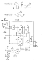
- FIG 3 is a schematic diagram of the preferred embodiment of the interrupt interface circuit of the present invention.
- the illustrated embodiment is designed for operation with a clocked system that is clocked by the system clock signal SYS CLK .
- SYS CLK system clock signal
- An internal interrupt signal CARD IN T is in a low state when no interrupt is being requested by the card.
- CARD INT transitions to a high state when the card is requesting an interrupt and is held there by a latch 32, shown in Figure 3.
- the latching function is usually provided by the logic circuitry providing the internal interrupt signal.
- the internal interrupt signal CARD I N T and the external interrupt signal IRQ are combined in an AND gate 34.
- the third input to the AND gate 34 INT ENABLE is an extra feature possible with this invention, which will be described later.
- INT ENABLE is high.
- the AND gate 34 passes a positive signal to the data input of a D-type flip-flop 36 that has its clock input connected to the system clock SYS CLK.
- the flip-flop 36 outputs on its positive output Q 1 a high signal, as illustrated in Figure 4.
- This signal is passed to the data input of another D-type flip-flop 38, also with its clock input connected to the system clock SYS CLK.
- the complemented output Q 2 is connected to the complemented control input of a tri-state buffer 40, such as a 74LS125, with its input grounded.
- the low level from Q 2 thereby opens the tri-state buffer 40 and grounds the external interrupt line 30 to produce the signal IRQ shown in Figure 4.
- a feedback circuit is provided between the external interrupt line 30 to the AND gate 34 of this circuit as well as to all other similar interrupt interface circuits of this interrupt level.
- the low signal IRQ on the external interrupt line 30 disables the AND gate 34 and, one clock period later, as shown in Figure 4, the Q 1 output of the flip-flop 36 goes low.
- the complemented output Q 2 of the flip-flop 38 goes high and, as a result, the tri-state buffer 40 is disabled and presents a high impedence to the external interrupt line 30. Assuming that no other interrupt circuit is grounding the external interrupt line 30, this line is left floating. However, a pull-up resistor 42 is connected between the external interrupt line 30 and a logic high voltage source, +5V for TTL logic. As a result, the pull-up resistor 42 pulls the signal IRQ on the external interrupt line 30 to a positive high as illustrated in Figure 4 (assuming that the external interrupt line 30 is not grounded by another interrupt interface circuit).
- the pull-up resistor 42 preferably has a resistance value of 8.2 kohmsL which allows a reasonably rapid pull-up of the external interrupt line 30 yet still allows multiple pull-up resistors on the external interrupt line 30 associated with the other interrupt circuits.
- the positive transition 18 of the IRQ signal is the positive transition which is recognized by the INTEL 8259 as indicating a new interrupt request.
- the signal IRQ on the external interrupt line 30 is also fed back to the clock input of yet another D-type flip-flop 44 that has its data input connected to a logic high voltage source, once again +5V.
- the positive transition 18 that is recognized by the INTEL 8259 causes the complemented output Q 3 of flip- flop 44 to go low.
- This signal Q 3 is connected to the complemented clear inputs of the flip-flops 36 and 38.
- the continued low value of the Q 3 signal disables the flip-flops 36 and 38 from producing any further pulses on the external interrupt line 30 regardless of possible new internal interrupt signals CARD INT. It is to be noted that this disabling occurs in the interrupt circuit of Figure 3 even if this particular circuit was not the interrupt circuit producing the interrupt request IRQ on the external interrupt line 30.
- the latch 32 continues to hold the internal interrupt signal CARD INT pending further action.
- the low pulse of the IRQ signal on the external interrupt line 30 disables the AND gate 34 so that any new internal interrupt request CARD INT appearing during the negative IRQ pulse is prevented from propagating to the pulse generator embodied in the flip- flop 38.
- the external interrupt line 30 is connected to one of the interrupt request inputs of the INTEL 8259 controller. All interrupt circuits so connected to a particular INTEL 8259 interrupt input comprise a single interrupt level.
- the INTEL 8259 recognizes the positive transition 18 of the IRQ signal and makes the proper measurement of the high IRQ signal so as to determine which of the interrupt levels is requesting service. Because only a single IRQ pulse is allowed on the external interrupt line 30, there is no possibility of a phantom interrupt. Furthermore, the circuit of Figure 3 does not process second and further pulses for that interrupt level. When an interrupt request is received by the INTEL 8259, it is possible that the request is not immediately serviced because there are higher priority requests outstanding.
- interrupt handler For example, a series of interrupt handlers, illustrated in Figure 5 are provided. There must be at least one interrupt handler for each interrupt interface circuit. Each interrupt handler queries its particular interrupt source to determine if it has an outstanding interrupt request. If the interrupt source does have an outstanding interrupt request, the interrupt handler performs some preassigned task. It should be noted that while only a single interrupt source produced the interrupt request IRQ, there may be several outstanding interrupt requests for the interrupt level. Once the interrupt handler has serviced an outstanding interrupt request, the interrupt handler turns off the internal interrupt signal CARD INT. At this point, two sequences of action are possible.
- the next interrupt handler in the chain of Figure 5 can query its associated interrupt source for the existence of an outstanding interrupt request.
- the processor can terminate its handling of an interrupt signal from the INTEL 8259 after a single handling of an interrupt request.
- the choice between the two sequences depends upon the likelihood of two interrupt requests of the same interrupt level being outstanding concurrently, as balanced against the additional overhead of the polling of the additional levels of interrupt handlers.
- the final step of servicing the interrupt request for a particular level is to reenable the interrupt interface circuits for that level.
- This can be performed by an I/O write to device address 02FX H where X corresponds to the interrupt level. For instance, a command OUT(02F7 H ) causes a reenable signal to all the interrupt interface circuits of interrupt level 7.
- the interrupt interface circuit of Figure 3 has a port to the I/O channel containing the address bus for the addressed I/O device.
- the address bus is connected to an address comparator 46 which compares the address A 0 -A 9 against an internal value, for example, 02F7 H for interrupt level 7. If all the comparisons are true, a high signal is sent to an AND gate 48.
- the address comparator 46 can be replaced by inverters attached to selected address lines A O -A 9 for those address lines which would be zero or low for the present device. Then the address lines A O -A 9 , possibly passing through inverters, are all led to inputs of the AND gate 48. There are two additional inputs to the AND gate 48, an IOW signal indicating an I/O write operation and an AEN signal indicating that the write operation is the type used for the required I/O write rather than a direct memory access write.
- the output of the AND gate 48 is connected through an OR gate 50 to the complemented clear input of the flip-flop 44.
- the function of the other input LOCAL RENABLE to the OR gate will be described later and is an improvement to the invention.
- the OR gate 50 has a complemented output so that, when the OUT(02FX H ) operation addresses the interrupt level of the interrupt interface circuit, the flip-flop 44 is cleared. Barring any further pulses on the external interrupt line 30, the Q 3 output goes high to remove the clear of the flip-flops of 36 and 38, thus reenabling them. Following the reenablement, any active internal interrupt signals CARD INT causes the production of an IRQ pulse on the external interrupt line 30.
- the interrupt enable input INT ENABLE to the AND gate 34 provides the means for disabling the interrupt of a particular interrupt interface circuit. Whenever the INT ENABLE signal is low, the output of the AND gate 34 is always low, thereby preventing the interrupt interface circuit from pulsing an interrupt request on the external interrupt line 30.
- This additional input makes the interrupt interface circuit compatible with software previously written for the IBM PC microcomputer in which there was no interrupt level sharing and the interrupt sources were selectively disabled from producing interrupt requests. This control is necessary in a compatible system where the interrupt mask register of the previously written software would disable all the shared interrupts. Of course, for full sharing of the interrupt level, the INT ENABLE signal is kept high.
- the LOCAL REENABLE input to the OR gate 50 allows a single interrupt interface circuit to monopolize the shared interrupt facility. If an I/O device requires exclusive use of the shared interrupt level, it may effect this control by having its associated interrupt interface circuit disable all other devices. It is of course preferable that this exclusive use of the interrupt level be effected without knowing the details of the other I/O devices sharing the interrupt level.
- an I/O device causes an interrupt, perhaps under the control of the device handler in the system software.
- the interrupt handler in servicing the interrupt request, does not reenable all the interrupt interface circuits of the interrupt level with the previously described OUT(02FX - ), but rather causes a high LOCAL REENABLE.
- the LOCAL REENEABLE is specific to a particular interface circuit and is generally not commonly conveyed to other interrupt interface circuits of the same interrupt level.
- the means of communication between the processor and the interrupt interface circuit for the LOCAL REENABLE signal can be an I/O port using components similar to the address comparator 46 and the AND gate 48. The interrupt handler would then issue an I/O write to a specific address to initiate the LOCAL REENABLE signal.
- the interrupt handler may also choose to revector the interrupt in the INTEL 8259 so that all interrupt requests detected by the INTEL 8259 are directed to the monopolizing interrupt interface circuit.
- the interrupt handler does not issue the OUT(02FX - ) write command, the monopolizing interrupt interface circuit will have exclusive use of the interrupts because the other interrupt circuits remain inhibited by the first negative IRQ pulse on the external interrupt line 30 and have not been subsequently reenabled.
- the device handler In order to reenable the other I/O devices, the device handler must reestablish the original interrupt vector and do the global reenable with an OUT(02FX H ) write instruction.
- the external interrupt line 30 is acting as a bidirectional line.
- the interrupt interface circuits both transmit IRQ pulses on the external interrupt line and also receive these pulses for feedback to the AND gate 34 and the flip- flop 44.
- the IRQ lines 30 cannot be redriven between the interrupt interface circuits comprising a shared interrupt level. All cards using the interrupt sharing mechanism must be in the same unit in the case where drivers are used between units. However, cards for different interrupt levels may occupy different boxes.
- the external interrupt line 30 is one of six lines of an interrupt bus. Each line of the interrupt bus is equivalent and defines the interrupt level.
- the interrupt interface circuit of Figure 3 is for a clocked system.
- An equivalent interrupt interface circuit for an unclocked system is illustrated in the schematic diagram of Figure 6.
- the flip-flops 36 and 38 of Figure 3 are replaced by a one-shot 56 that has a complemented enable input connected to the complemented output Q 3 of the flip-flop 44.
- the remaining elements are similar to those of Figure 3.
- a positive output of the AND gate 34 causes the one- shot 56 to produce a negative pulse on the external interrupt line 30 as long as the one-shot 56 is not disabled by the flip-flop 44.
- a negative pulse on the external interrupt line 30 disables the one-shot 56 until the flip-flop 44 is reenabled.
- the operation of the interrupt interface circuit of Figure 6 is seen to be the same as that of Figure 3 except for the clocking.
- the I/O port for the reenable signal is not explicitly shown nor the added features of Figure 3, which all can be copied from the clocked system.
- the interrupt interface system of the present invention allows the sharing of an interrupt level by multiple interrupt sources.
- the interrupt level sharing can be accomplished at the card level, that is, at the interrupt source.
- the interrupt sharing is accomplished without hardware change to the external interrupt bus or to the INTEL 8259 programmable interrupt controller.
- the software of the interrupt handlers does require modification to provide the polling determination of which interrupt source has an outstanding request for service.
Abstract
Description
- The invention relates generally to computer systems. In particular, the invention relates to the sharing of an interrupt level by multiple interrupt sources.
- A popular type of computer architecture allows multiple users to asynchronously request the service of a resource that is to be used exclusively by the source. One example of the resource is the processor and I/O channel of the computer system. Several I/O devices are attached to the I/O channel and have sufficient intelligence to execute tasks independently of the processor. However, at random times the I/O devices require communication with the processor. In this case, a request is sent to the processor requesting service by the processor. When the processor interrupts its own processing and honors the request, the details of the service request and possibly a response are conveyed on the I/O channel. It is, however, to be understood that the architecture associated with service requests and interrupt is more general than the situation just described.
- One method of servicing these asynchronous requests for service is to have the processor periodically poll all the devices attached to the I/O channel to determine if the device requires service. This method though has several drawbacks. There is a high overhead associated with the polling because the poll must be periodically performed even if there are no outstanding requests. Furthermore, in order to reduce the overhead to a reasonable level, the repetition rate for the polling is made relatively long. As a result,though, the response to a service request becomes slow. In the usual situation, the I/O device making the service request cannot continue its own processing until the service request is serviced by the processor. As a result, system utilization falls with increased time between polls.
- An alternative approach to polling is the use of interrupts or interrupt requests. A dedicated interrupt line is connected between the I/O device and the processor. Whenever the I/O device requires service, that I/O device outputs an interrupt signal onto the interrupt line. A separate interrupt terminal is provided on the processor and the processor, upon detecting an active interrupt line, goes into an interrupt servicing mode to service the request indicated by the interrupt signal. It should be emphasized that the interrupt signal is asynchronous with the operation of the processor and, indeed, is not necessarily synchronized with the processor clock if separate clocks are provided for the processor and the I/O device.
- The computer architecture described above is satisfactory if there is only a single I/O device that is making interrupt request. However, it is more typical that there are several such I/O devices, each asynchronously requesting service by an interrupt signal. Indeed, the trend in modern computer architecture is for increasing intelligence contained in a large number of I/O devices. The communication to the processor, however, is performed over the I/O channel and requires the exclusive utilization of the processor and the I/O channel for the communication between the I/O device and the processor.
- One conventional method of providing for multiple interrupt sources is to use a programmable interrupt controller. A popular programmable interrupt controller is the 8259 manufactured by the Intel Corporation and described in its publication "The 8086 Family Users Manual" dated October 1979 and available from the Intel Corporation in Santa Clara, California. The INTEL controller 8259 allows for eight interrupt levels. Each interrupt level has its own interrupt request line and the eight levels are prioritized among themselves. Whenever an interrupt request line indicates a request for service and the request does not conflict with a higher priority request, the INTEL 8259 outputs an interrupt signal on a single line to the processor that it supports. Along with the interrupt signal to the processor, the INTEL 8259 sends to the processor an interrupt vector associated with that interrupt level. The processor uses the interrupt vector to properly service the interrupt request.
- For multiple interrupt sources, there is always the possibility that two interrupts for a service request are outstanding at a particular time. The INTEL 8259 prioritizes the outstanding requests and, possibly, the request currently being serviced. The highest priority request is serviced first, via the interrupt signal and interrupt vector to the processor, while the outstanding requests are held by the INTEL 8259. Thus, it is seen that the eight interrupt request lines to the 8259 function as separate interrupt levels. Apart from the prioritizing in the case of conflict, the eight different input levels are separable and each is operated similarly to the single interrupt level described above.
- An important aspect of the use of the INTEL 8259 is the convention that an interrupt request signal to the 8259 transitions from a low to a high level to determine that an interrupt request has been received by the INTEL 8259. The convention further states that the interrupt request signal remains high until the request indicated by the interrupt has been serviced. It is a finite time TID after the above described transition that the interrupt request line having the upward transition is measured to determine that it is still high. This measurement indicates which of the interrupt levels are currently asserted. It is to be noted that this high level measurement is redundant.
- A single INTEL 8259 is thus designed to interface the interrupt request line for up to eight I/O devices. However, for modern computer systems this number turns out to be inadequate. For example, the Personal Computer (PC) of the IBM Corporation uses an INTEL 8259 as an interface for the interrupt request lines from the various additional boards plugged into the system or planar board housing the processor. Two of the eight interrupt request lines are, however, used for interrupts originating from the system board. The remaining six interrupt levels are lead to a bus connected to all the slots for additional I/O devices. Thus, there are an insufficient number of interrupt levels for a PC whose I/O slots are completely filled. In fact, some boards require more than one interrupt level. The problem is even worse because a particular board needs to be identified with a particular interrupt level. There are a large number of I/O boards, well in excess of six varieties, and the selection of the particular boards for a PC depends upon the user's needs. If the I/O boards are hard-wired for a particular interrupt level, the possibility arises that the selection of I/O boards is such that a large number of them are using the same interrupt level.
- It would be possible, of course, to expand the number of interrupt levels, even with the continued use of the INTEL 8259. For instance, two or more INTEL 8259s can be used, as described in the previously cited Intel publication and also by Khera in U.S. Patent 4,275, 458. The difficulty with this approach is that it requires the number of interrupt lines that is equal to the number of interrupt levels. It is desirable to provide for additional interrupt sources without modifying the bus connecting the I/O slots to the system board, that is, to continue with the use of only six interrupt levels.
- It is possible to share an interrupt level, that is, that more than one interrupt source is somehow using the same interrupt level. In one version of the PC, the computer system can turn off the interrupt function on one or more boards. Thereby, two or more boards may be sharing an interrupt level but only qpe of them has an operable interrupt at any one time. This approach has the obvious disadvantage that some boards cannot always use their interrupt functions. Furthermore, its use depends upon the predictability of interrupts from particular boards. Such predictability is not assured and runs counter to the architecture of an interrupt driven system.
- Another approach for interrupt level sharing is to provide the possibility of multiple boards outputting active interrupt level signals to a single interrupt request line and then to further provide software routines to determine which of the boards connected to that interrupt level is actually making the request. It is well known that TTL open-collector outputs can be used to share a single electrical line. Unfortunately, open collector outputs can assert a line only if the high level is non-asserted or inactive and the low level is asserted or active. Then, any low open-collector output will pull its connected line low regardless of the high output of any other open-collector output connected to that line. Such a convention is, unfortunately, inconsistent with the requirements of the INTEL 8259 which requires that the low state is inactive and the high state is active. A solution has been proposed by others to accommodate line sharing on the interrupt request inputs to the INTEL 8259. This circuit is illustrated in Figure 1 in which the signal input to a
tri-state buffer 10 is grounded. An enable input to thetri-state buffer 10 is connected to an internal interruptsignal 12. The output of thetri-state buffer 10 is connected to an external interruptline 16 that has a pull-upresistor 14 to a voltage source equal to a high level for the logic circuit, for example, +5V for TTL logic. When the tri-state buffer is not enabled, the pull-upresistor 14 pulls the output up to a high level, assuming that no other buffer connected to the external interruptline 16 is pulling thatline 16 low. However, when thetri-state buffer 10 is enabled by the internal interrupt signal, theoutput line 16 is grounded or put into the low state. The result can also be accomplished with an open-collector output of a TTL circuit. Although it may appear that the negative pulse on theoutput line 16 has the wrong polarity for the INTEL 8259, in fact the INTEL 8259 responds to thepositive transition 18 of the output signal and the output signal remains high following the positive transition to allow the identification of the interrupt level. Once the INTEL 8259 has detected thepositive transition 18, it waits a time T before measuring the high level on the external interruptline 16 to identify the interrupt level making the service request to the INTEL 8259. When that interrupt level is finally serviced, polling is performed by the system to determine which of the interrupt sources of that interrupt level has caused the interrupt. - There are several disadvantages to this approach. One of the most serious disadvantages is the possibility of a phantom interrupt. A phantom interrupt occurs when two interrupt sources of a particular level make closely timed interrupt requests as illustrated in Figure 2. If the first interrupt source produces a
negative pulse 20 on the external interruptline 16 and then, in a time less than TID following theupward transition 18, a second interrupt source produces a secondnegative pulse 22, when the INTEL 8259 measures the input levels on its interrupt request inputs, it detects a low or inactive level on the interruptline 16 of this interrupt level. This situation of a measured low level following an upward transition on an interrupt request input does not conform to the convention for interrupts to an INTEL 8259. The INTEL 8259 is designed so that in such a situation, interrupt level 7 is indicated by default as the level requesting service even though this may not be the case. - The open-collector output approach has the further disadvantage that there may be two outstanding interrupt requests on the same external interrupt line. The second and subsequent requests are not explicity handled by the INTEL 8259. Once the
positive transition 18 has been detected by the INTEL 8259, subsequent positive transitions have no effect until the INTEL 8259 recognizes the interrupt request on the interrupt line and forwards it to the processor. As a'result, when the processor is responding to an interrupt request from a particular interrupt level, it is possible that more than one interrupt source of that interrupt level have an outstanding interrupt request. Thus the processor, once it has received an interrupt from the INTEL 8259, must poll every interrupt source of that level to determine which of them have outstanding requests. Furthermore, it is possible that the processor may be servicing one interrupt request on a particular interrupt level while a second interrupt source requests service. Thus, the only way that it is possible to determine that all outstanding interrupt requests on a particular interrupt level has been serviced is to not only poll each interrupt source of that level but to also to completely poll the sources of that level without finding an outstanding interrupt request. Needless to say, this approach exacts a high overhead for the processor. - Accordingly, it is an object of this invention to provide interrupt level sharing.
- It is a further object of this invention to provide interrupt level sharing with a minimum of processor overhead.
- It is yet another object of this invention to provide interrupt level sharing in which there are no phantom interrupts and in which interrupt requests are not lost.
- A further object of this invention is to provide a method of interrupt level sharing that is transparent to the user and to the hardware of the user.
- The invention can be summarized as an interrupt interface circuit for interrupt level sharing in which a pulse generator outputs an open-collector negative pulse to an external interrupt line, perhaps common to other interrupt interface circuits. The pulse generator is triggered by an internal interrupt signal that stays active until the internal interrupt is serviced. The pulse generator is inhibited from generating any further pulses by any pulse appearing on the external interrupt line, whether generated by this or another interrupt interface circuit of the same interrupt level. A port to the interface circuit from the processor servicing the interrupts provides a signal to remove the inhibition once the interrupt on that interrupt level has been serviced, thereby allowing the generation of previously inhibited interrupt pulses.
- This invention also relates to the method of sharing interrupt levels, which is embodied in the interface interrupt circuit.
-
- Figure 1 is a circuit diagram of a prior art interrupt interface circuit.
- Figure 2 is a timing diagram illustrating the cause of phantom interrupts in the prior art.
- Figure 3 is a schematic diagram of a clocked embodiment of the interrupt interface circuit of the present invention.
- Figure 4 is a timing diagram illustrating the operation of Figure 3.
- Figure 5 is an illustration of the sequence of interrupt servicing by interrupt handlers.
- Figure 6 is a schematic diagram of an unclocked embodiment of the present invention.
- Figure 3 is a schematic diagram of the preferred embodiment of the interrupt interface circuit of the present invention. The illustrated embodiment is designed for operation with a clocked system that is clocked by the system clock signal SYS CLK. At this point, assume that the signal IRQ on an external interrupt
line 30 is in its high state, as illustrated in the timing diagram of Figure 4. An internal interrupt signal CARD INT is in a low state when no interrupt is being requested by the card. However, CARD INT transitions to a high state when the card is requesting an interrupt and is held there by alatch 32, shown in Figure 3. The latching function is usually provided by the logic circuitry providing the internal interrupt signal. The internal interrupt signal CARD INT and the external interrupt signal IRQ are combined in an ANDgate 34. The third input to the ANDgate 34 INT ENABLE is an extra feature possible with this invention, which will be described later. For the present, assume that INT ENABLE is high. In the presence of a'high internal interrupt signal CARD INT and with the external interrupt signal IRQ being high, the ANDgate 34 passes a positive signal to the data input of a D-type flip-flop 36 that has its clock input connected to the system clock SYS CLK. As a result, at the first upward transition of the system clock SYS CLK following the upward transition of the internal interrupt signal CARD INT, the flip-flop 36 outputs on its positive output Q1 a high signal, as illustrated in Figure 4. This signal is passed to the data input of another D-type flip-flop 38, also with its clock input connected to the system clock SYS CLK. As a result, one clock period later a negative transition to a low level appears on the complemented output Q̅2 of the flip-flop 38. The complemented output Q2 is connected to the complemented control input of atri-state buffer 40, such as a 74LS125, with its input grounded. The low level from Q2 thereby opens thetri-state buffer 40 and grounds the external interruptline 30 to produce the signal IRQ shown in Figure 4. - A feedback circuit is provided between the external interrupt
line 30 to the ANDgate 34 of this circuit as well as to all other similar interrupt interface circuits of this interrupt level. As a result, the low signal IRQ on the external interruptline 30 disables the ANDgate 34 and, one clock period later, as shown in Figure 4, the Q1 output of the flip-flop 36 goes low. - Then one clock cycle later, the complemented output Q2 of the flip-
flop 38 goes high and, as a result, thetri-state buffer 40 is disabled and presents a high impedence to the external interruptline 30. Assuming that no other interrupt circuit is grounding the external interruptline 30, this line is left floating. However, a pull-upresistor 42 is connected between the external interruptline 30 and a logic high voltage source, +5V for TTL logic. As a result, the pull-upresistor 42 pulls the signal IRQ on the external interruptline 30 to a positive high as illustrated in Figure 4 (assuming that the external interruptline 30 is not grounded by another interrupt interface circuit). The pull-upresistor 42 preferably has a resistance value of 8.2 kohmsL which allows a reasonably rapid pull-up of the external interruptline 30 yet still allows multiple pull-up resistors on the external interruptline 30 associated with the other interrupt circuits. Thepositive transition 18 of the IRQ signal is the positive transition which is recognized by the INTEL 8259 as indicating a new interrupt request. - The signal IRQ on the external interrupt
line 30 is also fed back to the clock input of yet another D-type flip-flop 44 that has its data input connected to a logic high voltage source, once again +5V. Thus, thepositive transition 18 that is recognized by the INTEL 8259 causes the complemented output Q3 of flip-flop 44 to go low. This signal Q3 is connected to the complemented clear inputs of the flip-flops flops line 30 regardless of possible new internal interrupt signals CARD INT. It is to be noted that this disabling occurs in the interrupt circuit of Figure 3 even if this particular circuit was not the interrupt circuit producing the interrupt request IRQ on the external interruptline 30. Thus, as soon as any one of the interrupt interface circuits attached to the external interruptline 30, defined as the interrupt level of interest, outputs a negative pulse to the external interruptline 30, no further interrupt requests are produced on the external interruptline 30. However, thelatch 32 continues to hold the internal interrupt signal CARD INT pending further action. It is also to be noted that the low pulse of the IRQ signal on the external interruptline 30 disables the ANDgate 34 so that any new internal interrupt request CARD INT appearing during the negative IRQ pulse is prevented from propagating to the pulse generator embodied in the flip-flop 38. - The external interrupt
line 30 is connected to one of the interrupt request inputs of the INTEL 8259 controller. All interrupt circuits so connected to a particular INTEL 8259 interrupt input comprise a single interrupt level. The INTEL 8259 recognizes thepositive transition 18 of the IRQ signal and makes the proper measurement of the high IRQ signal so as to determine which of the interrupt levels is requesting service. Because only a single IRQ pulse is allowed on the external interruptline 30, there is no possibility of a phantom interrupt. Furthermore, the circuit of Figure 3 does not process second and further pulses for that interrupt level. When an interrupt request is received by the INTEL 8259, it is possible that the request is not immediately serviced because there are higher priority requests outstanding. However, eventually the interrupt request of the particular interrupt level is serviced. Software must be provided which handles the interrupt for each interrupt source. For example, a series of interrupt handlers, illustrated in Figure 5 are provided. There must be at least one interrupt handler for each interrupt interface circuit. Each interrupt handler queries its particular interrupt source to determine if it has an outstanding interrupt request. If the interrupt source does have an outstanding interrupt request, the interrupt handler performs some preassigned task. It should be noted that while only a single interrupt source produced the interrupt request IRQ, there may be several outstanding interrupt requests for the interrupt level. Once the interrupt handler has serviced an outstanding interrupt request, the interrupt handler turns off the internal interrupt signal CARD INT. At this point, two sequences of action are possible. The next interrupt handler in the chain of Figure 5 can query its associated interrupt source for the existence of an outstanding interrupt request. Alternatively, the processor can terminate its handling of an interrupt signal from the INTEL 8259 after a single handling of an interrupt request. The choice between the two sequences depends upon the likelihood of two interrupt requests of the same interrupt level being outstanding concurrently, as balanced against the additional overhead of the polling of the additional levels of interrupt handlers. - The final step of servicing the interrupt request for a particular level is to reenable the interrupt interface circuits for that level. This can be performed by an I/O write to device address 02FXH where X corresponds to the interrupt level. For instance, a command OUT(02F7H) causes a reenable signal to all the interrupt interface circuits of interrupt level 7.
- The interrupt interface circuit of Figure 3 has a port to the I/O channel containing the address bus for the addressed I/O device. The address bus is connected to an
address comparator 46 which compares the address A0-A9 against an internal value, for example, 02F7H for interrupt level 7. If all the comparisons are true, a high signal is sent to an ANDgate 48. Theaddress comparator 46 can be replaced by inverters attached to selected address lines AO-A9 for those address lines which would be zero or low for the present device. Then the address lines AO-A9, possibly passing through inverters, are all led to inputs of the ANDgate 48. There are two additional inputs to the ANDgate 48, an IOW signal indicating an I/O write operation and an AEN signal indicating that the write operation is the type used for the required I/O write rather than a direct memory access write. - The output of the AND
gate 48 is connected through anOR gate 50 to the complemented clear input of the flip-flop 44. The function of the other input LOCAL RENABLE to the OR gate will be described later and is an improvement to the invention. TheOR gate 50 has a complemented output so that, when the OUT(02FXH) operation addresses the interrupt level of the interrupt interface circuit, the flip-flop 44 is cleared. Barring any further pulses on the external interruptline 30, the Q3 output goes high to remove the clear of the flip-flops of 36 and 38, thus reenabling them. Following the reenablement, any active internal interrupt signals CARD INT causes the production of an IRQ pulse on the external interruptline 30. - The two extra features in the interrupt interface circuit of Figure 3 will now be described. The interrupt enable input INT ENABLE to the AND
gate 34 provides the means for disabling the interrupt of a particular interrupt interface circuit. Whenever the INT ENABLE signal is low, the output of the ANDgate 34 is always low, thereby preventing the interrupt interface circuit from pulsing an interrupt request on the external interruptline 30. This additional input makes the interrupt interface circuit compatible with software previously written for the IBM PC microcomputer in which there was no interrupt level sharing and the interrupt sources were selectively disabled from producing interrupt requests. This control is necessary in a compatible system where the interrupt mask register of the previously written software would disable all the shared interrupts. Of course, for full sharing of the interrupt level, the INT ENABLE signal is kept high. - The LOCAL REENABLE input to the
OR gate 50 allows a single interrupt interface circuit to monopolize the shared interrupt facility. If an I/O device requires exclusive use of the shared interrupt level, it may effect this control by having its associated interrupt interface circuit disable all other devices. It is of course preferable that this exclusive use of the interrupt level be effected without knowing the details of the other I/O devices sharing the interrupt level. - To gain exclusive use of the shared interrupt, an I/O device causes an interrupt, perhaps under the control of the device handler in the system software. The interrupt handler, in servicing the interrupt request, does not reenable all the interrupt interface circuits of the interrupt level with the previously described OUT(02FX-), but rather causes a high LOCAL REENABLE. The LOCAL REENEABLE is specific to a particular interface circuit and is generally not commonly conveyed to other interrupt interface circuits of the same interrupt level. The means of communication between the processor and the interrupt interface circuit for the LOCAL REENABLE signal can be an I/O port using components similar to the
address comparator 46 and the ANDgate 48. The interrupt handler would then issue an I/O write to a specific address to initiate the LOCAL REENABLE signal. The interrupt handler may also choose to revector the interrupt in the INTEL 8259 so that all interrupt requests detected by the INTEL 8259 are directed to the monopolizing interrupt interface circuit. As long as the interrupt handler does not issue the OUT(02FX-) write command, the monopolizing interrupt interface circuit will have exclusive use of the interrupts because the other interrupt circuits remain inhibited by the first negative IRQ pulse on the external interruptline 30 and have not been subsequently reenabled. In order to reenable the other I/O devices, the device handler must reestablish the original interrupt vector and do the global reenable with an OUT(02FXH) write instruction. - It should be pointed that the external interrupt
line 30 is acting as a bidirectional line. The interrupt interface circuits both transmit IRQ pulses on the external interrupt line and also receive these pulses for feedback to the ANDgate 34 and the flip-flop 44. As a result, the IRQ lines 30 cannot be redriven between the interrupt interface circuits comprising a shared interrupt level. All cards using the interrupt sharing mechanism must be in the same unit in the case where drivers are used between units. However, cards for different interrupt levels may occupy different boxes. - In the IBM PC microcomputer, the external interrupt
line 30 is one of six lines of an interrupt bus. Each line of the interrupt bus is equivalent and defines the interrupt level. - The interrupt interface circuit of Figure 3 is for a clocked system. An equivalent interrupt interface circuit for an unclocked system is illustrated in the schematic diagram of Figure 6. The flip-
flops shot 56 that has a complemented enable input connected to the complemented output Q3 of the flip-flop 44. The remaining elements are similar to those of Figure 3. A positive output of the ANDgate 34 causes the one-shot 56 to produce a negative pulse on the external interruptline 30 as long as the one-shot 56 is not disabled by the flip-flop 44. A negative pulse on the external interruptline 30 disables the one-shot 56 until the flip-flop 44 is reenabled. Thus, the operation of the interrupt interface circuit of Figure 6 is seen to be the same as that of Figure 3 except for the clocking. The I/O port for the reenable signal is not explicitly shown nor the added features of Figure 3, which all can be copied from the clocked system. - Thus it is seen that the interrupt interface system of the present invention allows the sharing of an interrupt level by multiple interrupt sources. The interrupt level sharing can be accomplished at the card level, that is, at the interrupt source. Furthermore, the interrupt sharing is accomplished without hardware change to the external interrupt bus or to the INTEL 8259 programmable interrupt controller. However, the software of the interrupt handlers does require modification to provide the polling determination of which interrupt source has an outstanding request for service.
Claims (8)
Applications Claiming Priority (2)
| Application Number | Priority Date | Filing Date | Title |
|---|---|---|---|
| US629868 | 1984-07-11 | ||
| US06/629,868 US4631670A (en) | 1984-07-11 | 1984-07-11 | Interrupt level sharing |
Publications (3)
| Publication Number | Publication Date |
|---|---|
| EP0167827A2 true EP0167827A2 (en) | 1986-01-15 |
| EP0167827A3 EP0167827A3 (en) | 1986-08-27 |
| EP0167827B1 EP0167827B1 (en) | 1990-12-12 |
Family
ID=24524830
Family Applications (1)
| Application Number | Title | Priority Date | Filing Date |
|---|---|---|---|
| EP85106933A Expired - Lifetime EP0167827B1 (en) | 1984-07-11 | 1985-06-05 | Interrupt level sharing circuit |
Country Status (14)
| Country | Link |
|---|---|
| US (1) | US4631670A (en) |
| EP (1) | EP0167827B1 (en) |
| JP (1) | JPH0690699B2 (en) |
| KR (1) | KR900006919B1 (en) |
| AR (1) | AR242455A1 (en) |
| AU (1) | AU571693B2 (en) |
| BR (1) | BR8503044A (en) |
| CA (1) | CA1226957A (en) |
| DE (1) | DE3580871D1 (en) |
| ES (1) | ES8702676A1 (en) |
| HK (1) | HK12492A (en) |
| MX (1) | MX158689A (en) |
| MY (1) | MY100689A (en) |
| SG (1) | SG110791G (en) |
Cited By (11)
| Publication number | Priority date | Publication date | Assignee | Title |
|---|---|---|---|---|
| EP0199221A1 (en) * | 1985-04-26 | 1986-10-29 | International Business Machines Corporation | Noise resistant interrupt circuits |
| GB2225460A (en) * | 1988-11-25 | 1990-05-30 | Standard Microsyst Smc | Asynchronous interrupt arbitrator |
| EP0393302A1 (en) * | 1989-04-19 | 1990-10-24 | Force Computers Gmbh | Computer with a plurality of installable circuit cards |
| EP0454096A2 (en) * | 1990-04-25 | 1991-10-30 | Mitsubishi Denki Kabushiki Kaisha | Interrupt control circuit and microcomputer system comprising the same |
| EP0469549A2 (en) * | 1990-07-30 | 1992-02-05 | Kabushiki Kaisha Toshiba | Interrupt control unit |
| EP0473806A1 (en) * | 1990-09-03 | 1992-03-11 | International Business Machines Corporation | Apparatus and method for error detection and fault isolation |
| EP0508829A1 (en) * | 1991-04-12 | 1992-10-14 | Mitsubishi Denki Kabushiki Kaisha | IC card |
| EP0557009A1 (en) * | 1992-02-14 | 1993-08-25 | Advanced Micro Devices, Inc. | Apparatus for managing system interrupt operations in a computing system |
| US5448725A (en) * | 1991-07-25 | 1995-09-05 | International Business Machines Corporation | Apparatus and method for error detection and fault isolation |
| DE10047183A1 (en) * | 2000-09-22 | 2002-04-18 | Infineon Technologies Ag | Intermediate digital memory element for transmitting flank signals from an interrupt generator to a CPU without any dead time being caused by the transfer |
| CN1983220B (en) * | 2005-12-17 | 2010-05-05 | 鸿富锦精密工业(深圳)有限公司 | Multiple signal source shared signal inputting circuit |
Families Citing this family (24)
| Publication number | Priority date | Publication date | Assignee | Title |
|---|---|---|---|---|
| US4760516A (en) * | 1986-11-25 | 1988-07-26 | Dialogic Corporation | Peripheral interrupt interface for multiple access to an interrupt level |
| US5261084A (en) * | 1988-05-06 | 1993-11-09 | Nec Corporation | Error judgment method |
| CA1319441C (en) * | 1988-09-09 | 1993-06-22 | Paul R. Culley | Programmable interrupt controller |
| US5101497A (en) * | 1988-09-09 | 1992-03-31 | Compaq Computer Corporation | Programmable interrupt controller |
| JPH02224140A (en) * | 1989-02-27 | 1990-09-06 | Nippon Motoroola Kk | Interruption testing device |
| US5187781A (en) * | 1989-12-19 | 1993-02-16 | International Business Machines Corp. | Shared hardware interrupt circuit for personal computers |
| JPH04318654A (en) * | 1991-02-13 | 1992-11-10 | Hewlett Packard Co <Hp> | Redirection system for interruption to microprocessor |
| US5448743A (en) * | 1992-07-21 | 1995-09-05 | Advanced Micro Devices, Inc. | General I/O port interrupt mechanism |
| US5438677A (en) * | 1992-08-17 | 1995-08-01 | Intel Corporation | Mutual exclusion for computer system |
| US5463752A (en) * | 1992-09-23 | 1995-10-31 | International Business Machines Corporation | Method and system for enhancing the efficiency of communication between multiple direct access storage devices and a storage system controller |
| US5475846A (en) * | 1993-08-11 | 1995-12-12 | Databook Incorporated | Apparatus for processing PCMCIA interrupt requests |
| US5734844A (en) * | 1993-10-08 | 1998-03-31 | Cyrix Corporation | Bidirectional single-line handshake with both devices driving the line in the same state for hand-off |
| US6023743A (en) | 1997-06-10 | 2000-02-08 | International Business Machines Corporation | System and method for arbitrating interrupts on a daisy chained architected bus |
| US6279067B1 (en) * | 1999-01-13 | 2001-08-21 | Ati International Srl | Method and apparatus for detecting interrupt requests in video graphics and other systems |
| JP3478994B2 (en) * | 1999-05-31 | 2003-12-15 | 株式会社日立製作所 | Sensor device |
| US6795884B2 (en) | 2000-12-29 | 2004-09-21 | Intel Corporation | Read-only memory based circuitry for sharing an interrupt between disk drive interfaces |
| US6738848B2 (en) * | 2000-12-29 | 2004-05-18 | Intel Corporation | Decoder-based circuitry for sharing an interrupt between disk drive interfaces |
| US6742060B2 (en) | 2000-12-29 | 2004-05-25 | Intel Corporation | Look-up table based circuitry for sharing an interrupt between disk drive interfaces |
| US6772258B2 (en) * | 2000-12-29 | 2004-08-03 | Intel Corporation | Method and apparatus for sharing an interrupt between disk drive interfaces |
| US6823413B2 (en) * | 2001-06-08 | 2004-11-23 | Oki Electronic Industry Co., Ltd. | Interrupt signal processing apparatus |
| US20030093570A1 (en) * | 2001-06-25 | 2003-05-15 | Bissett Thomas D. | Fault tolerant processing |
| CN1317654C (en) * | 2004-03-17 | 2007-05-23 | 致伸科技股份有限公司 | Edge triggered interruption sharing method |
| US20050262376A1 (en) * | 2004-05-21 | 2005-11-24 | Mcbain Richard A | Method and apparatus for bussed communications |
| US9489618B2 (en) * | 2014-05-27 | 2016-11-08 | Purdue Research Foudation | Electronic comparison systems |
Citations (1)
| Publication number | Priority date | Publication date | Assignee | Title |
|---|---|---|---|---|
| US4419762A (en) * | 1982-02-08 | 1983-12-06 | Sperry Corporation | Asynchronous status register |
Family Cites Families (9)
| Publication number | Priority date | Publication date | Assignee | Title |
|---|---|---|---|---|
| US3597743A (en) * | 1969-03-26 | 1971-08-03 | Digital Applic Inc | Expander for real-time communication between a computer and external devices |
| US3665415A (en) * | 1970-04-29 | 1972-05-23 | Honeywell Inf Systems | Data processing system with program interrupt priority apparatus utilizing working store for multiplexing interrupt requests |
| FR2273317B1 (en) * | 1974-05-28 | 1976-10-15 | Philips Electrologica | |
| US4041471A (en) * | 1975-04-14 | 1977-08-09 | Scientific Micro Systems, Inc. | Data processing system including a plurality of programmed machines and particularly including a supervisor machine and an object machine |
| US4035780A (en) * | 1976-05-21 | 1977-07-12 | Honeywell Information Systems, Inc. | Priority interrupt logic circuits |
| US4090238A (en) * | 1976-10-04 | 1978-05-16 | Rca Corporation | Priority vectored interrupt using direct memory access |
| JPS5363829A (en) * | 1976-11-18 | 1978-06-07 | Sanyo Electric Co Ltd | Generation control system of interrupt signal and interrupt circuit its execution |
| BE887134A (en) * | 1979-12-14 | 1981-05-14 | Gte Automatic Electric Lab Inc | INTERRUPTION EXPANSION CIRCUIT |
| US4420806A (en) * | 1981-01-15 | 1983-12-13 | Harris Corporation | Interrupt coupling and monitoring system |
-
1984
- 1984-07-11 US US06/629,868 patent/US4631670A/en not_active Expired - Lifetime
-
1985
- 1985-03-08 JP JP60045017A patent/JPH0690699B2/en not_active Expired - Lifetime
- 1985-05-15 CA CA000481598A patent/CA1226957A/en not_active Expired
- 1985-05-16 AU AU42550/85A patent/AU571693B2/en not_active Expired
- 1985-06-03 MX MX205500A patent/MX158689A/en unknown
- 1985-06-05 DE DE8585106933T patent/DE3580871D1/en not_active Expired - Lifetime
- 1985-06-05 EP EP85106933A patent/EP0167827B1/en not_active Expired - Lifetime
- 1985-06-08 KR KR8504018A patent/KR900006919B1/en not_active IP Right Cessation
- 1985-06-25 BR BR8503044A patent/BR8503044A/en not_active IP Right Cessation
- 1985-07-03 AR AR85300888A patent/AR242455A1/en active
- 1985-07-10 ES ES545026A patent/ES8702676A1/en not_active Expired
-
1987
- 1987-09-28 MY MYPI87002003A patent/MY100689A/en unknown
-
1991
- 1991-12-31 SG SG1107/91A patent/SG110791G/en unknown
-
1992
- 1992-02-13 HK HK124/92A patent/HK12492A/en not_active IP Right Cessation
Patent Citations (1)
| Publication number | Priority date | Publication date | Assignee | Title |
|---|---|---|---|---|
| US4419762A (en) * | 1982-02-08 | 1983-12-06 | Sperry Corporation | Asynchronous status register |
Non-Patent Citations (2)
| Title |
|---|
| ELEKTRONIK, vol. 32, no. 7, April 1983, page 104, M}nchen, DE; U. KNAPPE: "Interrupt-Steuerung f}r AIM-65" * |
| IBM TECHNICAL DISCLOSURE BULLETIN, vol. 18, no. 3, August 1975, pages 767-768, New York, US; P. FAVRE: "Device for fast I/O selection" * |
Cited By (17)
| Publication number | Priority date | Publication date | Assignee | Title |
|---|---|---|---|---|
| EP0199221A1 (en) * | 1985-04-26 | 1986-10-29 | International Business Machines Corporation | Noise resistant interrupt circuits |
| US4764893A (en) * | 1985-04-26 | 1988-08-16 | International Business Machines Corporation | Noise-immune interrupt level sharing |
| GB2225460A (en) * | 1988-11-25 | 1990-05-30 | Standard Microsyst Smc | Asynchronous interrupt arbitrator |
| FR2639729A1 (en) * | 1988-11-25 | 1990-06-01 | Standard Microsyst Smc | ARBITRATION APPARATUS FOR PROCESSING ASYNCHRONOUS INTERRUPTIONS |
| US5293589A (en) * | 1989-04-19 | 1994-03-08 | Force Computers Gmbh | Circuit with predetermined delay for selectively relaying interrupt signals through a daisy-chain of linked modules upon removal of a module from a slot |
| EP0393302A1 (en) * | 1989-04-19 | 1990-10-24 | Force Computers Gmbh | Computer with a plurality of installable circuit cards |
| EP0454096A2 (en) * | 1990-04-25 | 1991-10-30 | Mitsubishi Denki Kabushiki Kaisha | Interrupt control circuit and microcomputer system comprising the same |
| EP0454096A3 (en) * | 1990-04-25 | 1992-05-20 | Mitsubishi Denki Kabushiki Kaisha | Interrupt control circuit and microcomputer system comprising the same |
| EP0469549A2 (en) * | 1990-07-30 | 1992-02-05 | Kabushiki Kaisha Toshiba | Interrupt control unit |
| EP0469549A3 (en) * | 1990-07-30 | 1992-08-05 | Kabushiki Kaisha Toshiba | Interrupt control unit |
| EP0473806A1 (en) * | 1990-09-03 | 1992-03-11 | International Business Machines Corporation | Apparatus and method for error detection and fault isolation |
| EP0508829A1 (en) * | 1991-04-12 | 1992-10-14 | Mitsubishi Denki Kabushiki Kaisha | IC card |
| US5343030A (en) * | 1991-04-12 | 1994-08-30 | Mitsubishi Denki Kabushiki Kaisha | IC card having flash erase means |
| US5448725A (en) * | 1991-07-25 | 1995-09-05 | International Business Machines Corporation | Apparatus and method for error detection and fault isolation |
| EP0557009A1 (en) * | 1992-02-14 | 1993-08-25 | Advanced Micro Devices, Inc. | Apparatus for managing system interrupt operations in a computing system |
| DE10047183A1 (en) * | 2000-09-22 | 2002-04-18 | Infineon Technologies Ag | Intermediate digital memory element for transmitting flank signals from an interrupt generator to a CPU without any dead time being caused by the transfer |
| CN1983220B (en) * | 2005-12-17 | 2010-05-05 | 鸿富锦精密工业(深圳)有限公司 | Multiple signal source shared signal inputting circuit |
Also Published As
| Publication number | Publication date |
|---|---|
| KR900006919B1 (en) | 1990-09-24 |
| EP0167827A3 (en) | 1986-08-27 |
| JPS6128154A (en) | 1986-02-07 |
| ES8702676A1 (en) | 1986-12-16 |
| MY100689A (en) | 1991-01-17 |
| HK12492A (en) | 1992-02-21 |
| AR242455A1 (en) | 1993-03-31 |
| ES545026A0 (en) | 1986-12-16 |
| US4631670A (en) | 1986-12-23 |
| AU571693B2 (en) | 1988-04-21 |
| EP0167827B1 (en) | 1990-12-12 |
| JPH0690699B2 (en) | 1994-11-14 |
| AU4255085A (en) | 1986-01-16 |
| SG110791G (en) | 1992-02-14 |
| CA1226957A (en) | 1987-09-15 |
| DE3580871D1 (en) | 1991-01-24 |
| KR860001382A (en) | 1986-02-26 |
| BR8503044A (en) | 1986-03-11 |
| MX158689A (en) | 1989-02-27 |
Similar Documents
| Publication | Publication Date | Title |
|---|---|---|
| EP0167827B1 (en) | Interrupt level sharing circuit | |
| US4050097A (en) | Synchronization technique for data transfers over an asynchronous common bus network coupling data processing apparatus | |
| EP0037875B1 (en) | Modular data processing system | |
| EP0130593B1 (en) | Shared resource lockout apparatus | |
| US4519028A (en) | CPU with multi-stage mode register for defining CPU operating environment including charging its communications protocol | |
| US4030075A (en) | Data processing system having distributed priority network | |
| US3995258A (en) | Data processing system having a data integrity technique | |
| US4096569A (en) | Data processing system having distributed priority network with logic for deactivating information transfer requests | |
| US4000485A (en) | Data processing system providing locked operation of shared resources | |
| US4381542A (en) | System for interrupt arbitration | |
| EP0288607A1 (en) | Computer system having a multi-channel direct memory access arbitration | |
| US5805929A (en) | Multiple independent I/O functions on a PCMCIA card share a single interrupt request signal using an AND gate for triggering a delayed RESET signal | |
| CA2055962A1 (en) | Bus arbitration system | |
| KR930002787B1 (en) | Universal peripheral controller self-configuring bootloadable ramware | |
| US5551054A (en) | Page mode buffer controller for transferring Nb byte pages between a host and buffer memory without interruption except for refresh | |
| US4604685A (en) | Two stage selection based on time of arrival and predetermined priority in a bus priority resolver | |
| US5241661A (en) | DMA access arbitration device in which CPU can arbitrate on behalf of attachment having no arbiter | |
| KR900001120B1 (en) | Distributed priority network logic for allowing a low priority unit to reside in a high priority position | |
| US6175887B1 (en) | Deterministic arbitration of a serial bus using arbitration addresses | |
| US3999170A (en) | Multiple access interconnect system | |
| CA1120123A (en) | Automatic data steering and data formatting mechanism | |
| US5377334A (en) | Fast asynchronous resource master-slave combination | |
| US5960180A (en) | Host adapter integrated circuit having autoaccess pause | |
| Borrill | Microprocessor bus structures and standards | |
| WO1994008299A1 (en) | Interrupt request signal noise filter and negative pulse extension circuit |
Legal Events
| Date | Code | Title | Description |
|---|---|---|---|
| PUAI | Public reference made under article 153(3) epc to a published international application that has entered the european phase |
Free format text: ORIGINAL CODE: 0009012 |
|
| AK | Designated contracting states |
Designated state(s): BE CH DE FR GB IT LI NL SE |
|
| PUAL | Search report despatched |
Free format text: ORIGINAL CODE: 0009013 |
|
| 17P | Request for examination filed |
Effective date: 19860523 |
|
| AK | Designated contracting states |
Kind code of ref document: A3 Designated state(s): BE CH DE FR GB IT LI NL SE |
|
| 17Q | First examination report despatched |
Effective date: 19880913 |
|
| GRAA | (expected) grant |
Free format text: ORIGINAL CODE: 0009210 |
|
| AK | Designated contracting states |
Kind code of ref document: B1 Designated state(s): BE CH DE FR GB IT LI NL SE |
|
| REF | Corresponds to: |
Ref document number: 3580871 Country of ref document: DE Date of ref document: 19910124 |
|
| ET | Fr: translation filed | ||
| ITF | It: translation for a ep patent filed |
Owner name: IBM - DR. ALFREDO BRAVI |
|
| ITTA | It: last paid annual fee | ||
| PLBE | No opposition filed within time limit |
Free format text: ORIGINAL CODE: 0009261 |
|
| STAA | Information on the status of an ep patent application or granted ep patent |
Free format text: STATUS: NO OPPOSITION FILED WITHIN TIME LIMIT |
|
| 26N | No opposition filed | ||
| EAL | Se: european patent in force in sweden |
Ref document number: 85106933.6 |
|
| REG | Reference to a national code |
Ref country code: GB Ref legal event code: IF02 |
|
| PGFP | Annual fee paid to national office [announced via postgrant information from national office to epo] |
Ref country code: BE Payment date: 20020605 Year of fee payment: 18 |
|
| PGFP | Annual fee paid to national office [announced via postgrant information from national office to epo] |
Ref country code: CH Payment date: 20020919 Year of fee payment: 18 |
|
| PG25 | Lapsed in a contracting state [announced via postgrant information from national office to epo] |
Ref country code: LI Free format text: LAPSE BECAUSE OF NON-PAYMENT OF DUE FEES Effective date: 20030630 Ref country code: CH Free format text: LAPSE BECAUSE OF NON-PAYMENT OF DUE FEES Effective date: 20030630 Ref country code: BE Free format text: LAPSE BECAUSE OF NON-PAYMENT OF DUE FEES Effective date: 20030630 |
|
| BERE | Be: lapsed |
Owner name: *INTERNATIONAL BUSINESS MACHINES CORP. Effective date: 20030630 |
|
| REG | Reference to a national code |
Ref country code: CH Ref legal event code: PL |
|
| PGFP | Annual fee paid to national office [announced via postgrant information from national office to epo] |
Ref country code: SE Payment date: 20040511 Year of fee payment: 20 |
|
| PGFP | Annual fee paid to national office [announced via postgrant information from national office to epo] |
Ref country code: GB Payment date: 20040601 Year of fee payment: 20 |
|
| PGFP | Annual fee paid to national office [announced via postgrant information from national office to epo] |
Ref country code: DE Payment date: 20040615 Year of fee payment: 20 |
|
| PGFP | Annual fee paid to national office [announced via postgrant information from national office to epo] |
Ref country code: FR Payment date: 20040621 Year of fee payment: 20 |
|
| PGFP | Annual fee paid to national office [announced via postgrant information from national office to epo] |
Ref country code: NL Payment date: 20040630 Year of fee payment: 20 |
|
| PG25 | Lapsed in a contracting state [announced via postgrant information from national office to epo] |
Ref country code: GB Free format text: LAPSE BECAUSE OF EXPIRATION OF PROTECTION Effective date: 20050604 |
|
| PG25 | Lapsed in a contracting state [announced via postgrant information from national office to epo] |
Ref country code: NL Free format text: LAPSE BECAUSE OF EXPIRATION OF PROTECTION Effective date: 20050605 |
|
| REG | Reference to a national code |
Ref country code: GB Ref legal event code: PE20 |
|
| NLV7 | Nl: ceased due to reaching the maximum lifetime of a patent |
Effective date: 20050605 |
|
| EUG | Se: european patent has lapsed |