EP0174099A2 - Fiber optic terminal interface - Google Patents
Fiber optic terminal interface Download PDFInfo
- Publication number
- EP0174099A2 EP0174099A2 EP85305545A EP85305545A EP0174099A2 EP 0174099 A2 EP0174099 A2 EP 0174099A2 EP 85305545 A EP85305545 A EP 85305545A EP 85305545 A EP85305545 A EP 85305545A EP 0174099 A2 EP0174099 A2 EP 0174099A2
- Authority
- EP
- European Patent Office
- Prior art keywords
- data
- signal
- video
- generating
- digital
- Prior art date
- Legal status (The legal status is an assumption and is not a legal conclusion. Google has not performed a legal analysis and makes no representation as to the accuracy of the status listed.)
- Granted
Links
Images


Classifications
-
- H—ELECTRICITY
- H04—ELECTRIC COMMUNICATION TECHNIQUE
- H04N—PICTORIAL COMMUNICATION, e.g. TELEVISION
- H04N7/00—Television systems
- H04N7/22—Adaptations for optical transmission
-
- G—PHYSICS
- G06—COMPUTING; CALCULATING OR COUNTING
- G06F—ELECTRIC DIGITAL DATA PROCESSING
- G06F3/00—Input arrangements for transferring data to be processed into a form capable of being handled by the computer; Output arrangements for transferring data from processing unit to output unit, e.g. interface arrangements
- G06F3/14—Digital output to display device ; Cooperation and interconnection of the display device with other functional units
- G06F3/153—Digital output to display device ; Cooperation and interconnection of the display device with other functional units using cathode-ray tubes
Definitions
- the present invention relates to the manner of connecting a user input/output terminal to a data processing syste .
- Such a connection is required in the case in which a single data processing system supports a number of user terminals, or in the case in which a data processing system supports only a single user terminal which is located remotely from the data processing system.
- a communications link between the data processing system and the user terminal is required in order to provide the required interaction between these elements.
- the present invention relates to this communications link.
- the user terminals of the type to which the present invention is applicable include a variety of input and output devices.
- the major output device used in such user terminals is a video display.
- a video display is typically a raster scanned cathode ray tube which provides graphic and pictorial information to the user.
- the terminal may also include a tone generator for generating tones which may serve as audible alarms or the like.
- Such a user terminal may further include some type of synthetic speech synthesis device which provides a machine generated output in a human language which may be understood by a naive user.
- such a device may include one or more indicator lights which are controlled by the data processing syste .
- User terminals of the type to which the present invention is applicable typically employ a manually actuated typewriter style keyboard as the major input device. This keyboard is employed by manually depressing one or more keys to compose textural messages for transmission to the data processing syste .
- Another type of widely used input device is a mouse.
- a mouse is a pointing device employed with a video display screen. A cursor or indicating device on the screen is moved in correspondence to the movement of the mouse on a surface such as a desk adjacent to the user terminal.
- a mouse of this type may also include one or more user actuatable switches which serve to transmit condition signals from the user to the data processing apparatus.
- an interface of the type to which the present invention pertains includes bidirectional communication of varying bit rates.
- the communications link of this type There are mechanical and electrical requirements for the communications link of this type. Firstly, the weight and bulk of the communications link between these two systems needs to be minimized. A minimal weight and bulk will permit easier installation of this communications link. In addition, it is also desirable that the cable employed for this purpose be flexible in order to be able to better conform to the routing requirements of any specific installation. Typically, such communications links would be installed in office locations such as used by an engineer or other technical worker. Other electronic devices are commonly employed in such an environment.
- Electromagnetic interference (EMI) and radio frequency interference (RFI) are types of radiated energy which might eminate from such a communications link. Particularly in the case in which a high bit rate is required, therefore requiring high frequency signals on the communications link, it is necessary to make special provisions to minimize the amount of energy radiated. Minimization of this radiated energy serves to minimize the interference of this particular communications link with other electrical systems employed in this same area.
- MOS metal oxide semiconductor
- a further problem with such communications links is ground shift. Electrically shielded high frequency copper wires typically use wire shields tied to chassis ground. When two chassis are located remotely, it is possible that they are tied to differing branches of the electric power lines and thus have differing chassis ground potentials. This causes unwanted current through the wire shield which can cause numerous problems.
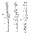
- FIG. 1 illustrates the general construction of an apparatus such as employed in the preferred embodiment of the present invention.
- This apparatus includes a central processing unit 110, a graphics controller 120 and a user terminal 130.
- the central processing unit 110 is in bidirectional communication with graphics controller 120 via communication links 112 and 116.
- graphics controller 120 is in bidirectional communication with user terminal 120 via communication links 122 and 126.
- a dashed line 140 encloses both central processing unit 110 and graphics controller 120. This dashed line 140 indicates the parts which are included within a single enclosure. In the event that computing system 100 serves a single user, it would be desirable to place all of these units within a single enclosure.
- central processing unit and the graphics controller are in one enclosure and the user terminal is in the other as illustrated in Figure 1.
- the central processing unit is in a single unit and the graphics controller and the user terminal share one enclosure.
- the communication between central processing unit 1 10 and graphics controller 120 is necessarily of a high data rate. Therefore it is considered advantageous to enclose both central processing unit 110 and graphics controller 120 in the same enclosure.
- central processing unit 140 and graphics controller 120 are placced within the same enclosure 140. Therefore, communication links 122 and 126 must pass from enclosure 140 to user-terminal 130. In this event, both communication links 122 and 126 encounter the mechanical and electrical problems noted above.
- FIG. 2 illustrates the configuration of the transmitters and receivers on communication links 122 and 126 in accordance with the preferred embodiment of the present invention.
- Transmitter 210 and receiver 220 are located within graphics controller 120.
- Receiver 230 and transmitter 240 are located within user terminal 130.
- Transmitter 210 transmits data on communication link 122 to receiver 230.
- Transmitter 210 receives video input 211, keyboard input 212 (which may control keyboard indicators or control the keyboard configuration) and sound input 213.
- Receiver 230 receives this data on communication link 112.
- Receiver 230 then separates out video data 231, keyboard data 232 and sound data 233 for application to those portions within user terminal 130 which employ this data (not illustrated). These features are conventional in nature.
- Receiver 230 also outputs clock signal 235 which is derived from signals received on communication link 122.
- both communications links 122 and 126 are formed of optical fibers.
- the use of optical fibers for the communications links minimizes the mechanical and electrical problems with such communications links.
- fiber optic cables are very small and consequently such cables have relatively small weight and bulk. These cables are also flexible in comparison to the prior art copper coaxial cables. Thus fiber optic cables contribute to the solution to the mechanical problems associated with such communications links.
- fiber optic cables contribute to the solution to the electrical problems with such communications link .
- This lack of oscillatory electrical currents which is in contrast to the prior art copper coaxial cables, is the factor which makes fiber optic cables advantageous.
- the major causes of electromagnetic interference (EMI) and radio frequency interference (RFI) are those oscillatory electrical currents.
- EMI electromagnetic interference
- RFID radio frequency interference
- fiber optic cables substantially reduce this source of electrical problems.
- fiber optic cables are nonconducting. For this reason there is also a substantially reduced chance of damaging electrostatic discharge (ESD) from fiber optic cables as opposed to the prior art copper coaxial cables. Note that such a fiber optic link prevents an electrostatic discharge path between the user terminal, where static is most likely to be generated, and the central processing unit, where it is most damaging.
- Receiver 220 within graphics controller 120 receives data on communications link 126 from transmitter 240 located in user terminal 130. Transmitter 240 has applied to it keyboard data 241, mouse data 242 and speech data 243. Transmitter 240 also receives clock 235 from receiver 230. Transmitter 240 takes the incoming data together with the clock signal and generates a transmission on communications link 126 in the form required by communications link 126. This is then applied to receiver 220 within graphics controller 120. Receiver 220 converts the signal from communications link 126 into its component signals, namely keyboard data 221, mouse data 222 and speech data 223. This data is then applied to central processing unit 110 for processing by that element.
- Figures 3(A) to 3(C) illustrate the format of the preferred embodiment of the communications from graphics controller 120 to user terminal 130 on communications link 122.
- Figure 3(A) illustrates the form of data transmitted on communications link 122 during normal horizontal scan periods.
- the video signals are transmitted in digital form.
- each pixel of the display can be represented by a single bit.
- This digital video data is transmitted in a set of horizontal scan lines in accordance with the prior technicques concerning analog video signals.
- Figure 3(B) illustrates the form of communications transmitted during vertical retrace intervals.
- Figure 3(C) illustrates the form of the coded data 320 transmitted during the horizontal retrace intervals.
- Signal 310 illustrates the parts of the data transmitted on communications link 122 during normal horizontal trace intervals.
- This signal 310 is composed of uncoded video data 315 and coded data 320.
- the uncoded data 315 is preferably a single bit for each pixel for each horizontal line on the video display.
- a zero in a particular bit position would cause the corresponding pixel on that line within the video display to be black.
- a one in that bit position would cause the corresponding pixel on the video screen to be white.
- Communications link 122 could carry analog signals to enable a gray scale.
- the required bit rate for the communications link is for the most part set by the number of pixels on the video screen and therefore the number of bit positions within uncoded video data 315.
- each uncoded video data portion 315 must have 1,000 bits and it requires transmission of 1,000 uncoded video data portions 315 in order to transmit the entire video screen. Therefore, each video screen includes approximately one million bits.
- JF s ordinarily considered necessary to transmit 60 complete frames per second.
- the data rate for such a high quality video screen is at least 60 million bits per second.
- Coded data 320 of signal 310 contains the keyboard and sound portions together with other auxilliary data. This coded data 320 is further illustrated in Figure 3(C).
- Signal 330 illustrates the signal on communications link 122 during the vertical retrace interval.
- the cathode ray spot is returned to the upper right hand corner.
- this time interval which may equal the time interval of several horizontal scans, the incoming video data is ignored. Therefore, the video data transmitted during this portion of a scan cycle is unimportant.
- a square wave signal 335 is transmitted during this vertical retrace interval.
- coded data 320 is transmitted at the end of each of the horizontal scan lines which make up the vertical retrace interval, in the same manner as in the normal horizontal scan signal 310.
- Coded data 320 is illustrated in detail in Figure 3(C).
- the coded data 320 includes sync pattern 321, vertical sync 322, keyboard data 323, speech data 324, sound data 325 and test data 326.
- Sync pattern 321 is employed to signal to the user terminal the end of a horizontal scan line.
- the horizontal sync signal is communicated via an analog signal outside the range of permissible video signals.
- the video data is transmitted as a digital signal. Therefore, it is necessary to provide another means for identifying the end of a horizontal scan line.
- the sync pattern 321 is a predetermined set of bits. As will be more fully explained below in conjunction with Figure 5, the receiving apparatus in the user terminal detects this predetermined set of bits corresponding to sync pattern 321 as will be further explained below, this also initializes the decoding of coded data 320.
- Vertical sync 322 serves a function similar to sync pattern 321. Vertical sync 322 is employed to indicate when a frame reset is required.
- coded data 320 corresponds to data transmitted from the graphics controller 120 to user terminal 130.
- Keyboard data 323 serves to control any keyboard indicators and to control the configuration of the keyboard.
- Speech data 324 is employed in conjunction with a speech synthesis circuit. Speech data 324 specifies the particular synthetic speech to be produced at user terminal 130.
- sound data 325 is employed in conjunction with an audible sound generator. Sound data 325 is employed within user terminal 130 to indicate the type of sounds to be produced by this sound generator.
- test data 326 is employed by user terminal 130 in order to test various aspects of this unit under the control of the central processing unit 110.
- coded data 320 is not exhaustive. It would be clear to those skilled in the art that other forms of coded data may be transmitted via coded data 320 than those illustrated in Figure 3 and noted above. In particular, it should be noted that ordinarily the data rate required for the data within coded data portion 320 is much less than the data required for uncoded video data 315. Therefore, coded data 320 may be transmitted at a much lower bit rate. This much lower bit rate would require much less sophisticated decoding than would be required if it were transmitted at the rate of the uncoded video data.
- FIG. 4 illustrates transmitter 400 located within the graphics controller.
- Transmitter 400 generates an optic output on communications link 122 which is then applied to the receiver in user terminal 130.
- Transmitter 400 includes parallel to serial shift register 410.
- Parallel to serial shift register 410 has numerous data and control inputs supplied thereto.
- the data inputs include vertical sync 411, keyboard data 412, sound data 413, speech data 414, sync code 415 and the test data 416. Although each of these data inputs is illustrated as including a single line, it should be understood that each of these signals may include a plurality of bits applied to parallel to serial shift register 410.
- Parallel to serial shift register 410 is controlled by load signal 417 and shift signal 418 from timing and control logic 420.
- the output from parallel to serial shift register 410 is serial data 431.
- Timing and control logic 420 performs the major control functions within transmitter 400. Timing and control logic 420 receives a clock input 421 and a horizontal synchronization input 422. Timing and control logic 420 then produces various signals at the time required by the other elements of transmitter 400. Timing and control logic 420 produces load signal 417 and shift signal 418 to parallel to serial shift register 410. Load signal 417 is applied to sh-ift register 410 when shift register 410 is being loaded with the various data bits. Shift signal 418 causes shift register 410 to no longer receive inputs but to shift its contents out as serial data 451 to Manchester encoder 430.
- Manchester encoder 430 receives the serial data 431 from shift register 410 and further receives clock 452 from timing and control logic 420.
- Clock 432 may have a different frequency than clock 421 applied to timing and control logic 420.
- Manchester encoder 430 takes an exclusive OR of serial data 431 and clock signal 432 thereby producing encoded data 431. This encoded data 441 is applied to multiplexer 440.
- Multiplexer 440 serves to combine various signals under the control of timing and control logic 420.
- Multiplexer 440 receives the encoded data 441 from Manchester encoder 430.
- Multiplexer 440 also receives uncoded video 442.
- Multiplexer 440 receives square wave 443 and control 444 from timing and control logic 420.
- Multiplexer 440 operates in accordance with control 444 to apply one of encoded data 441, video data 442 or square wave 443 to electrical output 445.
- video data 443 is coupled to electrical output 445.
- encoded data 441 is applied to electrical output 445.
- multiplexer 440 serves to assemble and combine the signals illustrated in Figure 3. Timing and control logic 440 places the proper signals on control 444 enabling multiplexer 440 to perform this function.
- Fiber optic transmitter 450 converts an electrical signal into an optical signal.
- the communications link 122 between graphic controller 120 and user terminal 130 is via an optic fiber.
- Fiber optic transmitter 450 receives electrical output 445 from multiplexer 440. Fiber optic transmitter 440 then converts this to optical output 451. This optical output 451 is applied to an optic fiber (not shown) which forms communications link 122.
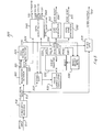
- FIG. 5 illustrates receiver 500.
- Receiver 500 is located in user terminal 130 and receives an input on communication link 122. This appears as optical input 511 to fiber optic receiver 510. As explained in further detail below, receiver 500 generates outputs for use by the utilization portions of the user terminal.
- Fiber optic receiver 510 serves as the input to receiver 500.
- Fiber optic receiver 510 receives an optical input 511 from communications link 112.
- Fiber optic receiver 5-10 then converts this optical input into an electrical input 512 which is applied to both video gate 515 and Manchester decoder 520.
- optical put511 includes portions corresponding to uncoded video date 315 on square wave signal 335 and portions corresponding to coded data 320.
- Video gate 515 and Manchester decoder 520 are employed to separate these respective components.
- Manchester decoder 520 is constructed in order to recover the clock signal from Manchester encoded data. Once this clock signal has been recovered, then it is possible to separate this encoded data from the encoded video data. Manchester decoder 520 then produces clock signal 521 and data signal 522.
- Clock signal 521 and data signal 522 are applied to sync pattern detector 525.
- Sync pattern detector 525 checks to determine whether the sync pattern 321 has been received. When sync pattern 321 has been received, a sync signal 526 is generated. The reception of sync pattern 321 is most important as it marks the end of the uncoded video data 315 or square wave signal 335 and the beginning of coded data 320. This is clearly an important time, and sync signal 526 signals the detected reception of sync pattern 321.
- Event counter 530 works in conjunction with windowed gate 531, phase locked loop oscillator 532 and reset select gate 533 in order to provide proper timing and control signals for the output portions of receiver 500. Then event counter 530 counts pulses received from phase locked loop oscillator 532. Dependent upon this count, event counter then generates signals at its output such as gate signal 534, sync signal 535, valid signal 536, gate signal 537 and reset signal 538.
- Phase lock loop oscillator 532 generates timing pulses used by event counter 530 to control the various events in receiver 500.
- Phase locked loop oscillator 532 is in turn controlled by windowed gate 531.
- Windowed gate 531 receives sync signal 536 from sync pattern detector 525 and a gate signal 534 from event counter 530.
- Windowed gate 531 applies a rate signal to phase locked loop oscillator 532 in order to control its frequency and thereby the timing of event counter 530. This rate signal is dependent upon the rate at which sync signal 526 is received from sync pattern detector 525.
- Gate signal 534 is employed in order to prevent false rate signals caused by false detection of a signal pattern.
- Event counter 530 produces gate signal 534 in order to enable windowed gate 531 only during a predetermined interval near the expected time of arrival of sync pattern 321 and hence sync signal 526.
- gate signal 534 is of a variable duration depending upon the quality of the phase ,iock on the sync pattern 321. That is, window gate 531 would be enabled for longer periods under the control of gate signal 534 when a good phase lock has not been achieved. On the other hand, windowed gate 534 would only be enabled for a short period of time once the quality of the phase lock has improved.
- the timing of events from event counter 530 is in phase with the reception of sync pattern 321 from communication link 122.
- the count within event counter 530 is reset by reset select gate 533.
- Reset select gate 533 resets event counter 530 based upon two contingencies. In the normal case, reset signal 538 from event counter 530 occurs nearly simultaneously with sync signal 526. In this event, reset select gate 533 resets event counter upon reception of reset signal 538. This prevents any slight jitter in reception and detection of sync pattern 321 from interferring with normal operation. If reset signal 538 and sync signal 526 drift apart in time further than a preset limit, and if this condition lasts for several cycles, then reset select gate 533 switches to operation upon reception of sync signal 526. This continues until reset signal 538 and sync signal 526 are again received within the preset limit apart, whereupon normal operation resumes. This prevents false triggering to continue in the event that reset signal 538 drifts away from sync signal 526.
- event counter 530 properly controls the output portion cf receiver 500.
- Event counter 530 produces a gate signal 537 which is applied to video gate 515. This permits video gate 515 to pass the electrial input 512 to video output 513. This gate signal 537 is applied during the period of reception of uncoded video data 315.
- the time at which video gate 515 is opened is timed in conjunction with the internal count of event counter 530 in order to correspond to the interval of reception of uncoded video data 315.
- video output 513 includes successive scan lines of uncoded video data 315 with coded data 320 removed. During vertical retrace intervals, video gate 515 is turned off so that neither square wave signal 335 nor encoded data 320 appears at video output 513.
- Data multiplexer 540 receives data signal 522 from Manchester decoder 520 and a valid data signal 536 from event counter 530.
- the data signal 522 from Manchester decoder 520 is a serial bit stream which is loaded into data de-multiplexer 540 during a loading phase.
- data multiplexer 540 Upon reception of a valid data signal from event counter 530, data multiplexer 540 generates parallel outputs to various portions of user terminal 130. These outputs include keyboard output 541, sound output 542, speech output 543 and test output 544. These multibit data signals are utilized by various portions of user terminal 130 in a conventional manner. When valid data signal 536 is not received from event counter 530, then data demultiplexer 540 does not generate these various output signals.
- Horizontal sync generator 550 and vertical sync generator 555 generate synchronization signals to the video portion of user terminal 130 in order to control the horizontal and vertical scanning motion. Both horizontal sync generator 550 and vertical sync generator 555 receive sync signal 535 from event counter 530. This sync signal 535 is received from event counter 530 other than directly from sync pattern detector 525 in order to reduce the instances of false sync detection. Event counter 530 with windowed gate 531 and phase locked loop oscillator 532 provides a more reliable indication of the reception of sync pattern 321 with fewer false indications than that received directly from sync pattern detector 525. Horizontal sync generator 550 generates horizontal sync signal 551 directly from sync signal 535. On the other hand, vertical sync generator 555 receives an additional input.
- vertical sync signal 545 This additional input is vertical sync signal 545.
- vertical sync signal 322 is a part of coded data 320.
- vertical sync 322 is a portion of coded data 320 and thus data signal 522 applied to data demultiplexer 540. From the occurrence of both sync signal 535 and vertical sync signal 545, vertical sync generator 535 generates vertical reset signal 536. This is employed in the video display.terminal in order to reset the video frame.
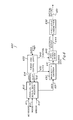
- FIG. 6 illustrates transmitter 600 which is located in user terminal 130.
- Transmitter 600 transmits keybdard, mouse and speech data from user terminal 130 to graphics controller 120 via communications link 126.
- Input data to transmitter 600 is applied to parallal to serial shift register 610.
- each of these data inputs preferably includes a plurality of parallel bits.
- This data is loaded into parallel to serial shift register 610 in accordance with load command 614 from timing and control logic 620..
- parallel to serial shift register 610 Upon reception of shift signal 615, parallel to serial shift register 610 applies serial data 631 to manchester encoder 630.
- Timing and control logic 620 performs the major timing and control functions of transmitter 600. Timing and control logic 620 receives clock signal 621 from receiver 500. This clock signal 621 is related to clock signal 521 produced by Manchester decoder 520. By this means, transmitter 600 is tied to the same Manchester clock signal as transmitter 400 in graphics controller 120.
- Timing and control logic 620 produces load signal 614 and shift signal 615 in the proper time to enable parallel to serial conversion of the input data by parallel to serial shift register 610. Timing and control logic 620 also produces clock signal 632 to be applied to Manchester encoder 630. Manchester encoder 630 operates to combine OR data 631 and clock 632 to produce encoded data 641.
- Timing and control logic further generates control signal 642 which is applied to sync signal adder 640.
- ' Sync signs adder 640 receives encoded data 641 from manchester decoder 630 and add a sync signal similar to sync pattern 321 of coded daats 320 to the encoded data 641. The time at which this sync signal is applied is controlled by control signal 642.
- Sync signal adder 640 thus produces electrical output 645.
- Fiber optic transmitter 650 receives electrical output 645. Fiber optic transmitter 650 produces optical output 65a. corresponding to electrical output 645. This optical output 651 is applied to an optic fiber (not shown) forming communications link 126. Thus, the keyboard, mouse and speech data is applied to communications link 126.
- FIG. 7 illustrates receiver 700 located in graphics controller 120.
- Receiver 700 is connected to communications link 126 and receives the signals transmitted by transmitter 600.
- Receiver 700 includes fiber optic receiver 710 which receives optical input 711. This is from the optic fiber which forms communications link 126. In accordance with the received optical input 711, fiber optic receiver 710 generates electrical input 712.
- Manchester decoder 720 The electrical input 712 is applied to Manchester decoder 720.
- Manchester decoder 720 In a manner similar to that descri-bed above in conjunction with Manchester decoder 520, Manchester decoder 720 generates clock 721 corresponding to the clock 632 employed in Manchester encoder 630 and data 722. This data 722 corresponds to the original data received by transmitter 600.
- Clock 721 and data 722 are applied to serial to parallel shift register 730.
- the parallel outputs from serial to parallel shift register 730 are applied to output latch 740.
- Output latch 740 also receives a latch clock signal 726 from sync detector 725.
- Sync detector 725 receives electrical input 712 and generates the latch clock signals 726 upon detection of the appropriate sync signal.
- This sync signal is the sync signal applied to the encoded data by sync signal adder 640.
- Sync detector 725 indicates this detection via latch clock 726.
- output latch 740 generates keyboard data 741, mouse data 742 and speech data 743 corresponding to the data input to transmitter 600. This data is employed in graphics controller 120 and central processing unit 110. These signals from user terminal 130 are employed then to control the operation of the data processing apparatus.
Abstract
Description
- The present invention relates to the manner of connecting a user input/output terminal to a data processing syste . Such a connection is required in the case in which a single data processing system supports a number of user terminals, or in the case in which a data processing system supports only a single user terminal which is located remotely from the data processing system. A communications link between the data processing system and the user terminal is required in order to provide the required interaction between these elements. The present invention relates to this communications link.
- The user terminals of the type to which the present invention is applicable include a variety of input and output devices. The major output device used in such user terminals is a video display. A video display is typically a raster scanned cathode ray tube which provides graphic and pictorial information to the user. The terminal may also include a tone generator for generating tones which may serve as audible alarms or the like. Such a user terminal may further include some type of synthetic speech synthesis device which provides a machine generated output in a human language which may be understood by a naive user. In addition, should there be a limit on types of ancillary data, such a device may include one or more indicator lights which are controlled by the data processing syste .
- User terminals of the type to which the present invention is applicable typically employ a manually actuated typewriter style keyboard as the major input device. This keyboard is employed by manually depressing one or more keys to compose textural messages for transmission to the data processing syste . Another type of widely used input device is a mouse. A mouse is a pointing device employed with a video display screen. A cursor or indicating device on the screen is moved in correspondence to the movement of the mouse on a surface such as a desk adjacent to the user terminal. A mouse of this type may also include one or more user actuatable switches which serve to transmit condition signals from the user to the data processing apparatus. In addition, it is possible for such a user terminal to include a microphone for receiving spoken messages which may be interpreted in conjunction with a speech recognition system.
- It can be seen that even the simplest type of user terminal requires bidirectional communication. In the event that the data processing system transmits video data to the user terminal, this communication must be at a high bit rate. This is in contrast to data such as from a keyboard which is passing from the user terminal to the data processing system, which is ordinarily of a low bit rate. Thus, an interface of the type to which the present invention pertains includes bidirectional communication of varying bit rates.
- There are mechanical and electrical requirements for the communications link of this type. Firstly, the weight and bulk of the communications link between these two systems needs to be minimized. A minimal weight and bulk will permit easier installation of this communications link. In addition, it is also desirable that the cable employed for this purpose be flexible in order to be able to better conform to the routing requirements of any specific installation. Typically, such communications links would be installed in office locations such as used by an engineer or other technical worker. Other electronic devices are commonly employed in such an environment.
- This brings to mind the electrical requirements for such a communications link. Electromagnetic interference (EMI) and radio frequency interference (RFI) are types of radiated energy which might eminate from such a communications link. Particularly in the case in which a high bit rate is required, therefore requiring high frequency signals on the communications link, it is necessary to make special provisions to minimize the amount of energy radiated. Minimization of this radiated energy serves to minimize the interference of this particular communications link with other electrical systems employed in this same area.
- On a similar line, it is desirable to provide a type of communications link which minimizes electrostatic discharge (ESD). The data processing system and the user terminal would typically be constructed using metal oxide semiconductor (MOS) devices. These MOS devices are highly suceptible to static electricity and are vulnerable to electrostatic discharge. Therefore, it would be highly desirable to provide such a communications link which minimized or eliminated electrostatic discharge.
- A further problem with such communications links is ground shift. Electrically shielded high frequency copper wires typically use wire shields tied to chassis ground. When two chassis are located remotely, it is possible that they are tied to differing branches of the electric power lines and thus have differing chassis ground potentials. This causes unwanted current through the wire shield which can cause numerous problems.
- These and other advantages and features of the invention will be further described below in the detailed description of the invention taken in conjunction with the drawings in which:
- Figure 1 illustrates the general outline of the data processing system and user terminal combination to which the present invention is applicable;
- Figure 2 illustrates the details of the transmitters and receivers and the dual channel communications system according to the preferred embodiment of the present invention;
- Figure 3 illustrates the form of the data transmitted from the data processing system to the user terminal in accordance with the preferred embodiment of the present invention;
- Figure 4 illustrates the preferred embodiment of the transmitter located within the data processing system of the present invention;
- Figure 5 illustrates the preferred embodiment of the receiver within the user terminal;
- Figure 6 illustrates the preferred embodiment of the transmitter within the user terminal; and
- Figure 7 illustrates the preferred embodiment of the receiver within the data processing system.
- The features and particulars of the preferred embodiment of the present invention will now be described in detail. Figure 1 illustrates the general construction of an apparatus such as employed in the preferred embodiment of the present invention. This apparatus includes a central processing unit 110, a
graphics controller 120 and auser terminal 130. The central processing unit 110 is in bidirectional communication withgraphics controller 120 viacommunication links graphics controller 120 is in bidirectional communication withuser terminal 120 viacommunication links graphics controller 120. This dashed line 140 indicates the parts which are included within a single enclosure. In the event thatcomputing system 100 serves a single user, it would be desirable to place all of these units within a single enclosure. This would provide thecommunication links communication links graphics controller 120 is necessarily of a high data rate. Therefore it is considered advantageous to enclose both central processing unit 110 andgraphics controller 120 in the same enclosure. - In accordance with the preferred embodiment, central processing unit 140 and
graphics controller 120 are placced within the same enclosure 140. Therefore,communication links terminal 130. In this event, bothcommunication links - Figure 2 illustrates the configuration of the transmitters and receivers on
communication links Transmitter 210 andreceiver 220 are located withingraphics controller 120.Receiver 230 andtransmitter 240 are located withinuser terminal 130. -
Transmitter 210 transmits data oncommunication link 122 toreceiver 230.Transmitter 210 receives video input 211, keyboard input 212 (which may control keyboard indicators or control the keyboard configuration) and sound input 213.Receiver 230 receives this data oncommunication link 112.Receiver 230 then separates outvideo data 231, keyboard data 232 and sound data 233 for application to those portions withinuser terminal 130 which employ this data (not illustrated). These features are conventional in nature.Receiver 230 also outputsclock signal 235 which is derived from signals received oncommunication link 122. - In accordance with the preferred embodiment of the present invention, both
communications links - In addition, fiber optic cables contribute to the solution to the electrical problems with such communications link . There are no oscillatory electrical currents in fiber optic cables. This lack of oscillatory electrical currents, which is in contrast to the prior art copper coaxial cables, is the factor which makes fiber optic cables advantageous. The major causes of electromagnetic interference (EMI) and radio frequency interference (RFI) are those oscillatory electrical currents. Thus fiber optic cables substantially reduce this source of electrical problems. In addition, fiber optic cables are nonconducting. For this reason there is also a substantially reduced chance of damaging electrostatic discharge (ESD) from fiber optic cables as opposed to the prior art copper coaxial cables. Note that such a fiber optic link prevents an electrostatic discharge path between the user terminal, where static is most likely to be generated, and the central processing unit, where it is most damaging.
-
Receiver 220 withingraphics controller 120 receives data on communications link 126 fromtransmitter 240 located inuser terminal 130.Transmitter 240 has applied to itkeyboard data 241,mouse data 242 andspeech data 243.Transmitter 240 also receivesclock 235 fromreceiver 230.Transmitter 240 takes the incoming data together with the clock signal and generates a transmission on communications link 126 in the form required by communications link 126. This is then applied toreceiver 220 withingraphics controller 120.Receiver 220 converts the signal from communications link 126 into its component signals, namelykeyboard data 221, mouse data 222 andspeech data 223. This data is then applied to central processing unit 110 for processing by that element. - Figures 3(A) to 3(C) illustrate the format of the preferred embodiment of the communications from
graphics controller 120 touser terminal 130 on communications link 122. Figure 3(A) illustrates the form of data transmitted on communications link 122 during normal horizontal scan periods. In the preferred embodiment the video signals are transmitted in digital form. For a monochromatic display each pixel of the display can be represented by a single bit. This digital video data is transmitted in a set of horizontal scan lines in accordance with the prior technicques concerning analog video signals. Figure 3(B) illustrates the form of communications transmitted during vertical retrace intervals. Lastly, Figure 3(C) illustrates the form of the codeddata 320 transmitted during the horizontal retrace intervals. -
Signal 310 illustrates the parts of the data transmitted on communications link 122 during normal horizontal trace intervals. Thissignal 310 is composed ofuncoded video data 315 and codeddata 320. Theuncoded data 315 is preferably a single bit for each pixel for each horizontal line on the video display. Thus, for example, a zero in a particular bit position would cause the corresponding pixel on that line within the video display to be black. On the other hand, a one in that bit position would cause the corresponding pixel on the video screen to be white. This is according to the preferred embodiment employing digital video signals. Communications link 122 could carry analog signals to enable a gray scale. The required bit rate for the communications link is for the most part set by the number of pixels on the video screen and therefore the number of bit positions withinuncoded video data 315. For example, for a high quality video screen having 1,000 lines of 1,000 pixels each, each uncodedvideo data portion 315 must have 1,000 bits and it requires transmission of 1,000 uncodedvideo data portions 315 in order to transmit the entire video screen. Therefore, each video screen includes approximately one million bits. In order to achieve a flicker free display in the presence of moving attributes, it JFs ordinarily considered necessary to transmit 60 complete frames per second. Thus, the data rate for such a high quality video screen is at least 60 million bits per second. -
Coded data 320 ofsignal 310 contains the keyboard and sound portions together with other auxilliary data. This codeddata 320 is further illustrated in Figure 3(C). -
Signal 330 illustrates the signal on communications link 122 during the vertical retrace interval. As is well known in the art, during the vertical retrace interval of a raster scanned picture the cathode ray spot is returned to the upper right hand corner. During this time interval, which may equal the time interval of several horizontal scans, the incoming video data is ignored. Therefore, the video data transmitted during this portion of a scan cycle is unimportant. In the preferred embodiment, asquare wave signal 335 is transmitted during this vertical retrace interval. In addition, codeddata 320 is transmitted at the end of each of the horizontal scan lines which make up the vertical retrace interval, in the same manner as in the normalhorizontal scan signal 310. -
Coded data 320 is illustrated in detail in Figure 3(C). The codeddata 320 includessync pattern 321, vertical sync 322,keyboard data 323,speech data 324,sound data 325 andtest data 326.Sync pattern 321 is employed to signal to the user terminal the end of a horizontal scan line. In an analog video system the horizontal sync signal is communicated via an analog signal outside the range of permissible video signals. In the video system of the preferred embodiment, the video data is transmitted as a digital signal. Therefore, it is necessary to provide another means for identifying the end of a horizontal scan line. Thesync pattern 321 is a predetermined set of bits. As will be more fully explained below in conjunction with Figure 5, the receiving apparatus in the user terminal detects this predetermined set of bits corresponding to syncpattern 321 as will be further explained below, this also initializes the decoding of codeddata 320. - Vertical sync 322 serves a function similar to
sync pattern 321. Vertical sync 322 is employed to indicate when a frame reset is required. - The remaining portions of coded
data 320 corresponds to data transmitted from thegraphics controller 120 touser terminal 130.Keyboard data 323 serves to control any keyboard indicators and to control the configuration of the keyboard.Speech data 324 is employed in conjunction with a speech synthesis circuit.Speech data 324 specifies the particular synthetic speech to be produced atuser terminal 130. Similarly,sound data 325 is employed in conjunction with an audible sound generator.Sound data 325 is employed withinuser terminal 130 to indicate the type of sounds to be produced by this sound generator. Lastly,test data 326 is employed byuser terminal 130 in order to test various aspects of this unit under the control of the central processing unit 110. - It would be understood by those skilled 12n the art that the foregoing description of coded
data 320 is not exhaustive. It would be clear to those skilled in the art that other forms of coded data may be transmitted via codeddata 320 than those illustrated in Figure 3 and noted above. In particular, it should be noted that ordinarily the data rate required for the data within codeddata portion 320 is much less than the data required foruncoded video data 315. Therefore, codeddata 320 may be transmitted at a much lower bit rate. This much lower bit rate would require much less sophisticated decoding than would be required if it were transmitted at the rate of the uncoded video data. - Figure 4 illustrates
transmitter 400 located within the graphics controller.Transmitter 400 generates an optic output on communications link 122 which is then applied to the receiver inuser terminal 130.Transmitter 400 includes parallel to serial shift register 410. Parallel to serial shift register 410 has numerous data and control inputs supplied thereto. The data inputs include vertical sync 411,keyboard data 412,sound data 413,speech data 414,sync code 415 and the test data 416. Although each of these data inputs is illustrated as including a single line, it should be understood that each of these signals may include a plurality of bits applied to parallel to serial shift register 410. Parallel to serial shift register 410 is controlled byload signal 417 and shift signal 418 from timing andcontrol logic 420. The output from parallel to serial shift register 410 isserial data 431. - Timing and
control logic 420 performs the major control functions withintransmitter 400. Timing andcontrol logic 420 receives aclock input 421 and a horizontal synchronization input 422. Timing andcontrol logic 420 then produces various signals at the time required by the other elements oftransmitter 400. Timing andcontrol logic 420 producesload signal 417 and shift signal 418 to parallel to serial shift register 410.Load signal 417 is applied to sh-ift register 410 when shift register 410 is being loaded with the various data bits.Shift signal 418 causes shift register 410 to no longer receive inputs but to shift its contents out asserial data 451 toManchester encoder 430. -
Manchester encoder 430 receives theserial data 431 from shift register 410 and further receives clock 452 from timing andcontrol logic 420.Clock 432 may have a different frequency thanclock 421 applied to timing andcontrol logic 420.Manchester encoder 430 takes an exclusive OR ofserial data 431 andclock signal 432 thereby producing encodeddata 431. This encoded data 441 is applied tomultiplexer 440. -
Multiplexer 440 serves to combine various signals under the control of timing andcontrol logic 420.Multiplexer 440 receives the encoded data 441 fromManchester encoder 430.Multiplexer 440 also receivesuncoded video 442.Multiplexer 440 receivessquare wave 443 and control 444 from timing andcontrol logic 420.Multiplexer 440 operates in accordance withcontrol 444 to apply one of encoded data 441,video data 442 orsquare wave 443 toelectrical output 445. During a normal horizontal scan period,video data 443 is coupled toelectrical output 445. During a horizontal retrace interval, encoded data 441 is applied toelectrical output 445. During the horizontal retrace interval of the set of scan lines corresponding vertical retrace,square wave 443 is coupled bymultiplexer 440 toelectrical output 445 in place ofvideo data 443. Thus,multiplexer 440 serves to assemble and combine the signals illustrated in Figure 3. Timing andcontrol logic 440 places the proper signals oncontrol 444 enablingmultiplexer 440 to perform this function. -
Fiber optic transmitter 450 converts an electrical signal into an optical signal. In accordance with the preferred embodiment of the present invention, the communications link 122 betweengraphic controller 120 anduser terminal 130 is via an optic fiber.Fiber optic transmitter 450 receiveselectrical output 445 frommultiplexer 440.Fiber optic transmitter 440 then converts this tooptical output 451. Thisoptical output 451 is applied to an optic fiber (not shown) which forms communications link 122. - Figure 5 illustrates
receiver 500.Receiver 500 is located inuser terminal 130 and receives an input oncommunication link 122. This appears as optical input 511 tofiber optic receiver 510. As explained in further detail below,receiver 500 generates outputs for use by the utilization portions of the user terminal. -
Fiber optic receiver 510 serves as the input toreceiver 500.Fiber optic receiver 510 receives an optical input 511 from communications link 112. Fiber optic receiver 5-10 then converts this optical input into anelectrical input 512 which is applied to both video gate 515 andManchester decoder 520. - ; previously described in conjunction with Figure 3, optical put511 includes portions corresponding to
uncoded video date 315 onsquare wave signal 335 and portions corresponding to codeddata 320. Video gate 515 andManchester decoder 520 are employed to separate these respective components. -
Electrical input 512 is applied toManchester decoder 520.Manchester decoder 520 is constructed in order to recover the clock signal from Manchester encoded data. Once this clock signal has been recovered, then it is possible to separate this encoded data from the encoded video data.Manchester decoder 520 then producesclock signal 521 and data signal 522. -
Clock signal 521 and data signal 522 are applied to syncpattern detector 525.Sync pattern detector 525 checks to determine whether thesync pattern 321 has been received. Whensync pattern 321 has been received, async signal 526 is generated. The reception ofsync pattern 321 is most important as it marks the end of theuncoded video data 315 orsquare wave signal 335 and the beginning ofcoded data 320. This is clearly an important time, and sync signal 526 signals the detected reception ofsync pattern 321. - Major timing and control functions in
receiver 500 are carried out byevent counter 530.Event counter 530 works in conjunction with windowed gate 531, phase lockedloop oscillator 532 and resetselect gate 533 in order to provide proper timing and control signals for the output portions ofreceiver 500. Then event counter 530 counts pulses received from phase lockedloop oscillator 532. Dependent upon this count, event counter then generates signals at its output such as gate signal 534,sync signal 535,valid signal 536,gate signal 537 and resetsignal 538. - Phase
lock loop oscillator 532 generates timing pulses used byevent counter 530 to control the various events inreceiver 500. Phase lockedloop oscillator 532 is in turn controlled by windowed gate 531. Windowed gate 531 receives sync signal 536 fromsync pattern detector 525 and a gate signal 534 fromevent counter 530. Windowed gate 531 applies a rate signal to phase lockedloop oscillator 532 in order to control its frequency and thereby the timing ofevent counter 530. This rate signal is dependent upon the rate at whichsync signal 526 is received fromsync pattern detector 525. Gate signal 534 is employed in order to prevent false rate signals caused by false detection of a signal pattern.Event counter 530 produces gate signal 534 in order to enable windowed gate 531 only during a predetermined interval near the expected time of arrival ofsync pattern 321 and hence syncsignal 526. Preferably, gate signal 534 is of a variable duration depending upon the quality of the phase ,iock on thesync pattern 321. That is, window gate 531 would be enabled for longer periods under the control of gate signal 534 when a good phase lock has not been achieved. On the other hand, windowed gate 534 would only be enabled for a short period of time once the quality of the phase lock has improved. Thus, the timing of events fromevent counter 530 is in phase with the reception ofsync pattern 321 fromcommunication link 122. - The count within
event counter 530 is reset by resetselect gate 533. Resetselect gate 533 resetsevent counter 530 based upon two contingencies. In the normal case, resetsignal 538 fromevent counter 530 occurs nearly simultaneously withsync signal 526. In this event, resetselect gate 533 resets event counter upon reception ofreset signal 538. This prevents any slight jitter in reception and detection ofsync pattern 321 from interferring with normal operation. Ifreset signal 538 and sync signal 526 drift apart in time further than a preset limit, and if this condition lasts for several cycles, then resetselect gate 533 switches to operation upon reception ofsync signal 526. This continues untilreset signal 538 and sync signal 526 are again received within the preset limit apart, whereupon normal operation resumes. This prevents false triggering to continue in the event that resetsignal 538 drifts away fromsync signal 526. - Once
event counter 530 has been properly set and in synchronization with the reception ofsync pattern 321,event counter 530 properly controls the outputportion cf receiver 500.Event counter 530 produces agate signal 537 which is applied to video gate 515. This permits video gate 515 to pass theelectrial input 512 to video output 513. Thisgate signal 537 is applied during the period of reception ofuncoded video data 315. The time at which video gate 515 is opened is timed in conjunction with the internal count ofevent counter 530 in order to correspond to the interval of reception ofuncoded video data 315. Thus, video output 513 includes successive scan lines ofuncoded video data 315 with codeddata 320 removed. During vertical retrace intervals, video gate 515 is turned off so that neithersquare wave signal 335 nor encodeddata 320 appears at video output 513. -
Data multiplexer 540 receives data signal 522 fromManchester decoder 520 and a valid data signal 536 fromevent counter 530. The data signal 522 fromManchester decoder 520 is a serial bit stream which is loaded intodata de-multiplexer 540 during a loading phase. Upon reception of a valid data signal fromevent counter 530,data multiplexer 540 generates parallel outputs to various portions ofuser terminal 130. These outputs includekeyboard output 541,sound output 542,speech output 543 andtest output 544. These multibit data signals are utilized by various portions ofuser terminal 130 in a conventional manner. When valid data signal 536 is not received fromevent counter 530, then data demultiplexer 540 does not generate these various output signals. -
Horizontal sync generator 550 andvertical sync generator 555 generate synchronization signals to the video portion ofuser terminal 130 in order to control the horizontal and vertical scanning motion. Bothhorizontal sync generator 550 andvertical sync generator 555 receive sync signal 535 fromevent counter 530. Thissync signal 535 is received from event counter 530 other than directly fromsync pattern detector 525 in order to reduce the instances of false sync detection.Event counter 530 with windowed gate 531 and phase lockedloop oscillator 532 provides a more reliable indication of the reception ofsync pattern 321 with fewer false indications than that received directly fromsync pattern detector 525.Horizontal sync generator 550 generateshorizontal sync signal 551 directly fromsync signal 535. On the other hand,vertical sync generator 555 receives an additional input. This additional input isvertical sync signal 545. Note that vertical sync signal 322 is a part of codeddata 320. In order to detect a valid vertical sync signal, causing a frame reset in the video displayof.user terminal 130, it is necessary to receive bothsync pattern 321 and vertical sync 322. Vertical sync 322 is a portion of codeddata 320 and thus data signal 522 applied todata demultiplexer 540. From the occurrence of bothsync signal 535 andvertical sync signal 545,vertical sync generator 535 generatesvertical reset signal 536. This is employed in the video display.terminal in order to reset the video frame. - Figure 6 illustrates
transmitter 600 which is located inuser terminal 130.Transmitter 600 transmits keybdard, mouse and speech data fromuser terminal 130 tographics controller 120 via communications link 126. - Input data to
transmitter 600 is applied to parallal to serial shift register 610. This includes keyboard data 611,mouse data 612 andspeech data 613. As explained above in conjunction with Figure 4, each of these data inputs preferably includes a plurality of parallel bits. This data is loaded into parallel to serial shift register 610 in accordance withload command 614 from timing andcontrol logic 620.., Upon reception of shift signal 615, parallel to serial shift register 610 appliesserial data 631 tomanchester encoder 630. - Timing and
control logic 620 performs the major timing and control functions oftransmitter 600. Timing andcontrol logic 620 receives clock signal 621 fromreceiver 500. This clock signal 621 is related to clock signal 521 produced byManchester decoder 520. By this means,transmitter 600 is tied to the same Manchester clock signal astransmitter 400 ingraphics controller 120. - Timing and
control logic 620 producesload signal 614 and shift signal 615 in the proper time to enable parallel to serial conversion of the input data by parallel to serial shift register 610. Timing andcontrol logic 620 also producesclock signal 632 to be applied toManchester encoder 630.Manchester encoder 630 operates to combine ORdata 631 andclock 632 to produce encodeddata 641. - Timing and control logic further generates control signal 642 which is applied to sync
signal adder 640. ' Sync signs adder 640 receives encodeddata 641 frommanchester decoder 630 and add a sync signal similar tosync pattern 321 of codeddaats 320 to the encodeddata 641. The time at which this sync signal is applied is controlled bycontrol signal 642.Sync signal adder 640 thus produces electrical output 645. - Fiber optic transmitter 650 receives electrical output 645. Fiber optic transmitter 650 produces optical output 65a. corresponding to electrical output 645. This
optical output 651 is applied to an optic fiber (not shown) forming communications link 126. Thus, the keyboard, mouse and speech data is applied to communications link 126. - Figure 7 illustrates
receiver 700 located ingraphics controller 120.Receiver 700 is connected to communications link 126 and receives the signals transmitted bytransmitter 600. -
Receiver 700 includesfiber optic receiver 710 which receives optical input 711. This is from the optic fiber which forms communications link 126. In accordance with the received optical input 711,fiber optic receiver 710 generateselectrical input 712. - The
electrical input 712 is applied toManchester decoder 720. In a manner similar to that descri-bed above in conjunction withManchester decoder 520,Manchester decoder 720 generates clock 721 corresponding to theclock 632 employed inManchester encoder 630 anddata 722. Thisdata 722 corresponds to the original data received bytransmitter 600. - Clock 721 and
data 722 are applied to serial to parallel shift register 730. The parallel outputs from serial to parallel shift register 730 are applied tooutput latch 740.Output latch 740 also receives a latch clock signal 726 fromsync detector 725.Sync detector 725 receiveselectrical input 712 and generates the latch clock signals 726 upon detection of the appropriate sync signal. This sync signal is the sync signal applied to the encoded data bysync signal adder 640.Sync detector 725 indicates this detection vialatch clock 726. At this time the data loaded withinoutput latch 740 is valid. Therefore,output latch 740 generateskeyboard data 741,mouse data 742 andspeech data 743 corresponding to the data input totransmitter 600. This data is employed ingraphics controller 120 and central processing unit 110. These signals fromuser terminal 130 are employed then to control the operation of the data processing apparatus.
Claims (15)
Applications Claiming Priority (4)
| Application Number | Priority Date | Filing Date | Title |
|---|---|---|---|
| US63793884A | 1984-08-06 | 1984-08-06 | |
| US63793784A | 1984-08-06 | 1984-08-06 | |
| US637938 | 1984-08-06 | ||
| US637937 | 1984-08-06 |
Publications (3)
| Publication Number | Publication Date |
|---|---|
| EP0174099A2 true EP0174099A2 (en) | 1986-03-12 |
| EP0174099A3 EP0174099A3 (en) | 1990-03-07 |
| EP0174099B1 EP0174099B1 (en) | 1993-07-14 |
Family
ID=27092964
Family Applications (1)
| Application Number | Title | Priority Date | Filing Date |
|---|---|---|---|
| EP19850305545 Expired - Lifetime EP0174099B1 (en) | 1984-08-06 | 1985-08-05 | Fiber optic terminal interface |
Country Status (2)
| Country | Link |
|---|---|
| EP (1) | EP0174099B1 (en) |
| DE (1) | DE3587450T2 (en) |
Cited By (14)
| Publication number | Priority date | Publication date | Assignee | Title |
|---|---|---|---|---|
| EP0416807A2 (en) * | 1989-09-06 | 1991-03-13 | International Business Machines Corporation | Optical fibre communication link |
| WO1997008625A1 (en) * | 1995-08-25 | 1997-03-06 | Apex Pc Solutions, Inc. | Computer interconnection system |
| WO1998050848A1 (en) * | 1997-05-03 | 1998-11-12 | Danmere Limited | Home networking apparatus and systems |
| WO1999014659A1 (en) * | 1997-09-15 | 1999-03-25 | Siemens Nixdorf Informationssysteme Ag | Device for conducting transmissions of a signal between a personal computer graphics adapter and a monitor |
| EP1124377A2 (en) * | 1999-12-28 | 2001-08-16 | Matsushita Electric Industrial Co., Ltd. | System, method and apparatus for data transmission |
| US6502997B1 (en) | 1999-03-10 | 2003-01-07 | Samsung Electronics Co., Ltd. | Connector and cable having transducer and receiver for optical transmission |
| EP1335591A2 (en) * | 2002-02-01 | 2003-08-13 | Lg Electronics Inc. | Interfacing system for stream source apparatus receiver and display apparatus and interfacing method thereof |
| US6693895B1 (en) | 1998-07-14 | 2004-02-17 | International Business Machines Corporation | Multiple synchronous data stream format for an optical data link |
| EP1533708A2 (en) * | 2003-10-27 | 2005-05-25 | Pioneer Corporation | Signal transmitting apparatus and method |
| US7747702B2 (en) | 1998-09-22 | 2010-06-29 | Avocent Huntsville Corporation | System and method for accessing and operating personal computers remotely |
| US8009173B2 (en) | 2006-08-10 | 2011-08-30 | Avocent Huntsville Corporation | Rack interface pod with intelligent platform control |
| US8269783B2 (en) | 1999-08-25 | 2012-09-18 | Avocent Redmond Corporation | KVM switch including a terminal emulator |
| US8427489B2 (en) | 2006-08-10 | 2013-04-23 | Avocent Huntsville Corporation | Rack interface pod with intelligent platform control |
| USRE44814E1 (en) | 1992-10-23 | 2014-03-18 | Avocent Huntsville Corporation | System and method for remote monitoring and operation of personal computers |
Families Citing this family (1)
| Publication number | Priority date | Publication date | Assignee | Title |
|---|---|---|---|---|
| US6304895B1 (en) | 1997-08-22 | 2001-10-16 | Apex Inc. | Method and system for intelligently controlling a remotely located computer |
Citations (4)
| Publication number | Priority date | Publication date | Assignee | Title |
|---|---|---|---|---|
| GB1369463A (en) * | 1971-11-23 | 1974-10-09 | Process Peripherals Ltd | Communications systems |
| US3896428A (en) * | 1974-09-03 | 1975-07-22 | Gte Information Syst Inc | Display apparatus with selective character width multiplication |
| EP0039102A1 (en) * | 1980-04-25 | 1981-11-04 | Koninklijke Philips Electronics N.V. | Bidirectional information transmission via a long distance video interface (LDVI) cable |
| EP0076362A2 (en) * | 1981-09-26 | 1983-04-13 | ANT Nachrichtentechnik GmbH | Service-integrated transmission and switching network for picture, sound and data |
-
1985
- 1985-08-05 EP EP19850305545 patent/EP0174099B1/en not_active Expired - Lifetime
- 1985-08-05 DE DE19853587450 patent/DE3587450T2/en not_active Expired - Fee Related
Patent Citations (4)
| Publication number | Priority date | Publication date | Assignee | Title |
|---|---|---|---|---|
| GB1369463A (en) * | 1971-11-23 | 1974-10-09 | Process Peripherals Ltd | Communications systems |
| US3896428A (en) * | 1974-09-03 | 1975-07-22 | Gte Information Syst Inc | Display apparatus with selective character width multiplication |
| EP0039102A1 (en) * | 1980-04-25 | 1981-11-04 | Koninklijke Philips Electronics N.V. | Bidirectional information transmission via a long distance video interface (LDVI) cable |
| EP0076362A2 (en) * | 1981-09-26 | 1983-04-13 | ANT Nachrichtentechnik GmbH | Service-integrated transmission and switching network for picture, sound and data |
Cited By (23)
| Publication number | Priority date | Publication date | Assignee | Title |
|---|---|---|---|---|
| EP0416807A3 (en) * | 1989-09-06 | 1991-12-27 | International Business Machines Corporation | Optical fibre communication link |
| US5132827A (en) * | 1989-09-06 | 1992-07-21 | International Business Machines Corporation | Optical fibre communication link for connecting a peripheral device to a computer system |
| EP0416807A2 (en) * | 1989-09-06 | 1991-03-13 | International Business Machines Corporation | Optical fibre communication link |
| USRE44814E1 (en) | 1992-10-23 | 2014-03-18 | Avocent Huntsville Corporation | System and method for remote monitoring and operation of personal computers |
| US7818367B2 (en) | 1995-08-25 | 2010-10-19 | Avocent Redmond Corp. | Computer interconnection system |
| WO1997008625A1 (en) * | 1995-08-25 | 1997-03-06 | Apex Pc Solutions, Inc. | Computer interconnection system |
| US5721842A (en) * | 1995-08-25 | 1998-02-24 | Apex Pc Solutions, Inc. | Interconnection system for viewing and controlling remotely connected computers with on-screen video overlay for controlling of the interconnection switch |
| US5937176A (en) * | 1995-08-25 | 1999-08-10 | Apex Pc Solutions, Inc. | Interconnection system having circuits to packetize keyboard/mouse electronic signals from plural workstations and supply to keyboard/mouse input of remote computer systems through a crosspoint switch |
| WO1998050848A1 (en) * | 1997-05-03 | 1998-11-12 | Danmere Limited | Home networking apparatus and systems |
| WO1999014659A1 (en) * | 1997-09-15 | 1999-03-25 | Siemens Nixdorf Informationssysteme Ag | Device for conducting transmissions of a signal between a personal computer graphics adapter and a monitor |
| US6693895B1 (en) | 1998-07-14 | 2004-02-17 | International Business Machines Corporation | Multiple synchronous data stream format for an optical data link |
| US7747702B2 (en) | 1998-09-22 | 2010-06-29 | Avocent Huntsville Corporation | System and method for accessing and operating personal computers remotely |
| US6502997B1 (en) | 1999-03-10 | 2003-01-07 | Samsung Electronics Co., Ltd. | Connector and cable having transducer and receiver for optical transmission |
| US8269783B2 (en) | 1999-08-25 | 2012-09-18 | Avocent Redmond Corporation | KVM switch including a terminal emulator |
| US6961345B2 (en) | 1999-12-28 | 2005-11-01 | Matsushita Electric Industrial Co., Ltd. | System, method and apparatus for data transmission |
| EP1124377A3 (en) * | 1999-12-28 | 2005-08-24 | Matsushita Electric Industrial Co., Ltd. | System, method and apparatus for data transmission |
| EP1124377A2 (en) * | 1999-12-28 | 2001-08-16 | Matsushita Electric Industrial Co., Ltd. | System, method and apparatus for data transmission |
| EP1335591A3 (en) * | 2002-02-01 | 2003-10-15 | Lg Electronics Inc. | Interfacing system for stream source apparatus receiver and display apparatus and interfacing method thereof |
| EP1335591A2 (en) * | 2002-02-01 | 2003-08-13 | Lg Electronics Inc. | Interfacing system for stream source apparatus receiver and display apparatus and interfacing method thereof |
| EP1533708A3 (en) * | 2003-10-27 | 2006-09-06 | Pioneer Corporation | Signal transmitting apparatus and method |
| EP1533708A2 (en) * | 2003-10-27 | 2005-05-25 | Pioneer Corporation | Signal transmitting apparatus and method |
| US8009173B2 (en) | 2006-08-10 | 2011-08-30 | Avocent Huntsville Corporation | Rack interface pod with intelligent platform control |
| US8427489B2 (en) | 2006-08-10 | 2013-04-23 | Avocent Huntsville Corporation | Rack interface pod with intelligent platform control |
Also Published As
| Publication number | Publication date |
|---|---|
| DE3587450T2 (en) | 1993-10-28 |
| DE3587450D1 (en) | 1993-08-19 |
| EP0174099B1 (en) | 1993-07-14 |
| EP0174099A3 (en) | 1990-03-07 |
Similar Documents
| Publication | Publication Date | Title |
|---|---|---|
| EP0174099B1 (en) | Fiber optic terminal interface | |
| US4367488A (en) | Data encoding for television | |
| US4430731A (en) | Video and data distribution module with subscriber terminal | |
| US3491199A (en) | Facsimile multiplex system | |
| IL122142A (en) | Computer interconnection system | |
| GB2165129A (en) | Digital data transmission with a video signal | |
| JPH0683449B2 (en) | Cable Television System | |
| US3569617A (en) | Graphic display facility for computing | |
| EP0168861A2 (en) | Video terminal with image line disarrangement | |
| EP0595911B1 (en) | Basic rate interface | |
| CA2072260A1 (en) | Method of synchronising the pseudo-random binary sequence in a descrambler | |
| US5216713A (en) | Method and apparatus for preventing extraneous detection of signal information | |
| CA1293560C (en) | Electronic apparatus control system | |
| MY132150A (en) | Optical telecommunication method providing a transmitting and receiving service channel | |
| US3618035A (en) | Video-telephone computer graphics system | |
| EP0416807B1 (en) | Optical fibre communication link | |
| WO1998026570A3 (en) | Communications system and method for testing of a communications apparatus | |
| US7127733B1 (en) | System for bi-directional voice and data communications over a video distribution network | |
| NO941815D0 (en) | Methods and apparatus for transmitting program data signals through a remote control unit | |
| JPH05151114A (en) | Information security system for radio | |
| JPS61105142A (en) | Communication interface for video display device | |
| KR20020013275A (en) | A apparatus and method for transmitting optical signal of graphic signal | |
| CA1212454A (en) | Signal processing device | |
| JPH088792A (en) | Wiretapping prevention device for output cable signal | |
| KR960028518A (en) | Burst Data Transmitter in PON |
Legal Events
| Date | Code | Title | Description |
|---|---|---|---|
| PUAI | Public reference made under article 153(3) epc to a published international application that has entered the european phase |
Free format text: ORIGINAL CODE: 0009012 |
|
| AK | Designated contracting states |
Kind code of ref document: A2 Designated state(s): DE FR GB NL |
|
| PUAL | Search report despatched |
Free format text: ORIGINAL CODE: 0009013 |
|
| AK | Designated contracting states |
Kind code of ref document: A3 Designated state(s): DE FR GB NL |
|
| 17P | Request for examination filed |
Effective date: 19900814 |
|
| 17Q | First examination report despatched |
Effective date: 19911114 |
|
| GRAA | (expected) grant |
Free format text: ORIGINAL CODE: 0009210 |
|
| AK | Designated contracting states |
Kind code of ref document: B1 Designated state(s): DE FR GB NL |
|
| REF | Corresponds to: |
Ref document number: 3587450 Country of ref document: DE Date of ref document: 19930819 |
|
| ET | Fr: translation filed | ||
| PLBE | No opposition filed within time limit |
Free format text: ORIGINAL CODE: 0009261 |
|
| STAA | Information on the status of an ep patent application or granted ep patent |
Free format text: STATUS: NO OPPOSITION FILED WITHIN TIME LIMIT |
|
| 26N | No opposition filed | ||
| PGFP | Annual fee paid to national office [announced via postgrant information from national office to epo] |
Ref country code: DE Payment date: 20010831 Year of fee payment: 17 |
|
| REG | Reference to a national code |
Ref country code: GB Ref legal event code: IF02 |
|
| PG25 | Lapsed in a contracting state [announced via postgrant information from national office to epo] |
Ref country code: DE Free format text: LAPSE BECAUSE OF NON-PAYMENT OF DUE FEES Effective date: 20030301 |
|
| PGFP | Annual fee paid to national office [announced via postgrant information from national office to epo] |
Ref country code: GB Payment date: 20030702 Year of fee payment: 19 |
|
| PGFP | Annual fee paid to national office [announced via postgrant information from national office to epo] |
Ref country code: NL Payment date: 20030707 Year of fee payment: 19 |
|
| PGFP | Annual fee paid to national office [announced via postgrant information from national office to epo] |
Ref country code: FR Payment date: 20030804 Year of fee payment: 19 |
|
| PG25 | Lapsed in a contracting state [announced via postgrant information from national office to epo] |
Ref country code: GB Free format text: LAPSE BECAUSE OF NON-PAYMENT OF DUE FEES Effective date: 20040805 |
|
| PG25 | Lapsed in a contracting state [announced via postgrant information from national office to epo] |
Ref country code: NL Free format text: LAPSE BECAUSE OF NON-PAYMENT OF DUE FEES Effective date: 20050301 |
|
| GBPC | Gb: european patent ceased through non-payment of renewal fee |
Effective date: 20040805 |
|
| PG25 | Lapsed in a contracting state [announced via postgrant information from national office to epo] |
Ref country code: FR Free format text: LAPSE BECAUSE OF NON-PAYMENT OF DUE FEES Effective date: 20050429 |
|
| NLV4 | Nl: lapsed or anulled due to non-payment of the annual fee |
Effective date: 20050301 |
|
| REG | Reference to a national code |
Ref country code: FR Ref legal event code: ST |