EP0185445A2 - Method and apparatus for controlling digital voice recording and playback over telephone lines and adapted for use with any host computer - Google Patents
Method and apparatus for controlling digital voice recording and playback over telephone lines and adapted for use with any host computer Download PDFInfo
- Publication number
- EP0185445A2 EP0185445A2 EP85307365A EP85307365A EP0185445A2 EP 0185445 A2 EP0185445 A2 EP 0185445A2 EP 85307365 A EP85307365 A EP 85307365A EP 85307365 A EP85307365 A EP 85307365A EP 0185445 A2 EP0185445 A2 EP 0185445A2
- Authority
- EP
- European Patent Office
- Prior art keywords
- host computer
- data
- voice
- telephone
- line
- Prior art date
- Legal status (The legal status is an assumption and is not a legal conclusion. Google has not performed a legal analysis and makes no representation as to the accuracy of the status listed.)
- Ceased
Links
- 238000000034 method Methods 0.000 title claims abstract description 24
- 238000012545 processing Methods 0.000 claims abstract description 62
- 230000015654 memory Effects 0.000 claims abstract description 41
- 230000005540 biological transmission Effects 0.000 claims abstract description 7
- 238000004891 communication Methods 0.000 claims description 31
- 230000004044 response Effects 0.000 claims description 7
- 238000013404 process transfer Methods 0.000 claims 1
- 238000012546 transfer Methods 0.000 description 20
- 230000008569 process Effects 0.000 description 10
- 230000006870 function Effects 0.000 description 8
- 230000005236 sound signal Effects 0.000 description 5
- 239000013078 crystal Substances 0.000 description 4
- 230000009471 action Effects 0.000 description 3
- 230000008859 change Effects 0.000 description 3
- 230000000694 effects Effects 0.000 description 3
- 230000011664 signaling Effects 0.000 description 3
- 230000008901 benefit Effects 0.000 description 2
- 230000004913 activation Effects 0.000 description 1
- 230000003750 conditioning effect Effects 0.000 description 1
- 238000007796 conventional method Methods 0.000 description 1
- 230000001934 delay Effects 0.000 description 1
- 238000013461 design Methods 0.000 description 1
- 238000010586 diagram Methods 0.000 description 1
- 230000000977 initiatory effect Effects 0.000 description 1
- 238000012432 intermediate storage Methods 0.000 description 1
- 238000012986 modification Methods 0.000 description 1
- 230000004048 modification Effects 0.000 description 1
- 230000037361 pathway Effects 0.000 description 1
- 230000009467 reduction Effects 0.000 description 1
- 230000000717 retained effect Effects 0.000 description 1
- 238000003860 storage Methods 0.000 description 1
- 238000013518 transcription Methods 0.000 description 1
- 230000035897 transcription Effects 0.000 description 1
- 238000013519 translation Methods 0.000 description 1
- 239000011800 void material Substances 0.000 description 1
Images


Classifications
-
- G—PHYSICS
- G06—COMPUTING; CALCULATING OR COUNTING
- G06F—ELECTRIC DIGITAL DATA PROCESSING
- G06F3/00—Input arrangements for transferring data to be processed into a form capable of being handled by the computer; Output arrangements for transferring data from processing unit to output unit, e.g. interface arrangements
- G06F3/16—Sound input; Sound output
-
- H—ELECTRICITY
- H04—ELECTRIC COMMUNICATION TECHNIQUE
- H04M—TELEPHONIC COMMUNICATION
- H04M3/00—Automatic or semi-automatic exchanges
- H04M3/42—Systems providing special services or facilities to subscribers
- H04M3/50—Centralised arrangements for answering calls; Centralised arrangements for recording messages for absent or busy subscribers ; Centralised arrangements for recording messages
- H04M3/53—Centralised arrangements for recording incoming messages, i.e. mailbox systems
- H04M3/533—Voice mail systems
Definitions
- the present invention relates to a method for controlling digital audio recording and playback systems designed for connection to telephone lines, being more particularly directed to a controller or supervisor used in connection with a host computer, a telephone interface system and a voice processing system for receiving and sending digitized recordings from and over a telephone line.
- Recording and playback of voice messages is often useful in business applications. This capability is useful for order entry systems, for dictation for subsequent transcription, for obtaining spoken output from a computer data base, or simply to take the place of written communications in the transmittal of information. Numerous methods have been proposed to satisfy this need.
- the present invention relates only to digital voice messaging systems.
- the digital voice system such as shown in U.S. Patent 4,371,752 first produces a digital signal which represents the audio message signal; this stream of digital data is then recorded on a digital memory, such as a magnetic disk recorder ("Winchester" disk).
- Winchester disk In the playback mode, the Winchester disk is accessed for a particular message, the message is converted into a stream of digital data which is, in turn, converted to an audio signal. Because such a system operates at very high speed, up to 32 lines of recording and playback can be simultaneously accommodated without the introducion of delays which are perceptible to the users.
- a common source of audio messages for recording and a common method of accessing messages for playback is a telephone line.
- the lines may be part of the public switched telephone network or they may be a part of a business telephone system under the control of a private branch exchange (PBX) in the business premise.
- PBX private branch exchange
- prior systems required a custom or specific dedicated host computer, directly connected by a parallel bus device to all input/output, processing and memory hardware to provide the needed operational speed discussed above. Changes in the system, such as necessitated by increased message mode on the system, that would require a change in the capacity or type of host computer, could therefore not be accomplished without re-designing the entire system, or at least the intemal communications bus system, to satisfy the communications protocol of the new computer.
- the dedicated custom computer of prior bundled systems may lack flexibility to handle other processing needs and may not be suitable for the general needs or other needs of the user as well as expanded voice messaging needs.
- the present invention relates to an unbundled system, whereby any host computer can be connected to the telephone lines and the voice storage and playback means and may be controlled by outside means (usually by a host computer) to provide a system which can be used for the purposes described above and other purposes.
- a host computer Such un- bundling, or severing of the bus-connected custom system would normally entail a loss of efficiency and speed.
- the present invention provides for a general purpose host computer to be easily connected to a standard telephone line interface and a standard voice processing system without sacrificing speed or efficiency.
- Such connection is facilitated by a novel electronic communications supervisor that provides distributed processing from the host computer and allows for the utilization of any standard host computer as a voice messaging system controller, without substantial system re-design to facilitate changes in the computer.
- Another object is to provide a novel electronic communications supervisor that provides distributed processing control functions to release the host computer from such functions.
- the invention embraces an electronic communications supervisor for controlling digital recording and playback of voice messages for connection to a telephone line interface, a voice processor and a host computer, having, in combination, electronic digital signal processing means for controlling the operation of the supervisor; parallel means for receiving and transmitting digital control signals between the telephone interface and said electronic digital signal processing means to provide access to the telephone lines for voice messages; parallel means for receiving and transmitting digital control signals, for controlling voice messages, between the voice processor and said electronic digital signal processing means; analog audio lines for transmitting voice messages between the telephone line interface and the voice processor under control of the electronic digital signal processing means; audio processing means associated with the voice processor for converting said voice messages into the digital data signals representing voice messages and from digital data signals representing voice messages into voice messages, digital memory means controlled by said electronic digital signal processing means for storing said digital control signals, digital memory means controlled by said voice processor for storing digital data representations of the voice messages; means for storing in said memory means said digital representations of the voice messages from said voice processor; and serial means for receiving and transmitting digital
- Figs 5a-5g are the schematic drawings of a preferred circuit of the present invention.
- a voice messaging system 1 having a host computer 2 is connected to a universal supervisor circuit 3 by serial communication lines 4; the supervisor circuit 3 is connected, in turn by a parallel bus communication line 5 to a telephone interface system (TIS) 6 and by a parallel bus communication line 7 to a voice processing system (VPS) 8 with associated Winchester disks 9.
- TIS telephone interface system
- VPN voice processing system
- up to 32 telephone lines 10 are connected to the TIS 6 which is connected to up to 32 audio signal lines 11 to the VPS 8 as will be described in more detail hereinafter.
- the host computer 2 may be any type of machine which can exchange information using a standard serial protocol, such as RS 232-C, an attribute of almost all computers.
- the host computer 2 operates using a program which is designed to handle the particular application for which the system is intended.
- the supervisor 3 will store commands from the host computer 2 and commands tailored to command and control the TIS 6 and VPS 8 and translate such commands and data into a command and control language recognizable by the TIS 6 and VPS 8 and convert the translated language into parallel data signals, as will be described in detail hereinafter.
- the TIS 6 provides a telephone line connection which meets the requirements of the Federal Communications Commission designed to protect the public switched network such as the model 50 sold by VoiceTek Corporation, Newton Massachusetts.
- the TIS 6 contains no 'intelligence'; it simply serves to answer the telephone line 10 when the telephone line 10 calls for service (for instance, by imposing a ringing signal) by providing an audio path along lines 11 to the voice processing system 8. It is also capable of collecting and providing various signals to the telephone lines 10 provided by or required by a switched network, such as a PBX or Central Office, to establish and maintain such an audio path.
- a switched network such as a PBX or Central Office
- the switched network interpret this as an "off hook" condition; that is, someone has answered the telephone.
- the ringing signal is tripped off the line at the switched network's central office or PBX and an audio connection may proceed. All of these actions on the part of the telephone interface system 6 are controlled by the host computer 2, as such status data representing actions are sent between the TIS 6 and the host computer 2, however; none are initiated by the telephone interface system 6 itself.
- the voice processing system 8 such as the model 30 sold by VoiceTek Corporation, may have considerable internal 'intelligence' related to the processing of the analog audio signals carried on line 11 and digital signals but it also relies on control signals, such as those sent in standard serial data format from the host computer 2, to function; it must be told which line 11 to service, whether the service involves recording or playing back a message; and identification of the message itself by the host computer.
- the supervisor circuit 3 handles the interface between the telephone interface system 6, the voice processing system 8 and the host computer 2.
- the supervisor 3 also provides a considerable intelligence which would otherwise require extensive programing at the host computer 2, thereby freeing the host for dealing with the application.
- the heart of the control system of the voice messaging system 1 is the supervisor 3. In order to understand its operation and the advantages of using this equipment one must consider the requirements of the communications links between the supervisor 3 and the other parts of the system 1.
- the host computer's 2 universal method of communication is through the standard serial data RS 232-C serial protocol shown at communication lines 4.
- the computer 2 To send or receive information the computer 2 generates or expects to receive a 'text string', that is a series of digital pulses on it RS 232-C transmit or receive line which may be encoded as a series of ASCII (American Standard Code for Information Interchange) characters, such standard serial data would include signals controlling telephone answering, voice message storing and other commands as described below.
- ASCII American Standard Code for Information Interchange
- the telephone interface system 6 receives and sends information by using a "bus" structure designated at 5.
- the bus 5 is a set of parallel electrical lines on which a set of voltages may be impressed by the telephone interface system 6 to send information or by the supervisor 3 for reception by the telephone interface system 6.
- the meaning of a given set of voltages on the bus 5 is unique to the particular telephone interface system 6 involved and is not covered by any standard protocol.
- the voice processing system 8 communicates by using a parallel bus in the same way as the telephone interface system 6.
- one function of the supervisor 3 is to translate the RS 232-C commands generated by the host computer 2 into the appropriate form for communicating with the parallel bus 5 or 7 of either the telephone interface system 6 or the voice processing system 8, respectively.
- the supervisor 3 must also take the digital information generated by the telephone interface system 6 and the voice processing system 8 from their parallel busses 5 and 7 and translate that digital information into RS 232-C standard serial data character strings for transmittal to the host computer 2.
- the ability of the supervisor 3 to perform these tasks allows the system 1 to be used with any host computer 2, thereby greatly increasing the applications utility of the host computer 2.
- Both the telephone interface system (TIS) 6 and the voice processing system (VPS) 8 use the parallel bus system for communication because it is much faster than the serial system used for communication between the supervisor 3 and the host computer 2. The advantages of this speed are retained ,by using the supervisor 3, which can accumulate communications to and from the telephone interface system 6 and the voice processing system 8 and process them when time is available.
- the supervisor 3 also stores particular serial data commands tailored to command and control the TIS 6 and VPS 8, as described in more detail hereinafter.
- supervisor 3 Two other important and less obvious tasks can be supported by the supervisor 3: timing circuits and disk-to-disk transfer of information.
- the protocol for handling telephone interface often involves the use of 'timeouts'. That is, the system 1 expects certain responses from the calling party; the calling party is given a limited (but generous) amount of time to provide these responses. If they are not forthcoming the system 1 must react, typically by providing a spoken prompt requesting the response or terminating the transaction by hanging up. Such timeouts are required because the system would otherwise become completely inoperable as lines remained open waiting for a response which never comes. Timeouts are usually provided by the host computer 2. The use of the supervisor 3 allows the timeout operations to be performed by the supervisor 3, thus relieving the host computer 2 of the programing required and speeding up the operation of the system 1.
- the supervisor 3 also makes a convenient pathway for passing information on the voice recording disks 9 to the host computer 2 and of receiving information from the computer 2. This function is useful because it allows the voice messages on the voice recording disks 9 to be copied or 'backed up' on the host computer's 2 disks (not shown). Thus if a failure occurs in one of the voice recording disks 9, the disk can be repaired and the information which was on it replaced from the host computer 2.
- the supervisor 3 is a convenient place to generate various tones which are sometimes necessary in telephone communications; for instance a busy tone, ringing tone, dial tone, and so forth. These tones are audio signals which the supervisor 3 can direct to the telephone interface system 6 and place on one of the telephone lines 10 instead of by requiring communication with the voice processing system 8.
- Fig. 2 shows a detailed block diagram of the supervisor 3 similar to Fig. 1, with like numerals designating like parts. For clarity, Fig. 2 omits control and addressing lines.
- supervisor 3 controls the exchange of information between the host computer 2, the voice processing system (VPS) 8 and the telephone interface system (TIS) 6 through the use of a microprocessor 12 operating under control of a program resident in read-only memory (ROM) 13.
- ROM read-only memory
- the microprocessor 12 may be any of a number of devices such as the 8-bit Z80A; 16 or even 32-bit devices may also be used to increase speed of operation.
- the central data bus 14 will have 8 lines if an 8-bit processor is used; in such a case a good choice for a bus connector 15 when information must be passed in both directions is the LS245 device.
- a suitable ROM 13 for the Z80A microprocessor is the 2732 or 27128 device.
- RS 232-C line 4 which includes a receive line 16, a transmit line 17 and control lines 18.
- These lines 16-18 are connected to a universal asynchronous receiver/transmitter (UART) 19 which, under the control of the microprocessor 12, will either take a character from the central data bus 14 and send it to the host computer 2 or accept a character from the host computer 2 and place it on the central data bus 1 4.
- UART universal asynchronous receiver/transmitter
- VPS 8 VoiceTek model 30
- the model 30 expect an 8-bit command on its data bus or supplies an 8-bit response on its data bus, and thus can be connected directly to the central data bus 14 when an 8-bit bus is used.
- these 8-bit codes are not necessarily representable as ASCII characters; they may take any form which is convenient
- TIS 6 Communication with the TIS 6 is a little more involved when a TIS 6 such as the VoiceTek model 50 is used, since the model 50 expects to receive and supply information over a large number of lines; an internal TiS interface (ITl) 20 is therefore necessary to translate between digital information signals which can be placed on the 8-bit central data bus 14 and command/status data signal input lines of bus 5 of the model 50 TIS 6.
- the model 50 TIS 6 also requires the supervisor 3 to supply a set of telephone signaling tones: a dial tone, busy tone, ring tone, and valid tone.
- a tone generator 21, coupled to the ITI 20 in the supervisor 3, provides these tones on command of the central microprocessor 12 (the command is passed through the ITI 20) to the TIS 6 over tone line bus 22 when required by the host computer 2.
- the microprocessor 12 may address the various components of the supervisor 3 through a conventional address bus 23. Address information is decoded by a conventional decoder 24 and place on lines 25 to various components of the supervisor 3 using any conventional technique.
- a random access memory or RAM 26 is also required by the supervisor 3 to handle intermediate storage of commands and other information, such as serial data commands tailored to command and control the TIS 6 and VPS 8, as described below.
- the RAM 26 is made up of several 6264 chips or other RAM devices.
- voice messages may be exchanged between the voice processing system and telephone lines 10 by way of the TIS 6 and audio lines 11.
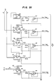
- the operation of the supervisory circuit 3 can best be understood by understanding the operation of the resident program, which prioritizes the application of the parallel data signals to the TIS 6 and VPS 8, shown in simplified form in Fig. 3.
- the prioritizing of the parallel data provides efficient transmission to the TIS 6 and VPS 8, with the T1S 6 and VPS 8 generating parallel data such as line-ringing and other status data which is translated by the supervisor 3 into standard serial data, as described previously, recognizable by the host computer 2.
- the supervisor 3 also prioritizes the transmission of the standard serial data to the host computer 2, as will be described in more detail hereinafter.
- the program upon powerup 27, the program directs a diagnostic check of the circuitry 28. Upon successful completion of the diagnostic check, the program directs a check on which of the telephone lines are active 29.
- the VoiceTek Model 50 TIS 6 for instance, can be configured to interface with from 2 to 32 telephone lines 10 (in multiples of 2).
- the program determines if the line 10 position is active.
- the program creates a table or "map" of the configuration of the TIS 6 which it places in RAM 26.
- the program Upon completion of the TIS 6 map at 29, the program begins a loop, which, with the exception of certain interrup- tons (described below), will continue indefinitely.
- This loop may be set up in a number of different ways to service the tasks which must be performed; different methods of programming the loop will address the same tasks, but will address them more or less frequently, depending on the details of the program.
- the system described in Fig. 3 is an example of a loop which works well with the VoiceTek Model 50 TIS 6 and VoiceTek Model 30 VPS 8.
- the program polls each of the active telephone lines in turn, performing several tasks at each step. Then, before returning to poll the first telephone line again, the program will perform several other tasks. Typically each polling step will require 100 microseconds; if the full compliment of 32 telephone lines is to be serviced, the entire loop will therefore take 4 milliseconds. Thus some tasks are performed relatively often (every 100 microseconds) and some tasks are performed less often (every 4 millisecond). By choosing the correct mix of frequently performed tasks and less frequently performed tasks, system performance can be optimized.
- the program When the program begins by polling the first active telephone line 10 at 30, it first performs the task of transmitting waiting messages to the host computer 2 at 31. (Both the VPS 8 and the TIS 6 generate messages for the host computer 2). All communication from the VPS 8 to the supervisor 3 is accomplished by the introduction of an interrupt.
- the interrupt causes the program to break out of the loop shown in Fig. 3 between steps 30 and 36 and to execute a routine which serves the VPS 8 and then returns control to the program of Fig. 3 at whatever point the interrupt broke in.
- This routine causes the microprocessor 12 to read the message from the VPS 8, translate it into a text string for transmittal to the host computer 2, and store the message in RAM 26.
- the TIS 6 also generates messages for the host computer 2, for instance messages relating to the status of various timers and messages relating to the status of the telephone lines 10 (see below). In the normal course of the polling program, these messages are translated into text strings and placed in RAM 26 awaiting transmission to the host computer 2, along with the messages from the VPS 8.
- All VPS 8 and TIS 6 messages for the host computer 2 are maintained in a RAM 26 area called the "host command queue".
- the first character waiting in the queue if any, is sent to the host computer 2.
- the next and subsequent characters are sent upon the next and subsequent iteration of the polling program).
- timing registers are controlled by a timing routine 32.
- register clocks are controlled by a master clock. Since the times of interest for control are never controlled with greater precision than a few tenths of a second, the master clock has a very long period, typically 30 milliseconds. Thus the program generally cycles through several polling cycles within a single master clock cycle.
- the master clock is used to force a change of state in a one-bit register each cycle.
- the register clocks are updated by the program, which looks at the one-bit register and determines if it has changed its state since the last iterative pass. If it has, the program increments the contents of the three registers which are timing activities for the phone line 10 which the program is currently servicing.
- the register clocks may be used for various purposes, depending upon the application.
- the first clock is reset and begins running when a request for service on the phone line 10 is answered, that is, when the line 10 goes off-hook. It is reset upon any subsequent command activity on the line 10. It thus times periods of inactivity.
- the program will read the register and report to the host computer 2 each time the register has recorded some established increment of time, for instance ten minutes. If thus warns the host computer 2 that an unreasonable amount of time has passed without activity on the line and the transaction should probably be terminated.
- the second clock is reset and updated when a request for service on the phone line 10 is answered, that is, when the line goes off-hook. It continues to record time until the calling party has supplied appropriate information, as by touch-tone signals (typically his subscriber number and the code designating the type service the customer wants). After incrementing the clock, the program reads the register and if the required information does not appear within some preset time (say thirty seconds),the program informs the host computer 2, which can then initiate a voice message prompt for the missing information or hang up the line 10.
- the third clock controls the interval during which one of the telephone signaling tones is placed on the line 10 at the command of the host computer 2.
- the tone generator 21 for the beep will be actuated and the third clock will be reset and updated.
- the program will read the register after each increment until the preset time for the "beep" elapses; the program will then turn the tone off.
- All communication from the host computer 2 to the supervisor 3 is accomplished by the introduction of an interrupt
- the interrupt causes the program to break out of the loop shown in Fig. 3 and to execute a command to message system from TIS routine 33 which serves the host computer 2 and then returns control to the program of Fig. 3 at whatever point the interrupt broke in.
- This command routine 33 causes the microprocessor 12 to determine whether the command is intended for the TIS 6 or the VPS 8 and writes the appropriate translation of the command into a preassigned area of RAM 26 for transmittal to either the TIS 6 or VPS 8 as previously described.
- the polling program determines whether the line 10 currently being polled is calling for service (a ring on the line 10), if the calling party has hung up, the most recent digit recorded by a touch-tone decoder, and so forth. These messages are translated and placed in the host computer 2 command queue, described previously, at this point in the polling program.
- the program now checks to see if it has reached the last active line at 34; if not, it considers the next active line at 35 and repeats the tasks described above. If the last active line has been served, however, noted at 34, before returning to the first line at 30 some additional tasks are performed. These tasks, called a less frequent routine 36, may have many functions such as a command to VPS 8 routine and the activation of a fourth timing clock, as described in more detail below.
- commands from the host computer 2 to the TIS 6 or VPS 8 may appear at any time in the assigned area of RAM 26 as a consequence of interrupts.
- the memory space assigned to commands intended for VPS 8 is checked to see if there are any commands. If there are any, they are executed at this point by putting them on the data bus 14 to the VPS 8.
- the fourth clock controls the off/on time for telephone signaling tones which require interruption, for instance the busy tone and the ringing tone. This clock runs continuously. The program will examine the register after each increment and will turn the tone off or on as appropriate whenever the time exceeds a preset amount.
- DMA direct memory access
- Transfer operations may be programmed in various ways, depending on the character of the VMX 8.
- the VoiceTek Model 30 transfers data in 6K bytes.
- the system of Fig. 4 when used with a model 30 as a VMX 8, is designed to handle data in 6K batches.
- a second RS 232-C port may be used. which exists on many host computers 2, as well as on the UART 19 chip used in the example supervisor 3. By dedicating this second data channel to disk-to-disk transfers, such operation may be carried out as time permits, without disturbing the normal operation of the system 1. Such operattons are termed "operations in the background.”
- data including status data
- data is cached in the supervisor 3 RAM 26 in the process of transfer.
- Voice data from the host computer 2 is translated into a compatible 6K byte text string representation, sent over the second RS 232-C line, and cached in the supervisor RhM 26.
- the 6K byte of voice data is transferred to the VPS 8 under control of the direct memory access device 37. This process is continued until the complete message has been transmitted.
- the transmittal of voice data from the VPS 8 to the TIS 6 over lines 11 is therefore accomplished under the control of the direct memory access device 37 in passing 6K byte batches to the supervisor RAM 37 cache. Such data is then translated into text string representation and passed to the host computer 2 through the second RS 232-C channel. Such a method can also be used to transfer extended command strings.
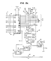
- Fig. 5a shows a typical realization of the circuitry for the UART 19 which communicates with the host computer 2.
- the UART 1 9 illustrated is the Z80A SIO/O, a device which is designed to interface with most commonly used microprocessors 12, such as the Z80A (see Fig. 5b).
- the UART 19 supports communication lines 4, shown as two RS 232-C lines 38 and 39, to the host computer 2; line 38 is used for command and information exchange with the host computer 2, and 39 is used for disk-to-disk transfers as described previously, or other transfers of large blocks of data.
- Some signal conditioning may be required on lines 38 and 39 depending on the nature of the RS 232-C ports available on the host computer 2 and the length of the connecting lines 4.
- the two device ports of the UART 1 9 are labeled "A" corresponding to line 38 and "B" corresponding to line 39.
- Each has four lines: TXD, RXD, RTS and CTS.
- the TXD line carries data being transmitted from the supervisor circuit 3 to the host computer 2 in the RS 232-C serial format and corresponds to the transmit line 17 in Fig. 2.
- the RXD line carries data being transmitted from the host computer 2 to the supervisor circuit 3 and the RS 232-C serial format and corresponds to the receive line 16 in Fig. 2.
- Each port A and B also has two control lines; RTS (request to send) and CTS (clear to send), corresponding to the control lines 1 8 in Fig. 2.
- the RTS terminal is normally high, indicating that the device can accept signals from the host computer 2. If the internal buffer of the UART 19 is filled, this RTS terminal will be switched to a low signal, warning the host computer 2 not to send another character until space is available and the RTS terminal is switched to high.
- the host computer 2 can warn the UART 19 not to send characters to it by supplying a low signal on the CTS line, which is otherwise maintained in the high state by the host computer 2.
- the PTS and CTS terminals are used to control the flow of information between host computer 2 and supervisor circuit 3 according to the RS 232-C protocol.
- the data bus 14 consists of the data lines DO through D7. This data bus 14 will contain a character which is to be sent to the host computer 2 (in parallel format) or win have impressed on it a character being transmitted by the host computer (in parallel format) to the supervisor circuit 3. These characters are generated and used as described previously in reference to the VPS 8, TIS 6 and the timing routine 32.
- the UART 19 requires two clock signals.
- the first carried by timing line 41, originates from the master clock 42 used to operate the microprocessor 12 (see Fig. 5b); being used to synchronize the operation of the UART 1 9 with that of the microprocessor 12.
- the clock signal is sharpened by the push-pull transistor amplifier 43 using transistors 44 and 45 and their associated circuitry. This clock signal is then applied to the CLK (clock) terminal " of the UART 19.
- the second clock signal establishes the speed at which bits are transferred between the host computer 2 and UART 19. Preferably the highest standard speed for transfer possible is used, this rate being approximately 1 9.2 kHz.
- This signal carried by timing line 46, is derived from the tone generating portion of the supervisor circuit 3, shown in Fig.
- the frequency imposed on the first divider 48 is 4.9152 mHz.
- the frequency supplied to the UART 19 (which is further divided within the UART 19) is one-fourth this value, that is 1.2288 mHz, to establish a 19.2 kHz transfer rate. Further division reduces the value of the signal on line 53 to 37.5 Hz (27 msec period).
- the RST (reset) terminal of the UART 19 is driven low to place the device in an initial operating mode when power is applied or when a reset push button is actuated; the reset circuitry being discussed in greater detail in connection with Fig. 5B. Under normal operation this terminal is held high.
- Line 54 IEO (interrupt enable output), line 55 INT (interrupt), and line 56 IEI (interrupt enable input) connections to the UART 19 are used to interrupt the microprocessor 1 2 and to establish the priority of the UART 19, automatically generating an interrupt (INT terminal goes low) whenever the host computer 2 sends a character. This interrupt signal is then carried by line 55. As discussed in more detail in connection with the DMA 37 circuit shown in Fig. 5g, a brief delay may occur before this character can be processed if the higher priority DAM 3 7 has established its priority by driving the IEO low on line 56. Interrupts from the UART 19 take priority over those generated by the VPS 8 and the TIS 6, however, as established by the connection of the IEO line 54 from the UART 19.
- the RD (read) terminal of the UART 19 is held low if the device is to read data from the date bus 14; it is held high if the UART 14 is to write data to the data bus 14.
- the origin of the signal is the microprocessor 12 (shown in Fig. 5b and carried through bus 58 in Figs. 5c and 5d).
- the IORQ (input/output request) terminal of the UART 19 is driven low by the microprocessor 12, carried along bus 58, and line IORQ addresses an input/output device rather than the memory. When this IORQ line is low, the CE (chip enable) signal can activate the UART 19 as discussed below.
- Line 57 CE (chip enable) connection to the UART 19 allows the UART chip 19 to read data from the data bus 14 and place data on the data bus 14 only when addressed by the microprocessor 12; the origin of the signal being the address bus 23 of the microprocessor 12, decoded as described in connection with Fig. 5d.
- the B/A terminal of the UART 19 causes the device to recognize either port A (low signal applied) or port B (high signal applied).
- the signal is carried on line A1 of the address bus 23 of the microprocessor 12, as shown in detail in Figs. 5b and 5d.
- the C/D terminal of the UART 19 causes the device to interrupt signals on the data bus 14 as data (low signal applied) or as commands to the UART 19 from the microprocessor 12 (high signal input).
- the signal line AO of the address bus 23 of the microprocessor 12 carries the signal, as shown in detail in Figs. 5b and 5d.
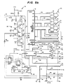
- Fig. 5b a typical realization of the circuitry for the microprocessor 12 used in the supervisory circuit 3 is shown.
- the Z80A microprocessor 12 uses a 16 line address bus 23.
- the address bus 23 is split into two buses, the first address bus 59 contains address lines AO through A7 and the second address bus 60 contains address lines A8 through A15.
- Both address buses 59 and 60 are passed directly to the DMA 37 (Fig. 5g) and, via the permanently enabled line drivers 61 and 62 to the decoding circuitry described in connection with Fig. 5c.
- control terminals (MI, MREQ, IORQ, RD, WR, and REF, discussed briefly above) of the Z80A microprocessor 12 are formed into a control bus 58 and passed directly to the DMA 37 (Fig. 5g) and, via permanently enabled line driver 63, to the other circuits of the supervisor circuit 3 as shown in Figs. 5c, 5d, etc.
- the six signals in the control bus are:
- MREQ memory request
- IOREQ input/output request
- RD (read) This output provides a (low) signal when the program causes the memory location or device addressed to read the contents of the data bus 14.
- WR (write) This output provides a (low) signal when the program causes the memory location or device addressed to write information to the data bus 14.
- REF Refresh: This output provides a (low) signal to allow dynamic memories to undergo the refreshment process. Dynamic memories are not used in the illustrated circuitry; the signal being used only to disable operation during the time that the microprocessor 12 has set aside for the refreshment process.
- the BUSACK and BUSRQ (bus acknowledge and bus request) signals are used in connection with the operation of the DMA 37 described in connection with Fig. 5g.
- the microprocessor 12 Upon receiving a low signal on the BUSRQ line the microprocessor 12 turns the supervisor circuit 3 buses 14 and 23 over the the control of the DAM 37 and acknowledges this action by providing a low signal on the BUSACK line.
- the Z80A microprocessor 12 uses an 8 line data bus 1 4 .
- the data bus 14 is passed directly to the DMA 37 ( Figure 5 g) and, via the bus connector device 15, to the rest of the supervisor circuit 3.
- the bus connector 15 can isolate the two sections of the data bus 14 which it connects if the EN (enable) input is high, or depending on the setting of the DIR (direction) input, can pass data in one or the other direction along the sections of the data bus 14 which it is connected to if the EN input is low.
- the EN signal for the bus connector 15 is derived from the not gate 64 and carried on line 65 which, in tum, is driven from a decoded address signal carried on line 66 from a decoder 68 shown in Fig. 5d.
- the same decoded address signal is passed by line 67 to the chip enable terminal (CE) of the DMA 37 (Fig. 5g) which also requires a low signal to operate. Because of the inversion produced by the not date 64, however, the bus connector 15 is open whenever the DMA 37 is actuated and passes data to the rest of the supervisor circuit 3 only when the DMA 37 is not enabled.
- the correct direction of data flow is established by the DIR signal carried by line 70 to the bus connector 15, received from the gate 69 which is in turn driven by the Mi and RD signals from the microprocessor 12 as discussed above, and shown routed through bus 58 in Figs. 5b and 5c.
- the INT (interrupt) signal may be applied to the microprocessor 12, along the 71, by the DMA 37 (Fig. 5g), by the UART 19, (Fig. 5a) by the VPS 8 or by the TIS 6, in that order of priority.
- the microprocessor 12 receives an interrupt signal (INT low), it looks on the data bus 14 to find the address of the appropriate program routine to service the interrupt. The method of establishing the interrupt priority and placing the interrupt vector on the data bus 14 is described in connection with Figs. 5a - 5g describing each of the devices, respectively.
- the INT signal itself is derived from and gate 72 the output of which is pulled high by the connection to the 5 V line 73.
- the and gate 72 is driven by lines 55 and 74.
- the signal on line 55 is generated by the INT output of the DMA 37 (Fig. 5g) or by the INT output of the UART 19 (Fig. 5a); the signal on line 74 is generated by the INT output of the VPS 8 or the INT output of the TIS 6, as discussed hereinafter (Fig. 5d).
- Polarities and logic are set so that if any of the four devices (DMA 37, UART 1 9, VPS 8 or TIS 6) generates an interrupt signal, it will drive the INT input of the microprocessor 12 low, thus initiating the interrupt process. Note, however, that the priority setting system prevents more than one device from simultaneously supplying an interrupt signal.
- the reset circuitry 75 causing a reset (RST) signal, is actuated by pushbutton 76 or in the process of applying power to the supervisor circuit 3; the RST signal is cleaned by the not gates 77 and applied to the RST (reset) terminal of the microprocessor 12 and passed to other circuitry requiring a reset signal (Figs. 5a and 5c) by line 89.
- RST reset
- the clock signal (CLK) for driving the microprocessor 1 2 is derived from a crystal controlled oscillator 78 of the masterclock 42 using not gates 79 and 80 as active elements.
- the CLK signal is cleaned, sharpened, and isolated by flip-flop latches 8 1 , not gate 82, and the push-pull amplifier 83 which uses transistors 84 and 85 as active elements.
- the desired operating frequency for the microprocessor 12 is 4 mHz, therefore, because the flip-flop latches 81 divide the signal by four, the oscillator 78 is operated at a crystal frequency of 16 mHz.
- the 4 mHz clock signal (CLK) is also passed to the delay circuit 86 by line 87, as described in connection with Fig. 5c, to the UART 19 (Fig. 5a) by line 41 through isolating not gate 88, and to the DMA 37 (Fig. 5g) by line 90.
- Fig. 5c shows the memory circuit
- ROM 13 read only memory
- RAM 26 random access memory
- Two memory chips are used for ROM 13, each one being organized as an 8K x 8-bit device, and four memory chips are used for RAM 26, each also being organized as an 8K x 8-bit device.
- the data terminals DO-D7 of each memory device 13 and 26 are attached directly to a segment of the central data bus 14.
- the address terminals of the memory chips 13 and 26 are all attached to the first address bus 59 containing address lines AO through A7 and to the first five lines of the second address bus 60, being address lines A8 through A 1 2.
- the active memory chip 13 or 26 is sejected by driving the CS (chip select) and OE (output enable) terminals of the selected memory chip low, using signals from decoders 91 and 92. These decoders 91 and 92, in turn, are driven by signals from address lines A12 through A15 of address bus 60.
- the decoders 91 and 92 are also used to deactivate memory circuits during the refresh cycles by a signal from the REF line of bus 58 applied to terminal G1 of decoder 91 and, by way of not gate 93, to terminal G2B of decoder 92.
- the memories 13 and 26 are only active if a low signal is placed by the microprocessor 12 on the MREQ line in bus 58.
- the ROMs 13 are activated by the MREO signal applied to terminal G2B of decoder 91.
- the RAMs 26 are activated by the MREQ signal applied to terminal CS2 (chip select 2) of RAMs 26 by the logic circuit formed by gate 94 and not gate 95. Additionally, the RAMs 26 are instructed to read or write by a signal applied to their RD/WR (read/write) terminals by or gate 96 which, in turn, is driven by the WR line of bus 58 in coincidence with the MREQ signal discussed above.
- the delay circuit 86 formed by not gates 97 and 98, or gates 99, 100 and 101, and flip-flop latches 102 and 103 is driven by signals Ml, IORQ, WR, and the 4 mHz microprocessor 12 clock signal 87.
- the delay circuit 86 introduces a slight delay in the writing of data to the T1S 6 and VPS 8 through the signals carried on lines 104 and 105 as explained in connection Figs. 5d and 5e. The delay allows the data signal to settle, to a void interference, before it is clocked into the assigned memory location.
- the VPS 8 interface circuitry shown in Fig. 5d requires address lines AO through A6 on address bus 59 and an inverted signal from the signal carried on address line A7 on address bus 59.
- the inversion on line A7 is produced by not gate 106 supplying address line 107, as shown in Fig. 5c.
- the RD, IORQ and MI lines are also supplied to the VPS 8 interface circuitry shown in Fig. 5D, for use as described below.
- the Mi and RD lines are also supplied to the bus connector 15 circuitry shown in Fig. 5b as described previously.
- Fig. 5 d shows a detailed realization of the required circuit interface with the VoiceTek Corporation Model 30 VPS 8.
- the Model 30 exchanges control information (not to be confused with the audio signals which it processes) by means of an 8-line control bus 108 driven by a permanently enabled line driver 109, an 8-line data bus 7, a data ready line 111, a buffer ready line 112, and a reset line 113, discussed in more detail hereinafter.
- VPS 8 control bus 1 08 lines are designated 108a through 108h. They have the following functions and are generated by the supervisor circuit 3 in the following ways:
- Line 108b RDDSEL read data select: Read signals are developed when the VPS 8 wishes to pass data to the host computer 2 through the supervisor circuit 3. A low RDDSEL signal must coincide with the RD signal (line 108h, see below) to allow the VPS 8 to place data on the data bus 7 for the host computer 2 to read.
- the RDDSEL signal is generated by the decoder 1 14 which decodes the first three lines A0, A1 and A2 of the address bus 59.
- Line 108c DATACK (data acknowledge): The supervisor circuit 3 drives this line low in coincidence with a WR signal (line 108g, see below) to indicate to the VPS 8 that a complete command/data string has been received.
- the DATACK signal is generated by the decoder 114 which decodes the first three lines A0, A1 and A2 of the address bus 59.
- Line 108d SERREQ (service request): The supervisor circuit 3 drives this line low in coincidence with a WS signal (line 1 08g, see below) to indicate to the VPS 8 that the end of a command/data string from the host computer 2 has been reached.
- the SERREQ signal is generated by the decoder 114 which decodes the first three lines A0, A1 and A2 of the address bus 59.
- Line 108e WRSYNC (write sync): The supervisor circuit 3 drives this line low in coincidence with a WS signal (line 108g, see below) to indicate to the VPS 8 that a command/data string is about to be transmitted.
- the WRSYNC signal is generated by the decoder 114 which decodes the first three lines A0, A1 and A2 of the address bus 59.
- Line 108f RDSYNC read sync: The supervisor circuit 3 drives this line low in coincidence with a WS signal (line 108g, see below) to syncronize a command/data string before it is read.
- the signal is generated by the decoder 114 which decodes the first three lines A0, A1 and A2 of the address bus 59.
- Line 108g WS (write strobe): This low signal is carried by line 105 and generated by the delay circuit 86, as described in connection with Fig. 2c, to enable the placement of data.
- Line 108h (read) This low signal is the read signal generated by the supervisor circuit's microprocessor 12 and carried on line RD via Fig. 5c (see the description provided in connection with Fig. 5b).
- the VPS 8 data bus 7 gains access to the supervisor circuit's data bus 14 through bus connector 15.
- the direction of data flow is determined by the presence or absence of the RD signal from the microprocessor 12.
- the bus connector 15 is enabled by a signal carried on line 1 15 from decoder 11 6, which decodes address lines A3, A4 and A5 of address bus 59.
- Line 1 11 DATRDY (data ready) provides a low signal from the VPS 8 signifying that it is holding a command/data string in its buffer to be transferred to the supervisor circuit 3. As indicated previously, such transfers are made by an interrupt.
- the DATRDY signal is placed directly on line D1 of the data bus 14 when line driver 1 17 is enabled by a signal from or gate 118 which, in turn, is actuated by the RD line and a signal carried on line 119 from decoder 68, decoding address lines AO and A1 of address bus 59.
- Line 111 carries an interrupt signal and it is also applied to the second half of line driver 117.
- This half of the line driver 117 is always active and generates the interrupt by driving not gate 120 and flip-flop latch 121 which, in turn, drives the decoder 122.
- the decoder 1 22 generates a signal, carried on line 74 to interrupt the microprocessor 12 (as described in connection with Fig. 5b) and also places a vector for the interrupt routine on the data bus 14 through line driver 123.
- gate 110 resets flip-flop latch 121 when activated by signals from the write strobe WS signal carried by line 105 and from decoder 114.
- Line 112 carries a BUFRDY (buffer ready) low signal from the VPX 8 when its buffer is ready to receive a command/data string from the supervisor circuit 3.
- This BUFRDY signal is placed directly on line D2 of the data bus 14 when line driver 117 is enabled by a signal from or gate 118 which, in turn, is actuated by the RD line and a signal carried on line 119 from decoder 68, decoding address lines AO and A1 of address bus 59.
- Line 113 carries a RESET (reset) signal to the VPS 8 through line driver 117.
- the RESET signal is generated by or gate 124 which is driven by the write strobe WS signal carried by line 105 and a signal carried on line 125 and generated by the decoder 114 which decodes three address lines A0, A1 and A2 of the address bus 59.
- the interrupt routine described above can be initiated by a signal from the TIS 6 carried on line 126 from the TIS 6 (in case a data transfer can be accomplished more efficiently by interrupt rather than by the polling process described previously). Because decoder 122 generates a different signal when an interrupt is produced by the TIS 6, a different vector is placed on the data bus 14, directing the microprocessor 12 to a routine suitable for serving a TIS 6 interrupt. The connections therefore establish the priority of the VPS 8 interrupt over the TIS 6 interrupt.
- Line 5 4 derives from the UART 19 (described in connection with Fig. 5a) and the signal it carries establishes the priority of UART 19 interrupts over interrupts from the VPS 8 and the TIS 6 by virtue of its connection via not gate 127 and line 40 to decoder 122 and via or gate 128 to line driver 123, which is also controlled by not gate 129 in response to the IORQ and Mi signals generated by the microprocessor 12.
- the 3 7 .5 Hz clock signal carried on line 53 described in connection with Fig. 5a is placed on line D2 of the data bus 14 through the gated section of line driver 117.
- Other connections shown in Fig. 5d are provided to gate the various decoders and other devices to operate only at appropriate times in the program cycle.
- Fig. 5e shows the interface between the supervisor circuit 3 and the telephone interface system (TIS) 6; the circuit shown is appropriate for connection to the VoiceTek Model 50 TIS 6.
- TIS telephone interface system
- the Model 50 can handle up to 32 telephone lines. In order to initiate inquiries on the status of a telephone line the model 50 expects the supervisor circuit 3 to address the telephone line in question.
- the telephone lines are divided into two groups of sixteen.
- Address line A6 on bus 59 of the supervisor circuit 3 is used to designate which group of telephone lines is to be addressed.
- the particular telephone line is then designated by signals as described below.
- the signal on line A6 is high, the first group of 16 telephone lines is enabled; when the signal on line A6 is low a high signal is developed by not gate 130 which enables the second group of 16 telephone lines.
- a specific telephone line is selected by signals carried on the two 8-line buses 131 and 1 32.
- Supervisor circuit 3 address bus lines A2 through A5 carried on bus 59 are used to address the individual telephone lines; the signals carried by those lines are decoded by decoders 133, 134 and not gate 135.
- the 8-line buses 136 and 137 carrying the decoded signals are supplied to the 8 line busses 131 and 132 and then to the TIS 6 by the two permanently enabled line drivers 138 and 139.
- Bus 140 and bus 141 transfer commands to the TIS 6.
- Bus 140 passes the signal contents of lines D4 through D7 of the data bus 14 through the first half of line driver 142; these lines actuate off hook, reset digit/ring, on hook, and trunk reset signals for the telephone line addressed.
- the line driver 1 42 is enabled by a signal carried on line decoded by decoder 143, which is actuated by lines AO and A1 of the supervisor circuit 3 address bus 59.
- Bus 140 also contains a line to the trunk strobe of the Model 50 Tls 6; this signal is derived from decoder 143 and is applied through the second half of line driver 14 2 by line 1 4 6 when the line driver 142 is enabled by the write strobe signal carried by line 105.
- Decoder 143 is in turn enabled through or gate 147 driven by line 104 and by line 107.
- Bus 141 passes the contents of lines DO through D3 of the data bus 14 through permanently enabled line driver 148. These lines DO through D3 actuate VPS-0 through VPS-4, assigning one of the various voice paths that the TIS 6 can employ.
- the bus 141 also contains a RST (Reset) line to reset the Tis 6 and the address lines described above (A6 and inverted A6).
- the signals, eight in number, are as follows: the first four are BCD (binary coded decimal) representation of decoded touch-tone signals on the telephone line; the others, in order, are a hook change signal, an off hook signal, a digit assembled signal, and a trunk identification signal.
- Line driver 1 50 is enabled through or gate 151 by a signal carried by line 152, decoded from address bus lines AO and A1 by decoder 143 and by the RD signal.
- Lines DO and D1 of the supervisor circuit 3 data bus 14 are used to clock the tone circuits which require interruption (see below). They are passed to the tone generator circuit (see Fig. 5f) by line driver 153 which is enabled by a signal carried on line 154 from decoder 143 via line 144 when the write strobe signal carried on line 105 enables line driver 1 4 2.
- Fig. 5e also shows one of the bus connectors 15 used to establish the flow of data on the supervisor circuit's data bus 14.
- the bus connector 15 is enabled by the MREQ signal; direction is established by the RD signal.
- the gating circuits of the decoders 143 and 134 are connected through line 104 to enable these circuits at the proper program segments, which may also include the connection through rot gate 135.
- Fig. 5f shows the tone generating circuit
- the TIS 6 will place one of four telephone tones on a telephone line's audio circuit a diai tone, a busy tone, a ring tone, or a valid tone. These tones are generated by the supervisor circuit 3 and passed to the TIS 6, as described generally, previously. The tones are generated by tone generating chips 155 using appropriate crystals 156 to establish the appropriate audio frequencies.
- the lines to the TIS 6 are driven by operational amplifiers (op. amps) 157.
- the tones requiring interruption (busy and ring) are interrupted by signals placed on a segment of the data bus 14 as described above.
- the crystal 155 which establishes the frequency of the valid tone is also carried by line 46 and used to feed the clock circuit described in connection with Fig.
- the direct memory access (DMA) circuit is shown in Fig. 5g.
- the circuit consists of a single DMA chip 37; the Z80A DMA is illustrated.
- the DMA chip 37 is used to enable disk-to-disk or other bulk data transfers in the background of supervisor circuit 3 operation as described previously. Connections to the DMA chip 37 include the supervisor circuit address buses 59 and 60, control bus 28, and data bus 14. It should be noted that one line of the control bus 28, the REF line, is not required by the DMA chip 37.
- the DMA chip 37 functions by taking over control of the supervisor circuit buses 14, 58, 59 and 60 from the microprocessor 12; it then transfers data between I/O devices and memory without the intervention of the microprocessor 12, thereby speeding such transfers. It requests bus control by driving line the BUSRQ line low; this line is connected directly to the BUSRQ input of the microprocessor 12, as described previously. After transferring control of the buses 14, 58, 59 and 60 to the DMA 37, the microprocessor 1 2 places a low signal on its BUSACK (bus acknowledge) output; this signal is passed directly to the BA1 input of the DMA chip 37.
- the DMA chip 37 also requires a clock input the CLK signal used by the microprocessor 12 is also passed to the CLK (clock) input of the DMA 37.
- the DMA 37 interrupts operation of the microprocessor 12 by placing a low signal on line 55; the DMA chip 37 can then place a vector to the appropriate routine on the data bus 14 .
- the priority of DMA 37 interrupts is established by holding the IEO (interrupt enable output) of the DMA 37 high at all times.
- the IEO of the DMA 37 is connected by line 56 to the IEO input of the UART 19.
- Operation of the DMA 37 is enabled by a low signal on line 67 to the CE (chip enable) input of the DMA 37; this signal is derived (via Fig. 5b) from a decoder 68 circuit described in connection with Fig. 5d. Finally, the RDY (ready) input of the DMA 37 is actuated by line 54 from the IEO (input enable output) of the UART 19 to prevent overflow of the UART 19 buffer when the DMA 37 is active.
Abstract
Description
- The present invention relates to a method for controlling digital audio recording and playback systems designed for connection to telephone lines, being more particularly directed to a controller or supervisor used in connection with a host computer, a telephone interface system and a voice processing system for receiving and sending digitized recordings from and over a telephone line.
- Recording and playback of voice messages is often useful in business applications. This capability is useful for order entry systems, for dictation for subsequent transcription, for obtaining spoken output from a computer data base, or simply to take the place of written communications in the transmittal of information. Numerous methods have been proposed to satisfy this need. The present invention relates only to digital voice messaging systems.
- In the recording mode, the digital voice system such as shown in U.S. Patent 4,371,752, first produces a digital signal which represents the audio message signal; this stream of digital data is then recorded on a digital memory, such as a magnetic disk recorder ("Winchester" disk). In the playback mode, the Winchester disk is accessed for a particular message, the message is converted into a stream of digital data which is, in turn, converted to an audio signal. Because such a system operates at very high speed, up to 32 lines of recording and playback can be simultaneously accommodated without the introducion of delays which are perceptible to the users.
- A common source of audio messages for recording and a common method of accessing messages for playback is a telephone line. The lines may be part of the public switched telephone network or they may be a part of a business telephone system under the control of a private branch exchange (PBX) in the business premise. However, prior systems required a custom or specific dedicated host computer, directly connected by a parallel bus device to all input/output, processing and memory hardware to provide the needed operational speed discussed above. Changes in the system, such as necessitated by increased message mode on the system, that would require a change in the capacity or type of host computer, could therefore not be accomplished without re-designing the entire system, or at least the intemal communications bus system, to satisfy the communications protocol of the new computer. Additional, the dedicated custom computer of prior bundled systems may lack flexibility to handle other processing needs and may not be suitable for the general needs or other needs of the user as well as expanded voice messaging needs.
- The present invention relates to an unbundled system, whereby any host computer can be connected to the telephone lines and the voice storage and playback means and may be controlled by outside means (usually by a host computer) to provide a system which can be used for the purposes described above and other purposes. Such un- bundling, or severing of the bus-connected custom system would normally entail a loss of efficiency and speed. However, the present invention provides for a general purpose host computer to be easily connected to a standard telephone line interface and a standard voice processing system without sacrificing speed or efficiency. Such connection is facilitated by a novel electronic communications supervisor that provides distributed processing from the host computer and allows for the utilization of any standard host computer as a voice messaging system controller, without substantial system re-design to facilitate changes in the computer.
- Therefore, it is an object of the present invention to provide a novel electronic communications supervisor for connection to a host computer, telephone line interface system and voice processing system that is not subject to prior limitations but instead allows for any standard host computer to be used as a voice messaging controller without loss of speed or efficiency.
- Another object is to provide a novel electronic communications supervisor that provides distributed processing control functions to release the host computer from such functions.
- Other and further objects will be explained hereinafter and are more particularly delineated in the appended claims.
- In summary, from one of its important applications, the invention embraces an electronic communications supervisor for controlling digital recording and playback of voice messages for connection to a telephone line interface, a voice processor and a host computer, having, in combination, electronic digital signal processing means for controlling the operation of the supervisor; parallel means for receiving and transmitting digital control signals between the telephone interface and said electronic digital signal processing means to provide access to the telephone lines for voice messages; parallel means for receiving and transmitting digital control signals, for controlling voice messages, between the voice processor and said electronic digital signal processing means; analog audio lines for transmitting voice messages between the telephone line interface and the voice processor under control of the electronic digital signal processing means; audio processing means associated with the voice processor for converting said voice messages into the digital data signals representing voice messages and from digital data signals representing voice messages into voice messages, digital memory means controlled by said electronic digital signal processing means for storing said digital control signals, digital memory means controlled by said voice processor for storing digital data representations of the voice messages; means for storing in said memory means said digital representations of the voice messages from said voice processor; and serial means for receiving and transmitting digital control signals and said signals between the host computer and the electronic digital signal processing means. Other inventive features and preferred constructional details are hereinafter described.
- The invention will now be described with reference to the accompanying drawings:
- Fig. 1 of which is a schematic drawing of a voice messaging system having a universal supervisor circuit connected to a host computer, a telephone line interface and a voice processing system;
- Fig. 2 is a more detailed schematic, similar to Fig. 1, showing the universal supervisor circuit of the present invention;
- Fig. 3 is a flow chart of a standard processing routine used by the supervisor; and
- Fig. 4 shows a direct memory access in the supervisor to facilitate the transfer of digitized voice messages or long commands to and from the host computer.
- Figs 5a-5g are the schematic drawings of a preferred circuit of the present invention.
- Referring now to Fig. 1, a
voice messaging system 1 having ahost computer 2 is connected to auniversal supervisor circuit 3 byserial communication lines 4; thesupervisor circuit 3 is connected, in turn by a parallelbus communication line 5 to a telephone interface system (TIS) 6 and by a parallelbus communication line 7 to a voice processing system (VPS) 8 with associated Winchesterdisks 9. In the typical application, up to 32telephone lines 10 are connected to theTIS 6 which is connected to up to 32 audio signal lines 11 to theVPS 8 as will be described in more detail hereinafter. - The
host computer 2 may be any type of machine which can exchange information using a standard serial protocol, such as RS 232-C, an attribute of almost all computers. Thehost computer 2 operates using a program which is designed to handle the particular application for which the system is intended. Thesupervisor 3 will store commands from thehost computer 2 and commands tailored to command and control theTIS 6 andVPS 8 and translate such commands and data into a command and control language recognizable by theTIS 6 andVPS 8 and convert the translated language into parallel data signals, as will be described in detail hereinafter. - The TIS 6 provides a telephone line connection which meets the requirements of the Federal Communications Commission designed to protect the public switched network such as the
model 50 sold by VoiceTek Corporation, Newton Massachusetts. The TIS 6 contains no 'intelligence'; it simply serves to answer thetelephone line 10 when thetelephone line 10 calls for service (for instance, by imposing a ringing signal) by providing an audio path along lines 11 to thevoice processing system 8. It is also capable of collecting and providing various signals to thetelephone lines 10 provided by or required by a switched network, such as a PBX or Central Office, to establish and maintain such an audio path. The nature of these signals depends on the type of telephone lines; for the simplest type of line, a subscriber loop for instance, thetelephone interface system 6 answers a ring by providing a low DC resistance across theline 10. The switched network interpret this as an "off hook" condition; that is, someone has answered the telephone. The ringing signal is tripped off the line at the switched network's central office or PBX and an audio connection may proceed. All of these actions on the part of thetelephone interface system 6 are controlled by thehost computer 2, as such status data representing actions are sent between theTIS 6 and thehost computer 2, however; none are initiated by thetelephone interface system 6 itself. - The
voice processing system 8, such as themodel 30 sold by VoiceTek Corporation, may have considerable internal 'intelligence' related to the processing of the analog audio signals carried on line 11 and digital signals but it also relies on control signals, such as those sent in standard serial data format from thehost computer 2, to function; it must be told which line 11 to service, whether the service involves recording or playing back a message; and identification of the message itself by the host computer. - The
supervisor circuit 3 handles the interface between thetelephone interface system 6, thevoice processing system 8 and thehost computer 2. Thesupervisor 3 also provides a considerable intelligence which would otherwise require extensive programing at thehost computer 2, thereby freeing the host for dealing with the application. - The heart of the control system of the
voice messaging system 1 is thesupervisor 3. In order to understand its operation and the advantages of using this equipment one must consider the requirements of the communications links between thesupervisor 3 and the other parts of thesystem 1. - The host computer's 2 universal method of communication is through the standard serial data RS 232-C serial protocol shown at
communication lines 4. To send or receive information thecomputer 2 generates or expects to receive a 'text string', that is a series of digital pulses on it RS 232-C transmit or receive line which may be encoded as a series of ASCII (American Standard Code for Information Interchange) characters, such standard serial data would include signals controlling telephone answering, voice message storing and other commands as described below. - The
telephone interface system 6 receives and sends information by using a "bus" structure designated at 5. Thebus 5 is a set of parallel electrical lines on which a set of voltages may be impressed by thetelephone interface system 6 to send information or by thesupervisor 3 for reception by thetelephone interface system 6. As with standard bus structures, the meaning of a given set of voltages on thebus 5 is unique to the particulartelephone interface system 6 involved and is not covered by any standard protocol. Additionally, thevoice processing system 8 communicates by using a parallel bus in the same way as thetelephone interface system 6. - Thus one function of the
supervisor 3 is to translate the RS 232-C commands generated by thehost computer 2 into the appropriate form for communicating with theparallel bus telephone interface system 6 or thevoice processing system 8, respectively. Thesupervisor 3 must also take the digital information generated by thetelephone interface system 6 and thevoice processing system 8 from theirparallel busses host computer 2. The ability of thesupervisor 3 to perform these tasks allows thesystem 1 to be used with anyhost computer 2, thereby greatly increasing the applications utility of thehost computer 2. - Both the telephone interface system (TIS) 6 and the voice processing system (VPS) 8 use the parallel bus system for communication because it is much faster than the serial system used for communication between the
supervisor 3 and thehost computer 2. The advantages of this speed are retained ,by using thesupervisor 3, which can accumulate communications to and from thetelephone interface system 6 and thevoice processing system 8 and process them when time is available. Thesupervisor 3 also stores particular serial data commands tailored to command and control the TIS 6 andVPS 8, as described in more detail hereinafter. - Two other important and less obvious tasks can be supported by the supervisor 3: timing circuits and disk-to-disk transfer of information.
- The protocol for handling telephone interface often involves the use of 'timeouts'. That is, the
system 1 expects certain responses from the calling party; the calling party is given a limited (but generous) amount of time to provide these responses. If they are not forthcoming thesystem 1 must react, typically by providing a spoken prompt requesting the response or terminating the transaction by hanging up. Such timeouts are required because the system would otherwise become completely inoperable as lines remained open waiting for a response which never comes. Timeouts are usually provided by thehost computer 2. The use of thesupervisor 3 allows the timeout operations to be performed by thesupervisor 3, thus relieving thehost computer 2 of the programing required and speeding up the operation of thesystem 1. - The
supervisor 3 also makes a convenient pathway for passing information on thevoice recording disks 9 to thehost computer 2 and of receiving information from thecomputer 2. This function is useful because it allows the voice messages on thevoice recording disks 9 to be copied or 'backed up' on the host computer's 2 disks (not shown). Thus if a failure occurs in one of thevoice recording disks 9, the disk can be repaired and the information which was on it replaced from thehost computer 2. - Finally, the
supervisor 3 is a convenient place to generate various tones which are sometimes necessary in telephone communications; for instance a busy tone, ringing tone, dial tone, and so forth. These tones are audio signals which thesupervisor 3 can direct to thetelephone interface system 6 and place on one of thetelephone lines 10 instead of by requiring communication with thevoice processing system 8. - Fig. 2 shows a detailed block diagram of the
supervisor 3 similar to Fig. 1, with like numerals designating like parts. For clarity, Fig. 2 omits control and addressing lines. As previously stated,supervisor 3 controls the exchange of information between thehost computer 2, the voice processing system (VPS) 8 and the telephone interface system (TIS) 6 through the use of amicroprocessor 12 operating under control of a program resident in read-only memory (ROM) 13. - Within the
supervisor 3, digital information is passed from one part of thesupervisor 3 to another by acentral data bus 14, control of which is maintained by themicroprocessor 12. Access to thebus 14 by thesupervisor 3 auxiliary components is made possible by enabling the bus connectors (BC) 15. Thus, for instance, when themicroprocessor 12 wishes to read the next instruction in the program maintained inROM 13, thebus connector 15 between themicroprocessor 12 and thecentral data bus 14 is enabled and thebus connector 15 between theROM 13 and thecentral data bus 14 is enabled. TheROM 13 is then addressed at the location of the next instruction, places the instruction on thedata bus 14, and themicroprocessor 12 can then read the instruction from thecentral data bus 14. - The
microprocessor 12 may be any of a number of devices such as the 8-bit Z80A; 16 or even 32-bit devices may also be used to increase speed of operation. Thecentral data bus 14 will have 8 lines if an 8-bit processor is used; in such a case a good choice for abus connector 15 when information must be passed in both directions is the LS245 device. To store the operating program for the system, asuitable ROM 13 for the Z80A microprocessor is the 2732 or 27128 device. - Communication with the
host computer 2 takes place over an RS 232-C line 4 which includes a receiveline 16, a transmitline 17 andcontrol lines 18. These lines 16-18 are connected to a universal asynchronous receiver/transmitter (UART) 19 which, under the control of themicroprocessor 12, will either take a character from thecentral data bus 14 and send it to thehost computer 2 or accept a character from thehost computer 2 and place it on thecentral data bus 14. If the Z80A is used as themicroprocessor 12, a good choice for theUART 19 is the Z80A SIO/0 device. - Communication with the
VPS 8 takes place directly over thecentral data bus 14, assisted by control lines not shown in Fig. 2, when aVPS 8 such as theVoiceTek model 30 is used. Themodel 30 expect an 8-bit command on its data bus or supplies an 8-bit response on its data bus, and thus can be connected directly to thecentral data bus 14 when an 8-bit bus is used. Note, however, that these 8-bit codes are not necessarily representable as ASCII characters; they may take any form which is convenient - Communication with the
TIS 6 is a little more involved when aTIS 6 such as theVoiceTek model 50 is used, since themodel 50 expects to receive and supply information over a large number of lines; an internal TiS interface (ITl) 20 is therefore necessary to translate between digital information signals which can be placed on the 8-bitcentral data bus 14 and command/status data signal input lines ofbus 5 of themodel 50TIS 6. Themodel 50TIS 6 also requires thesupervisor 3 to supply a set of telephone signaling tones: a dial tone, busy tone, ring tone, and valid tone. Atone generator 21, coupled to theITI 20 in thesupervisor 3, provides these tones on command of the central microprocessor 12 (the command is passed through the ITI 20) to theTIS 6 overtone line bus 22 when required by thehost computer 2. - Finally, the
microprocessor 12 may address the various components of thesupervisor 3 through aconventional address bus 23. Address information is decoded by aconventional decoder 24 and place onlines 25 to various components of thesupervisor 3 using any conventional technique. A random access memory orRAM 26 is also required by thesupervisor 3 to handle intermediate storage of commands and other information, such as serial data commands tailored to command and control theTIS 6 andVPS 8, as described below. When the Z80A microprocas-sor 12 is used, theRAM 26 is made up of several 6264 chips or other RAM devices. Thus under the control of thehost computer 2, voice messages may be exchanged between the voice processing system andtelephone lines 10 by way of theTIS 6 and audio lines 11. - The operation of the
supervisory circuit 3 can best be understood by understanding the operation of the resident program, which prioritizes the application of the parallel data signals to theTIS 6 andVPS 8, shown in simplified form in Fig. 3. The prioritizing of the parallel data provides efficient transmission to theTIS 6 andVPS 8, with theT1S 6 andVPS 8 generating parallel data such as line-ringing and other status data which is translated by thesupervisor 3 into standard serial data, as described previously, recognizable by thehost computer 2. Thesupervisor 3 also prioritizes the transmission of the standard serial data to thehost computer 2, as will be described in more detail hereinafter. - Referring now to Fig. 3, upon
powerup 27, the program directs a diagnostic check of thecircuitry 28. Upon successful completion of the diagnostic check, the program directs a check on which of the telephone lines are active 29. - The
VoiceTek Model 50TIS 6, for instance, can be configured to interface with from 2 to 32 telephone lines 10 (in multiples of 2). Thesupervisor 3, as used with themodel 50TIS 6, therefore expects that up to 32 lines may be active. By sequentially polling the status of each line, the program determines if theline 10 position is active. As a result of the phoneline map check 29 the program creates a table or "map" of the configuration of theTIS 6 which it places inRAM 26. - Upon completion of the
TIS 6 map at 29, the program begins a loop, which, with the exception of certain interrup- tons (described below), will continue indefinitely. This loop may be set up in a number of different ways to service the tasks which must be performed; different methods of programming the loop will address the same tasks, but will address them more or less frequently, depending on the details of the program. The system described in Fig. 3 is an example of a loop which works well with theVoiceTek Model 50TIS 6 andVoiceTek Model 30VPS 8. - The program polls each of the active telephone lines in turn, performing several tasks at each step. Then, before returning to poll the first telephone line again, the program will perform several other tasks. Typically each polling step will require 100 microseconds; if the full compliment of 32 telephone lines is to be serviced, the entire loop will therefore take 4 milliseconds. Thus some tasks are performed relatively often (every 100 microseconds) and some tasks are performed less often (every 4 millisecond). By choosing the correct mix of frequently performed tasks and less frequently performed tasks, system performance can be optimized.
- When the program begins by polling the first
active telephone line 10 at 30, it first performs the task of transmitting waiting messages to thehost computer 2 at 31. (Both theVPS 8 and theTIS 6 generate messages for the host computer 2). All communication from theVPS 8 to thesupervisor 3 is accomplished by the introduction of an interrupt. The interrupt causes the program to break out of the loop shown in Fig. 3 betweensteps VPS 8 and then returns control to the program of Fig. 3 at whatever point the interrupt broke in. This routine causes themicroprocessor 12 to read the message from theVPS 8, translate it into a text string for transmittal to thehost computer 2, and store the message inRAM 26. - The
TIS 6 also generates messages for thehost computer 2, for instance messages relating to the status of various timers and messages relating to the status of the telephone lines 10 (see below). In the normal course of the polling program, these messages are translated into text strings and placed inRAM 26 awaiting transmission to thehost computer 2, along with the messages from theVPS 8. - All
VPS 8 andTIS 6 messages for thehost computer 2 are maintained in aRAM 26 area called the "host command queue". At this point in the polling program, the first character waiting in the queue, if any, is sent to thehost computer 2. (The next and subsequent characters are sent upon the next and subsequent iteration of the polling program). - Some memory space is assigned in the
RAM 26 to provide registers for maintaining times. Such timing registers are controlled by atiming routine 32. In a typical application, three registers are assigned to each line, thus up to 32 x 3 = 96 timers or "clocks" are available in thesupervisor 3. - These register clocks are controlled by a master clock. Since the times of interest for control are never controlled with greater precision than a few tenths of a second, the master clock has a very long period, typically 30 milliseconds. Thus the program generally cycles through several polling cycles within a single master clock cycle.
- The master clock is used to force a change of state in a one-bit register each cycle. The register clocks are updated by the program, which looks at the one-bit register and determines if it has changed its state since the last iterative pass. If it has, the program increments the contents of the three registers which are timing activities for the
phone line 10 which the program is currently servicing. The register clocks may be used for various purposes, depending upon the application. - In a typical application, the first clock is reset and begins running when a request for service on the
phone line 10 is answered, that is, when theline 10 goes off-hook. It is reset upon any subsequent command activity on theline 10. It thus times periods of inactivity. After incrementing the first clock, the program will read the register and report to thehost computer 2 each time the register has recorded some established increment of time, for instance ten minutes. If thus warns thehost computer 2 that an unreasonable amount of time has passed without activity on the line and the transaction should probably be terminated. - The second clock is reset and updated when a request for service on the
phone line 10 is answered, that is, when the line goes off-hook. It continues to record time until the calling party has supplied appropriate information, as by touch-tone signals (typically his subscriber number and the code designating the type service the customer wants). After incrementing the clock, the program reads the register and if the required information does not appear within some preset time (say thirty seconds),the program informs thehost computer 2, which can then initiate a voice message prompt for the missing information or hang up theline 10. - The third clock controls the interval during which one of the telephone signaling tones is placed on the
line 10 at the command of thehost computer 2. Thus if thehost computer 2 requests the placement of a "beep" on theline 10, thetone generator 21 for the beep will be actuated and the third clock will be reset and updated. The program will read the register after each increment until the preset time for the "beep" elapses; the program will then turn the tone off. - All communication from the
host computer 2 to thesupervisor 3 is accomplished by the introduction of an interrupt The interrupt causes the program to break out of the loop shown in Fig. 3 and to execute a command to message system from TIS routine 33 which serves thehost computer 2 and then returns control to the program of Fig. 3 at whatever point the interrupt broke in. Thiscommand routine 33 causes themicroprocessor 12 to determine whether the command is intended for theTIS 6 or theVPS 8 and writes the appropriate translation of the command into a preassigned area ofRAM 26 for transmittal to either theTIS 6 orVPS 8 as previously described. - At this point in the program shown in Fig. 3, the memory space in
RAM 26 andROM 13 assigned to commands intended for theTIS 6 is checked to see if there are any commands for theline 10 which the program is currently servicing. If there are any, they are executed at this point by putting them on thedata bus 14 to theITI 20. - In addition to the messages to the
host computer 2 dealing with timing information noted above, the polling program determines whether theline 10 currently being polled is calling for service (a ring on the line 10), if the calling party has hung up, the most recent digit recorded by a touch-tone decoder, and so forth. These messages are translated and placed in thehost computer 2 command queue, described previously, at this point in the polling program. - The program now checks to see if it has reached the last active line at 34; if not, it considers the next active line at 35 and repeats the tasks described above. If the last active line has been served, however, noted at 34, before returning to the first line at 30 some additional tasks are performed. These tasks, called a less frequent routine 36, may have many functions such as a command to
VPS 8 routine and the activation of a fourth timing clock, as described in more detail below. - As indicated above, commands from the
host computer 2 to theTIS 6 orVPS 8 may appear at any time in the assigned area ofRAM 26 as a consequence of interrupts. At this point in the program shown in Fig. 3, the memory space assigned to commands intended forVPS 8 is checked to see if there are any commands. If there are any, they are executed at this point by putting them on thedata bus 14 to theVPS 8. Additionally, the fourth clock controls the off/on time for telephone signaling tones which require interruption, for instance the busy tone and the ringing tone. This clock runs continuously. The program will examine the register after each increment and will turn the tone off or on as appropriate whenever the time exceeds a preset amount. - For various reasons, it is sometimes useful to transfer digitized voice messages from the disk system of the
host computer 2 todisks 9 maintained by theVPS 8. Additionally, the transfer of digitized voice messages from theVPS 8disks 9 to thehost computer 2 disks is also sometimes useful, such as for backup and error checking procedures. This process is greatly assisted by the addition of a directmemory access device 37 to thesupervisor 3, as shown in Fig. 4. For such a disk-to-disk communication, themicroprocessor 12 is assisted by the direct memory access (DMA)device 37 in transferring data to thedata bus 14 via thebus connector 15, directed by theaddress bus 23 throughdecoding device 24 to and from theVPS 8 vialines 25. When a Z80A microprocessor is used, agood DMA device 37 is the Z80A DMA chip. - Transfer operations may be programmed in various ways, depending on the character of the
VMX 8. TheVoiceTek Model 30 transfers data in 6K bytes. Thus the system of Fig. 4, when used with amodel 30 as aVMX 8, is designed to handle data in 6K batches. - In transferring data, a second RS 232-C port may be used. which exists on
many host computers 2, as well as on theUART 19 chip used in theexample supervisor 3. By dedicating this second data channel to disk-to-disk transfers, such operation may be carried out as time permits, without disturbing the normal operation of thesystem 1. Such operattons are termed "operations in the background." - As with all data transfers, data, including status data, is cached in the
supervisor 3RAM 26 in the process of transfer. Voice data from thehost computer 2 is translated into a compatible 6K byte text string representation, sent over the second RS 232-C line, and cached in thesupervisor RhM 26. When time permits, the 6K byte of voice data is transferred to theVPS 8 under control of the directmemory access device 37. This process is continued until the complete message has been transmitted. - The transmittal of voice data from the
VPS 8 to theTIS 6 over lines 11 is therefore accomplished under the control of the directmemory access device 37 in passing 6K byte batches to thesupervisor RAM 37 cache. Such data is then translated into text string representation and passed to thehost computer 2 through the second RS 232-C channel. Such a method can also be used to transfer extended command strings. - Referring now to the schematic drawings of Figs. 5, a
preferred supervisor circuit 3,is shown with industry standard components designated by numbers on Figs. 5a-5g, and without all power connections or unused connections, for simplicity. Fig. 5a shows a typical realization of the circuitry for theUART 19 which communicates with thehost computer 2. TheUART 19 illustrated is the Z80A SIO/O, a device which is designed to interface with most commonly usedmicroprocessors 12, such as the Z80A (see Fig. 5b). TheUART 19supports communication lines 4, shown as two RS 232-C lines host computer 2;line 38 is used for command and information exchange with thehost computer lines host computer 2 and the length of the connectinglines 4. - The two device ports of the
UART 19 are labeled "A" corresponding toline 38 and "B" corresponding toline 39. Each has four lines: TXD, RXD, RTS and CTS. The TXD line carries data being transmitted from thesupervisor circuit 3 to thehost computer 2 in the RS 232-C serial format and corresponds to the transmitline 17 in Fig. 2. The RXD line carries data being transmitted from thehost computer 2 to thesupervisor circuit 3 and the RS 232-C serial format and corresponds to the receiveline 16 in Fig. 2. Each port A and B also has two control lines; RTS (request to send) and CTS (clear to send), corresponding to thecontrol lines 18 in Fig. 2. The RTS terminal is normally high, indicating that the device can accept signals from thehost computer 2. If the internal buffer of theUART 19 is filled, this RTS terminal will be switched to a low signal, warning thehost computer 2 not to send another character until space is available and the RTS terminal is switched to high. Thehost computer 2, on the other hand, can warn theUART 19 not to send characters to it by supplying a low signal on the CTS line, which is otherwise maintained in the high state by thehost computer 2. Thus the PTS and CTS terminals are used to control the flow of information betweenhost computer 2 andsupervisor circuit 3 according to the RS 232-C protocol. - The
data bus 14 consists of the data lines DO through D7. Thisdata bus 14 will contain a character which is to be sent to the host computer 2 (in parallel format) or win have impressed on it a character being transmitted by the host computer (in parallel format) to thesupervisor circuit 3. These characters are generated and used as described previously in reference to theVPS 8,TIS 6 and thetiming routine 32. - The
UART 19 requires two clock signals. The first, carried by timingline 41, originates from themaster clock 42 used to operate the microprocessor 12 (see Fig. 5b); being used to synchronize the operation of theUART 19 with that of themicroprocessor 12. The clock signal is sharpened by the push-pull transistor amplifier 43 usingtransistors UART 19. The second clock signal establishes the speed at which bits are transferred between thehost computer 2 andUART 19. Preferably the highest standard speed for transfer possible is used, this rate being approximately 19.2 kHz. This signal, carried by timingline 46, is derived from the tone generating portion of thesupervisor circuit 3, shown in Fig. 5f, and is sharpened by a Schmidt trigger type notgate 47 and is divided down to the appropriate frequency byfrequency divider 48, and applied toUART 19 terminals RXC, TXC (receive and transmit clocks) and RXTXCB byline 49. - Further reduction by division of this frequency is accomplished by ganging the two units of the frequency divider together through
line 50; the resultant low frequency signal being applied to a second frequency divider 51 and the resultant still lower frequency being divided once more by a factor of two by the flip-flop latch 52. The signal then carried byline 53 is the clock signal used to establish the timing routines described previously in regard to thetiming routine 32. - The frequency imposed on the
first divider 48 is 4.9152 mHz. The frequency supplied to the UART 19 (which is further divided within the UART 19) is one-fourth this value, that is 1.2288 mHz, to establish a 19.2 kHz transfer rate. Further division reduces the value of the signal online 53 to 37.5 Hz (27 msec period). - The RST (reset) terminal of the
UART 19 is driven low to place the device in an initial operating mode when power is applied or when a reset push button is actuated; the reset circuitry being discussed in greater detail in connection with Fig. 5B. Under normal operation this terminal is held high. -
Line 54 IEO (interrupt enable output),line 55 INT (interrupt), andline 56 IEI (interrupt enable input) connections to theUART 19 are used to interrupt themicroprocessor 12 and to establish the priority of theUART 19, automatically generating an interrupt (INT terminal goes low) whenever thehost computer 2 sends a character. This interrupt signal is then carried byline 55. As discussed in more detail in connection with theDMA 37 circuit shown in Fig. 5g, a brief delay may occur before this character can be processed if thehigher priority DAM 37 has established its priority by driving the IEO low online 56. Interrupts from theUART 19 take priority over those generated by theVPS 8 and theTIS 6, however, as established by the connection of theIEO line 54 from theUART 19. - The RD (read) terminal of the
UART 19 is held low if the device is to read data from thedate bus 14; it is held high if theUART 14 is to write data to thedata bus 14. The origin of the signal is the microprocessor 12 (shown in Fig. 5b and carried throughbus 58 in Figs. 5c and 5d). The IORQ (input/output request) terminal of theUART 19 is driven low by themicroprocessor 12, carried alongbus 58, and line IORQ addresses an input/output device rather than the memory. When this IORQ line is low, the CE (chip enable) signal can activate theUART 19 as discussed below. - The MI (machine cycle 1) terminal of the
UART 19, in conjunction with the CLK signal discussed previously, allows synchronization of theUART 19 with themicroprocessor bus 58 and line Ml, as shown in Figs. 5a - 5d. -
Line 57 CE (chip enable) connection to theUART 19 allows theUART chip 19 to read data from thedata bus 14 and place data on thedata bus 14 only when addressed by themicroprocessor 12; the origin of the signal being theaddress bus 23 of themicroprocessor 12, decoded as described in connection with Fig. 5d. - The B/A terminal of the
UART 19 causes the device to recognize either port A (low signal applied) or port B (high signal applied). The signal is carried on line A1 of theaddress bus 23 of themicroprocessor 12, as shown in detail in Figs. 5b and 5d. - The C/D terminal of the
UART 19 causes the device to interrupt signals on thedata bus 14 as data (low signal applied) or as commands to theUART 19 from the microprocessor 12 (high signal input). The signal line AO of theaddress bus 23 of themicroprocessor 12 carries the signal, as shown in detail in Figs. 5b and 5d. - Referring now to Fig. 5b a typical realization of the circuitry for the
microprocessor 12 used in thesupervisory circuit 3 is shown. As stated previously an Z80A may be used for this purpose. TheZ80A microprocessor 12 uses a 16line address bus 23. Theaddress bus 23 is split into two buses, thefirst address bus 59 contains address lines AO through A7 and thesecond address bus 60 contains address lines A8 through A15. Bothaddress buses line drivers - Six of the control terminals (MI, MREQ, IORQ, RD, WR, and REF, discussed briefly above) of the
Z80A microprocessor 12 are formed into acontrol bus 58 and passed directly to the DMA 37 (Fig. 5g) and, via permanently enabledline driver 63, to the other circuits of thesupervisor circuit 3 as shown in Figs. 5c, 5d, etc. The six signals in the control bus are: - MI (machine cycle 1): This output provides a signal which occurs when the first cycle of the
microprocessor 12 commences, allowing (along with the clock signal) the synchronization of other devices with the operation of themicroprocessor 12. - MREQ (memory request): This output provides a (low) signal when the program addresses a location in the memory section of the supervisor circuit 3 (see Fig. 5c).
- IOREQ (input/output request): This output provides a (low) signal when the program addresses an input/out device in the
supervisor circuit 3, for instance, theUART 19 described in Fig. 5a - RD (read): This output provides a (low) signal when the program causes the memory location or device addressed to read the contents of the
data bus 14. - WR (write): This output provides a (low) signal when the program causes the memory location or device addressed to write information to the
data bus 14. - REF (refresh): This output provides a (low) signal to allow dynamic memories to undergo the refreshment process. Dynamic memories are not used in the illustrated circuitry; the signal being used only to disable operation during the time that the
microprocessor 12 has set aside for the refreshment process. - The BUSACK and BUSRQ (bus acknowledge and bus request) signals are used in connection with the operation of the
DMA 37 described in connection with Fig. 5g. Upon receiving a low signal on the BUSRQ line themicroprocessor 12 turns thesupervisor circuit 3buses DAM 37 and acknowledges this action by providing a low signal on the BUSACK line. - The
Z80A microprocessor 12 uses an 8line data bus 14. Thedata bus 14 is passed directly to the DMA 37 (Figure 5 g) and, via thebus connector device 15, to the rest of thesupervisor circuit 3. As explained previously in relation to Fig. 2, thebus connector 15 can isolate the two sections of thedata bus 14 which it connects if the EN (enable) input is high, or depending on the setting of the DIR (direction) input, can pass data in one or the other direction along the sections of thedata bus 14 which it is connected to if the EN input is low. - The EN signal for the
bus connector 15 is derived from the notgate 64 and carried online 65 which, in tum, is driven from a decoded address signal carried online 66 from adecoder 68 shown in Fig. 5d. The same decoded address signal is passed byline 67 to the chip enable terminal (CE) of the DMA 37 (Fig. 5g) which also requires a low signal to operate. Because of the inversion produced by the notdate 64, however, thebus connector 15 is open whenever theDMA 37 is actuated and passes data to the rest of thesupervisor circuit 3 only when theDMA 37 is not enabled. The correct direction of data flow is established by the DIR signal carried byline 70 to thebus connector 15, received from thegate 69 which is in turn driven by the Mi and RD signals from themicroprocessor 12 as discussed above, and shown routed throughbus 58 in Figs. 5b and 5c. - The INT (interrupt) signal may be applied to the
microprocessor 12, along the 71, by the DMA 37 (Fig. 5g), by theUART 19, (Fig. 5a) by theVPS 8 or by theTIS 6, in that order of priority. When themicroprocessor 12 receives an interrupt signal (INT low), it looks on thedata bus 14 to find the address of the appropriate program routine to service the interrupt. The method of establishing the interrupt priority and placing the interrupt vector on thedata bus 14 is described in connection with Figs. 5a - 5g describing each of the devices, respectively. - The INT signal itself is derived from and gate 72 the output of which is pulled high by the connection to the 5
V line 73. The and gate 72 is driven bylines line 55 is generated by the INT output of the DMA 37 (Fig. 5g) or by the INT output of the UART 19 (Fig. 5a); the signal online 74 is generated by the INT output of theVPS 8 or the INT output of theTIS 6, as discussed hereinafter (Fig. 5d). Polarities and logic are set so that if any of the four devices (DMA 37,UART 19,VPS 8 or TIS 6) generates an interrupt signal, it will drive the INT input of themicroprocessor 12 low, thus initiating the interrupt process. Note, however, that the priority setting system prevents more than one device from simultaneously supplying an interrupt signal. - The
reset circuitry 75, causing a reset (RST) signal, is actuated bypushbutton 76 or in the process of applying power to thesupervisor circuit 3; the RST signal is cleaned by the notgates 77 and applied to the RST (reset) terminal of themicroprocessor 12 and passed to other circuitry requiring a reset signal (Figs. 5a and 5c) byline 89. - The clock signal (CLK) for driving the
microprocessor 12 is derived from a crystal controlledoscillator 78 of themasterclock 42 using notgates gate 82, and the push-pull amplifier 83 which usestransistors microprocessor 12 is 4 mHz, therefore, because the flip-flop latches 81 divide the signal by four, theoscillator 78 is operated at a crystal frequency of 16 mHz. The 4 mHz clock signal (CLK) is also passed to thedelay circuit 86 byline 87, as described in connection with Fig. 5c, to the UART 19 (Fig. 5a) byline 41 through isolating notgate 88, and to the DMA 37 (Fig. 5g) byline 90. - Fig. 5c shows the memory circuit Two types of memory chip are used in this typical realization: ROM 13 (read only memory) containing the program described in detail in connection with Fig. 3 and RAM 26 (random access memory) used to cache information being transferred between
host computer 2 andVPS 8 andTIS 6. Two memory chips are used forROM 13, each one being organized as an 8K x 8-bit device, and four memory chips are used forRAM 26, each also being organized as an 8K x 8-bit device. The data terminals DO-D7 of eachmemory device central data bus 14. The address terminals of thememory chips first address bus 59 containing address lines AO through A7 and to the first five lines of thesecond address bus 60, being address lines A8 throughA 12. Theactive memory chip decoders decoders address bus 60. - The
decoders bus 58 applied to terminal G1 ofdecoder 91 and, by way of notgate 93, to terminal G2B ofdecoder 92. Thememories microprocessor 12 on the MREQ line inbus 58. TheROMs 13 are activated by the MREO signal applied to terminal G2B ofdecoder 91. TheRAMs 26 are activated by the MREQ signal applied to terminal CS2 (chip select 2) ofRAMs 26 by the logic circuit formed bygate 94 and notgate 95. Additionally, theRAMs 26 are instructed to read or write by a signal applied to their RD/WR (read/write) terminals by orgate 96 which, in turn, is driven by the WR line ofbus 58 in coincidence with the MREQ signal discussed above. - The
delay circuit 86 formed by notgates 97 and 98, orgates mHz microprocessor 12clock signal 87. Thedelay circuit 86 introduces a slight delay in the writing of data to theT1S 6 andVPS 8 through the signals carried onlines - The
VPS 8 interface circuitry shown in Fig. 5d requires address lines AO through A6 onaddress bus 59 and an inverted signal from the signal carried on address line A7 onaddress bus 59. The inversion on line A7 is produced by notgate 106 supplyingaddress line 107, as shown in Fig. 5c. The RD, IORQ and MI lines are also supplied to theVPS 8 interface circuitry shown in Fig. 5D, for use as described below. The Mi and RD lines are also supplied to thebus connector 15 circuitry shown in Fig. 5b as described previously. - Fig. 5d shows a detailed realization of the required circuit interface with the
VoiceTek Corporation Model 30VPS 8. TheModel 30 exchanges control information (not to be confused with the audio signals which it processes) by means of an 8-line control bus 108 driven by a permanently enabledline driver 109, an 8-line data bus 7, a dataready line 111, a bufferready line 112, and areset line 113, discussed in more detail hereinafter. - The
VPS 8control bus 108 lines are designated 108a through 108h. They have the following functions and are generated by thesupervisor circuit 3 in the following ways: - Line 108a WRDDSEL (write data select): Write signals are developed when the
supervisor circuit 3 wishes to pass data from thehost computer 2 to theVPS 8. A low WRDDSEL signal must coincide with the WR signal (line 108g, see below) to write data to theVPS 8. The WRDDSEL signal is generated bydecoder 114 which decodes the first three lines A0, At and A2 of theaddress bus 59. - Line 108b RDDSEL (read data select): Read signals are developed when the
VPS 8 wishes to pass data to thehost computer 2 through thesupervisor circuit 3. A low RDDSEL signal must coincide with the RD signal (line 108h, see below) to allow theVPS 8 to place data on thedata bus 7 for thehost computer 2 to read. The RDDSEL signal is generated by thedecoder 114 which decodes the first three lines A0, A1 and A2 of theaddress bus 59. - Line 108c DATACK (data acknowledge): The
supervisor circuit 3 drives this line low in coincidence with a WR signal (line 108g, see below) to indicate to theVPS 8 that a complete command/data string has been received. The DATACK signal is generated by thedecoder 114 which decodes the first three lines A0, A1 and A2 of theaddress bus 59. - Line 108d SERREQ (service request): The
supervisor circuit 3 drives this line low in coincidence with a WS signal (line 1 08g, see below) to indicate to theVPS 8 that the end of a command/data string from thehost computer 2 has been reached. The SERREQ signal is generated by thedecoder 114 which decodes the first three lines A0, A1 and A2 of theaddress bus 59. - Line 108e WRSYNC (write sync): The
supervisor circuit 3 drives this line low in coincidence with a WS signal (line 108g, see below) to indicate to theVPS 8 that a command/data string is about to be transmitted. The WRSYNC signal is generated by thedecoder 114 which decodes the first three lines A0, A1 and A2 of theaddress bus 59. - Line 108f RDSYNC (read sync): The
supervisor circuit 3 drives this line low in coincidence with a WS signal (line 108g, see below) to syncronize a command/data string before it is read. The signal is generated by thedecoder 114 which decodes the first three lines A0, A1 and A2 of theaddress bus 59. - Line 108g WS (write strobe): This low signal is carried by
line 105 and generated by thedelay circuit 86, as described in connection with Fig. 2c, to enable the placement of data. - Line 108h (read): This low signal is the read signal generated by the supervisor circuit's
microprocessor 12 and carried on line RD via Fig. 5c (see the description provided in connection with Fig. 5b). - The
VPS 8data bus 7 gains access to the supervisor circuit'sdata bus 14 throughbus connector 15. The direction of data flow is determined by the presence or absence of the RD signal from themicroprocessor 12. Thebus connector 15 is enabled by a signal carried online 115 fromdecoder 116, which decodes address lines A3, A4 and A5 ofaddress bus 59. -
Line 111 DATRDY (data ready) provides a low signal from theVPS 8 signifying that it is holding a command/data string in its buffer to be transferred to thesupervisor circuit 3. As indicated previously, such transfers are made by an interrupt. The DATRDY signal is placed directly on line D1 of thedata bus 14 whenline driver 117 is enabled by a signal from orgate 118 which, in turn, is actuated by the RD line and a signal carried online 119 fromdecoder 68, decoding address lines AO and A1 ofaddress bus 59. -
Line 111 carries an interrupt signal and it is also applied to the second half ofline driver 117. This half of theline driver 117 is always active and generates the interrupt by driving notgate 120 and flip-flop latch 121 which, in turn, drives thedecoder 122. Thedecoder 122 generates a signal, carried online 74 to interrupt the microprocessor 12 (as described in connection with Fig. 5b) and also places a vector for the interrupt routine on thedata bus 14 throughline driver 123. Orgate 110 resets flip-flop latch 121 when activated by signals from the write strobe WS signal carried byline 105 and fromdecoder 114. -
Line 112 carries a BUFRDY (buffer ready) low signal from theVPX 8 when its buffer is ready to receive a command/data string from thesupervisor circuit 3. This BUFRDY signal is placed directly on line D2 of thedata bus 14 whenline driver 117 is enabled by a signal from orgate 118 which, in turn, is actuated by the RD line and a signal carried online 119 fromdecoder 68, decoding address lines AO and A1 ofaddress bus 59. -
Line 113 carries a RESET (reset) signal to theVPS 8 throughline driver 117. The RESET signal is generated by orgate 124 which is driven by the write strobe WS signal carried byline 105 and a signal carried online 125 and generated by thedecoder 114 which decodes three address lines A0, A1 and A2 of theaddress bus 59. - The interrupt routine described above can be initiated by a signal from the
TIS 6 carried online 126 from the TIS 6 (in case a data transfer can be accomplished more efficiently by interrupt rather than by the polling process described previously). Becausedecoder 122 generates a different signal when an interrupt is produced by theTIS 6, a different vector is placed on thedata bus 14, directing themicroprocessor 12 to a routine suitable for serving aTIS 6 interrupt. The connections therefore establish the priority of theVPS 8 interrupt over theTIS 6 interrupt. -
Line 54 derives from the UART 19 (described in connection with Fig. 5a) and the signal it carries establishes the priority ofUART 19 interrupts over interrupts from theVPS 8 and theTIS 6 by virtue of its connection via notgate 127 andline 40 todecoder 122 and via orgate 128 toline driver 123, which is also controlled by notgate 129 in response to the IORQ and Mi signals generated by themicroprocessor 12. - The 37.5 Hz clock signal carried on
line 53 described in connection with Fig. 5a is placed on line D2 of thedata bus 14 through the gated section ofline driver 117. Other connections shown in Fig. 5d are provided to gate the various decoders and other devices to operate only at appropriate times in the program cycle. - Fig. 5e shows the interface between the
supervisor circuit 3 and the telephone interface system (TIS) 6; the circuit shown is appropriate for connection to theVoiceTek Model 50TIS 6. - The
Model 50 can handle up to 32 telephone lines. In order to initiate inquiries on the status of a telephone line themodel 50 expects thesupervisor circuit 3 to address the telephone line in question. The telephone lines are divided into two groups of sixteen. Address line A6 onbus 59 of thesupervisor circuit 3 is used to designate which group of telephone lines is to be addressed. The particular telephone line is then designated by signals as described below. When the signal on line A6 is high, the first group of 16 telephone lines is enabled; when the signal on line A6 is low a high signal is developed by notgate 130 which enables the second group of 16 telephone lines. - Within each group of 16, a specific telephone line is selected by signals carried on the two 8-
line buses Supervisor circuit 3 address bus lines A2 through A5 carried onbus 59 are used to address the individual telephone lines; the signals carried by those lines are decoded bydecoders line buses TIS 6 by the two permanently enabledline drivers -
Bus 140 andbus 141 transfer commands to theTIS 6.Bus 140 passes the signal contents of lines D4 through D7 of thedata bus 14 through the first half ofline driver 142; these lines actuate off hook, reset digit/ring, on hook, and trunk reset signals for the telephone line addressed. Theline driver 142 is enabled by a signal carried on line decoded bydecoder 143, which is actuated by lines AO and A1 of thesupervisor circuit 3address bus 59.Bus 140 also contains a line to the trunk strobe of theModel 50Tls 6; this signal is derived fromdecoder 143 and is applied through the second half ofline driver 142 byline 146 when theline driver 142 is enabled by the write strobe signal carried byline 105.Decoder 143 is in turn enabled through orgate 147 driven byline 104 and byline 107.Bus 141 passes the contents of lines DO through D3 of thedata bus 14 through permanently enabledline driver 148. These lines DO through D3 actuate VPS-0 through VPS-4, assigning one of the various voice paths that theTIS 6 can employ. Thebus 141 also contains a RST (Reset) line to reset theTis 6 and the address lines described above (A6 and inverted A6). - Status information about the telephone line addressed is passed directly to lines DO through D7 of
supervisor circuit 3data bus 14 bybus 149 throughline driver 150. - The signals, eight in number, are as follows: the first four are BCD (binary coded decimal) representation of decoded touch-tone signals on the telephone line; the others, in order, are a hook change signal, an off hook signal, a digit assembled signal, and a trunk identification signal.
Line driver 150 is enabled through orgate 151 by a signal carried byline 152, decoded from address bus lines AO and A1 bydecoder 143 and by the RD signal. - Lines DO and D1 of the
supervisor circuit 3data bus 14 are used to clock the tone circuits which require interruption (see below). They are passed to the tone generator circuit (see Fig. 5f) byline driver 153 which is enabled by a signal carried online 154 fromdecoder 143 vialine 144 when the write strobe signal carried online 105 enablesline driver 142. - Fig. 5e also shows one of the
bus connectors 15 used to establish the flow of data on the supervisor circuit'sdata bus 14. Thebus connector 15 is enabled by the MREQ signal; direction is established by the RD signal. Finally, note that the gating circuits of thedecoders line 104 to enable these circuits at the proper program segments, which may also include the connection through rot gate 135. - Fig. 5f shows the tone generating circuit The
TIS 6 will place one of four telephone tones on a telephone line's audio circuit a diai tone, a busy tone, a ring tone, or a valid tone. These tones are generated by thesupervisor circuit 3 and passed to theTIS 6, as described generally, previously. The tones are generated bytone generating chips 155 usingappropriate crystals 156 to establish the appropriate audio frequencies. The lines to theTIS 6 are driven by operational amplifiers (op. amps) 157. The tones requiring interruption (busy and ring) are interrupted by signals placed on a segment of thedata bus 14 as described above. Thecrystal 155 which establishes the frequency of the valid tone is also carried byline 46 and used to feed the clock circuit described in connection with Fig. 5a. The direct memory access (DMA) circuit is shown in Fig. 5g. The circuit consists of asingle DMA chip 37; the Z80A DMA is illustrated. TheDMA chip 37 is used to enable disk-to-disk or other bulk data transfers in the background ofsupervisor circuit 3 operation as described previously. Connections to theDMA chip 37 include the supervisorcircuit address buses control bus 28, anddata bus 14. It should be noted that one line of thecontrol bus 28, the REF line, is not required by theDMA chip 37. - The
DMA chip 37 functions by taking over control of thesupervisor circuit buses microprocessor 12; it then transfers data between I/O devices and memory without the intervention of themicroprocessor 12, thereby speeding such transfers. It requests bus control by driving line the BUSRQ line low; this line is connected directly to the BUSRQ input of themicroprocessor 12, as described previously. After transferring control of thebuses DMA 37, themicroprocessor 12 places a low signal on its BUSACK (bus acknowledge) output; this signal is passed directly to the BA1 input of theDMA chip 37. TheDMA chip 37 also requires a clock input the CLK signal used by themicroprocessor 12 is also passed to the CLK (clock) input of theDMA 37. - The
DMA 37 interrupts operation of themicroprocessor 12 by placing a low signal online 55; theDMA chip 37 can then place a vector to the appropriate routine on the data bus 14. The priority ofDMA 37 interrupts is established by holding the IEO (interrupt enable output) of theDMA 37 high at all times. The IEO of theDMA 37 is connected byline 56 to the IEO input of theUART 19. - Operation of the
DMA 37 is enabled by a low signal online 67 to the CE (chip enable) input of theDMA 37; this signal is derived (via Fig. 5b) from adecoder 68 circuit described in connection with Fig. 5d. Finally, the RDY (ready) input of theDMA 37 is actuated byline 54 from the IEO (input enable output) of theUART 19 to prevent overflow of theUART 19 buffer when theDMA 37 is active. - The invention has now been described in connection with a preferred embodiment Further modifications will also occur to those skilled in this art, and such are considered to fall within the scope of the invention as defined in the appended claims.
Claims (8)
Applications Claiming Priority (2)
| Application Number | Priority Date | Filing Date | Title |
|---|---|---|---|
| US06/682,164 US4663777A (en) | 1984-12-17 | 1984-12-17 | Apparatus for controlling digital voice recording and playback over telephone lines and adapted for use with standard host computers |
| US682164 | 2001-07-30 |
Publications (2)
| Publication Number | Publication Date |
|---|---|
| EP0185445A2 true EP0185445A2 (en) | 1986-06-25 |
| EP0185445A3 EP0185445A3 (en) | 1988-04-06 |
Family
ID=24738511
Family Applications (1)
| Application Number | Title | Priority Date | Filing Date |
|---|---|---|---|
| EP85307365A Ceased EP0185445A3 (en) | 1984-12-17 | 1985-10-14 | Method and apparatus for controlling digital voice recording and playback over telephone lines and adapted for use with any host computer |
Country Status (6)
| Country | Link |
|---|---|
| US (1) | US4663777A (en) |
| EP (1) | EP0185445A3 (en) |
| JP (1) | JPH0821981B2 (en) |
| CA (1) | CA1236943A (en) |
| GR (1) | GR852922B (en) |
| IL (1) | IL76733A0 (en) |
Cited By (4)
| Publication number | Priority date | Publication date | Assignee | Title |
|---|---|---|---|---|
| EP0317567A1 (en) * | 1986-07-18 | 1989-05-31 | ESCOM AG i.K. | Peripheral control circuitry for personal computer |
| EP0333249A1 (en) * | 1988-03-12 | 1989-09-20 | Philips Patentverwaltung GmbH | Circuit arrangement for storing a speech signal in a digital speech memory |
| WO1993024904A1 (en) * | 1992-06-01 | 1993-12-09 | Curty Denis Olivier | Device for managing the presence time and/or working time |
| WO1993026113A1 (en) * | 1992-06-15 | 1993-12-23 | British Telecommunications Public Limited Company | Service platform |
Families Citing this family (62)
| Publication number | Priority date | Publication date | Assignee | Title |
|---|---|---|---|---|
| US5828734A (en) | 1985-07-10 | 1998-10-27 | Ronald A. Katz Technology Licensing, Lp | Telephone interface call processing system with call selectivity |
| US4845739A (en) | 1985-07-10 | 1989-07-04 | Fdr Interactive Technologies | Telephonic-interface statistical analysis system |
| US5365575A (en) | 1985-07-10 | 1994-11-15 | First Data Resources Inc. | Telephonic-interface lottery system |
| US5793846A (en) * | 1985-07-10 | 1998-08-11 | Ronald A. Katz Technology Licensing, Lp | Telephonic-interface game control system |
| US5359645A (en) | 1985-07-10 | 1994-10-25 | First Data Corporation Inc. | Voice-data telephonic interface control system |
| US6678360B1 (en) | 1985-07-10 | 2004-01-13 | Ronald A. Katz Technology Licensing, L.P. | Telephonic-interface statistical analysis system |
| US5898762A (en) * | 1985-07-10 | 1999-04-27 | Ronald A. Katz Technology Licensing, L.P. | Telephonic-interface statistical analysis system |
| US5835576A (en) | 1985-07-10 | 1998-11-10 | Ronald A. Katz Technology Licensing, L.P. | Telephonic-interface lottery device |
| US20040071278A1 (en) | 1985-07-10 | 2004-04-15 | Ronald A. Katz | Multiple format telephonic interface control system |
| US6449346B1 (en) | 1985-07-10 | 2002-09-10 | Ronald A. Katz Technology Licensing, L.P. | Telephone-television interface statistical analysis system |
| AR242675A1 (en) * | 1985-10-11 | 1993-04-30 | Ibm | Voice buffer management |
| US4813014A (en) * | 1986-04-14 | 1989-03-14 | Phi Technologies, Inc. | Digital audio memory system |
| US4817086A (en) * | 1986-08-27 | 1989-03-28 | American Telephone And Telegraph Company | Integrated switching system and announcement circuit |
| US4829514A (en) * | 1987-03-18 | 1989-05-09 | International Telesystems Corporation | Digital voice recording and reproduction and telephone network signalling using direct storage in RAM of PCM encoded data |
| US4908850B1 (en) * | 1988-01-11 | 1995-02-07 | American Communications & Engi | Voice services network with automated billing |
| US4980908A (en) * | 1989-05-30 | 1990-12-25 | Voicetek Corporation | Voice-switched gain control for voice communication equipment connected to telephone lines |
| US5125023A (en) * | 1990-07-31 | 1992-06-23 | Microlog Corporation | Software switch for digitized audio signals |
| US5335266A (en) * | 1990-10-01 | 1994-08-02 | United States Advance Network, Inc. | Automated telecommunication peripheral system |
| US5113430A (en) * | 1990-10-01 | 1992-05-12 | United States Advanced Network, Inc. | Enhanced wide area audio response network |
| US5351276A (en) * | 1991-02-11 | 1994-09-27 | Simpact Associates, Inc. | Digital/audio interactive communication network |
| AU2301292A (en) * | 1991-07-16 | 1993-02-23 | BCB Technology Group Incorporated, The | Dos compatible dictation and voice mail system |
| US5680553A (en) * | 1991-10-10 | 1997-10-21 | Multi-Tech Systems, Inc. | High-speed transfer of data between a PC compatible microcomputer and a bus device |
| US5333133A (en) * | 1992-04-28 | 1994-07-26 | Teloquent Communications Corporation | Call processing control system |
| JPH06276267A (en) * | 1993-03-23 | 1994-09-30 | Matsushita Electric Ind Co Ltd | Automatic answering telephone system |
| GB2282000B (en) * | 1993-09-10 | 1998-01-07 | Intel Corp | Audio record and playback through a standard telephone in a computer system |
| GB2301978A (en) * | 1995-06-09 | 1996-12-18 | Ibm | Voice processing system |
| US5819069A (en) * | 1996-02-27 | 1998-10-06 | Nexcom Technology, Inc. | Recording apparatus and method having low power consumption |
| US7421066B1 (en) * | 1996-06-12 | 2008-09-02 | Estech Systems, Inc. | Telephone call/voice processing system |
| US5991374A (en) * | 1996-08-08 | 1999-11-23 | Hazenfield; Joey C. | Programmable messaging system for controlling playback of messages on remote music on-hold- compatible telephone systems and other message output devices |
| AUPO178196A0 (en) * | 1996-08-20 | 1996-09-12 | Telefonaktiebolaget Lm Ericsson (Publ) | Voice announcement management system |
| US6138036A (en) * | 1997-03-13 | 2000-10-24 | Oki Telecom, Inc. | Wireless telephone with voice data interface mode |
| US7286649B1 (en) | 2000-09-08 | 2007-10-23 | Fuji Xerox Co., Ltd. | Telecommunications infrastructure for generating conversation utterances to a remote listener in response to a quiet selection |
| US6823184B1 (en) | 2000-09-08 | 2004-11-23 | Fuji Xerox Co., Ltd. | Personal digital assistant for generating conversation utterances to a remote listener in response to a quiet selection |
| US7106852B1 (en) | 2000-09-08 | 2006-09-12 | Fuji Xerox Co., Ltd. | Telephone accessory for generating conversation utterances to a remote listener in response to a quiet selection |
| US7013279B1 (en) * | 2000-09-08 | 2006-03-14 | Fuji Xerox Co., Ltd. | Personal computer and scanner for generating conversation utterances to a remote listener in response to a quiet selection |
| US6941342B1 (en) | 2000-09-08 | 2005-09-06 | Fuji Xerox Co., Ltd. | Method for generating conversation utterances to a remote listener in response to a quiet selection |
| US7388949B2 (en) | 2000-12-28 | 2008-06-17 | At&T Delaware Intellectual Property, Inc. | System and method for audio caller identification service |
| US7254226B1 (en) * | 2001-05-08 | 2007-08-07 | At&T Intellectual Property, Inc. | Call waiting priority alert |
| US7012999B2 (en) | 2001-06-25 | 2006-03-14 | Bellsouth Intellectual Property Corporation | Audio caller identification |
| US7085358B2 (en) | 2001-06-25 | 2006-08-01 | Bellsouth Intellectual Property Corporation | Visual caller identification |
| US7403768B2 (en) * | 2001-08-14 | 2008-07-22 | At&T Delaware Intellectual Property, Inc. | Method for using AIN to deliver caller ID to text/alpha-numeric pagers as well as other wireless devices, for calls delivered to wireless network |
| US7315614B2 (en) | 2001-08-14 | 2008-01-01 | At&T Delaware Intellectual Property, Inc. | Remote notification of communications |
| US7269249B2 (en) | 2001-09-28 | 2007-09-11 | At&T Bls Intellectual Property, Inc. | Systems and methods for providing user profile information in conjunction with an enhanced caller information system |
| US7079837B1 (en) * | 2001-11-06 | 2006-07-18 | Bellsouth Intellectual Property Corporation | Caller identification queue for wireless telephones |
| US7546143B2 (en) | 2001-12-18 | 2009-06-09 | Fuji Xerox Co., Ltd. | Multi-channel quiet calls |
| US7315618B1 (en) | 2001-12-27 | 2008-01-01 | At&T Bls Intellectual Property, Inc. | Voice caller ID |
| US7385992B1 (en) | 2002-05-13 | 2008-06-10 | At&T Delaware Intellectual Property, Inc. | Internet caller-ID integration |
| US7586898B1 (en) | 2002-05-13 | 2009-09-08 | At&T Intellectual Property, I, L.P. | Third party content for internet caller-ID messages |
| US7139374B1 (en) | 2002-07-23 | 2006-11-21 | Bellsouth Intellectual Property Corp. | System and method for gathering information related to a geographical location of a callee in a public switched telephone network |
| US7623645B1 (en) | 2002-07-23 | 2009-11-24 | At&T Intellectual Property, I, L.P. | System and method for gathering information related to a geographical location of a caller in a public switched telephone network |
| US7283625B2 (en) | 2003-04-18 | 2007-10-16 | At&T Bls Intellectual Property, Inc. | Caller ID messaging telecommunications services |
| US7443964B2 (en) | 2003-04-18 | 2008-10-28 | At&T Intellectual Property, I,L.P. | Caller ID messaging |
| US7463727B2 (en) | 2003-04-18 | 2008-12-09 | At&T International Property, I, L.P. | Caller ID messaging device |
| US7280646B2 (en) | 2003-04-18 | 2007-10-09 | At&T Bls Intellectual Property, Inc. | Dynamic Caller ID messaging |
| US7978833B2 (en) | 2003-04-18 | 2011-07-12 | At&T Intellectual Property I, L.P. | Private caller ID messaging |
| US7269412B2 (en) | 2003-05-29 | 2007-09-11 | At&T Bls Intellectual Property, Inc. | Caller identification device and method of operation thereof |
| US7609832B2 (en) | 2003-11-06 | 2009-10-27 | At&T Intellectual Property, I,L.P. | Real-time client survey systems and methods |
| US7623849B2 (en) * | 2003-11-13 | 2009-11-24 | At&T Intellectual Property, I, L.P. | Method, system, and storage medium for providing comprehensive originator identification services |
| US7672444B2 (en) * | 2003-12-24 | 2010-03-02 | At&T Intellectual Property, I, L.P. | Client survey systems and methods using caller identification information |
| US8195136B2 (en) | 2004-07-15 | 2012-06-05 | At&T Intellectual Property I, L.P. | Methods of providing caller identification information and related registries and radiotelephone networks |
| US8160226B2 (en) | 2007-08-22 | 2012-04-17 | At&T Intellectual Property I, L.P. | Key word programmable caller ID |
| US8243909B2 (en) | 2007-08-22 | 2012-08-14 | At&T Intellectual Property I, L.P. | Programmable caller ID |
Citations (3)
| Publication number | Priority date | Publication date | Assignee | Title |
|---|---|---|---|---|
| US4385359A (en) * | 1980-03-18 | 1983-05-24 | Nippon Electric Co., Ltd. | Multiple-channel voice input/output system |
| EP0115786A1 (en) * | 1983-01-31 | 1984-08-15 | Redcom Laboratories, Inc. | Communications switching system |
| EP0121291A2 (en) * | 1983-03-30 | 1984-10-10 | Voicetek Corporation | Method of and apparatus for voice communication storage and forwarding with simultaneous access to multiple users |
Family Cites Families (5)
| Publication number | Priority date | Publication date | Assignee | Title |
|---|---|---|---|---|
| US4371752A (en) * | 1979-11-26 | 1983-02-01 | Ecs Telecommunications, Inc. | Electronic audio communication system |
| US4375083A (en) * | 1980-01-31 | 1983-02-22 | Bell Telephone Laboratories, Incorporated | Signal sequence editing method and apparatus with automatic time fitting of edited segments |
| US4489438A (en) * | 1982-02-01 | 1984-12-18 | National Data Corporation | Audio response system |
| US4554418A (en) * | 1983-05-16 | 1985-11-19 | Toy Frank C | Information monitoring and notification method and apparatus |
| US4523055A (en) * | 1983-11-25 | 1985-06-11 | Pitney Bowes Inc. | Voice/text storage and retrieval system |
-
1984
- 1984-12-17 US US06/682,164 patent/US4663777A/en not_active Expired - Lifetime
-
1985
- 1985-10-14 EP EP85307365A patent/EP0185445A3/en not_active Ceased
- 1985-10-17 IL IL76733A patent/IL76733A0/en unknown
- 1985-11-27 CA CA000496321A patent/CA1236943A/en not_active Expired
- 1985-12-04 GR GR852922A patent/GR852922B/el unknown
- 1985-12-17 JP JP60284181A patent/JPH0821981B2/en not_active Expired - Lifetime
Patent Citations (3)
| Publication number | Priority date | Publication date | Assignee | Title |
|---|---|---|---|---|
| US4385359A (en) * | 1980-03-18 | 1983-05-24 | Nippon Electric Co., Ltd. | Multiple-channel voice input/output system |
| EP0115786A1 (en) * | 1983-01-31 | 1984-08-15 | Redcom Laboratories, Inc. | Communications switching system |
| EP0121291A2 (en) * | 1983-03-30 | 1984-10-10 | Voicetek Corporation | Method of and apparatus for voice communication storage and forwarding with simultaneous access to multiple users |
Non-Patent Citations (1)
| Title |
|---|
| PROCEEDINGS OF THE IEEE, vol. 64, no. 4, April 1976, pages 405-415; J.L. FLANAGAN: "Computers that talk and listen: man-machine communication by voice" * |
Cited By (10)
| Publication number | Priority date | Publication date | Assignee | Title |
|---|---|---|---|---|
| EP0317567A1 (en) * | 1986-07-18 | 1989-05-31 | ESCOM AG i.K. | Peripheral control circuitry for personal computer |
| EP0317567B1 (en) * | 1986-07-18 | 1999-10-13 | Amiga Development LLC (a Delaware limited liability company) | Peripheral control circuitry for personal computer |
| EP0333249A1 (en) * | 1988-03-12 | 1989-09-20 | Philips Patentverwaltung GmbH | Circuit arrangement for storing a speech signal in a digital speech memory |
| WO1993024904A1 (en) * | 1992-06-01 | 1993-12-09 | Curty Denis Olivier | Device for managing the presence time and/or working time |
| WO1993026113A1 (en) * | 1992-06-15 | 1993-12-23 | British Telecommunications Public Limited Company | Service platform |
| GB2282733A (en) * | 1992-06-15 | 1995-04-12 | British Telecomm | Service platform |
| AU664105B2 (en) * | 1992-06-15 | 1995-11-02 | British Telecommunications Public Limited Company | Service platform |
| GB2282733B (en) * | 1992-06-15 | 1996-08-14 | British Telecomm | A service platform for the provision of automated speech based services over a telephone network |
| US5581600A (en) * | 1992-06-15 | 1996-12-03 | Watts; Martin O. | Service platform |
| US5881135A (en) * | 1992-06-15 | 1999-03-09 | British Telecommunications Public Limited Company | Service platform |
Also Published As
| Publication number | Publication date |
|---|---|
| EP0185445A3 (en) | 1988-04-06 |
| CA1236943A (en) | 1988-05-17 |
| JPH0821981B2 (en) | 1996-03-04 |
| JPS61145951A (en) | 1986-07-03 |
| GR852922B (en) | 1986-04-07 |
| US4663777A (en) | 1987-05-05 |
| IL76733A0 (en) | 1986-02-28 |
Similar Documents
| Publication | Publication Date | Title |
|---|---|---|
| US4663777A (en) | Apparatus for controlling digital voice recording and playback over telephone lines and adapted for use with standard host computers | |
| JP2701838B2 (en) | Call processing system for telephone exchange | |
| US5519808A (en) | Transcription interface for a word processing station | |
| US5127004A (en) | Tone and announcement message code generator for a telephonic switching system and method | |
| JP2781815B2 (en) | Integrated MODEM that operates without a dedicated controller | |
| US4893310A (en) | Digital key telephone system | |
| US4922450A (en) | Communications management system having multiple power control modes | |
| EP0120889B1 (en) | Direct memory access peripheral unit controller | |
| US6252920B1 (en) | Host signal processor modem and telephone | |
| JP2776500B2 (en) | Communication system and method | |
| JP3808514B2 (en) | Audio recording and playback via standard telephone in computer system | |
| US4523055A (en) | Voice/text storage and retrieval system | |
| EP0184032A1 (en) | Speech recognition system | |
| JPS59158698A (en) | Switching system | |
| JPS6288461A (en) | Communication interface of signal processor | |
| JPS62235897A (en) | Interface device | |
| JPS61200751A (en) | Total office automation system | |
| US4640992A (en) | Speech response interface circuit | |
| EP0331838B1 (en) | Digital key telephone system | |
| US5812644A (en) | Voice processing system with telephone interface subsystem | |
| US6452937B1 (en) | Card-based voice messaging system | |
| EP0677974A2 (en) | Data buffering device between communicating processors in a cellular mobile telephone terminal | |
| EP0550275B1 (en) | Audio circuit board for a modular digital voice processing system | |
| KR970002387B1 (en) | Apparatus for automatic voice response from pc | |
| SU1539787A1 (en) | Multichannel processor-to-subscribers interface |
Legal Events
| Date | Code | Title | Description |
|---|---|---|---|
| PUAI | Public reference made under article 153(3) epc to a published international application that has entered the european phase |
Free format text: ORIGINAL CODE: 0009012 |
|
| AK | Designated contracting states |
Kind code of ref document: A2 Designated state(s): AT BE CH DE FR GB IT LI LU NL SE |
|
| PUAL | Search report despatched |
Free format text: ORIGINAL CODE: 0009013 |
|
| AK | Designated contracting states |
Kind code of ref document: A3 Designated state(s): AT BE CH DE FR GB IT LI LU NL SE |
|
| 17P | Request for examination filed |
Effective date: 19880927 |
|
| 17Q | First examination report despatched |
Effective date: 19890127 |
|
| STAA | Information on the status of an ep patent application or granted ep patent |
Free format text: STATUS: THE APPLICATION HAS BEEN REFUSED |
|
| 18R | Application refused |
Effective date: 19920910 |
|
| APAF | Appeal reference modified |
Free format text: ORIGINAL CODE: EPIDOSCREFNE |
|
| RIN1 | Information on inventor provided before grant (corrected) |
Inventor name: SZETO, CHARLES |