EP0193655A1 - Single sideband modulation process, single sideband modulator and radio-transmitter - Google Patents
Single sideband modulation process, single sideband modulator and radio-transmitter Download PDFInfo
- Publication number
- EP0193655A1 EP0193655A1 EP85116487A EP85116487A EP0193655A1 EP 0193655 A1 EP0193655 A1 EP 0193655A1 EP 85116487 A EP85116487 A EP 85116487A EP 85116487 A EP85116487 A EP 85116487A EP 0193655 A1 EP0193655 A1 EP 0193655A1
- Authority
- EP
- European Patent Office
- Prior art keywords
- signal
- modulator
- phase
- single sideband
- sideband
- Prior art date
- Legal status (The legal status is an assumption and is not a legal conclusion. Google has not performed a legal analysis and makes no representation as to the accuracy of the status listed.)
- Granted
Links
Images
Classifications
-
- H—ELECTRICITY
- H03—ELECTRONIC CIRCUITRY
- H03C—MODULATION
- H03C1/00—Amplitude modulation
- H03C1/52—Modulators in which carrier or one sideband is wholly or partially suppressed
- H03C1/60—Modulators in which carrier or one sideband is wholly or partially suppressed with one sideband wholly or partially suppressed
Definitions
- the invention is based on a single sideband modulation method according to the preamble of claim 1.
- the invention also relates to a single sideband modulator and a radio transmitter with a single sideband modulator.
- the invention refers to a state of the art, as described in the German book: H.Meinke and FWGundlach, Taschenbuch der Hochfrequenztechnik, Springer-Verlag Berlin / Heidelberg / New York 1968, pp. 1323-1325.
- a single-sideband modulator for a large frequency range of the carrier oscillation and a broad low-frequency band according to Lenehan, is shown and described, in which phase dividers are provided for both frequency ranges, which generate component signals that are phase-shifted by 90 °.
- These component signals feed two ring modulators, which in turn three Activate power amplifier tubes.
- the disadvantage here is that three tubes are required which have to be operated in their linear range, ie in A or B mode.
- An advantage of the invention is that the transmitter tube does not have to be operated in its linear range, but can be operated with a higher anode efficiency in C mode with any modulation. Another advantage is that radio transmitters with amplitude modulation can be easily retrofitted using the single-sideband modulator according to the invention and converted to single-sideband technology.
- a radio transmitter can achieve a high modulator efficiency and also an improved overall efficiency with single-sideband modulation. Since the modulation switching amplifier has a much lower loss than a comparable modulation tube, the transmitter's overall efficiency is high. The increased circuitry for the modulation switching amplifier is quickly amortized by the lower power consumption. The modulation switching amplifier has a small footprint and low operating costs because there are no tube replacement costs.
- the low number of power components and wearing parts ensures, in addition to high efficiency, high availability, low maintenance costs and excellent maintenance friendliness.
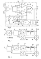
- Fig. 1 denotes a single sideband modulator, 2 a first input for a modulating LF signal or an input signal N (t), which is dependent on the time t, and 4 an adder, to which a residual carrier signal R 1 is supplied.
- the adder 4 is connected to the input of a phase isolator or Hilbert transformer 5, which splits an input signal into several component signals that have a fixed phase relationship to one another.
- n (t) is the peak value
- ⁇ (t) the phase angle of x (t).
- Hilbert transformers are known from: Electronic Design 19, Sept. 13, 1976, pp. 90-94 and from AEÜ (Archive for Electronics and Transmission Technology) 36 (1982) H. 7/8, pp. 304-310.
- the component signal x is fed to an adder input of an adder 6 and the component signal y is fed to an adder input of a further adder 7.
- a second carrier input of the adder 6 is supplied with a residual carrier signal R 2 and a second carrier input of the adder 7 with a residual carrier signal R 3 .
- the residual carrier signals R 1 , R 2 , R 3 are constant. If the residual carrier signal R by means of the adder 4 to the NF-Eingangssighal N (t) is supplied, then the adders are unnecessary 6 and 7. On the other hand it is sufficient if a residual carrier signal R 2 x only a component signal, for example, is added by means of the adder 6 ; then the adders 4 and possibly also 7 can be omitted.
- the input signals X (t) and Y (t) are squared, the squares are added and the root is taken from the sum of the squares, so that a modulator amplitude signal is present at an output 9 of the amplitude calculator 8 and at the same time at an output of the single sideband modulator 1 is available that has no phase component.
- the sum signal X is also connected on the one hand directly to a switch contact 13 of a cyclic switch 16 and on the other hand via an inverter 10 to a switch contact 15 of the cyclic switch 16, which is offset by 180 ° with respect to the switch contact 13.
- the sum signal Y is also connected, on the one hand, directly to a switch contact 12 of the cyclic switch 16 and, on the other hand, via an inverter 11 to a switch contact 14 of the cyclic switch 16, which is offset by 180 ° with respect to the switch contact 12, the switch contact 12 relative to the switch contact 13 is offset by 90 °.
- the switching connection of the switching contact 13, indicated by an arrow P, with an output 16 'of the cyclic switch 16 rotates clockwise when the lower side band is used, ie the output 16' is connected in succession to the switching contacts 12, 15, 14, 13, 12 etc. connected.
- the switching connection rotates counterclockwise one after the other via the switching contacts 14, 15, 12 etc.
- the rotation frequency is equal to a clock frequency f T of 100 kHz, corresponding to 4 times the angular frequency of the carrier signal with a carrier frequency f 1 of 25 kHz.
- the cyclic switch 16 is an electronic switch without rotating parts.
- the scanning signal at the output of the cyclic switch 16 is fed to a quotient or divider 17 as a dividend, and the modulator amplitude signal Z (t) from the output of the amplitude calculator 8 as a divisor.
- the output signal of the divider 7, which is time-discretely provided by the cyclic switch 16, is fed to a bandpass filter 18, on the output side of which a continuous modulator phase signal 19 is available, undesired secondary oscillations being filtered out by the bandpass filter 18.
- the single-sideband modulator forms a current high-frequency phase signal and a current amplitude value from a low-frequency signal, such that the product of these two signals results in a single-sideband-modulated signal.
- the product formation is carried out in the high-frequency output stage, whereby all methods known from amplitude modulation can be used (anode modulation, grid modulation, cathode base circuit, grid base circuit).
- the modulator can be built using analog or digital technology. Mixed solutions with simultaneous use of analog and digital technology are also possible.
- the LF signal N is fed to the analog-digital converter 20 via the input 2, and on the output side it is connected to the input of a digitally constructed single-sideband modulator 1, corresponding to FIG. 1, to which the input signal is fed digitally.
- a new pair of values is available every 10 ps at the outputs of the Hilbert transformer 5. Since all calculations must be carried out with a precision of 12 bits within a sampling period of 10 ps, signal processors are used as digital components.
- the single-sideband modulator 1 is designed using analog circuit technology.
- the input signal N and also the output signals of the single sideband modulator 1 are analog voltages.
- the digitalization for the digital-to-analog converter 21, which is designed as a switching amplifier with pulse-stage modulation, takes place behind the single-sideband modulator 1 by means of an analog-to-digital converter 20.
- the modulator amplitude signal Z can instead of the anode 23 of the RF output tube also on another grid, e.g. be put on the screen grid, the tube.
- the modulator phase signal 19 can also be in control connection with the cathode of the RF output stage tube 26 instead of with the control grid.
- the bandpass filter can also be integrated in the frequency converter 25 instead of in the single sideband modulator 1.
- the divider 17 may be missing in the single sideband modulator 1, the sampling signal used for the phase modulation having an amplitude component.
Landscapes
- Amplitude Modulation (AREA)
- Transmitters (AREA)
Abstract
Um einen Einseitenbandsender hoher Leistung mit nur einer Senderöhre betreiben zu können, wird ein Einseitenbandmodulator (1) verwendet, der in Abhängigkeit von einem modulierenden NF-Signal (2) ein phasenfreies Modulator-Amplitudensignal (9) erzeugt, das über einen als Schaltverstärker mit Puls-Stufenmodulation ausgeführten Digital-Analog-Wandler (21) und ein HF-Filter (22) die Anode (23) einer HF-Endstufenröhre (26) in der Amplitude moduliert. Der Einseitenbandmodulator (1) liefert ferner ein vorzugsweise nicht amplitudenabhängiges Modulator-Phasensignal (19), das dem Steuergitter der HF-Endstufenröhre (26) gegebenenfalls über einen Frequenzumsetzer (25) zugeführt ist. Der Einseitenbandmodulator (1) kann digital oder analog aufgebaut sein; er weist eingangsseitig einen Hilberttransformator (5) auf, der das modulierende Eingangssignal (2) in zwei um 90° phasenverschobene Komponentensignale aufspaltet, er weist ferner ausgangsseitig einen Amplitudenrechner (8), einen zyklischen Schalter (16) mit einer Taktfrequenz (fT), die vorzugsweise gleich der 4fachen Trägerfrequenz (f1) ist, und gegebenenfalls einen Quotientenrechner (17) mit daran anschließendem Bandpaßfilter (18) auf. Dem Eingangssignal (2) oder den Ausgangssignalen des Hilberttransformators (5) kann ein Restträgersignal (R1, R2, R3) beigefügt werden.In order to be able to operate a high-power single-sideband transmitter with only one transmitter tube, a single-sideband modulator (1) is used which, depending on a modulating LF signal (2), generates a phase-free modulator amplitude signal (9), which is used as a switching amplifier with a pulse -Stage modulation digital-analog converter (21) and an RF filter (22) modulates the anode (23) of an RF power amplifier tube (26) in amplitude. The single-sideband modulator (1) also supplies a preferably non-amplitude-dependent modulator phase signal (19) which is fed to the control grid of the RF output stage tube (26) via a frequency converter (25) if necessary. The single sideband modulator (1) can be constructed digitally or analogously; it has a Hilbert transformer (5) on the input side, which splits the modulating input signal (2) into two component signals that are phase-shifted by 90 °; is preferably equal to 4 times the carrier frequency (f1), and optionally a quotient computer (17) with a bandpass filter (18) connected to it. A residual carrier signal (R1, R2, R3) can be added to the input signal (2) or the output signals of the Hilbert transformer (5).
Description
Bei der Erfindung wird ausgegangen von einem Einseitenbandmodulationsverfahren nach dem Oberbegriff des Patentanspruchs 1. Die Erfindung betrifft auch einen Einseitenbandmodulator und einen Rundfunksender mit einem Einseitenbandmodulator.The invention is based on a single sideband modulation method according to the preamble of
Mit dem Oberbegriff nimmt die Erfindung auf einen Stand der Technik Bezug, wie er in dem deutschen Buch: H.Meinke und F.W.Gundlach, Taschenbuch der Hochfrequenztechnik, Springer-Verlag Berlin/Heidelberg/New York 1968, S. 1323-1325, beschrieben ist. Dort ist ein Einseitenbandmodulator für grossen Frequenzbereich der Trägerschwingung und breites Niederfrequenzband, nach Lenehan, dargestellt und beschrieben, bei dem für beide Frequenzbereiche Phasenteiler vorgesehen sind, die um 90° phasenverschobene Komponentensignale erzeugen. Diese Komponentensignale speisen zwei Ringmodulatoren, welche ihrerseits drei Endverstärkerröhren ansteuern. Nachteilig dabei ist, dass drei Röhren benötigt werden, die in ihrem linearen Bereich, d.h. in A- oder B-Betrieb betrieben werden müssen.With the generic term, the invention refers to a state of the art, as described in the German book: H.Meinke and FWGundlach, Taschenbuch der Hochfrequenztechnik, Springer-Verlag Berlin / Heidelberg / New York 1968, pp. 1323-1325. There, a single-sideband modulator for a large frequency range of the carrier oscillation and a broad low-frequency band, according to Lenehan, is shown and described, in which phase dividers are provided for both frequency ranges, which generate component signals that are phase-shifted by 90 °. These component signals feed two ring modulators, which in turn three Activate power amplifier tubes. The disadvantage here is that three tubes are required which have to be operated in their linear range, ie in A or B mode.
Die Erfindung, wie sie in den Patentansprüchen 1, 6, 10 und 11 definiert ist, löst die Aufgabe, ein Einseitenbandmodulationsverfahren, einen Einseitenbandmodulator und einen Rundfunksender mit Einseitenbandmodulation anzugeben, mit denen es möglich ist, einen Einseitenbandsender hoher Leistung mit nur einer Senderöhre zu betreiben.The invention, as defined in
Ein Vorteil der Erfindung liegt darin, dass die Senderöhre nicht in ihrem linearen Bereich betrieben werden muss, sondern bei beliebiger Aussteuerung im C-Betrieb mit einem höheren Anodenwirkungsgrad betrieben werden kann. Ein weiterer Vorteil besteht darin, dass sich Rundfunksender mit Amplitudenmodulation bei Bedarf unter Verwendung des erfindungsgemässen Einseitenbandmodulators leicht nachrüsten und auf Einseitenbandtechnik umstellen lassen.An advantage of the invention is that the transmitter tube does not have to be operated in its linear range, but can be operated with a higher anode efficiency in C mode with any modulation. Another advantage is that radio transmitters with amplitude modulation can be easily retrofitted using the single-sideband modulator according to the invention and converted to single-sideband technology.
Unter Verwendung eines Modulations-Schaltverstärkers mit Puls-Stufenmodulation kann bei einem Rundfunksender ein hoher Modulatorwirkungsgrad und auch ein verbesserter Gesamtwirkungsgrad bei Einseitenbandmodulation erreicht werden. Da der Modulations-Schaltverstärker weitaus geringere Verlust aufweist als eine vergleichbare Modulationsröhre, resultiert ein hoher Gesamtwirkungsgrad des Senders. Der erhöhte Schaltungsaufwand für den Modulations-Schaltverstärker wird durch den geringeren Stromverbrauch rasch amortisiert. Der Modulations-Schaltverstärker hat einen geringen Platzbedarf und niedrige Betriebskosten, da keine Röhrenersatzkosten anfallen.Using a modulation switching amplifier with pulse stage modulation, a radio transmitter can achieve a high modulator efficiency and also an improved overall efficiency with single-sideband modulation. Since the modulation switching amplifier has a much lower loss than a comparable modulation tube, the transmitter's overall efficiency is high. The increased circuitry for the modulation switching amplifier is quickly amortized by the lower power consumption. The modulation switching amplifier has a small footprint and low operating costs because there are no tube replacement costs.
Bei einem Rundfunksender gewährleistet die geringe Zahl von Leistungskomponenten und Verschleissteilen neben einem hohen Wirkungsgrad eine hohe Verfügbarkeit, geringe Wartungskosten und ausgezeichnete Wartungsfreundlichkeit.In the case of a radio transmitter, the low number of power components and wearing parts ensures, in addition to high efficiency, high availability, low maintenance costs and excellent maintenance friendliness.
Gemäss einer vorteilhaften Ausgestaltung der Erfindung ist es möglich, das Einseitenbandsignal auch zusammen mit einem Trägersignal auszusenden.According to an advantageous embodiment of the invention, it is also possible to transmit the single sideband signal together with a carrier signal.
Zum einschlägigen Stand der Technik wird zusätzlich auf die Schweizer Firmenzeitschrift Brown Boveri Mitteilungen 5, 1984, S. 202 - 205 verwiesen, aus der es für einen 600-kW-Mittelwellensender bekannt ist, mit nur einer HF-(Hochfrequenz-)Hochleistungstetrode in der Endstufe und mit einem volltransistorisierten Modulations-Schaltverstärker mit Puls-Stufenmodulation bei Zweiseitenbandtechnik einen hohen Modulatorwirkungsgrad und auch einen hohen Gesamtwirkungsgrad des Senders zu erreichen. Dort wird das für die Amplitudenmodulation notwendige Produkt aus NF-(Niederfrequenz-)Signal und Hochfrequenzträger direkt in der HF-Endstufe gebildet. Dabei wird der Hochfrequenzträger mit konstanter Amplitude auf das Gitter der HF-Endstufe gegben. Das aufzumodulierende NF-Signal steuert einen sogenannten Pulser, d.h. den Modulations-Schaltverstärker mit Pulsstufenmodulation bzw. einen der Sendeleistung entsprechend grossen Digital-Analog-Wandler, der die Anodenspannung entpsrechend der momentanen Sendeleistung erzeugt.For the relevant state of the art, reference is also made to the Swiss company magazine Brown Boveri Mitteilungen 5, 1984, pp. 202-205, from which it is known for a 600 kW medium-wave transmitter, with only one HF (high-frequency) high-performance tetrode in the To achieve a high modulator efficiency and also a high overall efficiency of the transmitter with a fully transistorized modulation switching amplifier with pulse stage modulation with double sideband technology. There, the product of LF (low-frequency) signal and high-frequency carrier necessary for the amplitude modulation is formed directly in the HF output stage. The high-frequency carrier is placed on the grid of the RF output stage with a constant amplitude. The LF signal to be modulated controls a so-called pulser, i.e. the modulation switching amplifier with pulse stage modulation or a digital-analog converter which is large in accordance with the transmission power and which generates the anode voltage in accordance with the current transmission power.
Die Erfindung wird nachstehend anhand von Ausführungsbeispielen erläutert. Es zeigen:
- Fig. 1 einen Einseitenbandmodulator,
- Fig. 2 ein vereinfachtes Prinzipschema eines Rundfunksenders mit einem Einseitenbandmodulator gemäss Fig. I in digitaler Version und
- Fig. 3 ein vereinfachtes Prinzipschema eines Rundfunksenders mit einem Einseitenbandmodulators gemäss Fig. 1 in analoger Version.
- 1 shows a single sideband modulator,
- Fig. 2 is a simplified schematic diagram of a radio transmitter with a single sideband modulator according to Fig. I in digital version and
- Fig. 3 is a simplified schematic diagram of a radio transmitter with a single sideband modulator according to Fig. 1 in an analog version.
In Fig. 1 bezeichnet 1 einen Einseitenbandmodulator, 2 einen ersten Eingang für ein modulierendes NF-Signal bzw. ein Eingangssignal N(t), das von der Zeit t abhängig ist, und 4 ein Addierglied, dem über einen zweiten Eingang 3 ein Restträgersignal R1 zugeführt ist.In Fig. 1, 1 denotes a single sideband modulator, 2 a first input for a modulating LF signal or an input signal N (t), which is dependent on the time t, and 4 an adder, to which a residual carrier signal R 1 is supplied.
Ausgangsseitig ist das Addierglied 4 mit dem Eingang eines Phasentrenners bzw. Hilberttransformators 5 verbunden, der ein Eingangssignal in mehrere Komponentensignale aufspaltet, die eine feste Phasenbeziehung zueinander haben. Im dargestellten Beispiel wird das Eingangssignal N der Uebersichtlichkeit halber ohne Restträgersignal R1 in zwei um 90° phasenverschobene Komponentensignale x(t) = n(t) - sin ϕ(t) und y(t) = n(t) · cos ϕ(t) aufgespaltet, deren Summe dem ursprünglichen Signal N(t) entspricht. Dabei ist n(t) der Scheitelwert und ϕ(t) der Phasenwinkel von x(t). Hilberttransformatoren sind bekannt aus: Electronic Design 19, Sept. 13, 1976, S. 90 - 94 und aus AEÜ (Archiv für Elektronik und Uebertragungstechnik) 36 (1982) H. 7/8, S. 304-310.On the output side, the
Das Komponentensignal x ist einem Addiereingang eines Addiergliedes 6 und das Komponentensignal y einem Addiereingang eines weiteren Addiergliedes 7 zugeführt. Einem zweiten Addiereingang des Addiergliedes 6 ist ein Restträgersignal R2 und einem zweiten Addiereingang des Addiergliedes 7 ein Restträgersignal R3 zugeführt.The component signal x is fed to an adder input of an
Die Restträgersignale R1, R2, R3 sind konstant. Wenn das Restträgersignal R mittels des Addiergliedes 4 dem NF-Eingangssighal N(t) zugeführt wird, dann erübrigen sich die Addierglieder 6 und 7. Andererseits genügt es, wenn ein Restträgersignal R2 nur einem Komponentensignal, z.B. x, mittels des Addiergliedes 6 zugefügt wird; dann können die Addierglieder 4 und gegebenenfalls auch 7 entfallen.The residual carrier signals R 1 , R 2 , R 3 are constant. If the residual carrier signal R by means of the
Das Addierglied 6 liefert eingangsseitig ein Summensignal X(t) = x(t) + R2, das einem ersten Eingang eines Amplitudenrechners 8 zugeführt ist. Das Addierglied 7 liefert ausgangsseitig ein Summensignal Y(t) = y(t) + R3, das einem dritten Eingang des Amplitudenrechners 8 zugeführt ist. Im Amplitudenrechner 8 werden die Eingangssignale X(t) und Y(t) quadriert, die Quadrate addiert und aus der Quadratsumme die Wurzel gezogen, so dass an einem Ausgang 9 des Amplitudenrechners 8 und gleichzeitig an einem Ausgang des Einseitenbandmodulators 1 ein Modulator-Amplitudensignal ![]()
![]()
Das Summensignal X ist ferner einerseits direkt mit einem Schaltkontakt 13 eines zyklischen Schalters 16 und andererseits über einen Inverter 10 mit einem Schaltkontakt 15 des zyklischen Schalters 16 verbunden, der bezüglich des Schaltkontaktes 13 um 180° versetzt ist.The sum signal X is also connected on the one hand directly to a
Das Summensignal Y ist ferner einerseits direkt mit einem Schaltkontakt 12 des zyklischen Schalters 16 und andererseits über einen Inverter 11 mit einem Schaltkontakt 14 des zyklischen Schalters 16 verbunden, der bezüglich des Schaltkontaktes 12 um 180° versetzt ist, wobei der Schaltkontakt 12 gegenüber dem Schaltkontakt 13 um 90° versetzt ist.The sum signal Y is also connected, on the one hand, directly to a switch contact 12 of the
Die durch einen Pfeil P angedeutete Schaltverbindung des Schaltkontaktes 13 mit einem Ausgang 16' des zyklischen Schalters 16 rotiert bei Verwendung des unteren Seitenbandes im Uhrzeigersinn, d.h., der Ausgang 16' wird nacheinander mit den Schaltkontakten 12, 15, 14, 13, 12 usw. verbunden. Bei Verwendung des oberen Seitenbandes rotiert die Schaltverbindung entgegen dem Uhrzeigersinn nacheinander über die Schaltkontakte 14, 15, 12 usw. Die Rotationsfrequenz ist gleich einer Taktfrequenz fT von 100 kHz, entsprechend der 4fachen Kreisfrequenz des Trägersignals mit einer Trägerfrequenz f1 von 25 kHz. Der zyklische Schalter 16 ist ein elektronischer Schalter ohne rotierende Teile. Mit dieser Rotationsfrequenz erhält man am Ausgang 16', unter Voraussetzung, dass kein Restträgersignal R1 oder R2 oder R3 zugefügt wurde, ein Abtastsignal n(ti) · cos (ωti + ϕ(ti), wobei das "+"-Zeichen für das obere und das "-"-Zeichen für das untere Seitenband gilt.The switching connection of the
Unter der Annahme: R1 = 0, R2 ≠ 0, R3 = 0 gilt für das obere Seitenband und die Schaltkontakte 12 ... 14:
- 12: n(t1) · cos ϕ(t1) + 0 = n(t1) · cos ϕ(t1) + R2 · sin(ωt1),
- 13: n(t2) · sin ϕ(t2) + R2 = n(t2) · sin ϕ(t2) + R2 · sin(ωt2),
- 14: -n(t3) · cos ϕ(t3) + 0 = -n(t3) · cos ϕ(t3) + R2 · sin(ωt3),
- 15: -n(t4) · sin ϕ(t4) - R2 = -n(t4) · sin ϕ(t4) + R2 · sin(ωt4) = n(ti) · cos(ωti+ϕ(ti)) + R2 · sin(ωti).
- 12: n (t 1 ) cos ϕ (t 1 ) + 0 = n (t 1 ) cos ϕ (t 1 ) + R 2 sin (ωt 1 ),
- 13: n (t 2 ) sin ϕ (t 2 ) + R 2 = n (t 2 ) sin ϕ (t 2 ) + R 2 sin (ωt 2 ),
- 14: -n (t 3 ) cos ϕ (t 3 ) + 0 = -n (t 3 ) cos ϕ (t 3 ) + R 2 sin (ωt 3 ),
- 15: -n (t 4 ) sin ϕ (t 4 ) - R 2 = -n (t 4 ) sin ϕ (t 4 ) + R 2 sin (ωt 4 ) = n (t i ) cos ( ωt i + ϕ (t i )) + R 2 · sin (ωt i ).
Die obigen Gleichungen sind leicht ersichtlich, wenn man für ωti nacheinander die Wert 0, Π/2, Π und 3Π/2 einsetzt.The above equations are easy to see if the values 0, Π / 2, Π and 3Π / 2 are used in succession for ωt i .
Das Abtastsignal am Ausgang des zyklischen Schalters 16 wird einem Quotientenbildner bzw. Dividierer 17 als Dividend zugeführt, und das Modulator-Amplitudensignal Z(t) vom Ausgang des Amplitudenrechners 8 als Divisor. Am Ausgang des Dividierers 7 erhält man ein Quotientensignal, das nur phasen- und nicht amplitudenabhängig = cos(ωti + ϕ(ti)) ist.The scanning signal at the output of the
Das durch den zyklischen Schalter 16 zeitdiskret vorhandene Ausgangssignal des Dividierers 7 wird einem Bandpassfilter 18 zugeführt, an dem ausgangsseitig ein kontinuierliches Modulator-Phasensignal 19 zur Verfügung steht, wobei unerwünschte Nebenschwingungen durch das Bandpassfilter 18 ausgefiltert werden. Das Bandpassfilter 18 ist für 75 kHz ausgelegt, d.h. bezüglich 50 kHz (= Nyquistfrequenz zur Trägersignalfrequenz von 25 kHz) gespiegelt.The output signal of the
Wichtig ist, dass der Einseitenbandmodulator aus einem Niederfrequenzsignal ein momentanes Hochfrequenzphasensignal und einen momentanen Amplitudenwert bildet, derart, dass das Produkt dieser beiden Signale ein einseitenbandmoduliertes Signal ergibt. Die Produktbildung wird in der Hochfrequenz-Endstufe vorgenommen, wobei alle aus der Amplitudenmodulation bekannten Verfahren anwendbar sind (Anodenmodulation, Gittermodulation, Kathodenbasisschaltung, Gitterbasisschaltung). Der Modulator kann in analoger oder digitaler Technik aufgebaut werden. Auch Mischlösungen mit gleichzeitigem Einsatz analoger und digitaler Technik sind möglich.It is important that the single-sideband modulator forms a current high-frequency phase signal and a current amplitude value from a low-frequency signal, such that the product of these two signals results in a single-sideband-modulated signal. The product formation is carried out in the high-frequency output stage, whereby all methods known from amplitude modulation can be used (anode modulation, grid modulation, cathode base circuit, grid base circuit). The modulator can be built using analog or digital technology. Mixed solutions with simultaneous use of analog and digital technology are also possible.
Fig. 2 zeigt eine Verwendung des Einseitenbandmodulators in einem Hochleistungs-Rundfunksender, wobei aus übersichtlichkeitsgründen nur die für den Anschluss des Einseitenbandmodulators wesentlichen Teile dargestellt sind.2 shows a use of the single sideband modulator in a high-performance radio transmitter, only the parts essential for the connection of the single sideband modulator being shown for reasons of clarity.
Mit 20 ist ein Analog-Digital-Wandler bezeichnet, der mit der Taktfrequenz fT von 100 kHz getaktet ist. Ueber den Eingang 2 ist dem Analog-Digital-Wandler 20 das NF-Signal N zugeführt, ausgangsseitig ist er mit dem Eingang eines digital aufgebauten Einseitenbandmodulators 1, entsprechend Fig. 1, verbunden, dem das Eingangssignal digital zugeführt wird. An den Ausgängen des Hilberttransformators 5 steht alle 10 ps ein neues Wertepaar zur Verfügung. Da sämtliche Berechnungen innerhalb einer Abtastperiode von 10 ps mit einer Genauigkeit von 12 Bit durchgeführt werden müssen, sind als digitale Bausteine Signalprozessoren verwendet.20 denotes an analog-digital converter, which is clocked at the clock frequency f T of 100 kHz. The LF signal N is fed to the analog-
Bei der Ausführung eines Hochleistungs-Rundfunksenders gemäss Fig. 3 ist der Einseitenbandmodulator 1 in analoger Schaltungstechnik ausgeführt. Das Eingangssignal N und auch die Ausgangssignale des Einseitenbandmodulators 1 sind analoge Spannungen. Die Digitalisierung für den als Schaltverstärker mit Puls-Stufenmodulation ausgeführten Digital-Analog-Wandler 21 erfolgt hinter dem Einseitenbandmodulator 1 mittels eines Analog-DigitalWandlers 20.3, the single-
Das Modulator-Amplitudensignal Z kann statt auf die Anode 23 der HF-Endstufenröhre auch auf ein weiteres Gitter, z.B. auf das Schirmgitter, der Röhre gegeben werden. Das Modulator-Phasensignal 19 kann anstelle mit dem Steuergitter der HF-Endstufenröhre 26 auch mit deren Kathode in Steuerverbindung stehen. Das Bandpassfilter kann anstelle im Einseitenbandmodulator 1 auch in den Frequenzumsetzer 25 integriert sein. Schliesslich kann der Dividierer 17 im Einseitenbandmodulator 1 fehlen, wobei das für die Phasenmodulation verwendete Abtastsignal einen Amplitudenanteil aufweist.The modulator amplitude signal Z can instead of the
Claims (11)
dadurch gekennzeichnet,
characterized,
dadurch gekennzeichnet,
characterized,
Applications Claiming Priority (2)
| Application Number | Priority Date | Filing Date | Title |
|---|---|---|---|
| CH671/85A CH667762A5 (en) | 1985-02-14 | 1985-02-14 | SINGLE SIDE BAND MODULATION METHOD, SINGLE SIDE BAND MODULATOR AND BROADCASTING TRANSMITTER. |
| CH671/85 | 1985-02-14 |
Publications (2)
| Publication Number | Publication Date |
|---|---|
| EP0193655A1 true EP0193655A1 (en) | 1986-09-10 |
| EP0193655B1 EP0193655B1 (en) | 1989-08-16 |
Family
ID=4192443
Family Applications (1)
| Application Number | Title | Priority Date | Filing Date |
|---|---|---|---|
| EP85116487A Expired EP0193655B1 (en) | 1985-02-14 | 1985-12-23 | Single sideband modulation process, single sideband modulator and radio-transmitter |
Country Status (16)
| Country | Link |
|---|---|
| US (1) | US4656440A (en) |
| EP (1) | EP0193655B1 (en) |
| JP (1) | JPS61192102A (en) |
| CN (1) | CN86100908B (en) |
| BG (1) | BG43699A3 (en) |
| BR (1) | BR8600415A (en) |
| CA (1) | CA1244895A (en) |
| CH (1) | CH667762A5 (en) |
| CS (1) | CS269977B2 (en) |
| DE (1) | DE3572427D1 (en) |
| ES (1) | ES8801482A1 (en) |
| IN (1) | IN167082B (en) |
| PL (2) | PL154067B1 (en) |
| SU (1) | SU1570660A3 (en) |
| YU (2) | YU17386A (en) |
| ZA (1) | ZA86917B (en) |
Cited By (5)
| Publication number | Priority date | Publication date | Assignee | Title |
|---|---|---|---|---|
| EP0360990A1 (en) * | 1988-09-15 | 1990-04-04 | Thomcast Ag | Method for generating an amplitude-modulated ISB signal, and device for carrying out the method |
| US5166631A (en) * | 1990-12-08 | 1992-11-24 | Asea Brown Boveri Ltd. | Circuit for regeneration and bandwidth limitation of a quasi-periodic digital signal |
| EP0708546A2 (en) * | 1994-10-21 | 1996-04-24 | Deutsche Telekom AG | QAM communication method |
| EP0708545A2 (en) * | 1994-10-21 | 1996-04-24 | Deutsche Telekom AG | Narrowband QAM transmission |
| DE10117563B4 (en) * | 2001-04-07 | 2006-04-13 | Interessengemeinschaft für Rundfunkschutzrechte GmbH Schutzrechtsverwertung & Co. KG. | Method for amplifying an amplitude and / or phase modulated high frequency signal according to the principle of Envelope Elimination and Restoration and circuitry |
Families Citing this family (5)
| Publication number | Priority date | Publication date | Assignee | Title |
|---|---|---|---|---|
| US4973977A (en) * | 1988-11-29 | 1990-11-27 | Comlux | Digital to amplitude modulated analog converter |
| DE4210069A1 (en) * | 1992-03-27 | 1993-09-30 | Asea Brown Boveri | Amplitude-modulated radio transmitter for various types of modulation, especially DSB, SSB and ISB |
| FR2788390B1 (en) * | 1999-01-12 | 2003-05-30 | Thomson Csf | HIGH EFFICIENCY SHORTWAVE BROADCAST TRANSMITTER OPTIMIZED FOR DIGITAL TYPE TRANSMISSIONS |
| US7319763B2 (en) * | 2001-07-11 | 2008-01-15 | American Technology Corporation | Power amplification for parametric loudspeakers |
| US9106414B2 (en) * | 2009-09-09 | 2015-08-11 | Edward W. Laves | Method and apparatus for wirelessly transmitting high volume content to an electronic device |
Citations (2)
| Publication number | Priority date | Publication date | Assignee | Title |
|---|---|---|---|---|
| US2988711A (en) * | 1959-03-20 | 1961-06-13 | Packard Bell Electronics | Single sideband generator |
| EP0112410A1 (en) * | 1982-12-28 | 1984-07-04 | BBC Brown Boveri AG | Single side-band transmitter |
Family Cites Families (1)
| Publication number | Priority date | Publication date | Assignee | Title |
|---|---|---|---|---|
| DE3040272C2 (en) * | 1980-10-23 | 1983-02-03 | Licentia Patent-Verwaltungs-Gmbh, 6000 Frankfurt | Amplitude-modulated transmitter for single sideband operation |
-
1985
- 1985-02-14 CH CH671/85A patent/CH667762A5/en not_active IP Right Cessation
- 1985-12-23 EP EP85116487A patent/EP0193655B1/en not_active Expired
- 1985-12-23 DE DE8585116487T patent/DE3572427D1/en not_active Expired
-
1986
- 1986-01-03 CS CS8677A patent/CS269977B2/en unknown
- 1986-01-23 JP JP61012976A patent/JPS61192102A/en active Pending
- 1986-01-24 CA CA000500360A patent/CA1244895A/en not_active Expired
- 1986-01-27 IN IN48/MAS/86A patent/IN167082B/en unknown
- 1986-01-30 US US06/824,091 patent/US4656440A/en not_active Expired - Lifetime
- 1986-02-03 BR BR8600415A patent/BR8600415A/en not_active IP Right Cessation
- 1986-02-06 YU YU00173/86A patent/YU17386A/en unknown
- 1986-02-07 ZA ZA86917A patent/ZA86917B/en unknown
- 1986-02-10 SU SU864020351A patent/SU1570660A3/en active
- 1986-02-11 BG BG8673488A patent/BG43699A3/en unknown
- 1986-02-12 PL PL1986285439A patent/PL154067B1/en unknown
- 1986-02-12 PL PL1986257920A patent/PL152367B1/en unknown
- 1986-02-14 CN CN86100908A patent/CN86100908B/en not_active Expired
- 1986-02-14 ES ES552053A patent/ES8801482A1/en not_active Expired
-
1989
- 1989-06-21 YU YU01270/89A patent/YU127089A/en unknown
Patent Citations (2)
| Publication number | Priority date | Publication date | Assignee | Title |
|---|---|---|---|---|
| US2988711A (en) * | 1959-03-20 | 1961-06-13 | Packard Bell Electronics | Single sideband generator |
| EP0112410A1 (en) * | 1982-12-28 | 1984-07-04 | BBC Brown Boveri AG | Single side-band transmitter |
Non-Patent Citations (2)
| Title |
|---|
| BROWN, BOVERI REVIEW, Band 72, Nr. 7, Juli 1985, Seiten 332-335, Baden, CH; M. GAUTSCHI et al.: "A new method of single-sideband modulation for high-power broadcasting transmitters" * |
| GEC JOURNAL OF SCIENCE & TECHNOLOGY, Band 39, Nr. 2, 1972, Seiten 61-69, Wenbley, Middlesex, GB; W. SARAGA: "Frequency-selective networks suitable for microelectronic realization-2" * |
Cited By (9)
| Publication number | Priority date | Publication date | Assignee | Title |
|---|---|---|---|---|
| EP0360990A1 (en) * | 1988-09-15 | 1990-04-04 | Thomcast Ag | Method for generating an amplitude-modulated ISB signal, and device for carrying out the method |
| US4955072A (en) * | 1988-09-15 | 1990-09-04 | Asea Brown Boveri Ltd | Method of generating an amplitude-modulated ISB transmission signal and apparatus for carrying out the method |
| CH675802A5 (en) * | 1988-09-15 | 1990-10-31 | Asea Brown Boveri | |
| US5166631A (en) * | 1990-12-08 | 1992-11-24 | Asea Brown Boveri Ltd. | Circuit for regeneration and bandwidth limitation of a quasi-periodic digital signal |
| EP0708546A2 (en) * | 1994-10-21 | 1996-04-24 | Deutsche Telekom AG | QAM communication method |
| EP0708545A2 (en) * | 1994-10-21 | 1996-04-24 | Deutsche Telekom AG | Narrowband QAM transmission |
| EP0708545A3 (en) * | 1994-10-21 | 1998-09-23 | Deutsche Telekom AG | Narrowband QAM transmission |
| EP0708546A3 (en) * | 1994-10-21 | 1998-09-30 | Deutsche Telekom AG | QAM communication method |
| DE10117563B4 (en) * | 2001-04-07 | 2006-04-13 | Interessengemeinschaft für Rundfunkschutzrechte GmbH Schutzrechtsverwertung & Co. KG. | Method for amplifying an amplitude and / or phase modulated high frequency signal according to the principle of Envelope Elimination and Restoration and circuitry |
Also Published As
| Publication number | Publication date |
|---|---|
| PL257920A1 (en) | 1986-10-21 |
| SU1570660A3 (en) | 1990-06-07 |
| CS7786A2 (en) | 1989-09-12 |
| PL152367B1 (en) | 1990-12-31 |
| CA1244895A (en) | 1988-11-15 |
| ZA86917B (en) | 1986-09-24 |
| IN167082B (en) | 1990-08-25 |
| BG43699A3 (en) | 1988-07-15 |
| CH667762A5 (en) | 1988-10-31 |
| JPS61192102A (en) | 1986-08-26 |
| BR8600415A (en) | 1986-10-14 |
| CN86100908B (en) | 1988-06-22 |
| US4656440A (en) | 1987-04-07 |
| ES552053A0 (en) | 1987-12-16 |
| YU127089A (en) | 1992-05-28 |
| YU17386A (en) | 1990-02-28 |
| CS269977B2 (en) | 1990-05-14 |
| EP0193655B1 (en) | 1989-08-16 |
| PL154067B1 (en) | 1991-06-28 |
| DE3572427D1 (en) | 1989-09-21 |
| ES8801482A1 (en) | 1987-12-16 |
| CN86100908A (en) | 1986-08-20 |
Similar Documents
| Publication | Publication Date | Title |
|---|---|---|
| DE2304352A1 (en) | CIRCUIT ARRANGEMENT FOR AMPLIFYING AN INPUT SIGNAL | |
| EP0344467B1 (en) | Quadrature receiver | |
| EP0360990B1 (en) | Method for generating an amplitude-modulated ISB signal, and device for carrying out the method | |
| EP0193655B1 (en) | Single sideband modulation process, single sideband modulator and radio-transmitter | |
| DE4216065A1 (en) | Microwave signal A=D conversion by Mach-Zehnder modulator-interferometer - offsetting optical carriers by microwave frequency and feeding as electrical signals to comparator, with electric fields in optical waveguides differing by factor of two | |
| US4162455A (en) | Amplifier systems | |
| DE10101911B4 (en) | Signal processing of an amplitude and / or phase modulated radio frequency signal | |
| DE611807C (en) | Arrangement for phase modulating radio transmitters | |
| EP0112410B2 (en) | Single side-band transmitter | |
| EP0708545B1 (en) | Narrowband QAM transmission | |
| DE10117563B4 (en) | Method for amplifying an amplitude and / or phase modulated high frequency signal according to the principle of Envelope Elimination and Restoration and circuitry | |
| US2501355A (en) | Phase modulated transmitter with feedback | |
| US2692371A (en) | Modulator circuit | |
| DE102008049666B4 (en) | Digital modulation | |
| DE839812C (en) | Circuit for transforming the waveform of an alternating voltage | |
| DE2721119A1 (en) | FREQUENCY CONVERTER CIRCUIT | |
| DE624089C (en) | Process for generating electromagnetic oscillations which are either only amplitude or only frequency modulated | |
| EP3411955B1 (en) | Circuit arrangement and method for generating a radio-frequency, analogue transmission signal using reduced interference signals | |
| EP0146195A2 (en) | FM stereo receiver | |
| EP0335284A2 (en) | Phase to digital conversion method and arrangement for carrying out the method | |
| GB760602A (en) | Electrical apparatus for multiplication of two functions | |
| EP3624334A1 (en) | Device for the conversion of an analogous input signal into a digital output signal | |
| DE102010011468B4 (en) | Method and circuit arrangement for transforming an HF signal in the band-pass pulse length modulation | |
| DE1766981C3 (en) | N-path filter | |
| DE2550545C2 (en) | Radio transceiver |
Legal Events
| Date | Code | Title | Description |
|---|---|---|---|
| PUAI | Public reference made under article 153(3) epc to a published international application that has entered the european phase |
Free format text: ORIGINAL CODE: 0009012 |
|
| AK | Designated contracting states |
Kind code of ref document: A1 Designated state(s): CH DE FR GB LI NL |
|
| 17P | Request for examination filed |
Effective date: 19861205 |
|
| RAP1 | Party data changed (applicant data changed or rights of an application transferred) |
Owner name: BBC BROWN BOVERI AG |
|
| 17Q | First examination report despatched |
Effective date: 19881124 |
|
| GRAA | (expected) grant |
Free format text: ORIGINAL CODE: 0009210 |
|
| AK | Designated contracting states |
Kind code of ref document: B1 Designated state(s): CH DE FR GB LI NL |
|
| REF | Corresponds to: |
Ref document number: 3572427 Country of ref document: DE Date of ref document: 19890921 |
|
| GBT | Gb: translation of ep patent filed (gb section 77(6)(a)/1977) | ||
| ET | Fr: translation filed | ||
| PLBE | No opposition filed within time limit |
Free format text: ORIGINAL CODE: 0009261 |
|
| STAA | Information on the status of an ep patent application or granted ep patent |
Free format text: STATUS: NO OPPOSITION FILED WITHIN TIME LIMIT |
|
| 26N | No opposition filed | ||
| PGFP | Annual fee paid to national office [announced via postgrant information from national office to epo] |
Ref country code: NL Payment date: 19911231 Year of fee payment: 7 |
|
| PG25 | Lapsed in a contracting state [announced via postgrant information from national office to epo] |
Ref country code: NL Effective date: 19930701 |
|
| NLV4 | Nl: lapsed or anulled due to non-payment of the annual fee | ||
| REG | Reference to a national code |
Ref country code: GB Ref legal event code: 732E |
|
| REG | Reference to a national code |
Ref country code: FR Ref legal event code: CD |
|
| REG | Reference to a national code |
Ref country code: FR Ref legal event code: CD |
|
| REG | Reference to a national code |
Ref country code: CH Ref legal event code: PUE Owner name: THOMCAST AG |
|
| REG | Reference to a national code |
Ref country code: FR Ref legal event code: TP |
|
| PGFP | Annual fee paid to national office [announced via postgrant information from national office to epo] |
Ref country code: FR Payment date: 19941108 Year of fee payment: 10 |
|
| PGFP | Annual fee paid to national office [announced via postgrant information from national office to epo] |
Ref country code: GB Payment date: 19941116 Year of fee payment: 10 |
|
| PGFP | Annual fee paid to national office [announced via postgrant information from national office to epo] |
Ref country code: DE Payment date: 19941122 Year of fee payment: 10 |
|
| PGFP | Annual fee paid to national office [announced via postgrant information from national office to epo] |
Ref country code: CH Payment date: 19941222 Year of fee payment: 10 |
|
| PG25 | Lapsed in a contracting state [announced via postgrant information from national office to epo] |
Ref country code: GB Effective date: 19951223 |
|
| PG25 | Lapsed in a contracting state [announced via postgrant information from national office to epo] |
Ref country code: LI Effective date: 19951231 Ref country code: CH Effective date: 19951231 |
|
| GBPC | Gb: european patent ceased through non-payment of renewal fee |
Effective date: 19951223 |
|
| REG | Reference to a national code |
Ref country code: CH Ref legal event code: PL |
|
| PG25 | Lapsed in a contracting state [announced via postgrant information from national office to epo] |
Ref country code: FR Effective date: 19960830 |
|
| PG25 | Lapsed in a contracting state [announced via postgrant information from national office to epo] |
Ref country code: DE Effective date: 19960903 |
|
| REG | Reference to a national code |
Ref country code: FR Ref legal event code: ST |