EP0228242A2 - Non-intrusive microprocessor performance analyzer - Google Patents
Non-intrusive microprocessor performance analyzer Download PDFInfo
- Publication number
- EP0228242A2 EP0228242A2 EP86309830A EP86309830A EP0228242A2 EP 0228242 A2 EP0228242 A2 EP 0228242A2 EP 86309830 A EP86309830 A EP 86309830A EP 86309830 A EP86309830 A EP 86309830A EP 0228242 A2 EP0228242 A2 EP 0228242A2
- Authority
- EP
- European Patent Office
- Prior art keywords
- information
- address
- recited
- read
- port
- Prior art date
- Legal status (The legal status is an assumption and is not a legal conclusion. Google has not performed a legal analysis and makes no representation as to the accuracy of the status listed.)
- Withdrawn
Links
Images


Classifications
-
- G—PHYSICS
- G06—COMPUTING; CALCULATING OR COUNTING
- G06F—ELECTRIC DIGITAL DATA PROCESSING
- G06F11/00—Error detection; Error correction; Monitoring
- G06F11/30—Monitoring
- G06F11/34—Recording or statistical evaluation of computer activity, e.g. of down time, of input/output operation ; Recording or statistical evaluation of user activity, e.g. usability assessment
- G06F11/3466—Performance evaluation by tracing or monitoring
- G06F11/348—Circuit details, i.e. tracer hardware
-
- G—PHYSICS
- G06—COMPUTING; CALCULATING OR COUNTING
- G06F—ELECTRIC DIGITAL DATA PROCESSING
- G06F11/00—Error detection; Error correction; Monitoring
- G06F11/22—Detection or location of defective computer hardware by testing during standby operation or during idle time, e.g. start-up testing
- G06F11/25—Testing of logic operation, e.g. by logic analysers
Definitions
- This invention relates to monitoring devices, and more particularly to a method and apparatus for monitoring the operation of a processor without interrupting or altering the normal real-time functions, behavior or operational environment associated therewith.
- a processor operates by sequentially performing a set of instructions, generally referred to as a program.
- the program is designed to accomplish an objective, and may reference additional information, generally referred to as data, in accomplishing the objective.
- a processor may be considered as fundamentally comprising a central processing unit and a memory unit.
- the central processing unit basically performs desired operations pursuant to the program and data which are stored in the associated memory unit.
- the memory unit is comprised of many sequential unique storage locations, each of which is capable of storing a unit of information.
- the units of information stored in the memory may be either instructions to direct the operations of the central processing unit, i.e., the program, or data which will be operated upon by the central processssing unit pursuant to the instructions.
- processors and the associated programs are complex devices, it is frequently desirable to monitor the operations of a processor, especially during the design and development of apparatus employing a processor, or the design and development of assciated programs. This has been accomplished in a number of ways.
- each indicating device was permanently associated with a particular functional part within the central processor, and would continuously display the associated information. This frequently resulted in a large collection of indicating devices of various types.
- additional monitoring apparatus such as instruction execution control devices.
- Such devices operated to provide such functions as controlling the rate at which the central processing unit performed the execution of individual instructions in a program, or halting the execution of instructions upon the occurrence of predefined conditions.
- specialized monitoring equipment was attached to selected points within the central processing unit.
- the details of the particular program and associated parts of the central processing unit would be closely examined.
- the information of interest with respect to the program would first be determined.
- the associated apparatus within the central processor would be determined by a close examination of the internal architecture and operation of the central processing unit to determine the appropriate signals within the central processing unit which would contain the information of interest.
- signal probes would be attached to appropriate points within the internal circuity of the central processing unit to monitor the particular signals of interest.
- the program of interest would then be run, and the information of interest collected.
- the information received via the signal probes would then be processed according the requirements of the monitoring task, and recorded for subsequent analysis.
- the central processing unit has been used to monitor itself.
- a program is entered on a periodic basis to tabulate the current execution state of a machine.
- the machine not only operates to execute a program of interest, but also to perform monitoring functions associated therewith.
- Such an approach is frequently based upon techinques which include monitoring the status of the time allocated to execution of the program of interest by an associated operating system.
- Hardware monitoring techniques are generally based upon the monitoring of the signals produced by a central processing unit.
- the signals associated with a central processing unit fabricated as an integrated circuit can be classified into three groups: control signals, address signals and data signals. These signals function to electrically interface the central processing unit with the components associated therewith. Consequently, monitoring these signals can provide some indication of the operations occurring within the central processor unit.
- the address signals from the central processing unit are segregated into two groups, and each address signal present within each group is assigned a particular binary weight. Thereafter, a corresponding analog signal is derived for each of the signal groups having a magnitude proportional to the binary weight of the signal present on the address lines within each of the two groups.
- This is generally accomplished through the use of digital-to-analog converter devices.
- the two analog output signals are used to control the horizontal and vertical deflection plates of an oscilloscope.
- the resulting display on the oscilloscope will consequently provide some information with respect to the location in memory wherein the central processing unit is currently active. While such an approach does offer the advantage of not disturbing the operational environment within the central processing unit, the information so provided with respect to the internal operation of the central processing unit is very limited.
- signal probes associated with a logic analyzer are coupled to receive the signals produced by a microprocessor: the control signals, the address signals and the data signals.
- the logic analyzer then operates to monitor the foregoing signals.
- the information obtained from such monitoring process can be either recorded for subsequent analysis, or used to immediately identify selected conditions.
- each word recognizer would be associated with a user-selectable range of addresses.
- a counter associated with each word recognizer is used to count each time its word recognizer responds to an address within its range.
- each of the word recognizers would be programmed to respond to different ranges of addresses, and when monitoring the analyzed microprocessor, would increment associated counters upon recognition of a vaild address. At the conclusion of the measurement, the contents of the counters would be examined and the results presented to the users.
- the disadvantage of this method is that only a limited number of address ranges can be examined at one time, because additional hardware is required for each of the ranges.
- a means is disclosed to analyze the performance of a microprocessor without interrupting or altering the normal real-time functions and behavior of the microprocessor.
- the analysis performed includes measuring the time spent in different parts of the microprocessor's address space, executing code and/or accessing data.
- the number of ranges within the microprocessor's address space that can be analyzed at one time is extremely large, allowing a one-pass characterization of total program execution on the microprocessor.
- the technique allows for total characterization of program execution over very long periods of time as well.
- a determination may also be made of the portions of a program where a microprocessor is spending most of its time.
- the address space of the microprocessor to be analyzed is broken into ranges of addresses according to the requirement of a particular monitoring application. These ranges may be equal or unequal in length, and may be further comprised of a single location.
- a counter device is established for each of these ranges in the memory of an Analyzing Microprocessor. Each of the counter devices is initially set to zero. The total number of ranges of addresses is used to calculate a sample period.
- a timer device functions to interrupt the analyzing microprocessor each time the sample period expires. Address Latches are employed to acquire selected addresses accessed by the analyzed microprocessor according to pre-selected bus cycle types.
- the analyzed microprocessor is allowed to start execution of a program under test. Either concurrently therewith or subsequently thereto, the timer device starts timing the sample period, and the analyzing microprocessor goes into a wait loop. At the end of each sample period the timer device generates an interrupt to the analyzing microprocessor, and disables latching of any further addresses into the Address Latches. The analyzing microprocessor then reads the current contents of the Address Latches asynchronously with the analyzed microprocessor's bus cycle.
- An Arbiter device functions to ensure that the contents of the Address Latches are valid by disabling them from latching new input data during the time when they are being read by the analyzing microprocessor. When the contents of the last address latch has been read by the analyzing microprocessor, the latching function of the Address Latches is again enabled.
- the address found in the Address Latches is thereafter compared by the analyzing microprocessor with pre-selected address ranges to determine the corresponding address range in which the address read from the latches is contained. If the address found in the Address Latches is contained within one of the pre-selected address ranges, then a count indication is produced, e.g., a counter device associated with the corresponding range is then incremented by one. In addition thereto, an additional count of the total number of times the latches have been read is likewise incremented. The analyzing microprocessor then returns to the wait loop until the timer device again interrupts.
- the analyzed microprocessor concludes execution of its program, or at a selected time prior thereto, the foregoing described information is analyzed.
- the total time of execution of the analyzed microprocessor is derived from the sample period and the total number of times a sample was taken.
- the time spent within each of the aforedescribed ranges of addresses is found as a function of the sample period, and the value determined by the counter device for that range. Percentages of time for each individual range are found as a function of the total number of samples taken and the value contained within the individual counter device.
- other statistical data can be further derived from the foregoing.
- a method and apparatus which provides for the improved monitoring of the activities of a central processing unit.
- Apparatus operates to monitor information present on the address and control lines of a monitored microprocessor, hereinafter referred to as the analyzed microprocessor, and, in response to the information appearing thereon agreeing with pre-defined qualifying information, capturing said information.
- the captured information is subsequently analyzed to determine the activities of the analyzed microprocessor.
- individual and/or ranges of addresses contained within the address space of an analyzed microprocessor are first selected.
- qualification information is further selected with respect to the individual and/or ranges of addresses.
- Such qualification information could define particular types of operations, e.g., read operations or write operations.
- address and control information produced by the analyzed microprocessor in the execution of the program of interest is monitored.
- the corresponding address information produced by the analyzed microprocessor is temporarily stored.
- the storing of address information operates to replace any previously stored address information with the current address information.
- the stored address information is thereafter read on a regular basis, asychronous with the operation of the analyzed microprocessor. It should be observed that as the reading of the stored address information is on a regular basis, asychronous with the operation of the analyzed processor, it is probable that not all of the stored address information will in fact be read. Consequently, the address information which is read is considered statistical information, as more fully discussed hereafter.
- the information may be later processed in accordance with statistical techniques to determine operational information relating to the execution of the program by the analyzed microprocessor.
- FIGs lA, lB and lC collectively represent a functional block diagram of apparatus in accordance with the present invention.
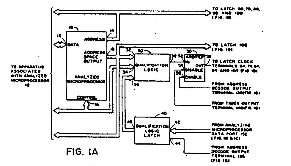
- Analyzed Microprocessor l0 ⁇ broadly illustrates a microprocessor whose operations are desired to be monitored.
- Microprocessor l0 ⁇ has associated therewith Data Port l2, Address Port l4, Control Port l6 and Address Space Output Port l8.
- Data Port l2 functions to provide a port through with data may be transferred between Analyzed Microprocessor l0 ⁇ and apparatus associated therewith.
- Address Port l4 functions to provide a port for Analyzed Microprocessor l0 ⁇ to indicate a desired address for an associated operation.
- Control Port l6 functions to provide a port for Analyzed Microprocessor l0 ⁇ to both send and receive control information associated with the operation thereof.
- Analyzed Microprocessor l0 ⁇ may have further functional ports associated therewith onto which Microprocessor l0 ⁇ may place additional information of interest. While such ports will vary among the different types of microprocessor devices, the function of such ports is broadly indicated in Figure lA by Address Space Outputs Port l8.
- Qualification Logic 30 ⁇ functions to compare two sets of information coupled thereto, and to provide an indication if the information contained within the two sets agree.
- Qualification Logic 30 ⁇ has associated therewith Qualification Logic Input Ports 32, 34 and 36, and Qualification Logic Output Terminal 38.
- the information coupled to Qualification Logic Input Ports 32 and 34 collectively, comprises the first set of information
- information coupled to Qualification Logic Input Port 36 comprises the second set of information.
- Qualification Logic 30 ⁇ compares the information from the first set of information, i.e., the information coupled to Qualification Logic Input Ports 32 and 34, with the information from the second set of information, i.e., the information coupled to Qualification Logic Input Port 36, and produces a single pulse on Qualification Logic Output Terminal 38 if the information contained within the two sets agrees. In a similar manner, when the information contained within the two sets of information does not agree, Qualification Logic 30 ⁇ produces no pulse on Qualification Logic Output Terminal 38. While there are many ways in which the functions of Qualification Logic 30 ⁇ may be implemented, Model l6L8A Integrated Circuits manufactured by Monolithic Memories, Inc.
- Qualification Logic Latch 40 ⁇ functions to receive information defining selected qualification conditions, and to store said qualification conditions for subsequent use by Qualification Logic 30 ⁇ , as more fully discussed hereafter.
- Qualification Logic Latch 40 ⁇ has associated therewith Qualification Logic Latch Input Port 42 and terminal 44, and Qualification Logic Latch Output Port 46.
- Qualification Logic Latch 40 ⁇ operates pursuant to the presence of an enabling signal on Qualification Logic Latch Input Terminal 44 to store the information which is present coincident therewith at Qualification Logic Latch Input Port 42. The information present at Qualification Logic Latch Input Port 42 will thereafter be continuously coupled to Qualification Logic Latch Output Port 46.
- Arbiter 50 ⁇ functions to selectively couple information present on an input terminal associated therewith to a corresponding output terminal.
- Arbiter 50 ⁇ has associated therewith Arbiter Input Terminal 52, Arbiter Disable Terminal 54, Arbiter Enable Terminal 56 and Arbiter Output Terminal 58.
- Arbiter 50 ⁇ will thereafter couple information present on Arbiter Input Terminal 52 to Arbiter Output Terminal 58.
- Arbiter 50 ⁇ will cease to couple information present on Arbiter Input Terminal 52 to Arbiter Output Terminal 58.
- Latch 60 ⁇ functions to temporarily store information coupled thereto, and thereafter, pursuant to a request, to couple the information previously stored therein to an output port associated therewith.
- Latch 60 ⁇ has associated therewith Latch Data Input Port 62, Latch Clock Terminal 64, Latch Output Enable Terminal 66 and Latch Data Output Port 68.
- Latch 60 ⁇ functions responsive to a pulse present at Latch Clock Terminal 64 to store the information present at Latch Data Input Port 62.
- Latch 60 ⁇ functions responsive to an enable signal on Latch Output Enable Terminal 66 to couple the information stored therein to Latch Data Output Port 68.
- Latches 70 ⁇ , 80 ⁇ , 90 ⁇ and l0 ⁇ 0 ⁇ have associated therewith Latch Data Input Ports 72, 82, 92, and l0 ⁇ 2, respectively, Latch Clock Terminal 74, 84, 94, and l0 ⁇ 4, respectively, Latch Output Enable Terminals 76, 86, 96 and l0 ⁇ 6, respectively, and Latch Data Output Port 78, 88, 98 and l0 ⁇ 8, respectively.
- Latches 70 ⁇ , 80 ⁇ , 90 ⁇ and l0 ⁇ 0 ⁇ function in an identical manner as was previously described with respect to Latch 60 ⁇ .
- Latches 60 ⁇ , 70 ⁇ , 80 ⁇ , 90 ⁇ and l0 ⁇ 0 ⁇ may be implemented, Model 74F374 Integrated Circuits manufactured by Fairchild Camera and Instrument Corporation are used in the preferred embodiment.
- the precise manner in which the foregoing described integrated circuits operate is more fully described in Fairchild Advanced Schottky TTL FAST Data Book , previously referenced.
- the manner in which these integrated circuits are configured to perform the aforedescribed functions of Latches 60 ⁇ , 70 ⁇ , 80 ⁇ , 90 ⁇ and l0 ⁇ 0 ⁇ would be apparent to one of ordinary skill in the art.
- Address Decode ll0 ⁇ functions to monitor information present on an address bus coupled thereto, and to produce individual signals in response to the occurrence of selected addresses on the address bus.
- Address Decode ll0 ⁇ has associated therewith Address Decode Output Terminals ll2, ll4, ll6, ll8, l20 ⁇ , l22, l24, l26, l28, l30 ⁇ and l32, Address Decode Control Input Port l34 and Address Decode Address Input Port l36.
- Address Decode ll0 ⁇ monitors information present at Address Decode Address Input Port l36, and in response to the occurrence of a selected address present at Address Decode Address Input Port l36, and corresponding control signals present at Address Decode Control Port Input l34, produces a corresponding signal on one of the associated Address Decode Output Terminals ll2, ll4, ll6, ll8, l20 ⁇ , l22, l24, l26, l28, l30 ⁇ or l32.
- Timer l40 ⁇ functions to provide a basic timing function. In particular, a selected period of time is first supplied to Timer l40 ⁇ . Thereafter, in response to a command to start, Timer l40 ⁇ will begin the timing of the selected time period. At the expiration of the selected time period, Timer l40 ⁇ will produce a signal indicating the expiration of the selected time period, and thereafter continuously repeat the process. Timer l40 ⁇ will continue to function in this fashion until stopped by a command coupled thereto. Timer l40 ⁇ has associated therewith Timer Data Port l42, Timer Load Terminal l44, Timer Read Terminal l46 and Timer Output Terminal l48. Functional commands, e.g.
- Timer l40 ⁇ commands to begin timing of the selected time period or to stop the aforedescribed timing operation, as well as the aforedescribed period of time, are coupled to Timer l40 ⁇ through Timer Data Port l42 coincident with an enabling signal on Timer Load Terminal l44.
- the time remaining within a time period may be determined by placing a signal on Timer Read Terminal l46 and sampling the data present at Timer Data Port l42.
- a Model 74LS593 Integrated Circuit manufactured by Texas Instruments, Inc. is used in the preferred embodiment. The precise manner in which the foregoing described integrated circuit operates is more fully described in The TTL Data Book, Vol 2,, Standard TTL, Schottky, and Low Power Schottky Circuits , Texas Instruments, l985, previously referenced.
- Analyzing Microprocessor l50 ⁇ functions to orchestrate the operations of the apparatus associated therewith in the monitoring of the activities of Analyzed Microprocessor l0 ⁇ ( Figure lA).
- Analyzing Microprocessor l50 ⁇ has associated therewith Data Port l52, Address Port l54, Control Port l56 and Interrupt Terminal l58.
- Data Port l52 functions to provide a port through with data may be transferred between Analyzing Microprocessor l50 ⁇ and apparatus associated therewith.
- Address Port l54 functions to provide a port for Analyzing Microprocessor l50 ⁇ to indicate a desired address for an associated operation.
- Control Port l56 functions to provide a port for Analyzing Microprocessor l50 ⁇ to both send and receive control information associated with an operation which it is performing.
- Interrupt Terminal l58 functions to provide a means of interrupting the operations of Analyzing Microprocessor l50 ⁇ with a request to perform a particular operation. In particular, the presence of a signal on Interrupt Terminal l58 will result in Analyzing Microprocessor l0 ⁇ completing the instruction which it is currently performing, and thereafter performing a desired sequence of instructions which function to accomplish a desired task, as will be more fully described hereinafter.
- ROM l60 ⁇ functions to provide information comprising a set of instructions which direct the operations of Analyzing Microprocessor l50 ⁇ .
- ROM l60 ⁇ has ROM Data Port l62, ROM Address Port l64, ROM Enable Terminal l66 and ROM Control Port l68 associated therewith.
- ROM l60 ⁇ functions to produce at ROM Data Port l62 the corresponding information stored at the location specified by the address at ROM Address Port l64.
- the set of instructions which are stored in ROM l60 ⁇ are described in more detail hereafter.
- ROM l60 ⁇ While there are many ways in which the functions of ROM l60 ⁇ may be implemented, Model 27256 EPROM Integrated Circuits manufactured by Intel Corporation of Santa Clara, CA are used in the preferred embodiment. The precise manner in which the referenced integrated circuits operate is more fully described in Memory Components Handbook , Intel Corporation, l985.
- RAM l70 ⁇ functions to provide for the temporary storage of information, i.e., to store information supplied thereto and subsequently to reproduce information previously stored therein.
- RAM l70 ⁇ has associated therewith RAM Data Port l72, RAM Address Port l74, RAM Enable Terminal l76 and RAM Control Port l78.
- RAM l70 ⁇ functions to either store information which is present at RAM Data Port l72 within RAM l70 ⁇ at the address which is present at RAM Address Port l74, or to extract information previously stored within RAM l70 ⁇ at the address which is currently present at RAM Address Port l74, and transfer said information to RAM Data Port l72, as determined by the associated control signal placed at RAM Control Port l78. While there are many ways in which the functions of RAM l70 ⁇ may be implemented, Model MMl256 Integrated Circuits manufactured by NEC Electronics Inc. of Mountain View, CA, are used in the preferred embodiment. The precise manner in which the referenced integrated circuits operate is more fully described in Memory Products l985 Data Book , NEC Electronics Inc., l985. The manner in which said integrated circuits would be configured would be apparent to one of ordinary skill in the art.
- Communications Interface l80 ⁇ functions to provide for the transfer of information between Analyzing Microprocessor l50 ⁇ and external apparatus which may desire to communicate therewith.
- external apparatus could include a wide variety of devices, including a terminal comprised of a display device and an accompanying keyboard, an information storage system, e.g., floppy or hard disk system, or a communication link to other information processing systems.
- Such types of external apparatus would depend upon the interfacing requirements of a particular application.
- Communications Interface l80 ⁇ has associated therewith Communication Interface Data Port l82, Communications Interface Address Port l84, Communications Interface Enable Terminal l86 and Communications Interface Control Port l88.
- the Communications Interface l80 ⁇ functions to either accept command information from Analyzing Microprocessor l50 ⁇ , or perform communication tasks, as defined by previous command information from Analyzing Microprocessor l50 ⁇ . While there are many ways in which the functions of Communications Interface l80 ⁇ may be implemented, a Model 825lA Programmable Communications Interface Integrated Circuit manufactured by Intel Corporation is used in the preferred embodiment. The precise manner in which the Programmable Communications Interface operates is more fully described in Microsystems Components Handbook, Microprocessors and Peripherals , Intel Corporation, l985. The manner in which the Programmable Communications Interface would be configured would be apparent to one of ordinary skill in the art.
- Address Port l4 of Microprocessor l0 ⁇ is further coupled to Latch Data Input Port 62, 72, 82 and 92 of Latch 60 ⁇ , 70 ⁇ , 80 ⁇ and 90 ⁇ ( Figure lB), respectively.
- the signals associated with Address Port l4 are typically divided into groups, with the signals comprising each group coupled to the individual latches, e.g., if each of Latch 60 ⁇ , 70 ⁇ , 80 ⁇ , 90 ⁇ and l0 ⁇ 0 ⁇ were capable of storing 8 bits of information, and there are a total of 32 signals associated with Address Terminal l4, address bits 0 ⁇ through 7 would be coupled to Latch Data Input Port 62 of Latch 60 ⁇ , address bits 8 through l5 would be coupled to Latch Data Input Port 72 of Latch 70 ⁇ , address bits l6 through 23 would be coupled to Latch Data Input Port 82 of Latch 80 ⁇ and address bits 24 through 3l coupled to Latch Data Input Port 92 of Latch 90 ⁇ .
- latch 60 ⁇ , 70 ⁇ , 80 ⁇ and 90 ⁇ are illustrated in Figure lB, it is to be understood that the present invention is not to be considered as limited to thereto. Rather, in accordance with the method and apparatus of the present invention, the number of latches which may be employed may be either increased or decreased to accommodate the signals associated with Address Port l4 of Analyzed Microprocessor l0 ⁇ .
- Control Port l6 of Analyzed Microprocessor l0 ⁇ is further coupled to the Input Port 34 of Qualification Logic 30 ⁇ .
- the information from Control Port l6 comprises part of the information which Qualification Logic 30 ⁇ will compare with the information coupled to Input Port 36, as more fully discussed hereafter.
- Address Space Output Port l8 functions to provide a port for further control information from Analyzed Microprocessor l0 ⁇ . Such control information may include additional information relating to the address information present at Address Port l4. It should be understood that the presence of Address Space Output Port l8 will vary depending upon the particular type of microprocessor that is being monitored, i.e., not all types of microprocessor have such Address Space Output Ports associated therewith. Address Space Output Port l8, if present, is coupled to Qualification Logic Input Port 32, as well as to Latch Data Input Port l0 ⁇ 2 ( Figure lB).
- Qualification Logic Input Port 32 and 34 are coupled to Address Space Output Port l8 and Control Port l6 of Analyzed Microprocessor l0 ⁇ , as previously discussed.
- Qualification Logic Input Port 36 is coupled to receive input data from Qualification Logic Latch Output Port 46.
- Qualification Logic Output Terminal 38 is coupled to Input Terminal 52 of Arbiter 50 ⁇ .
- Input Terminal 52 of Arbiter 50 ⁇ is coupled to Qualification Logic Output Terminal 38, as previously discussed.
- Arbiter Disable Terminal 54 is coupled to Output Terminal l48 of Timer l40 ⁇ ( Figure lB).
- Arbiter Enable Terminal 56 is coupled to Address Decode Terminal l20 ⁇ of Address Decode ll0 ⁇ ( Figure lB).
- Output Terminal 58 of Arbiter 50 ⁇ is coupled to Latch Clock Terminals 64, 74, 84, 94 and l0 ⁇ 4 of Latchs 60 ⁇ , 70 ⁇ , 80 ⁇ , 90 ⁇ and l0 ⁇ 0 ⁇ ( Figure lB).
- Input Port 42 of Qualification Logic Latch 40 ⁇ is coupled to Analyzing Microprocessor Data Port l52 ( Figure lB and lC).
- Qualification Logic Latch Input Terminal 44 is coupled to Address Decode Output Terminal l26 of Address Decode ll0 ⁇ ( Figure lB).
- Qualification Logic Latch Output Port 46 is coupled to Qualification Logic Input Port 36, as previously discussed.
- Latch Data Input Ports 62, 72, 82, and 92 of Latchs 60 ⁇ , 70 ⁇ , 80 ⁇ , and 90 ⁇ are coupled to selected signals from Address Port l4 of Analyzed Microprocessor l0 ⁇ ( Figure lA), as previously discussed.
- Latch Clock Terminals 64, 74, 84, 94 and l0 ⁇ 4 are coupled to Arbiter Output terminal 58 ( Figure lA), as previously discussed.
- Latch Data Output Ports 68, 78, 88, 98 and l0 ⁇ 8 are coupled to Analyzing Microprocessor Data Port l52 ( Figure lC).
- Latch Output Enable Terminals 66, 76, 86, 96 and l0 ⁇ 6 are coupled to Address Decode Output Terminals ll2, ll4, ll6, ll8 and l20 ⁇ , respectively.
- Address Decode Output Terminal l22 is coupled to Timer Read Terminal l46.
- Address Decode Output Terminal l24 is coupled to Timer Load Terminal l44.
- Address Decode Output Terminal l26 is coupled to Qualification Logic Latch Input Terminal 44 of Qualification Logic Latch 40 ⁇ ( Figure lA), as previously discussed.
- Address Decode Output Terminal l28 is coupled to ROM Enable Terminal l66 ( Figure lC).
- Address Decode Output Terminal l30 ⁇ is coupled to RAM Enable Terminal l76 ( Figure lC).
- Address Decode Control Port l34 is coupled to Analyzing Microprocessor Control Port l56 ( Figure lC).
- Address Decode Address Input Port l36 is coupled to Analyzing Microprocessor Address Port l54
- Timer Data Port l42 is coupled to Data Port l52 of Analyzing Microprocessor l50 ⁇ ( Figure lC).
- Timer Read Terminal l44 and Timer Load Terminal l46 are coupled to Address Decode Output Terminals l22 and l24, respectively, as previously discussed.
- Timer Output Terminal l48 is coupled to Arbiter Disable Terminal 54 ( Figure lA), as previously discussed, as well as to Interrupt Terminal l58 of Analyzing Microprocessor l50 ⁇ ( Figure lC).
- Data Port l52 of Analyzing Microprocessor l50 ⁇ is coupled to Latch Data Output Ports 68, 78, 88, 98 and l0 ⁇ 8 of Latches 60 ⁇ , 70 ⁇ , 80 ⁇ , 90 ⁇ and l0 ⁇ 0 ⁇ , respectively ( Figure lB), to Timer Data Port l42 ( Figure lB), to Qualification Logic Latch Input Port 42 ( Figure lA), as previously discussed, to ROM Data Port l62 of ROM l60 ⁇ , to RAM Data Port l72 and to Communication Interface Data Terminal l82.
- Address Port l54 of Analyzing Microprocessor l50 ⁇ is coupled to Address Decode Address Input Port l36 ( Figure lB), as previously discussed, to ROM Address Port l64, to RAM Address Terminal l74 and to Communication Interface ADdress Terminal l84.
- Control Port l56 of Analyzing Microprocessor l50 ⁇ is coupled to Address Decode Control Port l34 ( Figure lB), as previously discussed, to ROM Control Port l68, to RAM Control Port l78 and to Communication Interface Control Port l88.
- ROM l60 ⁇ ( Figure lC) functions to permanently store instructions which comprise the program which directs the operations of Analyzing Microprocessor l50 ⁇ .
- RAM l70 ⁇ ( Figure lC) functions to provide for the temporary storage of information for Analyzing Microprocessor l50 ⁇ , including counters associated with each of the user-specified address ranges, as more fully discussed hereafter, and any other data storage Analyzing Microprocessor l50 ⁇ may require.
- Analyzing Microprocessor l50 ⁇ receives instructions from ROM l60 ⁇ , and stores information temporarily in RAM l70 ⁇ . Prior to the monitoring of the operation of Analyzed Microprocessor l0 ⁇ ( Figure lA), Analyzing Microprocessor l50 ⁇ performs a number of initialization tasks, including the reading in of selected address and/or ranges of addresses through Communication Interface l80 ⁇ , and the storage of said information in RAM l70 ⁇ , initialization of user-selectable address ranges and their associated counters in RAM l70 ⁇ , initialization of Timer l40 ⁇ , both for the desired timing function as well as for the desired time period, and initialization of Qualification Logic Latch 40 ⁇ .
- initialization tasks including the reading in of selected address and/or ranges of addresses through Communication Interface l80 ⁇ , and the storage of said information in RAM l70 ⁇ , initialization of user-selectable address ranges and their associated counters in RAM l70 ⁇ , initialization of Timer l40 ⁇ , both for the desired timing function as
- Analyzing Microprocessor l50 ⁇ sequentially reads the contents of Latchs 60 ⁇ , 70 ⁇ , 80 ⁇ , 90 ⁇ and l0 ⁇ 0 ⁇ for the addresses of memory locations accessed by Analyzed Microprocessor l0 ⁇ , and thereafter determines the corresponding counters in RAM l70 ⁇ to increment, as more fully discussed hereafter.
- Input may also be received from a user in any of a wide variety of ways, such as a keyboard (not shown), through Communication Interface l80 ⁇ , in a manner well known to one of ordinary skill in the art.
- Address Decoder ll0 ⁇ ( Figure lB) functions to determine a unique address in the address space of Analyzing Microprocessor l50 ⁇ for each of Latches 60 ⁇ , 70 ⁇ , 80 ⁇ , 90 ⁇ and l0 ⁇ 0 ⁇ , ROM l60 ⁇ ( Figure lC), RAM l70 ⁇ ( Figure lC), Communications Interface l80 ⁇ ( Figure lC), Timer l40 ⁇ ( Figure lB) and Qualification Logic Latch 40 ⁇ ( Figure lA), thereby enabling Analyzing Microprocessor l50 ⁇ to individually access the various hardware blocks as necessary.
- Qualification Logic Latch 40 ⁇ ( Figure lA) is used to store the selected bus-cycle type of Analyzed Microprocessor l0 ⁇ during which addresses are to be stored in Latches 60 ⁇ , 70 ⁇ , 80 ⁇ , 90 ⁇ and l0 ⁇ 0 ⁇ ( Figure lB).
- the information stored in Qualification Logic Latch 40 ⁇ by Analyzing Microprocessor l50 ⁇ may correspond to a single cycle type or set of cycle types of Analyzed Microprocessor l0 ⁇ , thereby restricting the storage of addresses in Latches 60 ⁇ , 70 ⁇ , 80 ⁇ , 90 ⁇ and l0 ⁇ 0 ⁇ to addresses of a selected cycle-type.
- Qualification Logic Latch 40 ⁇ could be programmed by Analyzing Microprocessor l50 ⁇ for a bus-cycle type corresponding to only Bus Fetches, thereby restricting the storage of addresses in Latches 60 ⁇ , 70 ⁇ , 80 ⁇ , 90 ⁇ and l0 ⁇ 0 ⁇ to addresses accessed by Analyzed Microprocessor l0 ⁇ with a corresponding bus cycle of Bus Fetch.
- Qualification Logic 30 ⁇ operates to compare the current stored cycle-type of Analyzed Microprocessor l0 ⁇ , as defined by the information present on Qualification Logic Input Ports 32 and 34, with the cycle-types stored in Qualification Logic Latch 40 ⁇ , as defined by the information present on Qualification Logic Input Port 36. If a match occurs, a pulse is produced by Qualification Logic 30 ⁇ , which functions to effect the storage of a new address into Latches 60 ⁇ , 70 ⁇ , 80 ⁇ , 90 ⁇ and l0 ⁇ 0 ⁇ , subject to control of Arbiter 50 ⁇ .
- Arbiter 50 ⁇ functions to prevent conflicts between the storage of information into Latches 60 ⁇ , 70 ⁇ , 80 ⁇ , 90 ⁇ and l0 ⁇ 0 ⁇ and the reading of information therefrom by Analyzing Microprocessor l50 ⁇ , i.e., to prevent the changing of information in the latches during the reading of the contents thereof by Analyzing Microprocessor l50 ⁇ .
- the indication produced by Qualification Logic 30 ⁇ indicating a match functions to effect the storage of address information from Analyzed Microprocessor l0 ⁇ as present at Address Port l4 into Latches 60 ⁇ , 70 ⁇ , 80 ⁇ , 90 ⁇ and l0 ⁇ 0 ⁇ .
- Latches 60 ⁇ , 70 ⁇ , 80 ⁇ , 90 ⁇ and l0 ⁇ 0 ⁇ are the primary link between Analyzed Microprocessor l0 ⁇ and Analyzing Microprocessor l50 ⁇ .
- the input Ports of Latches 60 ⁇ , 70 ⁇ , 80 ⁇ , 90 ⁇ and l0 ⁇ 0 ⁇ are coupled to address information produced by Analyzed Microprocessor l0 ⁇ .
- the number of latches is determined by the particular type of microprocessor which is desired to be monitored, e.g., the particular type of device corresponding to Analyzed Microprocessor l0 ⁇ .
- each of Latches 60 ⁇ , 70 ⁇ , 80 ⁇ , 90 ⁇ and l0 ⁇ 0 ⁇ is capable of storing a single byte, i.e., 8 bits, of the address information.
- Analyzing Microprocessor l50 ⁇ programs a value corresponding to a desired time interval between measurements into Timer l40 ⁇ . Thereafter, responsive to a command from Analyzing Microprocessor l50 ⁇ , Timer l40 ⁇ begins counting, and the analysis of the performance of Analyzed Microprocessor l0 ⁇ begins. When the time interval expires, Timer l40 ⁇ generates an interrupt to Analyzing Microprocessor l50 ⁇ , reloads itself, and begins counting the desired time interval again. During the timing of the next interval, Analyzing Microprocessor l50 ⁇ reads the information stored in each of Latches 60 ⁇ , 70 ⁇ , 80 ⁇ , 90 ⁇ and l0 ⁇ 0 ⁇ .
- Analyzing Microprocessor l50 ⁇ compares the address read from said latches with each of the address ranges it has been previously programmed to monitor, and increments the counter in RAM l70 ⁇ which corresponds to the address or address range in which the address read from the latches falls. Analyzing Microprocessor l50 ⁇ also increments another counter which counts the total number of samples. Thereafter, Analyzing Microprocessor l50 ⁇ waits for the next interrupt from Timer l40 ⁇ , and repeats the above described process.
- Figures 2A, 2B and 2C broadly illustrate functional steps performed by Analyzing Microprocessor l50 ⁇ .
- Figures 3A, 3B and 3C illustrate the basic operations which sequentially occur with respect to Analyzing Microprocessor l50 ⁇ , Timer l40 ⁇ , Latches 60 ⁇ , 70 ⁇ , 80 ⁇ , 90 ⁇ and l0 ⁇ 0 ⁇ , and Analyzed Microprocessor l0 ⁇ .
- Analyzing Microprocessor l50 ⁇ ( Figure lC) first performs initialization of any hardware which may be associated therewith, as illustrated generally by block 20 ⁇ 0 ⁇ .
- Such initialization routines would include the reading of information from Communications Interface l80 ⁇ for both operational instructions as well as data to be used in connection with the monitoring operation.
- individual and/or ranges of addresses contained within the address space of Analyzed Microprocessor l0 ⁇ are first selected for monitoring, according to selected qualification information. This information, received through Communication Interface l80 ⁇ is transferred to RAM l70 ⁇ by Analyzing Microprocessor l50 ⁇ during the initialization routines.
- the address information must be stored in a particular manner within RAM l70 ⁇ , and consequently requires processing to arrange said address information in a required format prior to storage within RAM l70 ⁇ , as will be more fully discussed hereafter. It will be recognized by one skilled in the art that the required processing of the address information could be performed either prior to transfer to Analyzing Microprocessor l50 ⁇ , or by Analyzing Microprocessor l50 ⁇ subsequent to the transfer thereto.
- the interval of time associated with required initialization operations is illustrated in Figure 3A as time period Tl.
- Timer l40 ⁇ is stopped, i.e., Timer l40 ⁇ is not counting, Latches 60 ⁇ , 70 ⁇ , 80 ⁇ , 90 ⁇ and l0 ⁇ 0 ⁇ are not acquiring information, and Analyzed Microprocessor l0 ⁇ is stopped, i.e., Analyzed Microprocessor l0 ⁇ is not performing the execution of instructions from a program.
- the instructions for such initialization, as well as other instructions comprising the program which Microprocessor l50 ⁇ executes are stored in ROM l60 ⁇ .
- Microprocessor l50 ⁇ requests information from ROM l60 ⁇ by placing the address of a location within ROM l60 ⁇ containing desired information on Address Port l54, along with appropriate control signals on Control Port l56.
- Address Decode ll0 ⁇ in response thereto functions to produce an enable signal on Address Decode Output Terminal l28.
- ROM l60 ⁇ responsive to the enable signal produced by Address Decode ll0 ⁇ , the information coupled to ROM Address Port l64 and ROM Control Port l68, operates to transfer the information previously stored in the location specified by the information at ROM Address Port l64 to ROM Data Port l62.
- Analyzing Microprocessor l50 ⁇ thereafter operates to read the information present at Data Port l52, thereby obtaining the information stored in the address location of ROM l60 ⁇ which was previously at Address Port l54.
- the foregoing described process repeats with respect to each location contained within ROM l60 ⁇ for which the information stored therein is desired to be read.
- Analyzing Microprocessor l50 ⁇ has completed the foregoing described initialization.
- Analyzing Microprocessor l50 ⁇ initializes the locations in RAM l70 ⁇ which will be used for counting purposes, to a value of zero, as illustrated in block 20 ⁇ 2 ( Figure 2A). This is done by Microprocessor l50 ⁇ writing a zero value to each of these locations. Microprocessor l50 ⁇ communicates with locations in RAM l70 ⁇ in a similar manner as was previously described with respect to ROM l60 ⁇ through an enable signal produced on Address Decode Output Terminal l30 ⁇ and coupled to RAM Enable Terminal l76. The initialization of the locations in RAM l70 ⁇ which will be used for counting purposes occurs during time period T2 ( Figure 3A).
- Microprocessor l50 ⁇ performs the necessary initialization associated with Timer l40 ⁇ ( Figure lB), as illustrated by block 20 ⁇ 4 of Figure 2A. Such initialization process typically includes not only sending command information to place Timer l40 ⁇ in a desired mode of counting, but also includes sending to Timer l40 ⁇ the desired timing period. Analyzing Microprocessor l50 ⁇ ( Figure lC) communicates command information to Timer l40 ⁇ by transferring the address of Timer l40 ⁇ to Address Port l54, the corresponding command or data information at Data Port l52, and the corresponding control signals at Control Port l56.
- Address Decode ll0 ⁇ responsive the information on Address Port l54 and Control Port l56 will operate to produce an enable signal on Terminal l24 of Address Decode ll0 ⁇ .
- Timer l40 ⁇ responsive to the enable signal on Timer Load Terminal l44 from Address Terminal l24 will operate to read the information concurrently present at Timer Data Port l42, thereby coupling the information from Data Port l52 of Microprocessor l50 ⁇ to Timer l40 ⁇ .
- the initialization associated with Timer l40 ⁇ occurs during time period T2 ( Figure 3A).
- Analyzing Microprocessor l50 ⁇ performs the necessary initialization associated with Qualification Logic Latch 40 ⁇ ( Figure lA), as illustrated by block 20 ⁇ 6 of Figure 2A.
- Such initialization operates to specify the particular type of activity which is of interest to monitor with respect to the addresses accessed by Analyzed Microprocessor l0 ⁇ .
- Such information could vary in scope, from the monitoring of any type of accesses, e.g., either a read or write to an address, to more limited monitoring, e.g., read-only operations.
- Qualification Logic Latch 40 ⁇ could be programmed to monitor any type of activity which may occur with respect to addresses associated with Microprocessor l0 ⁇ which may occur, as defined by control information present on Control Port l6 and Address Space Output Port l8 of Analyzed Microprocessor l0 ⁇ . Analyzing Microprocessor l50 ⁇ effects the initialization of Qualification Logic Latch 40 ⁇ by placing the desired qualification information on Data Port l52, the address associated with Qualification Logic Latch 40 ⁇ on Address Port l54, and the corresponding control signals on Control Port l56.
- Timer l40 ⁇ is stopped, Latches 60 ⁇ , 70 ⁇ , 80 ⁇ , 90 ⁇ and l0 ⁇ 0 ⁇ are not acquiring data, and Analyzed Microprocessor l0 ⁇ is stopped.
- Analyzed Microprocessor l0 ⁇ is started, i.e., Analyzed Microprocessor l0 ⁇ is allowed to begin executing instructions of the program which is desired to be monitored. This is illustrated in block 20 ⁇ 8 ( Figure 2A).
- Timer l40 ⁇ is stopped, Latches 60 ⁇ , 70 ⁇ , 80 ⁇ , 90 ⁇ and l0 ⁇ 0 ⁇ are not acquiring data, and Analyzed Microprocessor l0 ⁇ is executing the instructions of the program which is desired to be monitored.
- Analyzing Microprocessor l50 ⁇ issues a command to Timer l40 ⁇ to begin the timing operation, i.e., begin timing of the pre-selected time interval. This is illustrated in block 2l0 ⁇ ( Figure 2A). Analyzing Microprocessor l50 ⁇ initiates the operation of Timer l40 ⁇ by issuing a start command to Timer l40 ⁇ , in an manner identical to that previously discussed with respect to the initialization of Timer l40 ⁇ . The issuing of a command to Timer l40 ⁇ by Analyzing Microprocessor l40 ⁇ defines the end of time period T3, and the beginning of time period T4 ( Figure 3B).
- Analyzing Microprocessor l50 ⁇ enables Arbiter 50 ⁇ ( Figure lA) as indicated in block 2l2 ( Figure 2A),i.e., an enable signal is coupled to Arbiter Enable Terminal 56, thereby enabling information coupled to Arbiter Input Terminal 52 to appear on Arbiter Output Terminal 58.
- Analyzing Microprocessor l50 ⁇ enables Arbiter 50 ⁇ by placing the address associated with the last latch which is read during the process of reading the group of latches, i.e., Latch l0 ⁇ 0 ⁇ , on Address Port l54 and corresponding control information on Control Port l56.
- Address Decode ll0 ⁇ responsive to information at Address Decode Control Port l34 and Address Decode Address Input Port l36 functions to produce a corresponding enable signal on Address Decode Output Terminal l20 ⁇ .
- Arbiter 50 ⁇ responsive to an enable signal on Arbiter Enable Terminal 56 functions to couple information present on Arbiter Input Terminal 52 to Arbiter Output Terminal 58.
- the enabling of Arbiter 50 ⁇ marks the conclusion of time period T4.
- Timer l40 ⁇ is counting, Latches 60 ⁇ , 70 ⁇ , 80 ⁇ , 90 ⁇ and l0 ⁇ 0 ⁇ are not acquiring addresses, and Analyzed Microprocessor l0 ⁇ is executing the program under test.
- Analyzed Microprocessor l0 ⁇ has begun execution of instructions contained in the program whose execution by Analyzed Microprocessor l0 ⁇ is desired to be monitored, Timer l40 ⁇ has begun timing of the desired time interval, and Latches 60 ⁇ , 70 ⁇ ,, 80 ⁇ , 90 ⁇ and l0 ⁇ 0 ⁇ are storing information from Address Port l4 of Analyzed Microprocessor l0 ⁇ .
- Analyzing Microprocessor l50 ⁇ waits for a signal from Timer l40 ⁇ indicating the that previously discussed time period has expired. This is typically achieved by looping instructions contained within the program which Analyzing Microprocessor l50 ⁇ is executing. The return to these looping instructions is broadly indicated by block 2l4 ( Figure 2A).
- Analyzing Microprocessor l50 ⁇ is waiting for the interrupt signal produced by Timer l40 ⁇ on Timer Output Terminal l48 ( Figure lB), Timer l40 ⁇ is counting, Latches 60 ⁇ , 70 ⁇ , 80 ⁇ , 90 ⁇ and l0 ⁇ 0 ⁇ are acquiring qualified addresses, and Analyzed Microprocessor l0 ⁇ is executing the program under test.
- Analyzed Microprocessor l0 ⁇ ( Figure lA) is executing instructions contained in the program under test, during which process Analyzed Microprocessor l0 ⁇ typically transfers various addresses to Address Port l4 along with corresponding control information on Control Port l6 and Address Space Output Port l8.
- Qualification Logic 30 ⁇ functions to compare the corresponding control information, i.e., the corresponding information Analyzed Microprocessor l0 ⁇ has received at Control Port l6 and transferred to Address Space Output Port l8 with the qualifying information coupled to Qualification Logic Input Port 36 by Qualification Logic Latch 40 ⁇ .
- Timer l40 ⁇ At the expiration of the pre-selected time period, Timer l40 ⁇ produces an indication thereof on Timer Output Terminal l48, and again begins timing of the pre-selected time period, as illustrated in block 2l6 ( Figure 2B).
- the indication produced by Timer l40 ⁇ is coupled to both Arbiter Disable Terminal 54 and Interrupt Terminal l58 of Analyzing Microprocessor l50 ⁇ , as previously discussed.
- Timer Output Terminal l48 As the indication produced on Timer Output Terminal l48 is coupled to Arbiter Disable Terminal 54, the indication produced by Timer l40 ⁇ operates to inhibit the further coupling of any pulse coupled from Arbiter Input Terminal 52 to Arbiter Output Terminal 58. As a consequence thereof, the contents of Latches 60 ⁇ , 70 ⁇ , 80 ⁇ , 90 ⁇ and l0 ⁇ 0 ⁇ will remain static, allowing the asychronous reading by Analyzing Microprocessor l50 ⁇ of the last address information stored therein. The occurrence of the signal from Timer l40 ⁇ , i.e., the receipt of the interrupt by Analyzed Microprocessor l50 ⁇ marks the completion of time period T5, and the start of time period T6.
- Timer Output Terminal l48 is also coupled to Interrupt Terminal l58
- Analyzing Microprocessor l50 ⁇ is interrupted from the previously described wait loop, and thereafter reads address information from Latches 60 ⁇ , 70 ⁇ , 80 ⁇ , 90 ⁇ and l0 ⁇ 0 ⁇ , increments a counter which functions to count the total number of times the contents of Latches 60 ⁇ , 70 ⁇ , 80 ⁇ , 90 ⁇ and l0 ⁇ 0 ⁇ were read by Analyzing Microprocessor l50 ⁇ , compares the value of the address read from said latch against the pre-selected ranges of addresses which have had counters established therefor in RAM l70 ⁇ ( Figure lC), and increments the corresponding counter.
- Analyzing Microprocessor l50 ⁇ reads the contents of Latches 60 ⁇ , 70 ⁇ , 80 ⁇ , 90 ⁇ and l0 ⁇ 0 ⁇ , as broadly indicated in block 2l8 ( Figure 2B). As each of Latches 60 ⁇ , 70 ⁇ , 80 ⁇ , 90 ⁇ and l0 ⁇ 0 ⁇ contain a portion of the address information, each latch is separately read. Analyzing Microprocessor l50 ⁇ ( Figure lC) first reads the contents of Latch 60 ⁇ ( Figure lB) by transferring the address thereof to Address Port l54 of Analyzing Microprocessor l50 ⁇ along with corresponding control information to Control Port l56.
- Address Decode ll0 ⁇ ( Figure lB), responsive to said information from Analyzing Microprocessor l50 ⁇ at Address Decode Control Port l34 and Address Decode Address Input Port l36 operates to produce an enable signal on Address Decode Output Terminal ll2.
- Latch 60 ⁇ responsive to said enable signal from Address Decode ll0 ⁇ on Latch Output Enable Terminal 66 functions to transfer the information stored therein to Latch Data Output Port 68.
- Analyzing Microprocessor ll0 ⁇ thereafter reads the information from Latch Data Output Port 68 at Data Port l52.
- the contents of Latches 70 ⁇ , 80 ⁇ , 90 ⁇ and l0 ⁇ 0 ⁇ are read by Analyzing Microprocessor l50 ⁇ .
- Timer l40 ⁇ is counting, Address Latches 60 ⁇ , 70 ⁇ , 80 ⁇ , 90 ⁇ and l0 ⁇ 0 ⁇ are holding the last acquired address, and Analyzed Microprocessor l0 ⁇ is executing the program under test.
- Analyzing Microprocessor l50 ⁇ again enables Latches 60 ⁇ , 70 ⁇ , 80 ⁇ , 90 ⁇ and l0 ⁇ 0 ⁇ for the storage of address information by enabling the coupling of information from Arbiter Input Terminal 52 to Arbiter Output Terminal 58 ( Figure lA), as indicated by block 220 ⁇ ( Figure 2B).
- Analyzing Microprocessor l50 ⁇ places the corresponding address of the last latch contained in the group of latches, i.e., Latch l0 ⁇ 0 ⁇ , on Address Terminal l54 along with corresponding information on Control Terminal l56.
- Address Decode ll0 ⁇ responsive to the information from Analyzing Microprocessor l50 ⁇ at Address Decode Control Port l34 and Address Decode Address Input Port l36 operates to produce a corresponding enable signal on Address Decode Output Terminal l20 ⁇ .
- the enable signal produced on Address Decode Output Terminal l20 ⁇ of Address Decode ll0 ⁇ is coupled to both Latch Output Enable Terminal l0 ⁇ 6 of Latch l0 ⁇ 0 ⁇ and Arbiter Enable Terminal 54 of Arbiter 50 ⁇ , the reading of the information contained in the last latch, i.e., Latch l0 ⁇ 0 ⁇ , operates to produce an enable signal on Arbiter Enable Terminal 56.
- Arbiter 50 ⁇ thereafter again couples information from Arbiter Input Terminal 52 to Arbiter Output Terminal 58. Thereafter, responsive to control information from Analyzed Microprocessor l0 ⁇ agreeing with the information previously stored in Qualification Logic Latch 40 ⁇ (block 20 ⁇ 6 of Figure 2A), information appearing at Address Port l4 of Analyzed Microprocessor l0 ⁇ will again be stored in Latches 60 ⁇ , 70 ⁇ , 80 ⁇ , 90 ⁇ and l0 ⁇ 0 ⁇ , as previously discussed. As the reading of the contents of the latches by Analyzing Microprocessor l50 ⁇ occurs during time period T6, the production of the foregoing described enable signal to Arbiter 50 ⁇ occurs at the end of time period T6 ( Figure 3B).
- Analyzing Microprocessor l50 ⁇ increments the number of times which address information has been observed, i.e., the number of times the contents of Latches 60 ⁇ , 70 ⁇ , 80 ⁇ , 90 ⁇ and l0 ⁇ 0 ⁇ has been collectively read, as indicated in block 220 ⁇ ( Figure 2B).
- Analyzing Microprocessor l50 ⁇ compares the address read against the previously specified ranges of addresses of interest, as indicated in block 224 ( Figure 2B). If the address which was read from the latches is found to fall within one of the specified ranges, a count indication is produced, i.e., the counter associated with that range is incremented, as indicated in block 226.
- the aforedescribed searching and incrementing process occurs during time period T7 ( Figure 3B).
- Timer l40 ⁇ is counting, Latches 60 ⁇ , 70 ⁇ , 80 ⁇ , 90 ⁇ and l0 ⁇ 0 ⁇ are acquiring qualified addresses, and Analyzed Microprocessor l0 ⁇ is executing the program under test.
- Analyzing Microprocessor l50 ⁇ again returns to the aforedescribed wait loop, as indicated in block 228 ( Figure 2B). At this point Analyzing Microprocessor l50 ⁇ will check to see if the foregoing described process should be repeated or if the analysis of Analyzed Microprocessor l0 ⁇ is completed, as indicated in Block 229.
- Timer l40 ⁇ will again produce an indication thereof on Timer Output Terminal l48, and the above described process will repeat, i.e., the operations discussed with respect to blocks 2l6, 2l8, 220 ⁇ , 222, 224, 226 and 228 of Figure 2B. If however, the analysis of Analyzed Microprocessor l0 ⁇ is completed, then Analyzing Microprocessor l50 ⁇ next performs step 230 ⁇ ( Figure 2C), as more fully described hereafter.
- Analyzed Microprocessor l0 ⁇ would be considered as completed would vary depending upon the nature of the desired analysis, and could include monitoring for selected intervals of time, or until selected events occurring external to Analyzed Microprocessor l0 ⁇ have occurred.
- Timer l40 ⁇ is first stopped in step 230 ⁇ by Analyzing Microprocessor l50 ⁇ . This is performed by issuing a command to Timer l40 ⁇ to effect the stopping of its operation, in a manner as was previously described with respect to communicating commands thereto by Analyzing Microprocessor l50 ⁇ .
- step 240 ⁇ the information which was obtained as a result of the foregoing described data collection activity is processed in accordance with the particular requirements associated with the analysis process.
- processing of collected information would vary depending upon the desired processing activity, and could include not only the formatting of the information in tabular or graphic format, but further statistical processing according to techniques well known to one skilled in the art.
- step 250 ⁇ Thereafter the results of the data collection and processing are displayed in step 250 ⁇ , and again would vary depending upon the nature of the display desired. While such display would typically include the display of the results in a visual format, i.e., in either a tabular or graphic format, such display step could likewise include the transfer of the resulting information to a suitable storage medium, i.e., floppy or hard disk, or transmission to other data processing or storage devices.
- a suitable storage medium i.e., floppy or hard disk
- step 260 ⁇ Analyzing Microprocessor l50 ⁇ would again return to the aforedescribed wait loop.
- T6 comprises the reading of information from Latches 60 ⁇ , 70 ⁇ , 80 ⁇ , 90 ⁇ and l0 ⁇ 0 ⁇ , as more fully discussed with respect to block 2l8 of Figure 2B, it is clear that the time required for this operation is directly dependent upon the amount of information which Analyzing Microprocessor l50 ⁇ may access via Data Port l52 during a single read operation.
- Data Port l52 is eight bits wide, then eight bits is the maximum amount of information which may be read in by Analyzing Microprocessor l50 ⁇ during a single read operation, and consequently operates to define the maximum size of the associated latches, i.e., Latches 60 ⁇ , 70 ⁇ , 80 ⁇ , 90 ⁇ and l0 ⁇ 0 ⁇ .
- Data Port l52 is sixteen bits wide, then sixteen bits may be read during a single read operation, and each of the corresponding latches may be comprised of the same number of bits, thereby decreasing the time required to perform the operation which occurs during time period T6.
- the information previously discussed with respect to the counter locations in RAM l70 ⁇ is stored as an array of records, with each record containing three fields: a low address field, a high address field, and a counter field.
- the record number of the data array will hereafter be referred to as the index.
- the index of the first record in memory will be one, the second record two, etc.
- the low address field is the lower bound which a matched address must be greater than or equal to, to qualify as a match.
- the high address field is the upper bound which a matched address must be less than or equal to, to qualify as a match.
- the counter field contains the number of times a sampled address fell within the range defined by the lower and upper bounds of the record.
- each of the address ranges must be exclusive of each of the other address ranges, i.e., a selected address must belong to one and only one address range.
- each address range must have a non-negative distance between the low address and the high address, i.e., the address contained in the low address field must in fact be less than or equal to the address contained in the high address field.
- the array of records is a position oriented, in-order binary tree.
- the tree is sorted with the range as the key. As each range is exclusive of all other ranges, each range has an unambiguous relationship with all the other ranges in the array.
- the binary array must be packed, i.e., the binary tree must fill up the array without any empty elements, except at the end of the array.
- all elements of the array are used in a linear fashion so that an entire non-empty tree fits within positions of the array indexed by one through n, and none of positions one through n is empty. It is consequently necessary that the pre-selected range of addresses be properly placed in the foregoing described data array within RAM l70 ⁇ . While there are many ways in which this may be accomplished, the algorithm employed in the preferred embodiment is given in Table l below.
- an index counter is initially set equal to one in block 270 ⁇ . Thereafter, in block 272, the value of the index is checked to see if it exceeds the end of the array. If the value of the index does exceed the end of the array, then Analyzing Microprocessor l50 ⁇ returns to the previously described wait loop to await the next interrupt from Timer l40 ⁇ , as indicated in block 274.
- Analyzing Microprocessor l50 ⁇ computes a new index, as illustrated in block 278.
- the value of the new index is determined by multiplying the value of the current index by two and adding one to the result. Thereafter, Analyzing Microprocessor returns and again performs the function previously discussed with respect to block 272.
- the value of the address read from the latches is compared with the value of the address contained in the low address field of the record, as illustrated in block 280 ⁇ . If the value of the address read from the latches is less than the value of the address contained in the low address field of the record, then Analyzing Microprocessor l50 ⁇ computes a new index in block 282 by multiplying the current value of the index by two. Thereafter, Analyzing Microprocessor l50 ⁇ again returns and performs the operations previously discussed with respect to block 272.
- time period T6 may be minimized by choosing a microprocessor to implement the functions of Analyzing Microprocessor l50 ⁇ having a maximum number of data lines associated with Data Port l54, as previously discussed. While the time required for time period T7 is significantly reduced by employing the foregoing described data structure and accompanying search method, time period T7 may be minimized by reducing the number of instructions required to perform the search and increment operation previously discussed. In the preferred embodiment, this was accomplished by minimizing the number of machine language statements produced by the compiling of the program of Table 2, and is given below in Table 3 for the Motorola 690 ⁇ 0 ⁇ 8L8 microprocessor.
- the information in the array is arranged so that the array is filled without any empty elements, except at the end of the array. Consequently all elements of the array are used in a linear fashion so that an entire non-empty array fits within positions of the array indexed by l through n, and none of positions l through n is empty.
- This condition is known as a packed binary tree.
- the maximum number of pre-selected address ranges which may be searched is exponentially related to the level of the binary tree. In particular, as the level of the binary tree increases, the number of address ranges which can be searched increases by two raised to an exponential power, equal to the level of the binary tree.
- each address or range of address specified in the initialization phase will have a percentage of total execution time attributed to it.
- the amount of time spent in other addresses, besides the ones specified at initialization, will have a single precentage of execution time attributed to them collectively.
Abstract
Description
- This invention relates to monitoring devices, and more particularly to a method and apparatus for monitoring the operation of a processor without interrupting or altering the normal real-time functions, behavior or operational environment associated therewith.
- Broadly speaking, a processor operates by sequentially performing a set of instructions, generally referred to as a program. The program is designed to accomplish an objective, and may reference additional information, generally referred to as data, in accomplishing the objective.
- A processor may be considered as fundamentally comprising a central processing unit and a memory unit. The central processing unit basically performs desired operations pursuant to the program and data which are stored in the associated memory unit. Typically the memory unit is comprised of many sequential unique storage locations, each of which is capable of storing a unit of information. In this regard, it should be particularly noted that the units of information stored in the memory may be either instructions to direct the operations of the central processing unit, i.e., the program, or data which will be operated upon by the central processssing unit pursuant to the instructions.
- As processors and the associated programs are complex devices, it is frequently desirable to monitor the operations of a processor, especially during the design and development of apparatus employing a processor, or the design and development of assciated programs. This has been accomplished in a number of ways.
- In the past when central processing units were fabricated using discrete components, the contents of various registers and the status of various operations which occurred internal to the central processing unit were typically displayed by a collection of indicating devices. In some designs, each indicating device was permanently associated with a particular functional part within the central processor, and would continuously display the associated information. This frequently resulted in a large collection of indicating devices of various types. Such an approach frequently further included additional monitoring apparatus, such as instruction execution control devices. Such devices operated to provide such functions as controlling the rate at which the central processing unit performed the execution of individual instructions in a program, or halting the execution of instructions upon the occurrence of predefined conditions. When it was desirable to study a particular internal operation of a central processing unit not available through dedicated monitoring devices, specialized monitoring equipment was attached to selected points within the central processing unit. By way of example, if an analysis of the performance of a central processing unit in the execution of a particular program was of interest, the details of the particular program and associated parts of the central processing unit would be closely examined. In particular, the information of interest with respect to the program would first be determined. Thereafter, the associated apparatus within the central processor would be determined by a close examination of the internal architecture and operation of the central processing unit to determine the appropriate signals within the central processing unit which would contain the information of interest. Thereafter, signal probes would be attached to appropriate points within the internal circuity of the central processing unit to monitor the particular signals of interest. With the signal probes in place, the program of interest would then be run, and the information of interest collected. The information received via the signal probes would then be processed according the requirements of the monitoring task, and recorded for subsequent analysis. By employing such an approach, the desired details with respect to the operational characteristics of the central processing unit in the performance of a particular program could be determined.
- Approaches employing dedicated indicating and monitoring devices offer a number of advantages, the most significant of which provides the capability of monitoring the operation of a central processing unit without disturbing the environment in which a program may be executing. However, with the advent of the fabrication of central processing units as integrated circuits, and the accompanying limitations associated with integrated circuit packaging techniques, it has not been possible to use dedicated indicating and monitoring devices to monitor the internal operation of a central processing unit fabricated as an integrated circuit. This limitation primarily results from the physical constraint of being unable to route the large number of electrical conductors necessarily associated with dedicated indicating devices out of the integrated circuit package. With advances in the design of central processing units, the physical limitations imposed by integrated circuit packaging techniques have become even more limiting, and in some applications have operated to require multiplexing techniques to make the necessary signals available. This situation naturally makes the monitoring of the activities which occur internal to the central processing unit accordingly more difficult.
- In response to the limitations imposed by integrated circuit packaging techniques, and the desire to monitor operations of a central processing unit, a number of alternate approaches have been taken. One such approach has been based upon programming, or software techniques, and a second approach has been based upon hardware techniques.
- In the software, or programming technique, the central processing unit has been used to monitor itself. In such an approach, a program is entered on a periodic basis to tabulate the current execution state of a machine. Broadly stated, in such an approach, the machine not only operates to execute a program of interest, but also to perform monitoring functions associated therewith. Such an approach is frequently based upon techinques which include monitoring the status of the time allocated to execution of the program of interest by an associated operating system.
- However, notwithstanding the advantages presented by using such programming or software techniques, such an approach has an inherent shortcoming fundamental to the process. In particular, the basic environment existing during the execution of program instructions is disturbed. This follows from the fact that the central processing unit must not only execute the program of interest, but must also execute the monitor program. By so executing the monitor program, the central processing unit is performing tasks that it otherwise would not do if it were executing the program alone. Such a shortcoming can present disadvantages of varying scope. One such disadvantage is in the time required for the execution of the program of interest. Since the central processing unit is having to execute both the program of interest as well as the monitor program, additional execution time is clearly required. While this may be acceptable under some conditions, it can be most undesirable under others. In particular, in an application in which it is desired to monitor an environment wherein the central processing unit must not only execute a program of interest, but must also respond to events which are occurring external to the central processing unit, the imposing upon the central processing unit of the additional task of executing the monitor program can significantly alter the basic environment which is desired to be monitored. This result follows from the fact that the time which the central processing unit would otherwise dedicate to the program of interest and responding to events which are occurring external to the central processing unit is reduced by the amount of time required by the central processor to perform the appropriate portions of the monitor program. Consequently such an approach has the serious shortcoming of disturbing the environment which is desired to be monitored.
- Hardware monitoring techniques are generally based upon the monitoring of the signals produced by a central processing unit. Broadly speaking, the signals associated with a central processing unit fabricated as an integrated circuit can be classified into three groups: control signals, address signals and data signals. These signals function to electrically interface the central processing unit with the components associated therewith. Consequently, monitoring these signals can provide some indication of the operations occurring within the central processor unit.
- In one approach, the address signals from the central processing unit are segregated into two groups, and each address signal present within each group is assigned a particular binary weight. Thereafter, a corresponding analog signal is derived for each of the signal groups having a magnitude proportional to the binary weight of the signal present on the address lines within each of the two groups. This is generally accomplished through the use of digital-to-analog converter devices. Thereafter, the two analog output signals are used to control the horizontal and vertical deflection plates of an oscilloscope. The resulting display on the oscilloscope will consequently provide some information with respect to the location in memory wherein the central processing unit is currently active. While such an approach does offer the advantage of not disturbing the operational environment within the central processing unit, the information so provided with respect to the internal operation of the central processing unit is very limited.
- More advanced hardware monitoring approaches are employed in logic analyzer type devices. In particular, signal probes associated with a logic analyzer are coupled to receive the signals produced by a microprocessor: the control signals, the address signals and the data signals. The logic analyzer then operates to monitor the foregoing signals. The information obtained from such monitoring process can be either recorded for subsequent analysis, or used to immediately identify selected conditions.
- In one approach used with respect to logic analyzers, it is possible to use associated hardware word recognizers to respond to addresses within a given range. Each word recognizer would be associated with a user-selectable range of addresses. In addition, a counter associated with each word recognizer is used to count each time its word recognizer responds to an address within its range. In practice, each of the word recognizers would be programmed to respond to different ranges of addresses, and when monitoring the analyzed microprocessor, would increment associated counters upon recognition of a vaild address. At the conclusion of the measurement, the contents of the counters would be examined and the results presented to the users. The disadvantage of this method is that only a limited number of address ranges can be examined at one time, because additional hardware is required for each of the ranges.
- The foregoing hardware examples are but a few of the approaches which have been employed in the past to gain insight on the operations of a central processing unit by monitoring the various signals associated therewith. It will be observed that while each approach shares the common advantage of not disturbing the operation of a program within the central processing unit, the information provided by the monitoring technique has been limited in varying respects, failing to provide comprehensive information relating to the operations of the central processing unit.
- In accordance with the method and apparatus of the present invention, a means is disclosed to analyze the performance of a microprocessor without interrupting or altering the normal real-time functions and behavior of the microprocessor. The analysis performed includes measuring the time spent in different parts of the microprocessor's address space, executing code and/or accessing data. The number of ranges within the microprocessor's address space that can be analyzed at one time is extremely large, allowing a one-pass characterization of total program execution on the microprocessor. The technique allows for total characterization of program execution over very long periods of time as well. In accordance with the present invention, a determination may also be made of the portions of a program where a microprocessor is spending most of its time.
- In particular, the address space of the microprocessor to be analyzed is broken into ranges of addresses according to the requirement of a particular monitoring application. These ranges may be equal or unequal in length, and may be further comprised of a single location. A counter device is established for each of these ranges in the memory of an Analyzing Microprocessor. Each of the counter devices is initially set to zero. The total number of ranges of addresses is used to calculate a sample period. A timer device functions to interrupt the analyzing microprocessor each time the sample period expires. Address Latches are employed to acquire selected addresses accessed by the analyzed microprocessor according to pre-selected bus cycle types.
- After necessary setup operations have been performed, the analyzed microprocessor is allowed to start execution of a program under test. Either concurrently therewith or subsequently thereto, the timer device starts timing the sample period, and the analyzing microprocessor goes into a wait loop. At the end of each sample period the timer device generates an interrupt to the analyzing microprocessor, and disables latching of any further addresses into the Address Latches. The analyzing microprocessor then reads the current contents of the Address Latches asynchronously with the analyzed microprocessor's bus cycle. An Arbiter device functions to ensure that the contents of the Address Latches are valid by disabling them from latching new input data during the time when they are being read by the analyzing microprocessor. When the contents of the last address latch has been read by the analyzing microprocessor, the latching function of the Address Latches is again enabled.
- The address found in the Address Latches is thereafter compared by the analyzing microprocessor with pre-selected address ranges to determine the corresponding address range in which the address read from the latches is contained. If the address found in the Address Latches is contained within one of the pre-selected address ranges, then a count indication is produced, e.g., a counter device associated with the corresponding range is then incremented by one. In addition thereto, an additional count of the total number of times the latches have been read is likewise incremented. The analyzing microprocessor then returns to the wait loop until the timer device again interrupts.
- When the analyzed microprocessor concludes execution of its program, or at a selected time prior thereto, the foregoing described information is analyzed. In particular, the total time of execution of the analyzed microprocessor is derived from the sample period and the total number of times a sample was taken. The time spent within each of the aforedescribed ranges of addresses is found as a function of the sample period, and the value determined by the counter device for that range. Percentages of time for each individual range are found as a function of the total number of samples taken and the value contained within the individual counter device. In addition, other statistical data can be further derived from the foregoing.
-
- Figures lA, lB and lC collectively illustrate a functional block diagram of monitoring apparatus in accordance with the method and apparatus of the present invention.
- Figures 2A, 2B and 2C illustrate the function steps performed by Analyzing Microprocessor l50̸ (Figure lC).
- Figures 3A and 3B illustrate the time sequence of events which occur with respect to the operation of Analyzing Microprocessor l50̸ and the apparatus of Figures lA, lB and lC.
- Figure 4 illustrates the functional steps performed by Analyzing Microprocessor l50̸ in the processing of information read from Latches 60̸, 70̸, 80̸, 90̸ and l0̸0̸ (Figure lB).
- In accordance with the present invention, a method and apparatus is disclosed which provides for the improved monitoring of the activities of a central processing unit. Apparatus operates to monitor information present on the address and control lines of a monitored microprocessor, hereinafter referred to as the analyzed microprocessor, and, in response to the information appearing thereon agreeing with pre-defined qualifying information, capturing said information. The captured information is subsequently analyzed to determine the activities of the analyzed microprocessor. In particular, individual and/or ranges of addresses contained within the address space of an analyzed microprocessor are first selected. In addition, qualification information is further selected with respect to the individual and/or ranges of addresses. Such qualification information could define particular types of operations, e.g., read operations or write operations. Thereafter, address and control information produced by the analyzed microprocessor in the execution of the program of interest is monitored. In response to the occurrence of control information in accordance with the previously selected qualification information, the corresponding address information produced by the analyzed microprocessor is temporarily stored. The storing of address information operates to replace any previously stored address information with the current address information. The stored address information is thereafter read on a regular basis, asychronous with the operation of the analyzed microprocessor. It should be observed that as the reading of the stored address information is on a regular basis, asychronous with the operation of the analyzed processor, it is probable that not all of the stored address information will in fact be read. Consequently, the address information which is read is considered statistical information, as more fully discussed hereafter. The information may be later processed in accordance with statistical techniques to determine operational information relating to the execution of the program by the analyzed microprocessor.
- Figures lA, lB and lC collectively represent a functional block diagram of apparatus in accordance with the present invention. Referring first to Figure lA, Analyzed Microprocessor l0̸ broadly illustrates a microprocessor whose operations are desired to be monitored. Microprocessor l0̸ has associated therewith Data Port l2, Address Port l4, Control Port l6 and Address Space Output Port l8. Data Port l2 functions to provide a port through with data may be transferred between Analyzed Microprocessor l0̸ and apparatus associated therewith. Address Port l4 functions to provide a port for Analyzed Microprocessor l0̸ to indicate a desired address for an associated operation. Control Port l6 functions to provide a port for Analyzed Microprocessor l0̸ to both send and receive control information associated with the operation thereof. As will be more fully discussed hereinafter, Analyzed Microprocessor l0̸ may have further functional ports associated therewith onto which Microprocessor l0̸ may place additional information of interest. While such ports will vary among the different types of microprocessor devices, the function of such ports is broadly indicated in Figure lA by Address Space Outputs Port l8.
- Qualification Logic 30̸ functions to compare two sets of information coupled thereto, and to provide an indication if the information contained within the two sets agree. Qualification Logic 30̸ has associated therewith Qualification
Logic Input Ports Logic Output Terminal 38. The information coupled to QualificationLogic Input Ports Logic Input Port 36 comprises the second set of information. Qualification Logic 30̸ compares the information from the first set of information, i.e., the information coupled to QualificationLogic Input Ports Logic Input Port 36, and produces a single pulse on QualificationLogic Output Terminal 38 if the information contained within the two sets agrees. In a similar manner, when the information contained within the two sets of information does not agree, Qualification Logic 30̸ produces no pulse on QualificationLogic Output Terminal 38. While there are many ways in which the functions of Qualification Logic 30̸ may be implemented, Model l6L8A Integrated Circuits manufactured by Monolithic Memories, Inc. of Santa Clara, CA, and Model 74Fl0̸ Integrated Circuits manufactured by Fairchild Instruments and Camera Corporation of Mountain View, CA are used in the preferred embodiment. The precise manner in which the foregoing described integrated circuits operate is more fully described in PAL Programmable Array Logic Handbook, Monolithic Memories, Inc., l983, and Fairchild Advanced Schottky TTL FAST Data Book, Fairchild Instruments and Camera Corporation, l984. The manner in which these integrated circuits are configured to perform the aforedescribed functions of Qualification Logic 30̸ would be apparent to one of ordinary skill in the art. - Qualification Logic Latch 40̸ functions to receive information defining selected qualification conditions, and to store said qualification conditions for subsequent use by Qualification Logic 30̸, as more fully discussed hereafter. Qualification Logic Latch 40̸ has associated therewith Qualification Logic
Latch Input Port 42 andterminal 44, and Qualification LogicLatch Output Port 46. Qualification Logic Latch 40̸ operates pursuant to the presence of an enabling signal on Qualification LogicLatch Input Terminal 44 to store the information which is present coincident therewith at Qualification LogicLatch Input Port 42. The information present at Qualification LogicLatch Input Port 42 will thereafter be continuously coupled to Qualification LogicLatch Output Port 46. While there are many ways in which the functions of Qualification Logic Latch 40̸ may be implemented, Model 74LS652 Integrated Circuits manufactured by Texas Instruments, Inc., of Dallas Texas are used in the preferred embodiment. The precise manner in which the foregoing described integrated circuits operate is more fully described in The TTL Data Book,Volume 2, Standard TTL, Schottky and Low Power Schottky Circuits, Texas Instruments, Inc., l985. The manner in which these integrated circuits are configured to perform the aforedescribed functions of Qualification Logic Latch 40̸ would be apparent to one of ordinary skill in the art. - Arbiter 50̸ functions to selectively couple information present on an input terminal associated therewith to a corresponding output terminal. Arbiter 50̸ has associated therewith
Arbiter Input Terminal 52, Arbiter DisableTerminal 54,Arbiter Enable Terminal 56 andArbiter Output Terminal 58. In response to the occurrence of a signal onArbiter Enable Terminal 56, Arbiter 50̸ will thereafter couple information present onArbiter Input Terminal 52 toArbiter Output Terminal 58. In response to the occurrence of a signal on Arbiter DisableTerminal 54, Arbiter 50̸ will cease to couple information present onArbiter Input Terminal 52 toArbiter Output Terminal 58. While there are many ways in which the functions of Arbiter 50̸ may be implemented, Model 74F74, 74ALS677 and 74ALS32 Integrated Circuits manufactured by Texas Instruments of Dallas Texas, and Mooel 74F0̸4 and 74F0̸8 Integrated Circuits manufactured by Fairchild Instrument and Camera Corporation are used in the preferred embodiment. The precise manner in which the foregoing described integrated circuits operate is more fully described in The TTL Data Book, Vol 3, Advanced Low Power Schottky and Advanced Schottky, and Fairchild Advanced Schottky TTL FAST Data Book, previously referenced. The manner in which these integrated circuits are configured to perform the aforedescribed functions of Arbiter 50̸ would be apparent to one of ordinary skill in the art. - Referring now to Figure lB, Latch 60̸ functions to temporarily store information coupled thereto, and thereafter, pursuant to a request, to couple the information previously stored therein to an output port associated therewith. Latch 60̸ has associated therewith Latch
Data Input Port 62,Latch Clock Terminal 64, LatchOutput Enable Terminal 66 and LatchData Output Port 68. Latch 60̸ functions responsive to a pulse present atLatch Clock Terminal 64 to store the information present at LatchData Input Port 62. Latch 60̸ functions responsive to an enable signal on LatchOutput Enable Terminal 66 to couple the information stored therein to LatchData Output Port 68. In a similar manner, Latches 70̸, 80̸, 90̸ and l0̸0̸ have associated therewith LatchData Input Ports Clock Terminal Terminals Data Output Port - Address Decode ll0̸ functions to monitor information present on an address bus coupled thereto, and to produce individual signals in response to the occurrence of selected addresses on the address bus. Address Decode ll0̸ has associated therewith Address Decode Output Terminals ll2, ll4, ll6, ll8, l20̸, l22, l24, l26, l28, l30̸ and l32, Address Decode Control Input Port l34 and Address Decode Address Input Port l36. Address Decode ll0̸ monitors information present at Address Decode Address Input Port l36, and in response to the occurrence of a selected address present at Address Decode Address Input Port l36, and corresponding control signals present at Address Decode Control Port Input l34, produces a corresponding signal on one of the associated Address Decode Output Terminals ll2, ll4, ll6, ll8, l20̸, l22, l24, l26, l28, l30̸ or l32. While there are many ways in which the functions of Address Decode ll0̸ may be implemented, Model l6L8A Integrated Circuits manufactured by Monolithic Memories, Inc., Model 74LS259 Integrated Circuits manufactured by Texas Instruments, and Model 74F0̸0̸, 74Fl0̸ and 74Fl38 Integrated Circuits manufactured by Fairchild Instruments and Camera Corporation are used in the preferred embodiment. The precise manner in which the foregoing described integrated circuits operate is more fully described in PAL Programmable Array Logic Handbook and Fairchild Advanced Schottky TTL FAST Data Book, previously referenced, and The TTL Data Book,
Vol 2,, Standard TTL, Schottky, and Low Power Schottky Circuits, Texas Instruments, l985. The manner in which these integrated circuits are configured to perform the aforedescribed functions of Address Decode ll0̸ would be apparent to one of ordinary skill in the art. - Timer l40̸ functions to provide a basic timing function. In particular, a selected period of time is first supplied to Timer l40̸. Thereafter, in response to a command to start, Timer l40̸ will begin the timing of the selected time period. At the expiration of the selected time period, Timer l40̸ will produce a signal indicating the expiration of the selected time period, and thereafter continuously repeat the process. Timer l40̸ will continue to function in this fashion until stopped by a command coupled thereto. Timer l40̸ has associated therewith Timer Data Port l42, Timer Load Terminal l44, Timer Read Terminal l46 and Timer Output Terminal l48. Functional commands, e.g. commands to begin timing of the selected time period or to stop the aforedescribed timing operation, as well as the aforedescribed period of time, are coupled to Timer l40̸ through Timer Data Port l42 coincident with an enabling signal on Timer Load Terminal l44. The time remaining within a time period may be determined by placing a signal on Timer Read Terminal l46 and sampling the data present at Timer Data Port l42. While there are many ways in which the functions of Timer l40̸ may be implemented, a Model 74LS593 Integrated Circuit manufactured by Texas Instruments, Inc. is used in the preferred embodiment. The precise manner in which the foregoing described integrated circuit operates is more fully described in The TTL Data Book,
Vol 2,, Standard TTL, Schottky, and Low Power Schottky Circuits, Texas Instruments, l985, previously referenced. - Referring now to Figure lC, Analyzing Microprocessor l50̸ functions to orchestrate the operations of the apparatus associated therewith in the monitoring of the activities of Analyzed Microprocessor l0̸ (Figure lA). Analyzing Microprocessor l50̸ has associated therewith Data Port l52, Address Port l54, Control Port l56 and Interrupt Terminal l58. Data Port l52 functions to provide a port through with data may be transferred between Analyzing Microprocessor l50̸ and apparatus associated therewith. Address Port l54 functions to provide a port for Analyzing Microprocessor l50̸ to indicate a desired address for an associated operation. Control Port l56 functions to provide a port for Analyzing Microprocessor l50̸ to both send and receive control information associated with an operation which it is performing. Interrupt Terminal l58 functions to provide a means of interrupting the operations of Analyzing Microprocessor l50̸ with a request to perform a particular operation. In particular, the presence of a signal on Interrupt Terminal l58 will result in Analyzing Microprocessor l0̸ completing the instruction which it is currently performing, and thereafter performing a desired sequence of instructions which function to accomplish a desired task, as will be more fully described hereinafter. While there are many ways in which the functions of Analyzing Microprocessor l50̸ may be implemented, a Model MC680̸0̸8L8 microprocessor manufactured by Motorola Semiconductor Products, Inc. of Phoenix, AZ, is used in the preferred embodiment. The precise manner in which the Model MC680̸0̸8L8 microprocessor operates is more fully described in MC680̸0̸8 l6 Bit Microprocessor With 8 Bit Data Bus Advanced Information, Motorola, Inc., August l983.
- ROM l60̸ functions to provide information comprising a set of instructions which direct the operations of Analyzing Microprocessor l50̸. ROM l60̸ has ROM Data Port l62, ROM Address Port l64, ROM Enable Terminal l66 and ROM Control Port l68 associated therewith. In response to the presence of an enable signal on ROM Enable Terminal l66, a control signal at ROM Control Port l68 and a corresponding address at ROM Address Port l64, ROM l60̸ functions to produce at ROM Data Port l62 the corresponding information stored at the location specified by the address at ROM Address Port l64. The set of instructions which are stored in ROM l60̸ are described in more detail hereafter. While there are many ways in which the functions of ROM l60̸ may be implemented, Model 27256 EPROM Integrated Circuits manufactured by Intel Corporation of Santa Clara, CA are used in the preferred embodiment. The precise manner in which the referenced integrated circuits operate is more fully described in Memory Components Handbook, Intel Corporation, l985.
- RAM l70̸ functions to provide for the temporary storage of information, i.e., to store information supplied thereto and subsequently to reproduce information previously stored therein. RAM l70̸ has associated therewith RAM Data Port l72, RAM Address Port l74, RAM Enable Terminal l76 and RAM Control Port l78. In response to the presence of an enable signal on RAM Enable Terminal l76 and a control signal at RAM Control Port l78, RAM l70̸ functions to either store information which is present at RAM Data Port l72 within RAM l70̸ at the address which is present at RAM Address Port l74, or to extract information previously stored within RAM l70̸ at the address which is currently present at RAM Address Port l74, and transfer said information to RAM Data Port l72, as determined by the associated control signal placed at RAM Control Port l78. While there are many ways in which the functions of RAM l70̸ may be implemented, Model MMl256 Integrated Circuits manufactured by NEC Electronics Inc. of Mountain View, CA, are used in the preferred embodiment. The precise manner in which the referenced integrated circuits operate is more fully described in Memory Products l985 Data Book, NEC Electronics Inc., l985. The manner in which said integrated circuits would be configured would be apparent to one of ordinary skill in the art.
- Communications Interface l80̸ functions to provide for the transfer of information between Analyzing Microprocessor l50̸ and external apparatus which may desire to communicate therewith. Such external apparatus could include a wide variety of devices, including a terminal comprised of a display device and an accompanying keyboard, an information storage system, e.g., floppy or hard disk system, or a communication link to other information processing systems. Such types of external apparatus would depend upon the interfacing requirements of a particular application. Communications Interface l80̸ has associated therewith Communication Interface Data Port l82, Communications Interface Address Port l84, Communications Interface Enable Terminal l86 and Communications Interface Control Port l88. In response to the presence of an enable signal on Communications Enable Terminal l86 and a control signal at Communications Control Port l88, the Communications Interface l80̸ functions to either accept command information from Analyzing Microprocessor l50̸, or perform communication tasks, as defined by previous command information from Analyzing Microprocessor l50̸. While there are many ways in which the functions of Communications Interface l80̸ may be implemented, a Model 825lA Programmable Communications Interface Integrated Circuit manufactured by Intel Corporation is used in the preferred embodiment. The precise manner in which the Programmable Communications Interface operates is more fully described in Microsystems Components Handbook, Microprocessors and Peripherals, Intel Corporation, l985. The manner in which the Programmable Communications Interface would be configured would be apparent to one of ordinary skill in the art.
- The foregoing described apparatus is configured in the following manner. Referring to Figure lA, Data Port l2 of Microprocessor l0̸ is coupled to apparatus associated therewith (not shown). In a similar manner, Address Port l4, Control Port l6 and Address Space Output Port l8 are coupled to apparatus associated therewith (not shown). Such apparatus comprises other devices which are coupled to Analyzed Microprocessor l0̸, and consequently would vary with the particular system whose operations are desired to be monitored.
- Address Port l4 of Microprocessor l0̸ is further coupled to Latch
Data Input Port Data Input Port 62 of Latch 60̸, address bits 8 through l5 would be coupled to LatchData Input Port 72 of Latch 70̸, address bits l6 through 23 would be coupled to LatchData Input Port 82 of Latch 80̸ and address bits 24 through 3l coupled to LatchData Input Port 92 of Latch 90̸. While a total of four latches, i.e., Latch 60̸, 70̸, 80̸ and 90̸, are illustrated in Figure lB, it is to be understood that the present invention is not to be considered as limited to thereto. Rather, in accordance with the method and apparatus of the present invention, the number of latches which may be employed may be either increased or decreased to accommodate the signals associated with Address Port l4 of Analyzed Microprocessor l0̸. - Control Port l6 of Analyzed Microprocessor l0̸ is further coupled to the
Input Port 34 of Qualification Logic 30̸. The information from Control Port l6 comprises part of the information which Qualification Logic 30̸ will compare with the information coupled to InputPort 36, as more fully discussed hereafter. - Broadly speaking, Address Space Output Port l8 functions to provide a port for further control information from Analyzed Microprocessor l0̸. Such control information may include additional information relating to the address information present at Address Port l4. It should be understood that the presence of Address Space Output Port l8 will vary depending upon the particular type of microprocessor that is being monitored, i.e., not all types of microprocessor have such Address Space Output Ports associated therewith. Address Space Output Port l8, if present, is coupled to Qualification
Logic Input Port 32, as well as to Latch Data Input Port l0̸2 (Figure lB). - Qualification
Logic Input Port Logic Input Port 36 is coupled to receive input data from Qualification LogicLatch Output Port 46. QualificationLogic Output Terminal 38 is coupled to InputTerminal 52 of Arbiter 50̸. -
Input Terminal 52 of Arbiter 50̸ is coupled to QualificationLogic Output Terminal 38, as previously discussed. Arbiter DisableTerminal 54 is coupled to Output Terminal l48 of Timer l40̸ (Figure lB).Arbiter Enable Terminal 56 is coupled to Address Decode Terminal l20̸ of Address Decode ll0̸ (Figure lB).Output Terminal 58 of Arbiter 50̸ is coupled toLatch Clock Terminals - Input
Port 42 of Qualification Logic Latch 40̸ is coupled to Analyzing Microprocessor Data Port l52 (Figure lB and lC). Qualification LogicLatch Input Terminal 44 is coupled to Address Decode Output Terminal l26 of Address Decode ll0̸ (Figure lB). Qualification LogicLatch Output Port 46 is coupled to QualificationLogic Input Port 36, as previously discussed. - Referring again to Figure lB, Latch
Data Input Ports Latch Clock Terminals Data Output Ports Terminals Latch Input Terminal 44 of Qualification Logic Latch 40̸ (Figure lA), as previously discussed. Address Decode Output Terminal l28 is coupled to ROM Enable Terminal l66 (Figure lC). Address Decode Output Terminal l30̸ is coupled to RAM Enable Terminal l76 (Figure lC). Address Decode Control Port l34 is coupled to Analyzing Microprocessor Control Port l56 (Figure lC). Address Decode Address Input Port l36 is coupled to Analyzing Microprocessor Address Port l54 (Figure lC). - Timer Data Port l42 is coupled to Data Port l52 of Analyzing Microprocessor l50̸ (Figure lC). Timer Read Terminal l44 and Timer Load Terminal l46 are coupled to Address Decode Output Terminals l22 and l24, respectively, as previously discussed. Timer Output Terminal l48 is coupled to Arbiter Disable Terminal 54 (Figure lA), as previously discussed, as well as to Interrupt Terminal l58 of Analyzing Microprocessor l50̸ (Figure lC).
- Referring again to Figure lC, Data Port l52 of Analyzing Microprocessor l50̸ is coupled to Latch
Data Output Ports - Broadly speaking, the foregoing described functional blocks operate in the following manner.
- ROM l60̸ (Figure lC) functions to permanently store instructions which comprise the program which directs the operations of Analyzing Microprocessor l50̸.
- RAM l70̸ (Figure lC) functions to provide for the temporary storage of information for Analyzing Microprocessor l50̸, including counters associated with each of the user-specified address ranges, as more fully discussed hereafter, and any other data storage Analyzing Microprocessor l50̸ may require.
- Analyzing Microprocessor l50̸ (Figure lC) receives instructions from ROM l60̸, and stores information temporarily in RAM l70̸. Prior to the monitoring of the operation of Analyzed Microprocessor l0̸ (Figure lA), Analyzing Microprocessor l50̸ performs a number of initialization tasks, including the reading in of selected address and/or ranges of addresses through Communication Interface l80̸, and the storage of said information in RAM l70̸, initialization of user-selectable address ranges and their associated counters in RAM l70̸, initialization of Timer l40̸, both for the desired timing function as well as for the desired time period, and initialization of Qualification Logic Latch 40̸. During the monitoring Process, Analyzing Microprocessor l50̸ sequentially reads the contents of Latchs 60̸, 70̸, 80̸, 90̸ and l0̸0̸ for the addresses of memory locations accessed by Analyzed Microprocessor l0̸, and thereafter determines the corresponding counters in RAM l70̸ to increment, as more fully discussed hereafter. Input may also be received from a user in any of a wide variety of ways, such as a keyboard (not shown), through Communication Interface l80̸, in a manner well known to one of ordinary skill in the art.
- Address Decoder ll0̸ (Figure lB) functions to determine a unique address in the address space of Analyzing Microprocessor l50̸ for each of Latches 60̸, 70̸, 80̸, 90̸ and l0̸0̸, ROM l60̸ (Figure lC), RAM l70̸ (Figure lC), Communications Interface l80̸ (Figure lC), Timer l40̸ (Figure lB) and Qualification Logic Latch 40̸ (Figure lA), thereby enabling Analyzing Microprocessor l50̸ to individually access the various hardware blocks as necessary.
- Qualification Logic Latch 40̸ (Figure lA) is used to store the selected bus-cycle type of Analyzed Microprocessor l0̸ during which addresses are to be stored in Latches 60̸, 70̸, 80̸, 90̸ and l0̸0̸ (Figure lB). The information stored in Qualification Logic Latch 40̸ by Analyzing Microprocessor l50̸ may correspond to a single cycle type or set of cycle types of Analyzed Microprocessor l0̸, thereby restricting the storage of addresses in Latches 60̸, 70̸, 80̸, 90̸ and l0̸0̸ to addresses of a selected cycle-type. By way of an illustrative example, Qualification Logic Latch 40̸ could be programmed by Analyzing Microprocessor l50̸ for a bus-cycle type corresponding to only Bus Fetches, thereby restricting the storage of addresses in Latches 60̸, 70̸, 80̸, 90̸ and l0̸0̸ to addresses accessed by Analyzed Microprocessor l0̸ with a corresponding bus cycle of Bus Fetch.
- During the monitoring of the operation of Analyzed Microprocessor l0̸, Qualification Logic 30̸ operates to compare the current stored cycle-type of Analyzed Microprocessor l0̸, as defined by the information present on Qualification
Logic Input Ports Logic Input Port 36. If a match occurs, a pulse is produced by Qualification Logic 30̸, which functions to effect the storage of a new address into Latches 60̸, 70̸, 80̸, 90̸ and l0̸0̸, subject to control of Arbiter 50̸. - Arbiter 50̸ functions to prevent conflicts between the storage of information into Latches 60̸, 70̸, 80̸, 90̸ and l0̸0̸ and the reading of information therefrom by Analyzing Microprocessor l50̸, i.e., to prevent the changing of information in the latches during the reading of the contents thereof by Analyzing Microprocessor l50̸. During the monitoring of operations of Analyzed Microprocessor l0̸ by Analyzing Microprocessor l50̸, the indication produced by Qualification Logic 30̸ indicating a match functions to effect the storage of address information from Analyzed Microprocessor l0̸ as present at Address Port l4 into Latches 60̸, 70̸, 80̸, 90̸ and l0̸0̸. However, responsive to a signal from Timer l40̸, no further information from Analyzed Microprocessor l0̸ is permitted to be stored in the latches until Analyzing Microprocessor l50̸ has read the contents of each of the Latches. Subsequent to the reading of the information from the latches by Microprocessor l50̸, Arbiter 50̸ thereafter functions to permit subsequent indications of a match to effect the storage of information from Analyzed Microprocessor l0̸ into Latches 60̸, 70̸, 80̸, 90̸ and l0̸0̸.
- Latches 60̸, 70̸, 80̸, 90̸ and l0̸0̸ are the primary link between Analyzed Microprocessor l0̸ and Analyzing Microprocessor l50̸. The input Ports of Latches 60̸, 70̸, 80̸, 90̸ and l0̸0̸ are coupled to address information produced by Analyzed Microprocessor l0̸. It should be understood with respect to the operation of Latches 60̸, 70̸, 80̸, 90̸ and l0̸0̸, that the occurrence of a signal on
Latch Clock Terminal Data Input Ports - Subsequent to initialization tasks, Analyzing Microprocessor l50̸ programs a value corresponding to a desired time interval between measurements into Timer l40̸. Thereafter, responsive to a command from Analyzing Microprocessor l50̸, Timer l40̸ begins counting, and the analysis of the performance of Analyzed Microprocessor l0̸ begins. When the time interval expires, Timer l40̸ generates an interrupt to Analyzing Microprocessor l50̸, reloads itself, and begins counting the desired time interval again. During the timing of the next interval, Analyzing Microprocessor l50̸ reads the information stored in each of Latches 60̸, 70̸, 80̸, 90̸ and l0̸0̸. Thereafter, Analyzing Microprocessor l50̸ compares the address read from said latches with each of the address ranges it has been previously programmed to monitor, and increments the counter in RAM l70̸ which corresponds to the address or address range in which the address read from the latches falls. Analyzing Microprocessor l50̸ also increments another counter which counts the total number of samples. Thereafter, Analyzing Microprocessor l50̸ waits for the next interrupt from Timer l40̸, and repeats the above described process.
- Figures 2A, 2B and 2C broadly illustrate functional steps performed by Analyzing Microprocessor l50̸. Figures 3A, 3B and 3C illustrate the basic operations which sequentially occur with respect to Analyzing Microprocessor l50̸, Timer l40̸, Latches 60̸, 70̸, 80̸, 90̸ and l0̸0̸, and Analyzed Microprocessor l0̸.
- Referring now to Figure 2A, Analyzing Microprocessor l50̸ (Figure lC) first performs initialization of any hardware which may be associated therewith, as illustrated generally by block 20̸0̸. Such initialization routines would include the reading of information from Communications Interface l80̸ for both operational instructions as well as data to be used in connection with the monitoring operation. As was previously discussed, individual and/or ranges of addresses contained within the address space of Analyzed Microprocessor l0̸ are first selected for monitoring, according to selected qualification information. This information, received through Communication Interface l80̸ is transferred to RAM l70̸ by Analyzing Microprocessor l50̸ during the initialization routines. In the preferred embodiment, the address information must be stored in a particular manner within RAM l70̸, and consequently requires processing to arrange said address information in a required format prior to storage within RAM l70̸, as will be more fully discussed hereafter. It will be recognized by one skilled in the art that the required processing of the address information could be performed either prior to transfer to Analyzing Microprocessor l50̸, or by Analyzing Microprocessor l50̸ subsequent to the transfer thereto. The interval of time associated with required initialization operations is illustrated in Figure 3A as time period Tl. During time period Tl Timer l40̸ is stopped, i.e., Timer l40̸ is not counting, Latches 60̸, 70̸, 80̸, 90̸ and l0̸0̸ are not acquiring information, and Analyzed Microprocessor l0̸ is stopped, i.e., Analyzed Microprocessor l0̸ is not performing the execution of instructions from a program. The instructions for such initialization, as well as other instructions comprising the program which Microprocessor l50̸ executes are stored in ROM l60̸.
- Microprocessor l50̸ requests information from ROM l60̸ by placing the address of a location within ROM l60̸ containing desired information on Address Port l54, along with appropriate control signals on Control Port l56. Address Decode ll0̸ in response thereto functions to produce an enable signal on Address Decode Output Terminal l28. ROM l60̸, responsive to the enable signal produced by Address Decode ll0̸, the information coupled to ROM Address Port l64 and ROM Control Port l68, operates to transfer the information previously stored in the location specified by the information at ROM Address Port l64 to ROM Data Port l62. Analyzing Microprocessor l50̸ thereafter operates to read the information present at Data Port l52, thereby obtaining the information stored in the address location of ROM l60̸ which was previously at Address Port l54. The foregoing described process repeats with respect to each location contained within ROM l60̸ for which the information stored therein is desired to be read. At the conclusion of time period Tl, Analyzing Microprocessor l50̸ has completed the foregoing described initialization.
- Thereafter, Analyzing Microprocessor l50̸ initializes the locations in RAM l70̸ which will be used for counting purposes, to a value of zero, as illustrated in block 20̸2 (Figure 2A). This is done by Microprocessor l50̸ writing a zero value to each of these locations. Microprocessor l50̸ communicates with locations in RAM l70̸ in a similar manner as was previously described with respect to ROM l60̸ through an enable signal produced on Address Decode Output Terminal l30̸ and coupled to RAM Enable Terminal l76. The initialization of the locations in RAM l70̸ which will be used for counting purposes occurs during time period T2 (Figure 3A).
- Thereafter Microprocessor l50̸ performs the necessary initialization associated with Timer l40̸ (Figure lB), as illustrated by block 20̸4 of Figure 2A. Such initialization process typically includes not only sending command information to place Timer l40̸ in a desired mode of counting, but also includes sending to Timer l40̸ the desired timing period. Analyzing Microprocessor l50̸ (Figure lC) communicates command information to Timer l40̸ by transferring the address of Timer l40̸ to Address Port l54, the corresponding command or data information at Data Port l52, and the corresponding control signals at Control Port l56. Thereafter, Address Decode ll0̸, responsive the information on Address Port l54 and Control Port l56 will operate to produce an enable signal on Terminal l24 of Address Decode ll0̸. Timer l40̸, responsive to the enable signal on Timer Load Terminal l44 from Address Terminal l24 will operate to read the information concurrently present at Timer Data Port l42, thereby coupling the information from Data Port l52 of Microprocessor l50̸ to Timer l40̸. The initialization associated with Timer l40̸ occurs during time period T2 (Figure 3A).
- Thereafter Analyzing Microprocessor l50̸ performs the necessary initialization associated with Qualification Logic Latch 40̸ (Figure lA), as illustrated by block 20̸6 of Figure 2A. Such initialization operates to specify the particular type of activity which is of interest to monitor with respect to the addresses accessed by Analyzed Microprocessor l0̸. Such information could vary in scope, from the monitoring of any type of accesses, e.g., either a read or write to an address, to more limited monitoring, e.g., read-only operations. It should be understood that Qualification Logic Latch 40̸ could be programmed to monitor any type of activity which may occur with respect to addresses associated with Microprocessor l0̸ which may occur, as defined by control information present on Control Port l6 and Address Space Output Port l8 of Analyzed Microprocessor l0̸. Analyzing Microprocessor l50̸ effects the initialization of Qualification Logic Latch 40̸ by placing the desired qualification information on Data Port l52, the address associated with Qualification Logic Latch 40̸ on Address Port l54, and the corresponding control signals on Control Port l56. Thereafter, Address Decode ll0̸ (Figure lB), responsive to information on Address Decode Control Port l34 and Address Decode Address Input Port l36 operates to produce an enable signal on Address Decode Output Terminal l26. Thereafter, Qualification Logic Latch 40̸, responsive to information present on Qualification Logic
Latch Input Port 42 andTerminal 44 operates to store the information which is present on Qualification LogicLatch Input Port 42, i.e., the desired qualification information, and thereafter continuously couple same to Qualification LogicLatch Output Port 46. The initialization associated with Qualification Logic Latch 40̸ occurs during time period T2 (Figure 3A). - During the time period T2, Timer l40̸ is stopped, Latches 60̸, 70̸, 80̸, 90̸ and l0̸0̸ are not acquiring data, and Analyzed Microprocessor l0̸ is stopped.
- Thereafter Analyzed Microprocessor l0̸ is started, i.e., Analyzed Microprocessor l0̸ is allowed to begin executing instructions of the program which is desired to be monitored. This is illustrated in block 20̸8 (Figure 2A). The completion of the foregoing described operations with respect to blocks 20̸2, 20̸4 and 20̸6 (Figure 2A) marks the end of time period T2, and, with the starting of Analyzed Microprocessor l0̸, the beginning of time period T3. During time period T3, Timer l40̸ is stopped, Latches 60̸, 70̸, 80̸, 90̸ and l0̸0̸ are not acquiring data, and Analyzed Microprocessor l0̸ is executing the instructions of the program which is desired to be monitored.
- Thereafter, Analyzing Microprocessor l50̸ issues a command to Timer l40̸ to begin the timing operation, i.e., begin timing of the pre-selected time interval. This is illustrated in block 2l0̸ (Figure 2A). Analyzing Microprocessor l50̸ initiates the operation of Timer l40̸ by issuing a start command to Timer l40̸, in an manner identical to that previously discussed with respect to the initialization of Timer l40̸. The issuing of a command to Timer l40̸ by Analyzing Microprocessor l40̸ defines the end of time period T3, and the beginning of time period T4 (Figure 3B).
- Thereafter, Analyzing Microprocessor l50̸ enables Arbiter 50̸ (Figure lA) as indicated in block 2l2 (Figure 2A),i.e., an enable signal is coupled to
Arbiter Enable Terminal 56, thereby enabling information coupled toArbiter Input Terminal 52 to appear onArbiter Output Terminal 58. Analyzing Microprocessor l50̸ enables Arbiter 50̸ by placing the address associated with the last latch which is read during the process of reading the group of latches, i.e., Latch l0̸0̸, on Address Port l54 and corresponding control information on Control Port l56. In particular, Address Decode ll0̸, responsive to information at Address Decode Control Port l34 and Address Decode Address Input Port l36 functions to produce a corresponding enable signal on Address Decode Output Terminal l20̸. Arbiter 50̸, responsive to an enable signal onArbiter Enable Terminal 56 functions to couple information present onArbiter Input Terminal 52 toArbiter Output Terminal 58. The enabling of Arbiter 50̸ marks the conclusion of time period T4. During time period T4, Timer l40̸ is counting, Latches 60̸, 70̸, 80̸, 90̸ and l0̸0̸ are not acquiring addresses, and Analyzed Microprocessor l0̸ is executing the program under test. - At this point, i.e., at the beginning of time period T5, all initialization has been completed, Analyzed Microprocessor l0̸ has begun execution of instructions contained in the program whose execution by Analyzed Microprocessor l0̸ is desired to be monitored, Timer l40̸ has begun timing of the desired time interval, and Latches 60̸, 70̸,, 80̸, 90̸ and l0̸0̸ are storing information from Address Port l4 of Analyzed Microprocessor l0̸.
- During time period T5, Analyzing Microprocessor l50̸ waits for a signal from Timer l40̸ indicating the that previously discussed time period has expired. This is typically achieved by looping instructions contained within the program which Analyzing Microprocessor l50̸ is executing. The return to these looping instructions is broadly indicated by block 2l4 (Figure 2A). During time period T5 Analyzing Microprocessor l50̸ is waiting for the interrupt signal produced by Timer l40̸ on Timer Output Terminal l48 (Figure lB), Timer l40̸ is counting, Latches 60̸, 70̸, 80̸, 90̸ and l0̸0̸ are acquiring qualified addresses, and Analyzed Microprocessor l0̸ is executing the program under test. In particular, Analyzed Microprocessor l0̸ (Figure lA) is executing instructions contained in the program under test, during which process Analyzed Microprocessor l0̸ typically transfers various addresses to Address Port l4 along with corresponding control information on Control Port l6 and Address Space Output Port l8. For each address that is transferred to Address Port l4, Qualification Logic 30̸ functions to compare the corresponding control information, i.e., the corresponding information Analyzed Microprocessor l0̸ has received at Control Port l6 and transferred to Address Space Output Port l8 with the qualifying information coupled to Qualification
Logic Input Port 36 by Qualification Logic Latch 40̸. If the control information present atQualification Logic Ports Qualification Logic Port 36, Qualification Logic 30̸ operates to produce a pulse on QualificationLogic Output Terminal 38. Thereafter, Arbiter 50̸, responsive to the pulse from Qualification Logic 30̸ coupled toArbiter Input Terminal 52, functions to couple the pulse toArbiter Output Terminal 58. The enable signal produced onArbiter Output Terminal 58 functions to store the information present on Address Terminal l4 of Microprocessor l0̸ into Latch 60̸, 70̸, 80̸, 90̸ and l0̸0̸ (Figure lB). If the control information present atQualification Logic Port Qualification Logic Port 36, Qualification Logic 30̸ does not produce a signal on QualificationLogic Output Terminal 38, and the information present on Address Port l4 is not stored. - The foregoing described process of comparing the control information present at Qualification
Logic Input Ports Logic Input Port 36, the subsequent potential production of a signal by Qualification Logic 30̸ and accompanying operations of Arbiter 50̸ and Latches 60̸, 70̸, 80̸, 90̸ and l0̸0̸ continue until the pre-selected time period expires, i.e., Timer l40̸ produces a signal on Timer Output Terminal l48 (Figure lB). It should be understood in this regard that the foregoing described process of storing address information present at Address Port l4 of Analyzed Microprocessor l0̸ in Latches 60̸, 70̸, 80̸, 90̸ and l0̸0̸ will typically occur a plurality of times prior to the expiration of the pre-selected time period, i.e., prior to the interrupt produced by Timer l40̸. As the storing of information into said latches operates to replace information previously stored therein, not all address information stored therein will be read by Analyzing Microprocessor l50̸, as more fully discussed hereafter. The foregoing described operations occur during time Period T5 (Figure 3B). - At the expiration of the pre-selected time period, Timer l40̸ produces an indication thereof on Timer Output Terminal l48, and again begins timing of the pre-selected time period, as illustrated in block 2l6 (Figure 2B). The indication produced by Timer l40̸ is coupled to both Arbiter Disable
Terminal 54 and Interrupt Terminal l58 of Analyzing Microprocessor l50̸, as previously discussed. - As the indication produced on Timer Output Terminal l48 is coupled to Arbiter Disable
Terminal 54, the indication produced by Timer l40̸ operates to inhibit the further coupling of any pulse coupled fromArbiter Input Terminal 52 toArbiter Output Terminal 58. As a consequence thereof, the contents of Latches 60̸, 70̸, 80̸, 90̸ and l0̸0̸ will remain static, allowing the asychronous reading by Analyzing Microprocessor l50̸ of the last address information stored therein. The occurrence of the signal from Timer l40̸, i.e., the receipt of the interrupt by Analyzed Microprocessor l50̸ marks the completion of time period T5, and the start of time period T6. - As the indication produced on Timer Output Terminal l48 is also coupled to Interrupt Terminal l58, Analyzing Microprocessor l50̸ is interrupted from the previously described wait loop, and thereafter reads address information from Latches 60̸, 70̸, 80̸, 90̸ and l0̸0̸, increments a counter which functions to count the total number of times the contents of Latches 60̸, 70̸, 80̸, 90̸ and l0̸0̸ were read by Analyzing Microprocessor l50̸, compares the value of the address read from said latch against the pre-selected ranges of addresses which have had counters established therefor in RAM l70̸ (Figure lC), and increments the corresponding counter.
- In particular, subsequent to the interrupt produced by Timer l40̸, Analyzing Microprocessor l50̸ reads the contents of Latches 60̸, 70̸, 80̸, 90̸ and l0̸0̸, as broadly indicated in block 2l8 (Figure 2B). As each of Latches 60̸, 70̸, 80̸, 90̸ and l0̸0̸ contain a portion of the address information, each latch is separately read. Analyzing Microprocessor l50̸ (Figure lC) first reads the contents of Latch 60̸ (Figure lB) by transferring the address thereof to Address Port l54 of Analyzing Microprocessor l50̸ along with corresponding control information to Control Port l56. Address Decode ll0̸ (Figure lB), responsive to said information from Analyzing Microprocessor l50̸ at Address Decode Control Port l34 and Address Decode Address Input Port l36 operates to produce an enable signal on Address Decode Output Terminal ll2. Latch 60̸, responsive to said enable signal from Address Decode ll0̸ on Latch
Output Enable Terminal 66 functions to transfer the information stored therein to LatchData Output Port 68. Analyzing Microprocessor ll0̸ thereafter reads the information from LatchData Output Port 68 at Data Port l52. In a similar manner the contents of Latches 70̸, 80̸, 90̸ and l0̸0̸ are read by Analyzing Microprocessor l50̸. The reading of information from Latch 60̸, 70̸, 80̸, 90̸ and l0̸0̸ occurs during time period T6 (Figure 3B). During time period T6, Timer l40̸ is counting, Address Latches 60̸, 70̸, 80̸, 90̸ and l0̸0̸ are holding the last acquired address, and Analyzed Microprocessor l0̸ is executing the program under test. - The reading of the last latch, i.e., Latch l0̸0̸, by Analyzing Microprocessor l50̸ again enables Latches 60̸, 70̸, 80̸, 90̸ and l0̸0̸ for the storage of address information by enabling the coupling of information from
Arbiter Input Terminal 52 to Arbiter Output Terminal 58 (Figure lA), as indicated by block 220̸ (Figure 2B). In particular, Analyzing Microprocessor l50̸ places the corresponding address of the last latch contained in the group of latches, i.e., Latch l0̸0̸, on Address Terminal l54 along with corresponding information on Control Terminal l56. Address Decode ll0̸, responsive to the information from Analyzing Microprocessor l50̸ at Address Decode Control Port l34 and Address Decode Address Input Port l36 operates to produce a corresponding enable signal on Address Decode Output Terminal l20̸. As the enable signal produced on Address Decode Output Terminal l20̸ of Address Decode ll0̸ is coupled to both Latch Output Enable Terminal l0̸6 of Latch l0̸0̸ andArbiter Enable Terminal 54 of Arbiter 50̸, the reading of the information contained in the last latch, i.e., Latch l0̸0̸, operates to produce an enable signal onArbiter Enable Terminal 56. Arbiter 50̸ thereafter again couples information fromArbiter Input Terminal 52 toArbiter Output Terminal 58. Thereafter, responsive to control information from Analyzed Microprocessor l0̸ agreeing with the information previously stored in Qualification Logic Latch 40̸ (block 20̸6 of Figure 2A), information appearing at Address Port l4 of Analyzed Microprocessor l0̸ will again be stored in Latches 60̸, 70̸, 80̸, 90̸ and l0̸0̸, as previously discussed. As the reading of the contents of the latches by Analyzing Microprocessor l50̸ occurs during time period T6, the production of the foregoing described enable signal to Arbiter 50̸ occurs at the end of time period T6 (Figure 3B). - Thereafter, Analyzing Microprocessor l50̸ increments the number of times which address information has been observed, i.e., the number of times the contents of Latches 60̸, 70̸, 80̸, 90̸ and l0̸0̸ has been collectively read, as indicated in block 220̸ (Figure 2B).
- Thereafter, Analyzing Microprocessor l50̸ compares the address read against the previously specified ranges of addresses of interest, as indicated in block 224 (Figure 2B). If the address which was read from the latches is found to fall within one of the specified ranges, a count indication is produced, i.e., the counter associated with that range is incremented, as indicated in
block 226. The aforedescribed searching and incrementing process occurs during time period T7 (Figure 3B). During time period T7 Timer l40̸ is counting, Latches 60̸, 70̸, 80̸, 90̸ and l0̸0̸ are acquiring qualified addresses, and Analyzed Microprocessor l0̸ is executing the program under test. - At the conclusion of the aforedescribed processing of the information from Latches 60̸, 70̸, 80̸, 90̸ and l0̸0̸, Analyzing Microprocessor l50̸ again returns to the aforedescribed wait loop, as indicated in block 228 (Figure 2B). At this point Analyzing Microprocessor l50̸ will check to see if the foregoing described process should be repeated or if the analysis of Analyzed Microprocessor l0̸ is completed, as indicated in
Block 229. If the analysis is not complete, then Timer l40̸ will again produce an indication thereof on Timer Output Terminal l48, and the above described process will repeat, i.e., the operations discussed with respect to blocks 2l6, 2l8, 220̸, 222, 224, 226 and 228 of Figure 2B. If however, the analysis of Analyzed Microprocessor l0̸ is completed, then Analyzing Microprocessor l50̸ next performs step 230̸ (Figure 2C), as more fully described hereafter. The conditions under which the analysis of Analyzed Microprocessor l0̸ would be considered as completed would vary depending upon the nature of the desired analysis, and could include monitoring for selected intervals of time, or until selected events occurring external to Analyzed Microprocessor l0̸ have occurred. - The steps which are performed at the conclusion of the foregoing described data collection process are illustrated in Figure 2C. Referring to Figure 2C, Timer l40̸ is first stopped in step 230̸ by Analyzing Microprocessor l50̸. This is performed by issuing a command to Timer l40̸ to effect the stopping of its operation, in a manner as was previously described with respect to communicating commands thereto by Analyzing Microprocessor l50̸.
- Thereafter in step 240̸ the information which was obtained as a result of the foregoing described data collection activity is processed in accordance with the particular requirements associated with the analysis process. Such processing of collected information would vary depending upon the desired processing activity, and could include not only the formatting of the information in tabular or graphic format, but further statistical processing according to techniques well known to one skilled in the art.
- Thereafter the results of the data collection and processing are displayed in step 250̸, and again would vary depending upon the nature of the display desired. While such display would typically include the display of the results in a visual format, i.e., in either a tabular or graphic format, such display step could likewise include the transfer of the resulting information to a suitable storage medium, i.e., floppy or hard disk, or transmission to other data processing or storage devices.
- Thereafter, in step 260̸ Analyzing Microprocessor l50̸ would again return to the aforedescribed wait loop.
- While the foregoing has described a method and apparatus for the analysis of the performance of a processor in the execution of a program of interest, it will be observed that the time required for Analyzing Microprocessor l50̸ to perform the necessary processing of information obtained from Latches 60̸, 70̸, 80̸, 90̸ and l0̸0̸ discussed with respect to Figure 2B is an important consideration. Referring once again to Figure 3B it is observed that the activities which are performed by Analyzing Microprocessor l50̸ during time periods T6 and T7 must be completed prior to the next interrupt by Timer l40̸. In particular, the time required for the activities which take place during time periods T6 and T7 operate to define the minimum time period which may be successfully used with respect to Timer l40̸. As the activity which takes place during time period T6 comprises the reading of information from Latches 60̸, 70̸, 80̸, 90̸ and l0̸0̸, as more fully discussed with respect to block 2l8 of Figure 2B, it is clear that the time required for this operation is directly dependent upon the amount of information which Analyzing Microprocessor l50̸ may access via Data Port l52 during a single read operation. By way of example, if Data Port l52 is eight bits wide, then eight bits is the maximum amount of information which may be read in by Analyzing Microprocessor l50̸ during a single read operation, and consequently operates to define the maximum size of the associated latches, i.e., Latches 60̸, 70̸, 80̸, 90̸ and l0̸0̸. However, if Data Port l52 is sixteen bits wide, then sixteen bits may be read during a single read operation, and each of the corresponding latches may be comprised of the same number of bits, thereby decreasing the time required to perform the operation which occurs during time period T6.
- However, while increasing the amount of information which Analyzing Microprocessor l50̸ may read during a single read operation, the amount of time required to process the information read is a more significant consideration, i.e., the amount of time required to perform the operations associated with the aforedescribed steps discussed with respect to
blocks - While there are many ways in which information may be arranged and stored, some data structures, while more involved to implement, require significantly less time to perform the processing of data associated therewith. Consequently, in the preferred embodiment, a data structure was employed in which the aforedescribed operations could be performed in a highly efficient manner.
- In the preferred embodiment, the information previously discussed with respect to the counter locations in RAM l70̸ is stored as an array of records, with each record containing three fields: a low address field, a high address field, and a counter field. The record number of the data array will hereafter be referred to as the index. The index of the the first record in memory will be one, the second record two, etc. The low address field is the lower bound which a matched address must be greater than or equal to, to qualify as a match. The high address field is the upper bound which a matched address must be less than or equal to, to qualify as a match. The counter field contains the number of times a sampled address fell within the range defined by the lower and upper bounds of the record.
- In the methods of search used in the preferred embodiment, each of the address ranges must be exclusive of each of the other address ranges, i.e., a selected address must belong to one and only one address range. In addition, each address range must have a non-negative distance between the low address and the high address, i.e., the address contained in the low address field must in fact be less than or equal to the address contained in the high address field.
- The array of records is a position oriented, in-order binary tree. The tree is sorted with the range as the key. As each range is exclusive of all other ranges, each range has an unambiguous relationship with all the other ranges in the array.
- The relationships of the binary tree are maintained by the ordering of the ranges in the array. Consequently, the positions of ranges subordinate to a selected range, hereafter referred to as a child of a range, may be calculated from the array index of the range itself. In particular, in an array having i as an index of a range in the array, and having a position at least as great as (i * 2) + l,
(i * 2) is the index of the left child, and
(i * 2) + l is the index of the right child.
It is understood in this regard that any child with an index greater than the maximum position in the array is non-existent. - In accordance with the preferred embodiment of the method and apparatus of the present invention, the binary array must be packed, i.e., the binary tree must fill up the array without any empty elements, except at the end of the array. In particular, all elements of the array are used in a linear fashion so that an entire non-empty tree fits within positions of the array indexed by one through n, and none of positions one through n is empty. It is consequently necessary that the pre-selected range of addresses be properly placed in the foregoing described data array within RAM l70̸. While there are many ways in which this may be accomplished, the algorithm employed in the preferred embodiment is given in Table l below.


- The manner in which the array of records produced by the algorithm of Table l is searched is illustrated in Figure 4. It will be understood in this regard that the following is a more detailed description of the basic functions previously described with respect to
blocks block 272, the value of the index is checked to see if it exceeds the end of the array. If the value of the index does exceed the end of the array, then Analyzing Microprocessor l50̸ returns to the previously described wait loop to await the next interrupt from Timer l40̸, as indicated inblock 274. However, if the value of the index does not exceed the end of the array, then the value of the address read from Latches 60̸, 70̸, 80̸, 90̸ and l0̸0̸ is compared with the address contained in the high address field of the record inblock 276. If the value of the address is greater than the value of the address contained in the high address field of the record, Analyzing Microprocessor l50̸ computes a new index, as illustrated inblock 278. In particular, the value of the new index is determined by multiplying the value of the current index by two and adding one to the result. Thereafter, Analyzing Microprocessor returns and again performs the function previously discussed with respect to block 272. If, however, the value of the address read from the latches is not greater than the value of the address contained in the high address field of the record, then the value of the address read from the latches is compared with the value of the address contained in the low address field of the record, as illustrated in block 280̸. If the value of the address read from the latches is less than the value of the address contained in the low address field of the record, then Analyzing Microprocessor l50̸ computes a new index inblock 282 by multiplying the current value of the index by two. Thereafter, Analyzing Microprocessor l50̸ again returns and performs the operations previously discussed with respect to block 272. If, however, the value read from the latches is not less than the value of the address contained in the low address field of the record, then a match has occurred, i.e., the value read from the latches is less than or equal to the value contained in the high address field but greater than or equal to the address contained in the low address field of the record, as illustrated inblock 284. Analyzing Microprocessor l50̸ then increments the value contained in the counter field of the record, as also illustrated inblock 284, and thereafter returns to the previously described wait loop inblock 286. - A high level language representation of the foregoing process is given below in Table 2 in the computer programming language of "C".


- Referring back to Figure 3B, it will be understood that the pre-selected time periods for Timer l40̸ must be greater than the sum of time periods T6 and T7. As it is desirable to minimize this total time, it is correspondingly desirable to minimize both time period T6 and T7. The time period T6 may be minimized by choosing a microprocessor to implement the functions of Analyzing Microprocessor l50̸ having a maximum number of data lines associated with Data Port l54, as previously discussed. While the time required for time period T7 is significantly reduced by employing the foregoing described data structure and accompanying search method, time period T7 may be minimized by reducing the number of instructions required to perform the search and increment operation previously discussed. In the preferred embodiment, this was accomplished by minimizing the number of machine language statements produced by the compiling of the program of Table 2, and is given below in Table 3 for the Motorola 690̸0̸8L8 microprocessor.


- The information in the array is arranged so that the array is filled without any empty elements, except at the end of the array. Consequently all elements of the array are used in a linear fashion so that an entire non-empty array fits within positions of the array indexed by l through n, and none of positions l through n is empty. This condition is known as a packed binary tree. As the information is stored in a packed binary tree, the maximum number of pre-selected address ranges which may be searched is exponentially related to the level of the binary tree. In particular, as the level of the binary tree increases, the number of address ranges which can be searched increases by two raised to an exponential power, equal to the level of the binary tree. As the time required to search each level of the binary tree is equal to the maximum time required to perform the foregoing operations discussed with respect to Figure 4, it is observed that a very large number of ranges may be searched in a minimum amount of time. As a consequence thereof, the number of pre-selected ranges of addresses which may be searched by Analyzing Microprocessor l50̸ may be very large within correspondingly small time periods for time period T7 (Figure 3B).
- Upon completion of the collection of information as above described, the amount of time spent within the various parts of the analyzed processor address space is known. Each address or range of address specified in the initialization phase will have a percentage of total execution time attributed to it. The amount of time spent in other addresses, besides the ones specified at initialization, will have a single precentage of execution time attributed to them collectively.
- By way of illustration, assuming at the completion of the collection of information there were a total number of l0̸0̸ samples, of which 2l had addresses contained within a first range, 3 within a second range, l7 within a third range, and 0̸ within a fourth range. From the foregoing it would be stated that 2l% of the total time was spent within the address range of the first range, 3% within the address range of the second range, l7% within the address range of the third range, and 0̸% within the address range of the fourth range. The time spent outside of the specified ranges would be 59%, i.e., the difference between l0̸0̸% and the sum of the percentages of the observed ranges. Because of the statistical nature of the invention, the observed percentages of time should be viewed with statistical qualification.
- Each time the contents of the latches are read, it can be considered that a number of "experiments" takes place, one for each range. For each range specified and the collective undefined range, a "Bernouli trial" has been performed. The result with respect to each of the ranges may have only two possible outcomes: either the sampled address is in the range, or it is not. No other outcome is possible. As is well known by one of ordinary skill in the art, a series of Bernouli trials where the outcomes are accumulated forms a "binomial" distribution. Consequently, for each of the ranges specified, and the undefined range, a distinct binominal distribution qualifies the resultant percentage, as more fully discussed in PROBABILITY AND STATISTICS FOR ENGINEERS by Irwin Miller and John E. Freund, l985.
- While the foregoing has described the method and apparatus of the present invention in terms of the apparatus of the preferred embodiment, the details of such are not to be interpreted in a manner as to limit the present invention to the foregoing described preferred embodiment. To the contrary, many modifications thereto would be apparent to one of ordinary skill in the art. Such modifications are to be considered within the spirit and scope of the present invention, which is to be limited only by the scope of the following claims.
Claims (36)
comparing information present on the control port with pre-selected information, and producing a signal indication upon occurrence of a match between the two informations;
storing signal information present on the address port upon occurrence of the match;
reading the stored information at pre-determined intervals of time; and,
processing the read information to indicate frequency of occurrence of address ranges.
comparing the information present on the control port with pre-selected information, producing a signal indication upon occurrence of a match between the two informations, and storing signal information present on the address part upon occurrence of the match, all of said steps being performed in a repetitive fashion; and,
reading the stored information at pre-determined intervals of time, and,
processing the read information to indicate frequency of occurrence of address ranges.
comparing the read information with predefined information and producing a count indication in response to the read information agreeing with the predefined information;
counting the number of count indications produced; and,
storing the number of count indications.
comparision means coupled to the control port of the processor for comparing information present at the control port with pre-selected information and producing a signal indication upon occurrence of a match between the two informations;
latch means for storing signal information present at the address port upon occurrence of the match;
timing means for repetitively timing pre-determined intervals of time, and producing an indication at the expiration of each interval;
storage means responsive to the indication produced by said timing means for storing signal information present in said latch means.
comparison means coupled to the control port of the processor for repetitively comparing information present at the control port with pre-selected information and producing a signal indication upon occurrence of a match between the two informations;
latch means for storing signal information present at the address port upon occurrence of the match;
timing means for repetitively timing pre-determined intervals of time, and producing an indication at the expiration of each interval;
storage means responsive to the indication produced by said timing means for storing signal information present in said latch means.
means for comparing the read information with predefined information and producing a count indication in response to the read information agreeing with the predefined information;
means for counting the number of count indications produced; and,
means for storing the number of count indications produced.
comparision means coupled to the control port of the processor and responsive to preselected information from a control means for comparing information present at the control port with the pre-selected information from the control means, and producing a signal indication upon occurrence of a match between the two informations;
latch means coupled to a control means, responsive to information at the address port of the processing unit and the signal indication from said comparision means, for storing signal information at the address port;
timing means responsive to information from a control means for producing an indication at the expiration of a pre-determined interval of time;
control means coupled to said timing means, comparision means and latch means for coupling information to said timing means and to said comparision means, and for reading and storing signal information present in said latch means.
storage means coupled to said control means for storing the pre-selected information from the control means and producing a signal in response to the stored information; and,
comparision logic means coupled to said storage means and to the control port of the processor for comparing the signal from said storage means with information present at the control port, and producing the signal indication in response thereto.
Applications Claiming Priority (2)
| Application Number | Priority Date | Filing Date | Title |
|---|---|---|---|
| US812085 | 1977-07-01 | ||
| US81208585A | 1985-12-23 | 1985-12-23 |
Publications (2)
| Publication Number | Publication Date |
|---|---|
| EP0228242A2 true EP0228242A2 (en) | 1987-07-08 |
| EP0228242A3 EP0228242A3 (en) | 1989-03-22 |
Family
ID=25208444
Family Applications (1)
| Application Number | Title | Priority Date | Filing Date |
|---|---|---|---|
| EP86309830A Withdrawn EP0228242A3 (en) | 1985-12-23 | 1986-12-16 | Non-intrusive microprocessor performance analyzer |
Country Status (2)
| Country | Link |
|---|---|
| EP (1) | EP0228242A3 (en) |
| JP (1) | JPS62157954A (en) |
Cited By (10)
| Publication number | Priority date | Publication date | Assignee | Title |
|---|---|---|---|---|
| EP0431232A1 (en) * | 1989-12-06 | 1991-06-12 | International Business Machines Corporation | Mechanism for measuring the service times of software and hardware components in complex systems |
| GB2332765A (en) * | 1998-03-18 | 1999-06-30 | Embedded Science Limited | Identifying data storage locations which are likely to contain data of a particular type |
| US7650407B2 (en) | 1996-09-03 | 2010-01-19 | The Nielsen Company (Us), Llc. | Content display monitor |
| US7953791B2 (en) | 1999-08-06 | 2011-05-31 | The Nielsen Company (Us), Llc. | Network resource monitoring and measurement system and method |
| KR20140014248A (en) * | 2011-04-08 | 2014-02-05 | 아르셀러미탈 인베스티가시온 와이 데살롤로 에스엘 | A steel sheet suitable for enamelling and method for producing such a sheet |
| US9185435B2 (en) | 2013-06-25 | 2015-11-10 | The Nielsen Company (Us), Llc | Methods and apparatus to characterize households with media meter data |
| US9277265B2 (en) | 2014-02-11 | 2016-03-01 | The Nielsen Company (Us), Llc | Methods and apparatus to calculate video-on-demand and dynamically inserted advertisement viewing probability |
| US9848224B2 (en) | 2015-08-27 | 2017-12-19 | The Nielsen Company(Us), Llc | Methods and apparatus to estimate demographics of a household |
| US10219039B2 (en) | 2015-03-09 | 2019-02-26 | The Nielsen Company (Us), Llc | Methods and apparatus to assign viewers to media meter data |
| US10791355B2 (en) | 2016-12-20 | 2020-09-29 | The Nielsen Company (Us), Llc | Methods and apparatus to determine probabilistic media viewing metrics |
Families Citing this family (2)
| Publication number | Priority date | Publication date | Assignee | Title |
|---|---|---|---|---|
| US8271778B1 (en) | 2002-07-24 | 2012-09-18 | The Nielsen Company (Us), Llc | System and method for monitoring secure data on a network |
| KR101058265B1 (en) | 2008-12-02 | 2011-08-22 | (주) 에이피아이코리아 | Heat treatment jig of leaf spring material of wiper |
Citations (2)
| Publication number | Priority date | Publication date | Assignee | Title |
|---|---|---|---|---|
| US4382179A (en) * | 1980-07-21 | 1983-05-03 | Ncr Corporation | Address range timer/counter |
| US4511961A (en) * | 1982-04-16 | 1985-04-16 | Ncr Corporation | Apparatus for measuring program execution |
-
1986
- 1986-12-16 EP EP86309830A patent/EP0228242A3/en not_active Withdrawn
- 1986-12-22 JP JP61306170A patent/JPS62157954A/en active Pending
Patent Citations (2)
| Publication number | Priority date | Publication date | Assignee | Title |
|---|---|---|---|---|
| US4382179A (en) * | 1980-07-21 | 1983-05-03 | Ncr Corporation | Address range timer/counter |
| US4511961A (en) * | 1982-04-16 | 1985-04-16 | Ncr Corporation | Apparatus for measuring program execution |
Non-Patent Citations (1)
| Title |
|---|
| ELECTRONIQUE INDUSTRIELLE, no. 61, November 1983, pages 102-109, Paris, FR; G. LAGRANGE: "Les mathématiques au secours de l'analyse logique" * |
Cited By (30)
| Publication number | Priority date | Publication date | Assignee | Title |
|---|---|---|---|---|
| EP0431232A1 (en) * | 1989-12-06 | 1991-06-12 | International Business Machines Corporation | Mechanism for measuring the service times of software and hardware components in complex systems |
| US8769394B2 (en) | 1996-09-03 | 2014-07-01 | Comscore, Inc. | Content display monitor |
| US8719698B2 (en) | 1996-09-03 | 2014-05-06 | Comscore, Inc. | Content display monitor |
| US8713428B2 (en) | 1996-09-03 | 2014-04-29 | Comscore, Inc. | Content display monitor |
| US7716326B2 (en) | 1996-09-03 | 2010-05-11 | The Nielsen Company (Us), Llc. | Content display monitor |
| US7720963B2 (en) | 1996-09-03 | 2010-05-18 | The Nielsen Company (Us), Llc | Content display monitor |
| US7720964B2 (en) | 1996-09-03 | 2010-05-18 | The Nielsen Company (Us), Llc | Content display monitor |
| US7756974B2 (en) | 1996-09-03 | 2010-07-13 | The Nielsen Company (Us), Llc. | Content display monitor |
| US7653724B2 (en) | 1996-09-03 | 2010-01-26 | The Nielsen Company (Us), Llc. | Content display monitor |
| US7650407B2 (en) | 1996-09-03 | 2010-01-19 | The Nielsen Company (Us), Llc. | Content display monitor |
| GB2332765A (en) * | 1998-03-18 | 1999-06-30 | Embedded Science Limited | Identifying data storage locations which are likely to contain data of a particular type |
| US7953839B2 (en) | 1999-08-06 | 2011-05-31 | The Nielsen Company (Us), Llc. | Network resource monitoring and measurement system and method |
| US8112511B2 (en) | 1999-08-06 | 2012-02-07 | The Nielsen Company (Us), Llc | Network resource monitoring and measurement system and method |
| US7953791B2 (en) | 1999-08-06 | 2011-05-31 | The Nielsen Company (Us), Llc. | Network resource monitoring and measurement system and method |
| US9992092B2 (en) | 1999-08-06 | 2018-06-05 | Comscore, Inc. | Network resource monitoring and measurement system and method |
| KR20140014248A (en) * | 2011-04-08 | 2014-02-05 | 아르셀러미탈 인베스티가시온 와이 데살롤로 에스엘 | A steel sheet suitable for enamelling and method for producing such a sheet |
| US9185435B2 (en) | 2013-06-25 | 2015-11-10 | The Nielsen Company (Us), Llc | Methods and apparatus to characterize households with media meter data |
| US9277265B2 (en) | 2014-02-11 | 2016-03-01 | The Nielsen Company (Us), Llc | Methods and apparatus to calculate video-on-demand and dynamically inserted advertisement viewing probability |
| US9774900B2 (en) | 2014-02-11 | 2017-09-26 | The Nielsen Company (Us), Llc | Methods and apparatus to calculate video-on-demand and dynamically inserted advertisement viewing probability |
| US9544632B2 (en) | 2014-02-11 | 2017-01-10 | The Nielsen Company (Us), Llc | Methods and apparatus to calculate video-on-demand and dynamically inserted advertisement viewing probability |
| US10219039B2 (en) | 2015-03-09 | 2019-02-26 | The Nielsen Company (Us), Llc | Methods and apparatus to assign viewers to media meter data |
| US10757480B2 (en) | 2015-03-09 | 2020-08-25 | The Nielsen Company (Us), Llc | Methods and apparatus to assign viewers to media meter data |
| US11516543B2 (en) | 2015-03-09 | 2022-11-29 | The Nielsen Company (Us), Llc | Methods and apparatus to assign viewers to media meter data |
| US11785301B2 (en) | 2015-03-09 | 2023-10-10 | The Nielsen Company (Us), Llc | Methods and apparatus to assign viewers to media meter data |
| US9848224B2 (en) | 2015-08-27 | 2017-12-19 | The Nielsen Company(Us), Llc | Methods and apparatus to estimate demographics of a household |
| US10298982B2 (en) | 2015-08-27 | 2019-05-21 | The Nielsen Company (Us), Llc | Methods and apparatus to estimate demographics of a household |
| US10924791B2 (en) | 2015-08-27 | 2021-02-16 | The Nielsen Company (Us), Llc | Methods and apparatus to estimate demographics of a household |
| US11700405B2 (en) | 2015-08-27 | 2023-07-11 | The Nielsen Company (Us), Llc | Methods and apparatus to estimate demographics of a household |
| US10791355B2 (en) | 2016-12-20 | 2020-09-29 | The Nielsen Company (Us), Llc | Methods and apparatus to determine probabilistic media viewing metrics |
| US11778255B2 (en) | 2016-12-20 | 2023-10-03 | The Nielsen Company (Us), Llc | Methods and apparatus to determine probabilistic media viewing metrics |
Also Published As
| Publication number | Publication date |
|---|---|
| EP0228242A3 (en) | 1989-03-22 |
| JPS62157954A (en) | 1987-07-13 |
Similar Documents
| Publication | Publication Date | Title |
|---|---|---|
| EP0228242A2 (en) | Non-intrusive microprocessor performance analyzer | |
| KR920001964B1 (en) | Integrated processor including the trace-data pool | |
| US6052694A (en) | Method and apparatus for logging database performance characteristics | |
| CA1123106A (en) | Computer monitoring system | |
| EP0176854A2 (en) | Method and apparatus for improved monitoring and detection of improper device operation | |
| EP0076921B1 (en) | Method and system for time measurements of data processing channels | |
| US6671876B1 (en) | Monitoring of software operation for improving computer program performance | |
| JP2554460B2 (en) | Logical operation observation device | |
| CN101533366A (en) | Method for acquiring and analyzing performance data of server | |
| EP0472386B1 (en) | Digital signal processing control method and apparatus | |
| RU2007101287A (en) | ADVANCED NETWORK STATISTICS DEVICE | |
| CN110069464A (en) | Log analysis processing method, device, equipment and readable storage medium storing program for executing | |
| US3599160A (en) | Time division multiplexing | |
| CN109857631A (en) | Code coverage statistical method, device, equipment and storage medium based on artificial intelligence | |
| CN112612656A (en) | Online debugging system for digital nuclear pulse processor | |
| EP0460114A4 (en) | System for evaluating the performance of a large scale programmable machine capable of having a plurality of terminals attached thereto | |
| CN103198001A (en) | Storage system capable of self-testing peripheral component interface express (PCIE) interface and test method | |
| US4381563A (en) | Apparatus and method for visually presenting analytical representations of digital signals | |
| US6332117B1 (en) | General event stamping scheme | |
| CN104765792A (en) | Dimension data storing method, device and system | |
| US4513395A (en) | Apparatus and method for acquiring multiple groups of data signals from a synchronous logic system | |
| Gladney | A simple time-sharing monitor system for laboratory automation | |
| US5913073A (en) | Input/output driver for benchmark testing | |
| Aschenbrenner et al. | The neurotron monitor system | |
| Balopoulos et al. | Towards a logic of privacy-preserving selective disclosure credential protocols |
Legal Events
| Date | Code | Title | Description |
|---|---|---|---|
| PUAI | Public reference made under article 153(3) epc to a published international application that has entered the european phase |
Free format text: ORIGINAL CODE: 0009012 |
|
| AK | Designated contracting states |
Kind code of ref document: A2 Designated state(s): DE FR GB IT NL |
|
| PUAL | Search report despatched |
Free format text: ORIGINAL CODE: 0009013 |
|
| AK | Designated contracting states |
Kind code of ref document: A3 Designated state(s): DE FR GB IT NL |
|
| STAA | Information on the status of an ep patent application or granted ep patent |
Free format text: STATUS: THE APPLICATION IS DEEMED TO BE WITHDRAWN |
|
| 18D | Application deemed to be withdrawn |
Effective date: 19890923 |
|
| RIN1 | Information on inventor provided before grant (corrected) |
Inventor name: SCHULTHEIS, STEPHEN A. Inventor name: CLARK, JEFFERY J. |