EP0233104A1 - Matrix of photosensitive elements and its production process, associated read-out process, and application of such a matrix as an image pick-up element - Google Patents
Matrix of photosensitive elements and its production process, associated read-out process, and application of such a matrix as an image pick-up element Download PDFInfo
- Publication number
- EP0233104A1 EP0233104A1 EP87400096A EP87400096A EP0233104A1 EP 0233104 A1 EP0233104 A1 EP 0233104A1 EP 87400096 A EP87400096 A EP 87400096A EP 87400096 A EP87400096 A EP 87400096A EP 0233104 A1 EP0233104 A1 EP 0233104A1
- Authority
- EP
- European Patent Office
- Prior art keywords
- reading
- diodes
- matrix
- line
- voltage
- Prior art date
- Legal status (The legal status is an assumption and is not a legal conclusion. Google has not performed a legal analysis and makes no representation as to the accuracy of the status listed.)
- Withdrawn
Links
- 239000011159 matrix material Substances 0.000 title claims abstract description 49
- 238000000034 method Methods 0.000 title claims abstract description 25
- 238000004519 manufacturing process Methods 0.000 title claims abstract description 12
- 238000005286 illumination Methods 0.000 claims abstract description 13
- 239000003990 capacitor Substances 0.000 claims abstract description 10
- 229910021417 amorphous silicon Inorganic materials 0.000 claims abstract description 5
- 239000004020 conductor Substances 0.000 claims description 26
- 230000002441 reversible effect Effects 0.000 claims description 10
- 230000010354 integration Effects 0.000 claims description 8
- 239000000463 material Substances 0.000 claims description 8
- 230000005855 radiation Effects 0.000 claims description 7
- 238000000151 deposition Methods 0.000 claims description 6
- 238000005530 etching Methods 0.000 claims description 6
- 239000003989 dielectric material Substances 0.000 claims description 5
- 238000003384 imaging method Methods 0.000 claims description 4
- 239000004065 semiconductor Substances 0.000 claims description 4
- 239000000758 substrate Substances 0.000 claims description 4
- 239000010410 layer Substances 0.000 description 26
- 238000010586 diagram Methods 0.000 description 5
- 230000010287 polarization Effects 0.000 description 5
- XUIMIQQOPSSXEZ-UHFFFAOYSA-N Silicon Chemical compound [Si] XUIMIQQOPSSXEZ-UHFFFAOYSA-N 0.000 description 4
- 229910052710 silicon Inorganic materials 0.000 description 4
- 239000010703 silicon Substances 0.000 description 4
- 239000011521 glass Substances 0.000 description 3
- 229910052715 tantalum Inorganic materials 0.000 description 3
- GUVRBAGPIYLISA-UHFFFAOYSA-N tantalum atom Chemical compound [Ta] GUVRBAGPIYLISA-UHFFFAOYSA-N 0.000 description 3
- 230000003647 oxidation Effects 0.000 description 2
- 238000007254 oxidation reaction Methods 0.000 description 2
- 230000001360 synchronised effect Effects 0.000 description 2
- 241001644893 Entandrophragma utile Species 0.000 description 1
- ZOKXTWBITQBERF-UHFFFAOYSA-N Molybdenum Chemical compound [Mo] ZOKXTWBITQBERF-UHFFFAOYSA-N 0.000 description 1
- VYPSYNLAJGMNEJ-UHFFFAOYSA-N Silicium dioxide Chemical compound O=[Si]=O VYPSYNLAJGMNEJ-UHFFFAOYSA-N 0.000 description 1
- 241001080024 Telles Species 0.000 description 1
- 238000003491 array Methods 0.000 description 1
- 238000005520 cutting process Methods 0.000 description 1
- 230000008021 deposition Effects 0.000 description 1
- 229910003437 indium oxide Inorganic materials 0.000 description 1
- PJXISJQVUVHSOJ-UHFFFAOYSA-N indium(iii) oxide Chemical compound [O-2].[O-2].[O-2].[In+3].[In+3] PJXISJQVUVHSOJ-UHFFFAOYSA-N 0.000 description 1
- 239000012212 insulator Substances 0.000 description 1
- 229910052751 metal Inorganic materials 0.000 description 1
- 239000002184 metal Substances 0.000 description 1
- 239000000203 mixture Substances 0.000 description 1
- 229910052750 molybdenum Inorganic materials 0.000 description 1
- 239000011733 molybdenum Substances 0.000 description 1
- 150000004767 nitrides Chemical class 0.000 description 1
- 230000003287 optical effect Effects 0.000 description 1
- BPUBBGLMJRNUCC-UHFFFAOYSA-N oxygen(2-);tantalum(5+) Chemical compound [O-2].[O-2].[O-2].[O-2].[O-2].[Ta+5].[Ta+5] BPUBBGLMJRNUCC-UHFFFAOYSA-N 0.000 description 1
- 239000011241 protective layer Substances 0.000 description 1
- 229910052814 silicon oxide Inorganic materials 0.000 description 1
- 239000007787 solid Substances 0.000 description 1
- 239000002344 surface layer Substances 0.000 description 1
- 230000009182 swimming Effects 0.000 description 1
- 229910001936 tantalum oxide Inorganic materials 0.000 description 1
- 230000002123 temporal effect Effects 0.000 description 1
- XOLBLPGZBRYERU-UHFFFAOYSA-N tin dioxide Chemical compound O=[Sn]=O XOLBLPGZBRYERU-UHFFFAOYSA-N 0.000 description 1
- 229910001887 tin oxide Inorganic materials 0.000 description 1
Images


Classifications
-
- H—ELECTRICITY
- H01—ELECTRIC ELEMENTS
- H01L—SEMICONDUCTOR DEVICES NOT COVERED BY CLASS H10
- H01L27/00—Devices consisting of a plurality of semiconductor or other solid-state components formed in or on a common substrate
- H01L27/14—Devices consisting of a plurality of semiconductor or other solid-state components formed in or on a common substrate including semiconductor components sensitive to infrared radiation, light, electromagnetic radiation of shorter wavelength or corpuscular radiation and specially adapted either for the conversion of the energy of such radiation into electrical energy or for the control of electrical energy by such radiation
- H01L27/144—Devices controlled by radiation
- H01L27/146—Imager structures
- H01L27/14665—Imagers using a photoconductor layer
-
- H—ELECTRICITY
- H04—ELECTRIC COMMUNICATION TECHNIQUE
- H04N—PICTORIAL COMMUNICATION, e.g. TELEVISION
- H04N25/00—Circuitry of solid-state image sensors [SSIS]; Control thereof
- H04N25/70—SSIS architectures; Circuits associated therewith
- H04N25/76—Addressed sensors, e.g. MOS or CMOS sensors
-
- H—ELECTRICITY
- H04—ELECTRIC COMMUNICATION TECHNIQUE
- H04N—PICTORIAL COMMUNICATION, e.g. TELEVISION
- H04N5/00—Details of television systems
- H04N5/30—Transforming light or analogous information into electric information
- H04N5/32—Transforming X-rays
Definitions
- the invention relates to imaging techniques and more particularly to shooting, in particular for radiological images, by means of arrays of photosensitive elements.
- a first object of the present invention is a matrix of interconnected photosensitive elements in which each element is limited to the association of a photodiode and a capacitance.
- the advantage of such a photosensitive element is that it does not have a switching element; it therefore has a high potential manufacturing yield.
- reading it requires the use of an integrating operational amplifier, and requires a relatively long time to be efficient and low noise.
- a matrix of photosensitive elements comprising a set of p lines of n photosensitive elements, each element having a first and a second terminal, is characterized in that each element comprises in series a photodiode and a capacitance, the first terminals elements of the same line being interconnected and connected via a switch controlled by an output of a vertical shift register to a line addressing potential, and the second terminals of the elements of the same column being interconnected and connected to a switch, controlled by an output of one of M horizontal shift registers with stages, in series with the input "-" of one of the M operational amplifiers mounted as an integrator, the inputs "+" of the integrators being connected to the column addressing input, each column conductor also being connected, via a switch controlled by leveling pulses to the column addressing input, the control inputs d e offset of the horizontal registers being connected to the same control input, each integrator comprising means for resetting the integration capacity to zero.
- a second object of the invention is the method of manufacturing this matrix.
- Another object of the invention is the reading method associated with this matrix of photosensitive elements. It performs a multiplexing of the columns of the matrix, so that the integrating amplifiers operate under satisfactory conditions, without multiplying the number too much.
- the last object of the invention is the application of this matrix to the taking of images, in particular radiological images.
- FIG. 1 which shows an overview of the photosensitive matrix
- a number np photosensitive elements each consisting of a photodiode D in series with a capacitance C, are arranged along the lines and columns of a matrix of p rows and n columns, the diodes of the same line are connected to each other by a line connection, while the capacitances C of the same column are connected to each other by a column connection.
- the line connections are connected to an addressing voltage Vp by means of MOS switch transistors, j i , j 2 ... jp controlled by the outputs vi, v 2 ... vp of a so-called shift register vertical shift register, RV.
- This register is controlled by a control signal C DV of vertical shift.
- the reading method performs a multiplexing of the columns of the matrix, so as not to use an integrating amplifier per column: several successive columns are connected to the input of the same integrating operational amplifier.
- the reading means therefore comprise M amplifiers, M being a divider of n, and M horizontal shift registers, each amplifier and the associated horizontal shift register being used for the reading of columns. So the first columns are connected to the outputs of a horizontal shift register RH 1 , to M stages, the corresponding column connections being connected to the input "-" of an operational amplifier G 1 mounted as an integrator: its output is connected to its input "-" via a read capacitor C L1 . The "+" input of this integrator is connected to a Vco column reference potential point.
- FIG. 2 shows in detail the equivalent diagram of a photosensitive element with photodiode D and capacitance C, with the different addressing commands and the corresponding output amplifier.
- this photosensitive element is selected by the vertical register Rv in FIG. 1, the corresponding switch j is closed by the command v and the potential Vp is applied to the diode D.
- the capacitance C D of the diode has been represented in parallel on this diode D.
- the point common to the diode D and the capacitance C has been designated by A, the other end of the capacitance C being connected to the input "-" of the integrating operational amplifier G via the MOS transistor switch i controlled by the output h of a column shift horizontal register. Between this same terminal of C and ground has been represented the capacity of the connection of columns C c .
- FIGS. 3a to 3h represent the different signals applied or obtained during the reading of a photosensitive element.
- the first sequence is a sequence of n M read pulses, synchronous of the reset pulses V RESET short circuiting the read capacitors C L and of the addressing pulses Vco.h applied to the positive inputs of the M amplifiers, as shown in FIGS.
- Vco and V Reset have been represented
- 3d and 3e where the log products Vco.h 1 and Vco.h 2 have been represented, corresponding to the addressing of the first two columns of each group.
- These column addressing pulses, Vco.h result from the logical combination of pulses h controlling the switches i and pulses applied to the reference potential point of the columns Vco.
- the pulses h surround the pulses Vco so that, at the end of a reading time T L , the column voltage is indeed brought back to the high level of Vco before the resetting.
- the column addressing and reset pulses overflow on each side of the reading pulses Vp: the pulses Vp pass to the high level VP1 after the pulses Vco have gone to the low level.
- the read pulses are therefore only transmitted on the columns selected by the horizontal shift registers, the other columns remain loaded, at the high level of Vco.
- FIG. 3f describes the evolution of the potential VA-V p at the terminals of the diodes of columns 2, n M +2, 2 n M +2 ...
- the pulse on Vp must be of amplitude V P1 insufficient to polarize their diodes in direct, in the absence of useful radiation, Vaso ⁇ 0, and also in presence of radiation V AS ⁇ 0.
- I D current in the diode as a function of VA-V P voltage across its terminals.
- the solid line represents the potential in the absence of lighting
- the dotted line represents the potential of a diode having integrated light information Qs during the integration period Ti.
- AV A represents the amplitude of the signal stored on the capacity C, the charges Qs being equal to C. AV A.
- the amplitude of the variation of the voltage across the diode during the passage from Vp to the high level V P1 is close to the amplitude variation of V P.
- the following M columns, 2, n M +2, etc. are read by the coincidence of a pulse Vp with the corresponding addressing voltage represented by the logic product Vco.h 2 on these columns.
- the amplitude of the variation of the voltage across the diode must be sufficient to polarize the diode largely directly, even in the absence of a useful light signal, at level V ASO - V P1 . and of course in the presence of signal V AS - V P1 .
- the voltage across the diode changes during the reading time T L to a value Vc independent of the initial bias voltage and therefore of the signal.
- This voltage is the elbow voltage of the diode D.
- the signal load is fully transmitted to the capacitance C L of the corresponding integrating amplifier, whatever its amplitude. It is added to a charge Qo which is the charge read in the absence of signal.
- the integrator G 1 , C L1 then delivers a voltage V S1 at the output in the presence of a light signal on column 2 which corresponds to the payload Qs and to
- Vco and V RESET signals are in phase but can have different levels.
- the diode remains reverse biased without being affected by the variations in potential of Vp.
- the reading sequence of the columns is completed for the line i.
- the phase of updating all the floating points A of the diodes of this line is then carried out.
- the purpose of this upgrade is to restore a potential V A otel on the diodes that the pulses of Vp cannot polarize them directly during a reading even for maximum illumination, and at the same time as the sum of the amplitudes of Vp and de Vco polarize them strongly in direct even in the absence of signal.
- This double condition makes it possible to select the reading of each diode by the coincidence of the line control pulses, by Vp, and the column control pulses by Vco according to the description above.
- V AO To obtain the necessary potential V AO , it is first necessary to discharge the pair of capacitors C and C D , which the previous reading operation has recharged at a voltage greater than V A o where the diode can no longer be read properly.
- Several methods are possible to perform this die load: either the use of the reverse conduction of the diode beyond a certain threshold, or an intense or uniform illumination according to the envisaged applications.
- the resetting operation illustrated by the signal diagrams of FIGS. 3a and following consists in applying a negative pulse of amplitude V P2 by Vp which polarizes the diode beyond its inverse conduction threshold. This discharges up to the reverse elbow tension VCI, independent of the initial tension. During this operation as well as during the following one, all the columns are biased at the high level of Vco by means of the MOS switch transistors i " 1 ... i" n controlled for updating by V RAN .
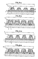
- a matrix of photosensitive elements can be produced by following the method described below with reference to FIGS. 5a and 5b for a first variant, or to FIGS. 6a and 6b for a second variant.
- Figures 5a and 6a show the matrix in section along a column
- Figures 5b and 6b show the matrix in section along a line respectively for the two variants of the method.
- this matrix is produced from amorphous silicon in the following manner: a glass plate 1 forming the substrate is covered in a first phase with a layer of semi-transparent conductor 2, for example molybdenum, tantalum or ITO (mixture of indium oxide and tin oxide), which is then etched to form the column conductors.
- a layer of dielectric material 3 is then formed, for example of tantalum oxide Ta 2 0 5 of high dielectric constant under a thickness of 0.2 ⁇ m obtained by anodic oxidation of the preceding layer if the latter is produced in tantalum, for forming the capacitances C.
- amorphous silicon intended to form the PIN diodes, D under a thickness of the order of 0.8 ⁇ m to 3 / lm: for example a layer of silicon doped p +, 4, an intrinsic silicon layer i, 5, and an n + doped silicon layer, 6.
- the etching of these superposed layers then makes it possible to isolate the diodes superimposed on the dielectric layer forming the capacitors and in contact with the lower conductor.
- a semi-transparent metal layer 8, ITO for example is deposited; this layer is then etched to form the line conductors.
- the scintillator screen 9 can then be deposited on the assembly, the X image being projected onto this face of the matrix.
- the leveling optical flashes are projected on the side of the glass plate 1, the scintillator being opaque to visible radiation.
- the diodes are produced before the capacitors, the capacitors being formed from the insulating layer 7 , which prevents the opening of contacts in this layer, and prevents the deposition of the insulating layer 3.
- the layer 7 can obviously no longer be produced by oxidation of the lower semi-transparent conductor (tantalum).
- the succession of layers is then as follows: on the glass plate 1 is deposited a semi-transparent conductive material 2 which is then etched, then the silicon layers 4 p + doped, 5 intrinsic, and 6 n + doped. After etching to isolate the diodes, the layer of dielectric material 7 is deposited and constitutes the capacitances C. The last layer 8 of semi-transparent conductor is then deposited and then etched.
- stage 1 is that which corresponds to the load of the capacity column C c , at the low level of Vco, close to OV.
- the noise of stage 2 is that of stage 1 to which is added the noise for reading the diode. It is possible to completely get rid of the noise of level 1 which has spatial (variations from one column to another) and temporal components, by using for the reading of the output voltage of the integrator a double method sample swimming which consists in memorizing the signal of stage 1 on a capacity and in reading only the variation of signal from stage 1 to stage 3.
- the noise of level 3 depends on the input noise voltage of the amplifier, of its passband B, linked to the reading time allocated to each column. Multiplexing, made possible by the method of coincidence of voltage pulses Vp and Vco applied respectively to the rows and to the columns, described above makes it possible to reduce the bandwidth B and therefore to reduce the noise voltage accordingly by a factor ⁇ M, M being the rate of multiplexing.
- the registers can be produced with transistors of reduced mobility, as is the case for a photosensitive matrix using a material of the amorphous silicon type.
- FIGS. 7 The explanatory signals of the variant of the reading method implementing such a leveling are shown in FIGS. 7 in the case of an application where the leveling is carried out in one go for the entire matrix.
- the reference letters of Figures 7 and following are identical to those of Figures 3 and following for the same signals.
- the structure of the pulses Vp is modified as shown on the curve of FIG. 7b: the negative pulse necessary for the discharge for an electrical leveling up is suppressed; it is replaced by the calibrated illumination represented in FIG.
- the diodes of this same line cannot be read by the coincidences Vp and Vco intended for the reading of the following lines, it is important to choose the polarization charge background Q o greater than the maximum signal charge Qs (max) so that the potential of points A, after reading, (VA-Vp) T L is always greater than V AO . It is only after a new leveling that the discharge leads to the potential of the floating points V A suitable for reading.
- the exposure to useful radiation can take place after the upgrade, as previously, but can also be done before the upgrade, or even at the same time; which may be the case for a permanent image arrival, in the case of a visible imager. Integration on each line then takes place during the reading of all the other lines, but between each reading of the whole matrix must take place the sequence of leveling.
- the refresher can also be obtained by means of intense lighting.
- the explanatory signals of the variant of the reading method implementing such a leveling are represented in FIGS. 8a to 8h also in the case of an application where the leveling is carried out for the entire panel at one time.
- the intense, uncalibrated illumination, illustrated by FIG. 8h discharges the capacitance C much more than would be necessary to return to the starting voltage V AO .
- a blank reading is carried out by means of an additional reading pulse represented in FIG. 8b, of calibrated level Vpo, lower than V P1 , similar to that introduced after a strongly reverse polarization as in FIG. 3b.
- the application of this matrix to the taking of radiological images is an application in which there is only one exposure and only one reading of the matrix.
- the leveling operation is carried out for the entire matrix, prior to an exposure as indicated above. Reading can then be carried out line by line by electronic addressing.
- the invention is not limited to the description precisely given above, but in all cases, the necessary leveling for the read operation to be carried out correctly, whatever the level of the analog signal to be read by the integrating operational amplifier must be adapted to the application envisaged.
Abstract
L'invention a pour objet une matrice d'éléments photosensibles, dans laquelle chaque élément photosensible se réduit à l'association d'une diode (D) et d'une capacité (C). Son procédé de fabrication est donc facile notamment à partir de silicium amorphe. Son procédé de lecture met en oeuvre une lecture multiplexée des colonnes : les n colonnes sont réparties en groupe de ? colonnes successives commandés simultanément par M registres à décalage horizontaux (RH1,...RHM), chacun associé à un intégrateur de lecture (A1,...AM). Pour assurer une lecture correcte des signaux utiles, quel que soit leur niveau, une remise à niveau de la tension (VP-VA) aux bornes des diodes des éléments photosensibles est effectuée afin que la tension de départ (VA0) au début de chaque impulsion de lecture appliqué à une ligne soit telle que seule, et même avec un signal d'éclairement utile maximum, cette impulsion ne puisse polariser la diode en direct, et que avec une impulsion d'adressage de colonne, la diode soit polarisée en direct même en l'absence de signal utile. Application, notamment, à la prise de vue d'images radiologiques.The subject of the invention is a matrix of photosensitive elements, in which each photosensitive element is reduced to the association of a diode (D) and of a capacitor (C). Its manufacturing process is therefore easy, in particular from amorphous silicon. Its reading method implements a multiplexed reading of the columns: the n columns are distributed in groups of? successive columns controlled simultaneously by M horizontal shift registers (RH1, ... RHM), each associated with a read integrator (A1, ... AM). To ensure correct reading of the useful signals, whatever their level, a resetting of the voltage (VP-VA) at the terminals of the diodes of the photosensitive elements is carried out so that the starting voltage (VA0) at the start of each pulse of reading applied to a line is such that only, and even with a maximum useful illumination signal, this pulse cannot polarize the diode in direct, and that with a column addressing pulse, the diode is polarized in direct even in the absence of a useful signal. Application, in particular, to the taking of radiological images.
Description
L'invention se rapporte aux techniques d'imagerie et plus particulièrement à la prise de vue, notamment pour images radiologiques, au moyen de matrices d'éléments photosensibles.The invention relates to imaging techniques and more particularly to shooting, in particular for radiological images, by means of arrays of photosensitive elements.
La réalisation d'une matrice d'éléments photosensibles de grande dimension se heurte à de nombreuses difficultés tant au niveau de la structure des éléments photosensibles, qui doit être aussi simple que possible pour des raisons de rendement de fabrication, qu'au niveau de l'utilisation de cette matrice, la lecture des éléments photosensibles devant, pour être efficace, être rapide et à faible bruit.The production of a matrix of large photosensitive elements faces many difficulties both at the level of the structure of the photosensitive elements, which must be as simple as possible for reasons of manufacturing efficiency, and at the level of the 'use of this matrix, reading photosensitive elements before, to be effective, be fast and low noise.
Un premier objet de la présente invention est une matrice d'élements photosensibles interconnectés dans laquelle chaque élément se limite à l'association d'une photodiode et d'une capacité. L'avantage d'un tel élément photosensible est d'être dépourvu d'élément de commutation ; il présente donc un rendement de fabrication potentiel élevé. Par contre sa lecture nécessite l'emploi d'un amplificateur opérationnel intégrateur, et requiert un temps relativement long pour être efficace et à faible bruit. Selon l'invention une matrice d'éléments photosensibles comportant un ensemble de p lignes de n éléments photosensibles, chaque élément ayant une première et une seconde borne, est caractérisée en ce que chaque élément comporte en série une photodiode et une capacité, les premières bornes des éléments d'une même ligne étant interconnectées et reliées via un interrupteur commandé par une sortie d'un registre à décalage vertical à un potentiel d'adressage ligne, et les secondes bornes des éléments d'une même colonne étant interconnectées et reliées à un interrupteur, commandé par une sortie de l'un de M registres à décalage horizontaux à étages, en série avec l'entrée "-" de l'un des M amplificateurs opérationnels montés en intégrateur, les entrées "+" des intégrateurs étant reliées à l'entrée d'adressage colonne, chaque conducteur de colonne étant également relié, via un interrupteur commandé par des impulsions de remise à niveau à l'entrée d'adressage colonne, les entrées de commande de décalage des registres horizontaux étant reliées à une même entrée de commande, chaque intégrateur comportant des moyens de remise à zéro de la capacité d'intégration.A first object of the present invention is a matrix of interconnected photosensitive elements in which each element is limited to the association of a photodiode and a capacitance. The advantage of such a photosensitive element is that it does not have a switching element; it therefore has a high potential manufacturing yield. On the other hand, reading it requires the use of an integrating operational amplifier, and requires a relatively long time to be efficient and low noise. According to the invention, a matrix of photosensitive elements comprising a set of p lines of n photosensitive elements, each element having a first and a second terminal, is characterized in that each element comprises in series a photodiode and a capacitance, the first terminals elements of the same line being interconnected and connected via a switch controlled by an output of a vertical shift register to a line addressing potential, and the second terminals of the elements of the same column being interconnected and connected to a switch, controlled by an output of one of M horizontal shift registers with stages, in series with the input "-" of one of the M operational amplifiers mounted as an integrator, the inputs "+" of the integrators being connected to the column addressing input, each column conductor also being connected, via a switch controlled by leveling pulses to the column addressing input, the control inputs d e offset of the horizontal registers being connected to the same control input, each integrator comprising means for resetting the integration capacity to zero.
Un second objet de l'invention est le procédé de fabrication de cette matrice.A second object of the invention is the method of manufacturing this matrix.
Selon l'invention un procédé de fabrication d'une matrice d'éléments photosensibles, est caractérisé en ce qu'il consiste :
- - à déposer sur un substrat transparent une première couche de matériau conducteur semi-transparent et à la graver pour obtenir des conducteurs parallèles,
- - à déposer sur cet ensemble des couches successives de matériau semi-conducteur, respectivement dopée, non dopée et dopée nécessaires pour former des diodes photosensibles, puis à les graver pour isoler des diodes,
- - à recouvrir cet ensemble d'une couche de matériau diélectrique pour réaliser des capacités, en série avec les diodes,
- - puis, à déposer une couche de matériau conducteur semi-transparent sur la couche diélectrique, et à la graver pour réaliser des conducteurs de colonne orthogonaux aux conducteurs de ligne et reliant les capacités d'une même ligne.
- - depositing on a transparent substrate a first layer of semi-transparent conductive material and etching it to obtain parallel conductors,
- to deposit on this assembly successive layers of semiconductor material, respectively doped, undoped and doped necessary to form photosensitive diodes, then to etch them to isolate diodes,
- to cover this assembly with a layer of dielectric material to make capacitors, in series with the diodes,
- - Then, to deposit a layer of semi-transparent conductive material on the dielectric layer, and to etch it to produce column conductors orthogonal to the line conductors and connecting the capacities of the same line.
Un autre objet de l'invention est le procédé de lecture associé à cette matrice d'éléments photosensibles. Il effectue un multiplexage des colonnes de la matrice, de façon que les amplificateurs intégrateurs fonctionnent dans des conditions satisfaisantes, sans en multiplier trop le nombre.Another object of the invention is the reading method associated with this matrix of photosensitive elements. It performs a multiplexing of the columns of the matrix, so that the integrating amplifiers operate under satisfactory conditions, without multiplying the number too much.
Selon l'invention, le procédé de lecture associé à la matrice telle que décrite ci-dessus est caractérisé
- - en ce que pour la lecture, les registres à décalage horizontaux sont commandés en parallèle, la lecture des colonnes étant multiplexée : les éléments photosensibles d'une ligne sont adressés par une tension d'adressage appliquée simultanément aux colonnes de rangs k, k +


- - et en ce qu'une phase de remise à niveau des tensions aux bornes des diodes est prévue, par application d'un fond de charge aux éléments photosensibles, entre les séquences de lecture, pour ramener la tension aux bornes des diodes d'une ligne à lire à une valeur initiale VAO telle que les impulsions de lecture ligne seules ne puissent les polariser en direct même après un éclairement maximum, et que les impulsions de commande ligne associées aux impulsions d'adressage colonne les polarise fortement en direct, même en l'absence de rayonnement utile.
- - in that for reading, the horizontal shift registers are controlled in parallel, the reading of the columns being multiplexed: the photosensitive elements of a line are addressed by an addressing voltage applied simultaneously to the columns of rows k, k +
- - And in that a phase for updating the voltages across the diodes is provided, by applying a charge background to the photosensitive elements, between the reading sequences, to bring the voltage across the diodes of a line to be read at an initial value V AO such that the line read pulses alone cannot polarize them directly even after maximum illumination, and that the line command pulses associated with the column addressing pulses strongly polarize them even in the absence of useful radiation.
Le dernier objet de l'invention est l'application de cette matrice à la prise de vue d'images, notamment radiologiques.The last object of the invention is the application of this matrix to the taking of images, in particular radiological images.
L'invention sera mieux comprise et d'autres caractéristiques apparaîtront à l'aide de la description qui suit en référence aux figures annexées.The invention will be better understood and other characteristics will appear from the following description with reference to the appended figures.
- La figure 1 représente une matrice d'éléments photosensibles selon l'invention, et les moyens de lecture associés ;FIG. 1 represents a matrix of photosensitive elements according to the invention, and the associated reading means;
- La figure 2 est un schéma de détail d'un élément photosensible et des moyens de lecture associés ;FIG. 2 is a detailed diagram of a photosensitive element and of the associated reading means;
- Les figures 3a à 3h représentent des signaux explicatifs du fonctionnement de la matrice selon l'invention avec une première variante de procédé de lecture;FIGS. 3a to 3h represent signals explaining the operation of the matrix according to the invention with a first variant of the reading method;
- La figure 4 est un schéma de détails de l'un des signaux décrits en référence à la figure 3 ;Figure 4 is a detailed diagram of one of the signals described with reference to Figure 3;
- Les figures 5a et 5b représentent des vues en coupe, respectivement selon une colonne et selon une ligne, d'une matrice obtenue selon une première variante de procédé de fabrication ;Figures 5a and 5b show views in cutting, respectively along a column and along a line, of a matrix obtained according to a first variant of the manufacturing process;
- Les figures 6a et 6b représentent des vues en coupe, respectivement selon une colonne et selon une ligne, d'une matrice obtenue selon une seconde variante de procédé de fabrication.Figures 6a and 6b show sectional views, respectively along a column and along a line, of a matrix obtained according to a second variant of the manufacturing process.
- Les figures 7a, 7b...7h représentent des signaux explicatifs du fonctionnement de la matrice avec une seconde variante du procédé de lecture ;Figures 7a, 7b ... 7h represent explanatory signals for the operation of the matrix with a second variant of the reading method;
- Les figures 8a, 8b...8h représentent des signaux explicatifs du fonctionnement de la matrice avec une troisième variante du procédé de lecture.Figures 8a, 8b ... 8h show explanatory signals for the operation of the matrix with a third variant of the reading method.
Sur la figure 1 qui représente une vue d'ensemble de la matrice photosensible, un nombre n.p éléments photosensibles, chacun constitué d'une photodiode D en série avec une capacité C, sont arrangés suivant les lignes et les colonnes d'une matrice de p lignes et n colonnes, les diodes d'une même ligne sont reliées entre elles par une connexion de ligne, tandis que les capacités C d'une même colonne sont reliées entre elles par une connexion de colonne. Les connexions de lignes sont reliées à une tension d'adressage Vp par l'intermédiaire de transistors MOS interrupteurs, ji, j2...jp commandés par les sorties vi, v2...vp d'un registre à décalage dit registre à décalage vertical, RV. Ce registre est commandé par un signal de commande CDV de décalage vertical. Ainsi, lorsqu'une ligne est sélectionnée pour être lue, toutes les diodes de cette ligne sont portées au niveau haut VP1 du potentiel d'adressage Vp. De la même manière, les capacités d'une même colonne sont reliées aux entrées d'amplificateurs opérationnels montés en intégrateurs, par l'intermédiaire de transistors MOS interrupteurs i1, i2..., in commandés par les sorties des étages de registres à décalage horizontaux.In Figure 1 which shows an overview of the photosensitive matrix, a number np photosensitive elements, each consisting of a photodiode D in series with a capacitance C, are arranged along the lines and columns of a matrix of p rows and n columns, the diodes of the same line are connected to each other by a line connection, while the capacitances C of the same column are connected to each other by a column connection. The line connections are connected to an addressing voltage Vp by means of MOS switch transistors, j i , j 2 ... jp controlled by the outputs vi, v 2 ... vp of a so-called shift register vertical shift register, RV. This register is controlled by a control signal C DV of vertical shift. Thus, when a line is selected to be read, all the diodes of this line are brought to the high level V P1 of the addressing potential Vp. In the same way, the capacities of the same column are connected to the inputs of operational amplifiers mounted as integrators, by means of MOS switch transistors i 1 , i 2 ..., i n controlled by the outputs of the stages of horizontal shift registers.
Selon l'invention, le procédé de lecture réalise un multiplexage des colonnes de la matrice, pour ne pas utiliser un amplificateur intégrateur par colonne : plusieurs colonnes successives sont reliées à l'entrée d'un même amplificateur opérationnel intégrateur. Les moyens de lecture comportent donc M amplificateurs, M étant un diviseur de n, et M registres à décalage horizontaux, chaque amplificateur et le registre à décalage horizontal associé étant utilisés pour la lecture de ![]()
![]()
![]()
![]()
![]()
![]()
Cette structure est répétée pour chaque paquet de ![]()
![]()
![]()
![]()
La figure 2 représente en détails le schéma équivalent d'un élément photosensible à photodiode D et capacité C, avec les différentes commandes d'adressage et l'amplificateur de sortie correspondant. Lorsque cet élément photosensible est sélectionné par le registre vertical Rvde la figure 1, l'interrupteur j correspondant est fermé par la commande v et le potentiel Vp est appliqué sur la diode D. La capacité CD de la diode a été représentée en parallèle sur cette diode D. Le point commun à la diode D et la capacité C a été désigné par A, l'autre extrémité de la capacité C étant reliée à l'entrée "-" de l'amplificateur opérationnel intégrateur G par l'intermédiaire du transistor MOS interrupteur i commandé par la sortie h d'un registre à décalage horizontal de sélection de la colonne. Entre cette même borne de C et la masse a été représentée la capacité de la connexion de colonnes Cc.FIG. 2 shows in detail the equivalent diagram of a photosensitive element with photodiode D and capacitance C, with the different addressing commands and the corresponding output amplifier. When this photosensitive element is selected by the vertical register Rv in FIG. 1, the corresponding switch j is closed by the command v and the potential Vp is applied to the diode D. The capacitance C D of the diode has been represented in parallel on this diode D. The point common to the diode D and the capacitance C has been designated by A, the other end of the capacitance C being connected to the input "-" of the integrating operational amplifier G via the MOS transistor switch i controlled by the output h of a column shift horizontal register. Between this same terminal of C and ground has been represented the capacity of the connection of columns C c .
Les diagrammes des figures 3a à 3h représentent les différents signaux appliqués ou obtenus lors de la lecture d'un élément photosensible.The diagrams in FIGS. 3a to 3h represent the different signals applied or obtained during the reading of a photosensitive element.
Si l'on considère les opérations de lecture de la ième ligne, toutes les diodes de cette ligne ont été polarisées en inverse par la précédente lecture de cette même ligne, une durée Ti auparavant, cette durée étant au minimum la durée nécessaire pour la lecture de toutes les autres lignes. Les points A communs entre diode D et capacité C des éléments photosensibles de cette ligne sont alors polarisés positivement, et laissés flottants pendant toute la durée T;, cette durée étant également mise à profit pour l'intégration de l'information lumineuse à enregistrer par cette ligne. Le photocourant propre à chaque diode abaisse plus ou moins le potentiel de chaque point A par la décharge de chaque couple capacitif formé par la capacité C et la capacité de la diode CD, comme le montre la figure 3f représentant la tension aux bornes d'une diode, où les traits pleins et pointillés représentent respectivement le cas où il n'y a pas de signal lumineux utile et le cas où il y a un signal lumineux utile. Co est supposée petite devant C, c'est-à-dire CD est inférieure ou égale à C 10.If we consider the read operations of the ith line, all the diodes of this line have been reverse biased by the previous reading of this same line, a duration Ti previously, this duration being at least the duration necessary for reading of all the other lines. The points A common between diode D and capacitance C of the photosensitive elements of this line are then positively polarized, and left floating throughout the duration T ;, this duration also being used for the integration of the light information to be recorded by this line. The photocurrent specific to each diode more or less lowers the potential of each point A by the discharge of each capacitive couple formed by the capacitance C and the capacitance of the diode C D , as shown in FIG. 3f representing the voltage across the terminals of a diode, where the solid and dotted lines represent respectively the case where there is no useful light signal and the case where there is a useful light signal. Co is assumed to be small in front of C, i.e. C D is less than or equal to C 10.
Les opérations de lecture de la ligne se décomposent en deux séquences successives :
- - tout d'abord la lecture séquentielle des informations stockées sur les points A des différents groupes de éléments photosensibles, les M groupes de colonnes étant lus simultanément grâce aux M registres à décalages horizontaux et aux M amplificateurs intégrateurs ;
- - dans une seconde phase, la restauration simultanée du potentiel initial VAO des points A de toute la ligne, par une remise à niveau, soit au moyen d'une impulsion de polarisation négative appliquée à cette ligne suivie d'une lecture à blanc, soit au moyen d'un éclairement uniforme calibré appliqué sélectivement à la ligne de photodétecteurs, soit au moyen d'un flash lumineux intense suivi d'une lecture à blanc.
- - firstly the sequential reading of the information stored on the points A of the different groups of photosensitive elements, the M groups of columns being read simultaneously thanks to the M registers with horizontal shifts and to the M integrating amplifiers;
- - in a second phase, the simultaneous restoration born from the initial potential V AO of points A of the whole line, by a leveling, either by means of a negative bias pulse applied to this line followed by a blank reading, or by means of a uniform illumination calibrated selectively applied to the line of photodetectors, either by means of an intense luminous flash followed by a blank reading.
Ces deux opérations s'effectuent grâce à l'aiguillage de la tension d'adressage Vp sur la iéme ligne par le registre à décalage vertical Rv qui commande la fermeture de l'interrupteur ji correspondant à cette ligne : la tension appliquée à la ligne, Vp est nulle pendant toute la durée T; et égale au niveau haut de Vp, VP1 pendant la durée des impulsions de lecture TL comme le montre la figure 3b. La première séquence est une suite de n M impulsions de lecture, synchrones des impulsions de remise à zéro VRAZ court circuitant les condensateurs de lecture CL et des impulsions d'adressage Vco.h appliquées aux entrées positives des M amplificateurs, comme représenté sur les figures 3c où a été représenté Vco et VRAZ, 3d et 3e où ont été représentés les produits logigues Vco.h1 et Vco.h2, correspondant à l'adressage des deux premières colonnes de chaque groupe. Ces impulsions d'adressage colonne, Vco.h résultent de la combinaison logique d'impulsions h commandant les interrupteurs i et d'impulsions appliquées au point de potentiel de référence des colonnes Vco. Les impulsions h encadrent les impulsions Vco de façon que, à la fin d'une durée de lecture TL, la tension de colonne soit bien ramenée au niveau haut de Vco avant la remise à niveau. Les impulsions d'adressage colonne et de remise à zéro débordent de chaque côté des impulsions de lecture Vp : les impulsions Vp passent au niveau haut VP1 après que les impulsions Vco soient passées au niveau bas. Les impulsions de lecture ne sont donc transmises que sur les colonnes sélectionnées par les registres à décalage horizontaux, les autres colonnes restent chargées, au niveau haut de Vco.These two operations are carried out by switching the addressing voltage Vp on the ith line by the vertical shift register R v which controls the closing of the switch j i corresponding to this line: the voltage applied to the line, Vp is zero during the whole duration T; and equal to the high level of Vp, V P1 during the duration of the read pulses T L as shown in FIG. 3b. The first sequence is a sequence of n M read pulses, synchronous of the reset pulses V RESET short circuiting the read capacitors C L and of the addressing pulses Vco.h applied to the positive inputs of the M amplifiers, as shown in FIGS. 3c where Vco and V Reset have been represented, 3d and 3e where the log products Vco.h 1 and Vco.h 2 have been represented, corresponding to the addressing of the first two columns of each group. These column addressing pulses, Vco.h result from the logical combination of pulses h controlling the switches i and pulses applied to the reference potential point of the columns Vco. The pulses h surround the pulses Vco so that, at the end of a reading time T L , the column voltage is indeed brought back to the high level of Vco before the resetting. The column addressing and reset pulses overflow on each side of the reading pulses Vp: the pulses Vp pass to the high level VP1 after the pulses Vco have gone to the low level. The read pulses are therefore only transmitted on the columns selected by the horizontal shift registers, the other columns remain loaded, at the high level of Vco.
La figure 3f décrit l'évolution du potentiel VA-Vp aux bornes des diodes des colonnes 2, n M +2, 2 n M +2... Pendant l'adressage des colonnes précédentes 1, n M + 1, 2 n M +1 ..., les autres colonnes demeurant au niveau haut, l'impulsion sur Vp doit être d'amplitude VP1 insuffisante pour polariser leurs diodes en direct, en l'absence de rayonnement utile, Vaso ≧ 0, et également en présence de rayonnement VAS ≧ 0. C'est ce qui apparaît sur la figure 3f où a été représentée, en plus de la tension VA-Vpen fonction du temps, la caractéristique de la diode : ID courant dans la diode en fonction de VA-VP tension à ses bornes. Comme indiqué ci-dessus, le tracé en trait plein représente le potentiel en l'absence d'éclairement, le tracé en pointillés représente le potentiel d'une diode ayant intégrée une information lumineuse Qs pendant la période d'intégration Ti. AVA représente l'amplitude du signal stocké sur la capacité C, les charges Qs étant égales à C.AVA.FIG. 3f describes the evolution of the potential VA-V p at the terminals of the diodes of
L'amplitude de la variation de la tension aux bornes de la diode lors du passage de Vp au niveau haut VP1 est voisine de la variation d'amplitude de VP. La lecture des M colonnes suivantes, 2, n M +2... s'effectue par la coïncidence d'une impulsion Vp avec la tension d'adressage correspondante représentée par le produit logique Vco.h2 sur ces colonnes. Dans ce cas l'amplitude de la variation de la tension aux bornes de la diode doit être suffisante pour polariser la diode largement en direct, même en l'absence de signal lumineux utile, au niveau VASO - VP1. et bien entendu en présence de signal VAS - VP1. Si cette condition est réalisée, la tension aux bornes de la diode évolue pendant le temps de lecture TL jusqu'à une valeur Vc indépendante de la tension de polarisation initiale et donc du signal. Cette tension est la tension de coude de la diode D. Dans ce cas la charge signal se trouve intégralement transmise à la capacité CL de l'amplificateur intégrateur correspondant, quelle que soit son amplitude. Elle se trouve additionnée à une charge Qo qui est la charge lue en l'absence de signal. L'intégrateur G1, CL1 délivre alors en sortie une tension VS1 en présence de signal lumineux sur la colonne 2 qui correspond à la charge utile Qs et à
. Cette tension est disponible directement après le retour à zéro de la tension Vp et peut alors être prélevée par un échantillonneur avant le retour à zéro par VRAz. Les signaux Vco et VRAZ sont en phase mais peuvent avoir des niveaux différents.. This voltage is available directly after the return to zero of the voltage Vp and can then be taken by a sampler before the return to zero by V RA z. The Vco and V RESET signals are in phase but can have different levels.
Lors du retour de h2.Vco au niveau haut, la diode D se trouve plus fortement polarisée en inverse qu'initialement du fait de la lecture de la charge Qo + Qs. Le potentiel du point A s'écrit en effet
Pendant la lecture de toutes les autres colonnes, la diode reste polarisée en inverse sans être affectée par les variations de potentiel de Vp.During the reading of all the other columns, the diode remains reverse biased without being affected by the variations in potential of Vp.
Au terme des - impulsions de Vp, la séquence de lecture des colonnes est achevée pour la ligne i. La phase de remise à niveau de tous les points flottants A des diodes de cette ligne est alors effectuée. Le but de cette remise à niveau est de restaurer sur les diodes un potentiel VAotel que les impulsions de Vp ne puisse les polariser en direct lors d'une lecture même pour un éclairement maximum, et en même temps que la somme des amplitudes de Vp et de Vco les polarise fortement en direct même en l'absence de signal. Cette double condition permet de sélectionner la lecture de chaque diode par la coïncidence des impulsions de commande de ligne, par Vp, et des impulsions de commande de colonne par Vco selon la description ci-dessus.At the end of the pulses of Vp, the reading sequence of the columns is completed for the line i. The phase of updating all the floating points A of the diodes of this line is then carried out. The purpose of this upgrade is to restore a potential V A otel on the diodes that the pulses of Vp cannot polarize them directly during a reading even for maximum illumination, and at the same time as the sum of the amplitudes of Vp and de Vco polarize them strongly in direct even in the absence of signal. This double condition makes it possible to select the reading of each diode by the coincidence of the line control pulses, by Vp, and the column control pulses by Vco according to the description above.
Pour obtenir le potentiel VAO nécessaire, il faut tout d'abord décharger le couple de capacités C et CD, que l'opération de lecture précédente a rechargé à une tension supérieure àVAo où la diode ne peut plus être lue convenablement. Plusieurs méthodes sont possibles pour effectuer cette décharge : soit l'utilisation de la conduction en inverse de la diode au delà d'un certain seuil, soit un éclairement intense ou uniforme selon les applications envisagées.To obtain the necessary potential V AO , it is first necessary to discharge the pair of capacitors C and C D , which the previous reading operation has recharged at a voltage greater than V A o where the diode can no longer be read properly. Several methods are possible to perform this die load: either the use of the reverse conduction of the diode beyond a certain threshold, or an intense or uniform illumination according to the envisaged applications.
En utilisant le seuil de conduction en inverse de la diode, l'opération de remise à niveau illustrée par les diagrammes de signaux des figures 3a et suivantes consiste à appliquer une impulsion négative d'amplitude VP2 par Vp qui polarise la diode au delà de son seuil de conduction en inverse. Celle-ci se décharge jusqu'à la tension de coude inverse VCI, indépendante de la tension initiale. Pendant cette opération ainsi que pendant la suivante, toutes les colonnes sont polarisées au niveau haut de Vco par l'intermédiaire des transistors interrupteurs MOS i"1...i"ncommandés pour la remise à niveau par VRAN. Cette opération de polarisation au delà du seuil de conduction en inverse est suivie par une séquence de lecture "à blanc" au terme de laquelle le potentiel final VAσpeut être ajusté au moyen d'une impulsion de lecture d'amplitude déterminée Vpo. Ainsi la charge de polarisation Qo est ajustée indépendamment de la valeur de tension de coude inverse de la diode, qui peut varier sensiblement d'un élement à l'autre, pour que Vc + Vpo + Vco = VAO. Au terme de cette séquence le potentiel flottant de toutes les diodes de la ième ligne est restauré pour commencer une nouvelle intégration de l'information lumineuse.Using the reverse conduction threshold of the diode, the resetting operation illustrated by the signal diagrams of FIGS. 3a and following consists in applying a negative pulse of amplitude V P2 by Vp which polarizes the diode beyond its inverse conduction threshold. This discharges up to the reverse elbow tension VCI, independent of the initial tension. During this operation as well as during the following one, all the columns are biased at the high level of Vco by means of the MOS switch transistors i " 1 ... i" n controlled for updating by V RAN . This polarization operation beyond the inverse conduction threshold is followed by a "blank" reading sequence at the end of which the final potential V A σ can be adjusted by means of a reading pulse of determined amplitude Vpo. Thus the polarization charge Qo is adjusted independently of the value of the reverse elbow voltage of the diode, which can vary appreciably from one element to another, so that Vc + Vpo + Vco = V AO . At the end of this sequence the floating potential of all the diodes of the ith line is restored to begin a new integration of the light information.
Une matrice d'éléments photosensibles, telle que décrite ci-dessus et représentée schématiquement sur la figure 1 peut être réalisée en suivant le procédé décrit ci-dessous en référence aux figures 5a et 5b pour une première variante, ou aux figures 6a et 6b pour une seconde variante. Les figures 5a et 6a représentent la matrice en coupe suivant une colonne, et les figures 5b et 6b représentent la matrice en coupe suivant une ligne respectivement pour les deux variantes du procédé.A matrix of photosensitive elements, as described above and shown diagrammatically in FIG. 1, can be produced by following the method described below with reference to FIGS. 5a and 5b for a first variant, or to FIGS. 6a and 6b for a second variant. Figures 5a and 6a show the matrix in section along a column, and Figures 5b and 6b show the matrix in section along a line respectively for the two variants of the method.
Selon la première variante cette matrice est réalisée à partir de silicium amorphe de la manière suivante : une plaque de verre 1 formant le substrat est recouverte dans une première phase d'une couche de conducteur semi-transparent 2, par exemple du molybdène, du tantale ou de l'ITO (mélange d'oxyde d'indium et d'oxyde d'étain), qui est ensuite gravée pour former les conducteurs de colonnes. Une couche de matériau diélectrique 3 est alors formée, par exemple de l'oxyde de tantale Ta2 05 de forte constante diélectrique sous une épaisseur de 0.2 p.m obtenue par oxydation anodique de la couche précédente si celle-ci est réalisée en tantale, pour former les capacités C. Puis sont déposées sur cette couche les couches de silicium amorphe destinées à former les diodes PIN, D sous une épaisseur de l'ordre de 0.8 µm à 3 /lm: par exemple une couche de silicium dopée p+, 4, une couche de silicium intrinsèque i, 5, et une couche de silicium dopée n+, 6. La gravure de ces couches superposées permet alors d'isoler les diodes superposées à la couche diélectrique formant les condensateurs et en contact avec le conducteur inférieur. Une couche de protection isolante 7, formée de nitrure ou d'oxyde de silicium par exemple, est alors déposée ; enfin des contacts sont ouverts dans la couche superficielle d'isolant 7 pour réaliser les conducteurs de ligne. Pour cela une couche de métal semi-transparent 8, ITO par exemple, est déposée ; cette couche est ensuite gravée pour former les conducteurs de ligne.According to the first variant, this matrix is produced from amorphous silicon in the following manner: a
Pour une application à l'imagerie X l'écran scintillateur 9 peut alors être déposé sur l'ensemble, l'image X étant projetée sur cette face de la matrice. Dans le cas où la remise à niveau est effectuée par éclairement comme il sera expliqué ci-après, les flash optiques de remise à niveau sont projetés du côté de la plaque de verre 1, le scintillateur étant opaque au rayonnement visible.For an application to X imaging, the
Selon la deuxième variante, illustrée par les figures 6a et 6b, où les mêmes couches que sur les figures 5a et 5b portent les mêmes références, les diodes sont réalisées avant les capacités, les capacités étant formées à partir de la couche d'isolant 7, ce qui évite l'ouverture de contacts dans cette couche, et évite le dépôt de la couche d'isolant 3. La couche 7 ne peut évidemment plus être réalisée par oxudation du conducteur semi-transparent inférieur (tantale). La succession des couches est alors la suivante : sur la plaque de verre 1 est déposé un matériau conducteur semi-transparent 2 qui est ensuite gravé, puis les couches de silicium 4 dopée p+, 5 intrinsèque, et 6 dopée n+. Après gravure pour isoler les diodes la couche de matériau diélectrique 7 est déposée et constitue les capacité C. La dernière couche 8 de conducteur semi-transparent est alors déposée puis gravée.According to the second variant, illustrated by FIGS. 6a and 6b, where the same layers as in FIGS. 5a and 5b bear the same references, the diodes are produced before the capacitors, the capacitors being formed from the insulating
On réalise ainsi facilement des matrices de points dans lesquelles chaque zone élémentaire a un côté de l'ordre de 100 µm à 200 µm, et donc des matrices de 2000 x 2000 points à 4000 x 4000 points dont les dimensions sont de l'ordre de 40 cm x 40 cm.It is thus easy to produce point matrices in which each elementary zone has a side of the order of 100 μm to 200 μm, and therefore matrices of 2000 × 2000 points to 4000 × 4000 points whose dimensions are of the order of 40 cm x 40 cm.
La structure ainsi obtenue pour la matrice et le procédé de lecture associé présentent plusieurs avantages dans le cas d'un photosen seur matriciel de grande dimension pour lequel on souhaite obtenir une résolution élevée :
- - le bruit de lecture peut être réduit au minimum ;
- - la fréquence de fonctionnement des registres à décalage horizontaux peut également être réduite par le facteur M du fait du multiplexage ;
- - l'élément photosensible qui est une association capacité et diode a une structure très simple, résistante au rayonnement X, ce qui est un avantage capital pour un senseur destiné à l'imagerie par rayonnement X, employé par exemple avec un scintillateur.
- - reading noise can be reduced to a minimum;
- - the operating frequency of the horizontal shift registers can also be reduced by the factor M due to multiplexing;
- - The photosensitive element which is a combination of capacitance and diode has a very simple structure, resistant to X-radiation, which is a capital advantage for a sensor intended for X-ray imaging, used for example with a scintillator.
En ce qui concerne la réduction du bruit de lecture, un détail de la tension de sortie est représenté sur la figure 4 où il est possible de distinguer les trois paliers avec les bruits correspondant. Le bruit du palier 1 est celui qui correspond à la charge de la colonne de capacité Cc, au niveau bas de Vco, proche de OV.With regard to the reduction of the reading noise, a detail of the output voltage is shown in FIG. 4 where it is possible to distinguish the three stages with the corresponding noises. The noise of
le bruit du palier 2 est celui du palier 1 auquel s'ajoute le bruit de lecture de la diode. Il est possible de s'affranchir complétement du bruit du palier 1 qui comporte des composantes spatiales (variations d'une colonne à l'autre) et temporelles, en employant pour la lecture de la tension de sortie de l'intégrateur une méthode de double échantillonnage qui consiste à mettre en mémoire le signal du palier 1 sur une capacité et à ne lire que la variation de signal du palier 1 au palier 3.the noise of
Le bruit du palier 3 dépend de la tension de bruit d'entrée de l'amplificateur, de sa bande passante B, liée au temps de lecture alloué à chaque colonne. Le multiplexage, rendu possible par le procédé de coïncidence d'impulsions de tension Vp et Vco respectivement appliquées aux lignes et aux colonnes, décrit ci-dessus permet de réduire la bande passante B et donc de réduire en conséquence la tension de bruit par un facteur √M, M étant le taux de multiplexage.The noise of
En ce qui concerne la fréquence de fonctionnement des registres à décalage horizontaux, du fait de sa réduction, les registres peuvent être réalisés avec des transistors de mobilité réduite, comme c'est le cas pour une matrice photosensible utilisant un matériau du type silicium amorphe.As regards the operating frequency of the horizontal shift registers, due to its reduction, the registers can be produced with transistors of reduced mobility, as is the case for a photosensitive matrix using a material of the amorphous silicon type.
Ce matériau est alors utilisé pour l'ensemble de la structure ce qui simplifie considérablement les problèmes de connexion.This material is then used for the entire structure, which considerably simplifies connection problems.
Il a été indiqué ci-dessus que l'opération de remise à niveau indispensable pour que la lecture puisse être répétée, pouvait être effectuée en éclairant uniformément les diodes de façon à les décharger, cet éclairement ayant une intensité et une durée prédéterminées. Les signaux explicatifs de la variante du procédé de lecture mettant en oeuvre une telle remise à niveau sont représentés sur les figures 7 dans le cas d'une application où la remise à niveau est effectuée en une seule fois pour toute la matrice. Les lettres références des figures 7 et suivantes sont identiques à celles des figures 3 et suivantes pour les mêmes signaux. La structure des impulsions Vp est modifiée comme représenté sur la courbe de la figure 7b : l'impulsion négative nécessaire à la décharge pour une remise à niveau électrique est supprimée ; elle est remplacée par l'éclairement calibré représenté sur la figure 7h qui décharge pendant un temps prédéterminé toutes les diodes de la matrice après la lecture de toutes les lignes de l'image précédente. C'est cette décharge qui fixe la tension de départ VAO ; l'impulsion de lecture à blanc d'amplitude Vpo est également supprimée. Les impulsions de lecture suivantes réalisent les lectures successives des diodes de la matrice, en coïncidence avec les impulsions Vco commandées par les registres horizontaux. Chaque diode qui vient d'être lue doit se trouver suffisamment polarisée en inverse pour ne plus être affectée par les autres impulsions de la séquence. Pour que les diodes de cette même ligne ne puissent être lues par les coïncidences Vp et Vco destinées à la lecture des lignes suivantes, il importe de choisir le fond de charge de polarisation Qo supérieur à la charge signal maximal Qs (max) pour que le potentiel des points A, après lecture, (VA-Vp)TLsoit toujours supérieur à VAO. Ce n'est qu'après une nouvelle remise à niveau que la décharge conduit au potentiel des points flottants VAoconvenable pour la lecture. Dans cette variante, contrairement aux autres, l'exposition au rayonnement utile peut avoir lieu après la remise à niveau, comme précédemment, mais peut également se faire avant la remise à niveau, ou même en même temps ; ce qui peut être le cas pour une arrivée permanente d'image, dans le cas d'un imageur visible. L'intégration sur chaque ligne a alors lieu pendant la lecture de toutes les autres lignes, mais entre chaque lecture de toute la matrice doit avoir lieu la séquence de remise à niveau.It was indicated above that the resetting operation essential for the reading to be repeated, could be carried out by uniformly illuminating the diodes so as to discharge them, this illumination having a predetermined intensity and duration. The explanatory signals of the variant of the reading method implementing such a leveling are shown in FIGS. 7 in the case of an application where the leveling is carried out in one go for the entire matrix. The reference letters of Figures 7 and following are identical to those of Figures 3 and following for the same signals. The structure of the pulses Vp is modified as shown on the curve of FIG. 7b: the negative pulse necessary for the discharge for an electrical leveling up is suppressed; it is replaced by the calibrated illumination represented in FIG. 7h which discharges for a predetermined time all the diodes of the matrix after the reading of all the lines of the previous image. It is this discharge which fixes the starting voltage V AO ; the blank reading pulse of amplitude Vpo is also suppressed. The following read pulses carry out the successive readings of the diodes of the matrix, in coincidence with the Vco pulses controlled by the horizontal registers. Each diode which has just been read must be sufficiently reverse biased to no longer be affected by the other pulses of the sequence. So that the diodes of this same line cannot be read by the coincidences Vp and Vco intended for the reading of the following lines, it is important to choose the polarization charge background Q o greater than the maximum signal charge Qs (max) so that the potential of points A, after reading, (VA-Vp) T L is always greater than V AO . It is only after a new leveling that the discharge leads to the potential of the floating points V A suitable for reading. In this variant, unlike the others, the exposure to useful radiation can take place after the upgrade, as previously, but can also be done before the upgrade, or even at the same time; which may be the case for a permanent image arrival, in the case of a visible imager. Integration on each line then takes place during the reading of all the other lines, but between each reading of the whole matrix must take place the sequence of leveling.
La remise à niveau peut également être obtenue au moyen d'un éclairement intense. Les signaux explicatifs de la variante du procédé de lecture mettant en oeuvre une telle remise à niveau sont représentés sur les figures 8a à 8h également dans le cas d'une application où la remise à niveau est effectuée pour tout le panneau en une seule fois. L'éclairement intense, non calibré, illustré par la figure 8h décharge la capacité C beaucoup plus qu'il ne serait nécessaire pour revenir à la tension de départ VAO. Puis, une lecture à blanc est effectuée au moyen d'une impulsion de lecture suppiémen- taire représentée sur la figure 8b, de niveau calibré Vpo, inférieur à VP1, semblable à celle introduite après une polarisation fortement inverse comme sur la figure 3b. Ainsi la tension au point A des diodes de la ligne à lire est ramenée à la tension de départ VAonécessaire, sans que l'éclairement soit calibré. On introduit alors une charge de polarisation Qo = C(VP1-VPO). Du fait qu'une lecture à blanc est effectuée pour amener la tension à VAO, l'intégration de l'information utile ne peut avoir lieu qu'après la séquence de remise à niveau de l'ensemble du panneau.The refresher can also be obtained by means of intense lighting. The explanatory signals of the variant of the reading method implementing such a leveling are represented in FIGS. 8a to 8h also in the case of an application where the leveling is carried out for the entire panel at one time. The intense, uncalibrated illumination, illustrated by FIG. 8h discharges the capacitance C much more than would be necessary to return to the starting voltage V AO . Then, a blank reading is carried out by means of an additional reading pulse represented in FIG. 8b, of calibrated level Vpo, lower than V P1 , similar to that introduced after a strongly reverse polarization as in FIG. 3b. Thus the voltage at point A of the diodes of the line to be read is brought back to the necessary starting voltage V A , without the illumination being calibrated. A polarization charge Qo = C (V P1 -V PO ) is then introduced. Due to the fact that a blank reading is carried out to bring the voltage to V AO , the integration of the useful information can only take place after the sequence for upgrading the whole of the panel.
L'application de cette matrice à la prise de vue d'images radiologiques est une application dans laquelle il n'y a qu'une seule exposition et une seule lecture de la matrice. Dans ce cas, l'opération de remise à niveau est effectuée pour l'ensemble de la matrice, préalablement à une exposition comme indiqué ci-dessus. La lecture peut alors être effectuée ligne par ligne par un adressage électronique.The application of this matrix to the taking of radiological images is an application in which there is only one exposure and only one reading of the matrix. In this case, the leveling operation is carried out for the entire matrix, prior to an exposure as indicated above. Reading can then be carried out line by line by electronic addressing.
Pour d'autres applications, il est possible de prévoir une remise à niveau ligne par ligne par éclairement focalisé de la ligne à remettre à niveau, soit par un éclairement calibré, soit par un éclairement intense suivi pour cette ligne d'une lecture à blanc.For other applications, it is possible to provide a leveling line by line by focused lighting of the line to be leveled, either by a calibrated lighting, or by an intense lighting followed for this line by a blank reading .
L'invention n'est pas limitée à la description précisément donnée ci-dessus, mais dans tous les cas, la remise à niveau nécessaire pour que l'opération de lecture soit effectuée correctement, quel que soit le niveau du signal analogique à lire par l'amplificateur opérationnel intégrateur, doit être adaptée à l'application envisagée.The invention is not limited to the description precisely given above, but in all cases, the necessary leveling for the read operation to be carried out correctly, whatever the level of the analog signal to be read by the integrating operational amplifier must be adapted to the application envisaged.
Claims (12)
Applications Claiming Priority (2)
| Application Number | Priority Date | Filing Date | Title |
|---|---|---|---|
| FR8600716 | 1986-01-20 | ||
| FR8600716A FR2593343B1 (en) | 1986-01-20 | 1986-01-20 | MATRIX OF PHOTOSENSITIVE ELEMENTS AND ITS MANUFACTURING METHOD, READING METHOD THEREOF, AND APPLICATION OF THIS MATRIX TO IMAGE TAKING |
Publications (1)
| Publication Number | Publication Date |
|---|---|
| EP0233104A1 true EP0233104A1 (en) | 1987-08-19 |
Family
ID=9331269
Family Applications (1)
| Application Number | Title | Priority Date | Filing Date |
|---|---|---|---|
| EP87400096A Withdrawn EP0233104A1 (en) | 1986-01-20 | 1987-01-16 | Matrix of photosensitive elements and its production process, associated read-out process, and application of such a matrix as an image pick-up element |
Country Status (4)
| Country | Link |
|---|---|
| US (1) | US4797560A (en) |
| EP (1) | EP0233104A1 (en) |
| JP (1) | JPS63157A (en) |
| FR (1) | FR2593343B1 (en) |
Cited By (41)
| Publication number | Priority date | Publication date | Assignee | Title |
|---|---|---|---|---|
| FR2623038A1 (en) * | 1987-11-10 | 1989-05-12 | Thomson Csf | MATRIX OF PHOTOSENSITIVE ELEMENTS ASSOCIATING A PHOTOTRANSISTOR AND A STORAGE CAPACITY |
| EP0319403A1 (en) * | 1987-12-04 | 1989-06-07 | Thomson-Csf | Matrix of photosensitive elements each comprising a diode or a diode and a memory capacitor |
| US5225706A (en) * | 1987-12-04 | 1993-07-06 | Thomson-Csf | Matrix of photosensitive elements associating a photodiode or a phototransistor and a storage capacitor |
| EP0587236A2 (en) | 1992-09-07 | 1994-03-16 | Philips Electronics Uk Limited | Matrix display device with light sensing function |
| US5349174A (en) * | 1992-05-06 | 1994-09-20 | U.S. Philips Corporation | Image sensor with transparent capacitive regions |
| EP0622851A1 (en) * | 1993-04-24 | 1994-11-02 | Philips Electronics Uk Limited | Image sensor |
| US5410502A (en) * | 1993-07-21 | 1995-04-25 | U.S. Philips Corporation | Opto-electronic memory systems |
| US5451766A (en) * | 1993-07-12 | 1995-09-19 | U.S. Philips Corporation | Imaging device containing an electrooptic material to adjust the effective focal length of a lens element |
| US5463216A (en) * | 1993-01-25 | 1995-10-31 | U.S. Philips Corporation | Image sensor |
| US5483263A (en) * | 1993-07-05 | 1996-01-09 | U.S. Philips Corporation | Electro-optic device |
| EP0833505A2 (en) * | 1996-08-26 | 1998-04-01 | General Electric Company | Fast scan reset for a large area X-ray detector |
| US6491391B1 (en) | 1999-07-02 | 2002-12-10 | E-Vision Llc | System, apparatus, and method for reducing birefringence |
| US6491394B1 (en) | 1999-07-02 | 2002-12-10 | E-Vision, Llc | Method for refracting and dispensing electro-active spectacles |
| US6517203B1 (en) | 1999-07-02 | 2003-02-11 | E-Vision, Llc | System, apparatus, and method for correcting vision using electro-active spectacles |
| US6619799B1 (en) | 1999-07-02 | 2003-09-16 | E-Vision, Llc | Optical lens system with electro-active lens having alterably different focal lengths |
| US6733130B2 (en) | 1999-07-02 | 2004-05-11 | E-Vision, Llc | Method for refracting and dispensing electro-active spectacles |
| US7656509B2 (en) | 2006-05-24 | 2010-02-02 | Pixeloptics, Inc. | Optical rangefinder for an electro-active lens |
| US7755583B2 (en) | 2006-06-12 | 2010-07-13 | Johnson & Johnson Vision Care Inc | Method to reduce power consumption with electro-optic lenses |
| US7775660B2 (en) | 1999-07-02 | 2010-08-17 | E-Vision Llc | Electro-active ophthalmic lens having an optical power blending region |
| US7883207B2 (en) | 2007-12-14 | 2011-02-08 | Pixeloptics, Inc. | Refractive-diffractive multifocal lens |
| US7883206B2 (en) | 2007-03-07 | 2011-02-08 | Pixeloptics, Inc. | Multifocal lens having a progressive optical power region and a discontinuity |
| US7926940B2 (en) | 2007-02-23 | 2011-04-19 | Pixeloptics, Inc. | Advanced electro-active optic device |
| US7971994B2 (en) | 2006-06-23 | 2011-07-05 | Pixeloptics, Inc. | Electro-active spectacle lenses |
| US7988286B2 (en) | 1999-07-02 | 2011-08-02 | E-Vision Llc | Static progressive surface region in optical communication with a dynamic optic |
| US8092016B2 (en) | 2007-03-29 | 2012-01-10 | Pixeloptics, Inc. | Multifocal lens having a progressive optical power region and a discontinuity |
| US8154804B2 (en) | 2008-03-25 | 2012-04-10 | E-Vision Smart Optics, Inc. | Electro-optic lenses for correction of higher order aberrations |
| US8215770B2 (en) | 2007-02-23 | 2012-07-10 | E-A Ophthalmics | Ophthalmic dynamic aperture |
| US8317321B2 (en) | 2007-07-03 | 2012-11-27 | Pixeloptics, Inc. | Multifocal lens with a diffractive optical power region |
| US8337014B2 (en) | 2006-05-03 | 2012-12-25 | Pixeloptics, Inc. | Electronic eyeglass frame |
| US8778022B2 (en) | 2004-11-02 | 2014-07-15 | E-Vision Smart Optics Inc. | Electro-active intraocular lenses |
| US8885139B2 (en) | 2005-01-21 | 2014-11-11 | Johnson & Johnson Vision Care | Adaptive electro-active lens with variable focal length |
| US8915588B2 (en) | 2004-11-02 | 2014-12-23 | E-Vision Smart Optics, Inc. | Eyewear including a heads up display |
| US9122083B2 (en) | 2005-10-28 | 2015-09-01 | E-Vision Smart Optics, Inc. | Eyewear docking station and electronic module |
| US9155614B2 (en) | 2007-01-22 | 2015-10-13 | E-Vision Smart Optics, Inc. | Flexible dynamic electro-active lens |
| US9801709B2 (en) | 2004-11-02 | 2017-10-31 | E-Vision Smart Optics, Inc. | Electro-active intraocular lenses |
| US10513726B2 (en) | 2014-07-09 | 2019-12-24 | Lexogen Gmbh | Methods for controlled identification and/or quantification of transcript variants in one or more samples |
| US10599006B2 (en) | 2016-04-12 | 2020-03-24 | E-Vision Smart Optics, Inc. | Electro-active lenses with raised resistive bridges |
| US10613355B2 (en) | 2007-05-04 | 2020-04-07 | E-Vision, Llc | Moisture-resistant eye wear |
| US10612018B2 (en) | 2011-09-16 | 2020-04-07 | Lexogen Gmbh | Nucleic acid transcription method |
| US11061252B2 (en) | 2007-05-04 | 2021-07-13 | E-Vision, Llc | Hinge for electronic spectacles |
| US11397367B2 (en) | 2016-04-12 | 2022-07-26 | E-Vision Smart Optics, Inc. | Electro-active lenses with raised resistive bridges |
Families Citing this family (27)
| Publication number | Priority date | Publication date | Assignee | Title |
|---|---|---|---|---|
| FR2626127B1 (en) * | 1988-01-15 | 1990-05-04 | Thomson Csf | PHOTOSENSITIVE MATRIX WITH THREE DIODES PER POINT, WITHOUT RESET |
| FR2627924B1 (en) * | 1988-02-26 | 1990-06-22 | Thomson Csf | PHOTOSENSITIVE DEVICE AND IMAGE DETECTOR COMPRISING SUCH A DEVICE, PARTICULARLY A DOUBLE ENERGY IMAGE DETECTOR |
| FR2628562A1 (en) * | 1988-03-11 | 1989-09-15 | Thomson Csf | IMAGING DEVICE WITH MATRIX STRUCTURE |
| FR2631132B1 (en) * | 1988-05-03 | 1991-09-20 | Thomson Csf | RADIOLOGICAL IMAGE DETECTOR |
| JP2530226B2 (en) * | 1989-07-25 | 1996-09-04 | セイコー電子工業株式会社 | Semiconductor light receiving device |
| JPH0748786B2 (en) * | 1989-10-04 | 1995-05-24 | 富士ゼロックス株式会社 | Image sensor |
| DE3940164A1 (en) * | 1989-12-05 | 1991-06-06 | Philips Patentverwaltung | ARRANGEMENT FOR READING LIGHT OR X-RAY BEAM SENSORS |
| US5324958A (en) * | 1991-02-19 | 1994-06-28 | Synaptics, Incorporated | Integrating imaging systgem having wide dynamic range with sample/hold circuits |
| US5260592A (en) * | 1991-02-19 | 1993-11-09 | Synaptics, Incorporated | Integrating photosensor and imaging system having wide dynamic range with varactors |
| US5097305A (en) * | 1991-02-19 | 1992-03-17 | Synaptics Corporation | Integrating photosensor and imaging system having wide dynamic range |
| US5307169A (en) * | 1991-05-07 | 1994-04-26 | Olympus Optical Co., Ltd. | Solid-state imaging device using high relative dielectric constant material as insulating film |
| FR2731569B1 (en) * | 1995-03-07 | 1997-04-25 | Thomson Tubes Electroniques | LARGE LINEARITY VOLTAGE RECORDING DEVICE |
| WO1997023090A2 (en) * | 1995-12-18 | 1997-06-26 | Philips Electronics N.V. | X-ray examination apparatus including an image sensor matrix with a correction unit |
| US5652430A (en) * | 1996-05-03 | 1997-07-29 | Sterling Diagnostic Imaging, Inc. | Direct radiographic imaging panel |
| US5920070A (en) * | 1996-11-27 | 1999-07-06 | General Electric Company | Solid state area x-ray detector with adjustable bias |
| GB9702991D0 (en) * | 1997-02-13 | 1997-04-02 | Philips Electronics Nv | Array of photosensitive pixels |
| FR2760585B1 (en) * | 1997-03-07 | 1999-05-28 | Thomson Tubes Electroniques | METHOD FOR CONTROLLING A LOW RETENTION PHOTOSENSITIVE DEVICE, AND PHOTOSENSITIVE DEVICE IMPLEMENTING THE METHOD |
| US6184928B1 (en) | 1997-04-30 | 2001-02-06 | Eastman Kodak Company | Method and apparatus for split shift register addressing |
| GB9710301D0 (en) * | 1997-05-21 | 1997-07-16 | Philips Electronics Nv | Image sensor and its manufacture |
| FR2787960B1 (en) * | 1998-12-23 | 2001-03-16 | Thomson Tubes Electroniques | IMAGE DETECTOR WITH BUILT-IN DATA ACQUISITION AMPLIFIERS |
| JP2001251557A (en) * | 1999-12-27 | 2001-09-14 | Canon Inc | Area sensor, image input device having the same and method for driving the area sensor |
| WO2002027763A2 (en) | 2000-09-25 | 2002-04-04 | Foveon, Inc. | Active pixel sensor with noise cancellation |
| JP2002101261A (en) * | 2000-09-26 | 2002-04-05 | Rohm Co Ltd | Image read device |
| GB2373389B (en) * | 2001-03-12 | 2003-03-12 | Infrared Integrated Syst Ltd | A method of multiplexing column amplifiers in a resistive bolometer array |
| JP4599001B2 (en) * | 2001-07-30 | 2010-12-15 | キヤノン株式会社 | Image capturing apparatus and radiation imaging system |
| JP2011187594A (en) * | 2010-03-08 | 2011-09-22 | Hitachi Displays Ltd | Photosensor device |
| KR101257699B1 (en) * | 2011-02-07 | 2013-04-24 | 삼성전자주식회사 | Radiation detector and manufacturing method thereof |
Citations (3)
| Publication number | Priority date | Publication date | Assignee | Title |
|---|---|---|---|---|
| US3521244A (en) * | 1968-10-23 | 1970-07-21 | Rca Corp | Electrical circuit for processing periodic signal pulses |
| US4400409A (en) * | 1980-05-19 | 1983-08-23 | Energy Conversion Devices, Inc. | Method of making p-doped silicon films |
| DE3531448A1 (en) * | 1984-09-03 | 1986-03-13 | Kabushiki Kaisha Toshiba, Kawasaki, Kanagawa | ROENTGEN IMAGE DETECTION DEVICE |
Family Cites Families (6)
| Publication number | Priority date | Publication date | Assignee | Title |
|---|---|---|---|---|
| US3536830A (en) * | 1967-05-15 | 1970-10-27 | Bell Telephone Labor Inc | Solid state display and light sensitive devices |
| GB1258572A (en) * | 1968-03-07 | 1971-12-30 | ||
| US3540011A (en) * | 1968-09-06 | 1970-11-10 | Philips Corp | All solid state radiation imagers |
| US4495409A (en) * | 1982-02-16 | 1985-01-22 | Hitachi, Ltd. | Photosensor with diode array |
| US4617471A (en) * | 1983-12-27 | 1986-10-14 | Kabushiki Kaisha Toshiba | Image sensing device |
| US4605969A (en) * | 1984-08-21 | 1986-08-12 | General Electric Company | Video pattern noise processor |
-
1986
- 1986-01-20 FR FR8600716A patent/FR2593343B1/en not_active Expired
-
1987
- 1987-01-16 EP EP87400096A patent/EP0233104A1/en not_active Withdrawn
- 1987-01-16 US US07/003,891 patent/US4797560A/en not_active Expired - Fee Related
- 1987-01-20 JP JP62011196A patent/JPS63157A/en active Pending
Patent Citations (3)
| Publication number | Priority date | Publication date | Assignee | Title |
|---|---|---|---|---|
| US3521244A (en) * | 1968-10-23 | 1970-07-21 | Rca Corp | Electrical circuit for processing periodic signal pulses |
| US4400409A (en) * | 1980-05-19 | 1983-08-23 | Energy Conversion Devices, Inc. | Method of making p-doped silicon films |
| DE3531448A1 (en) * | 1984-09-03 | 1986-03-13 | Kabushiki Kaisha Toshiba, Kawasaki, Kanagawa | ROENTGEN IMAGE DETECTION DEVICE |
Cited By (85)
| Publication number | Priority date | Publication date | Assignee | Title |
|---|---|---|---|---|
| EP0316221A1 (en) * | 1987-11-10 | 1989-05-17 | Thomson-Csf | Array of photosensitive elements comprising a phototransistor and a storage capacitor |
| US4907054A (en) * | 1987-11-10 | 1990-03-06 | Thomson-Csf | Matrix of photosensitive elements combining a phototransistor with a storage capacitor |
| FR2623038A1 (en) * | 1987-11-10 | 1989-05-12 | Thomson Csf | MATRIX OF PHOTOSENSITIVE ELEMENTS ASSOCIATING A PHOTOTRANSISTOR AND A STORAGE CAPACITY |
| EP0319403A1 (en) * | 1987-12-04 | 1989-06-07 | Thomson-Csf | Matrix of photosensitive elements each comprising a diode or a diode and a memory capacitor |
| FR2624306A1 (en) * | 1987-12-04 | 1989-06-09 | Thomson Csf | MATRIX OF PHOTOSENSITIVE ELEMENTS ASSOCIATING A PHOTODIODE OR A PHOTOTRANSISTOR AND A STORAGE CAPACITY |
| US5225706A (en) * | 1987-12-04 | 1993-07-06 | Thomson-Csf | Matrix of photosensitive elements associating a photodiode or a phototransistor and a storage capacitor |
| US5349174A (en) * | 1992-05-06 | 1994-09-20 | U.S. Philips Corporation | Image sensor with transparent capacitive regions |
| EP0587236A2 (en) | 1992-09-07 | 1994-03-16 | Philips Electronics Uk Limited | Matrix display device with light sensing function |
| EP0587236A3 (en) * | 1992-09-07 | 1994-09-14 | Philips Electronics Uk Ltd | Matrix display device with light sensing function |
| US5463216A (en) * | 1993-01-25 | 1995-10-31 | U.S. Philips Corporation | Image sensor |
| EP0622851A1 (en) * | 1993-04-24 | 1994-11-02 | Philips Electronics Uk Limited | Image sensor |
| US5426292A (en) * | 1993-04-24 | 1995-06-20 | U. S. Philips Corporation | Image sensor having a two dimensional array of imaging elements with opposite polarity leakage currents |
| US5483263A (en) * | 1993-07-05 | 1996-01-09 | U.S. Philips Corporation | Electro-optic device |
| US5451766A (en) * | 1993-07-12 | 1995-09-19 | U.S. Philips Corporation | Imaging device containing an electrooptic material to adjust the effective focal length of a lens element |
| US5410502A (en) * | 1993-07-21 | 1995-04-25 | U.S. Philips Corporation | Opto-electronic memory systems |
| EP0833505A2 (en) * | 1996-08-26 | 1998-04-01 | General Electric Company | Fast scan reset for a large area X-ray detector |
| EP0833505A3 (en) * | 1996-08-26 | 2000-04-19 | General Electric Company | Fast scan reset for a large area X-ray detector |
| US6733130B2 (en) | 1999-07-02 | 2004-05-11 | E-Vision, Llc | Method for refracting and dispensing electro-active spectacles |
| US7744214B2 (en) | 1999-07-02 | 2010-06-29 | E-Vision Llc | System, apparatus and method for correcting vision with an adaptive optic |
| US6517203B1 (en) | 1999-07-02 | 2003-02-11 | E-Vision, Llc | System, apparatus, and method for correcting vision using electro-active spectacles |
| US6619799B1 (en) | 1999-07-02 | 2003-09-16 | E-Vision, Llc | Optical lens system with electro-active lens having alterably different focal lengths |
| US6491391B1 (en) | 1999-07-02 | 2002-12-10 | E-Vision Llc | System, apparatus, and method for reducing birefringence |
| US7988286B2 (en) | 1999-07-02 | 2011-08-02 | E-Vision Llc | Static progressive surface region in optical communication with a dynamic optic |
| US7731358B2 (en) | 1999-07-02 | 2010-06-08 | E-Vision Llc | System, apparatus, and method for correcting vision using an electro-active lens |
| US6491394B1 (en) | 1999-07-02 | 2002-12-10 | E-Vision, Llc | Method for refracting and dispensing electro-active spectacles |
| US9500883B2 (en) | 1999-07-02 | 2016-11-22 | E-Vision Smart Optics, Inc. | Electro-active opthalmic lens having an optical power blending region |
| US7775660B2 (en) | 1999-07-02 | 2010-08-17 | E-Vision Llc | Electro-active ophthalmic lens having an optical power blending region |
| US9411173B1 (en) | 1999-07-02 | 2016-08-09 | E-Vision Smart Optics, Inc. | Electro-active opthalmic lens having an optical power blending region |
| US9323101B2 (en) | 1999-07-02 | 2016-04-26 | E-Vision Smart Optics, Inc. | Electro-active opthalmic lens having an optical power blending region |
| US8641191B2 (en) | 1999-07-02 | 2014-02-04 | E-Vision, Llc | Static progressive surface region in optical communication with a dynamic optic |
| US8029134B2 (en) | 1999-07-02 | 2011-10-04 | E-Vision, Llc | System, apparatus, and method for correcting vision using an electro-active lens |
| US10172704B2 (en) | 2004-11-02 | 2019-01-08 | E-Vision Smart Optics, Inc. | Methods and apparatus for actuating an ophthalmic lens in response to ciliary muscle motion |
| US10795411B2 (en) | 2004-11-02 | 2020-10-06 | E-Vision Smart Optics, Inc. | Eyewear including a remote control camera and a docking station |
| US11822155B2 (en) | 2004-11-02 | 2023-11-21 | E-Vision Smart Optics, Inc. | Eyewear including a remote control camera |
| US11422389B2 (en) | 2004-11-02 | 2022-08-23 | E-Vision Smart Optics, Inc. | Eyewear including a remote control camera |
| US11262796B2 (en) | 2004-11-02 | 2022-03-01 | E-Vision Smart Optics, Inc. | Eyewear including a detachable power supply and display |
| US11144090B2 (en) | 2004-11-02 | 2021-10-12 | E-Vision Smart Optics, Inc. | Eyewear including a camera or display |
| US10852766B2 (en) | 2004-11-02 | 2020-12-01 | E-Vision Smart Optics, Inc. | Electro-active elements with crossed linear electrodes |
| US10729539B2 (en) | 2004-11-02 | 2020-08-04 | E-Vision Smart Optics, Inc. | Electro-chromic ophthalmic devices |
| US10379575B2 (en) | 2004-11-02 | 2019-08-13 | E-Vision Smart Optics, Inc. | Eyewear including a remote control camera and a docking station |
| US10159563B2 (en) | 2004-11-02 | 2018-12-25 | E-Vision Smart Optics, Inc. | Eyewear including a detachable power supply and a display |
| US10126569B2 (en) | 2004-11-02 | 2018-11-13 | E-Vision Smart Optics Inc. | Flexible electro-active lens |
| US10092395B2 (en) | 2004-11-02 | 2018-10-09 | E-Vision Smart Optics, Inc. | Electro-active lens with crossed linear electrodes |
| US9801709B2 (en) | 2004-11-02 | 2017-10-31 | E-Vision Smart Optics, Inc. | Electro-active intraocular lenses |
| US9124796B2 (en) | 2004-11-02 | 2015-09-01 | E-Vision Smart Optics, Inc. | Eyewear including a remote control camera |
| US8778022B2 (en) | 2004-11-02 | 2014-07-15 | E-Vision Smart Optics Inc. | Electro-active intraocular lenses |
| US8931896B2 (en) | 2004-11-02 | 2015-01-13 | E-Vision Smart Optics Inc. | Eyewear including a docking station |
| US8915588B2 (en) | 2004-11-02 | 2014-12-23 | E-Vision Smart Optics, Inc. | Eyewear including a heads up display |
| US8885139B2 (en) | 2005-01-21 | 2014-11-11 | Johnson & Johnson Vision Care | Adaptive electro-active lens with variable focal length |
| US9122083B2 (en) | 2005-10-28 | 2015-09-01 | E-Vision Smart Optics, Inc. | Eyewear docking station and electronic module |
| US10114235B2 (en) | 2005-10-28 | 2018-10-30 | E-Vision Smart Optics, Inc. | Eyewear docking station and electronic module |
| US8337014B2 (en) | 2006-05-03 | 2012-12-25 | Pixeloptics, Inc. | Electronic eyeglass frame |
| US7656509B2 (en) | 2006-05-24 | 2010-02-02 | Pixeloptics, Inc. | Optical rangefinder for an electro-active lens |
| US7755583B2 (en) | 2006-06-12 | 2010-07-13 | Johnson & Johnson Vision Care Inc | Method to reduce power consumption with electro-optic lenses |
| US7971994B2 (en) | 2006-06-23 | 2011-07-05 | Pixeloptics, Inc. | Electro-active spectacle lenses |
| US8408699B2 (en) | 2006-06-23 | 2013-04-02 | Pixeloptics, Inc. | Electro-active spectacle lenses |
| US11474380B2 (en) | 2007-01-22 | 2022-10-18 | E-Vision Smart Optics, Inc. | Flexible electro-active lens |
| US9155614B2 (en) | 2007-01-22 | 2015-10-13 | E-Vision Smart Optics, Inc. | Flexible dynamic electro-active lens |
| US8215770B2 (en) | 2007-02-23 | 2012-07-10 | E-A Ophthalmics | Ophthalmic dynamic aperture |
| US7926940B2 (en) | 2007-02-23 | 2011-04-19 | Pixeloptics, Inc. | Advanced electro-active optic device |
| US8662665B2 (en) | 2007-03-07 | 2014-03-04 | Pixeloptics, Inc. | Refractive-diffractive multifocal lens |
| US8197063B2 (en) | 2007-03-07 | 2012-06-12 | Pixeloptics, Inc. | Refractive-diffractive multifocal lens |
| US8434865B2 (en) | 2007-03-07 | 2013-05-07 | Pixeloptics, Inc. | Multifocal lens having a progressive optical power region and a discontinuity |
| US7883206B2 (en) | 2007-03-07 | 2011-02-08 | Pixeloptics, Inc. | Multifocal lens having a progressive optical power region and a discontinuity |
| US8308295B2 (en) | 2007-03-07 | 2012-11-13 | Pixeloptics, Inc. | Multifocal lens having a progressive optical power region and discontinuity |
| US9033494B2 (en) | 2007-03-29 | 2015-05-19 | Mitsui Chemicals, Inc. | Multifocal lens having a progressive optical power region and a discontinuity |
| US8092016B2 (en) | 2007-03-29 | 2012-01-10 | Pixeloptics, Inc. | Multifocal lens having a progressive optical power region and a discontinuity |
| US11061252B2 (en) | 2007-05-04 | 2021-07-13 | E-Vision, Llc | Hinge for electronic spectacles |
| US10613355B2 (en) | 2007-05-04 | 2020-04-07 | E-Vision, Llc | Moisture-resistant eye wear |
| US9028062B2 (en) | 2007-05-04 | 2015-05-12 | Mitsui Chemicals, Inc. | Electronic eyeglass frame |
| US11586057B2 (en) | 2007-05-04 | 2023-02-21 | E-Vision, Llc | Moisture-resistant eye wear |
| US8708483B2 (en) | 2007-05-04 | 2014-04-29 | Pixeloptics, Inc. | Electronic eyeglass frame |
| US9411172B2 (en) | 2007-07-03 | 2016-08-09 | Mitsui Chemicals, Inc. | Multifocal lens with a diffractive optical power region |
| US8317321B2 (en) | 2007-07-03 | 2012-11-27 | Pixeloptics, Inc. | Multifocal lens with a diffractive optical power region |
| US7883207B2 (en) | 2007-12-14 | 2011-02-08 | Pixeloptics, Inc. | Refractive-diffractive multifocal lens |
| US8154804B2 (en) | 2008-03-25 | 2012-04-10 | E-Vision Smart Optics, Inc. | Electro-optic lenses for correction of higher order aberrations |
| US11021705B2 (en) | 2011-09-16 | 2021-06-01 | Lexogen Gmbh | Strand displacement stop (SDS) ligation |
| US10612018B2 (en) | 2011-09-16 | 2020-04-07 | Lexogen Gmbh | Nucleic acid transcription method |
| US10598960B2 (en) | 2012-01-06 | 2020-03-24 | E-Vision Smart Optics, Inc. | Eyewear docking station and electronic module |
| US11487138B2 (en) | 2012-01-06 | 2022-11-01 | E-Vision Smart Optics, Inc. | Eyewear docking station and electronic module |
| US10513726B2 (en) | 2014-07-09 | 2019-12-24 | Lexogen Gmbh | Methods for controlled identification and/or quantification of transcript variants in one or more samples |
| US11054714B2 (en) | 2016-04-12 | 2021-07-06 | E-Vision Smart Optics, Inc. | Electro-active lenses with raised resistive bridges |
| US11397367B2 (en) | 2016-04-12 | 2022-07-26 | E-Vision Smart Optics, Inc. | Electro-active lenses with raised resistive bridges |
| US10599006B2 (en) | 2016-04-12 | 2020-03-24 | E-Vision Smart Optics, Inc. | Electro-active lenses with raised resistive bridges |
| US11662642B2 (en) | 2016-04-12 | 2023-05-30 | E-Vision Smart Optics, Inc. | Electro-active lenses with raised resistive bridges |
Also Published As
| Publication number | Publication date |
|---|---|
| FR2593343B1 (en) | 1988-03-25 |
| FR2593343A1 (en) | 1987-07-24 |
| JPS63157A (en) | 1988-01-05 |
| US4797560A (en) | 1989-01-10 |
Similar Documents
| Publication | Publication Date | Title |
|---|---|---|
| EP0233104A1 (en) | Matrix of photosensitive elements and its production process, associated read-out process, and application of such a matrix as an image pick-up element | |
| EP0245147A1 (en) | Radiological image reception panel, and method for its production | |
| EP0237365B1 (en) | Photo-sensitive device | |
| EP0367650B1 (en) | Photosensitive device with signal amplification at the photosensitive points | |
| EP0064890B1 (en) | Device for picture-scanning in successive lines using electrical-charge transfer, comprising a line memory, and television camera comprising such a device | |
| EP0364314B1 (en) | Photosensitive-cell reading method with two diodes serially coupled and with opposite conducting directions | |
| EP0332486A1 (en) | Matrix of photosensitive elements and a variation sensor with such a matrix, especially a double energy X-ray sensor | |
| EP0011556B1 (en) | Digitally programmable charge transfer filter | |
| EP0316221A1 (en) | Array of photosensitive elements comprising a phototransistor and a storage capacitor | |
| EP0474550A1 (en) | Image detector with large sized pixels | |
| FR2605166A1 (en) | Solid-state photosensitive device, method of reading and method of manufacture | |
| EP0965224B1 (en) | Method for controlling a photosensitive device with low image retention, and photosensitive device implementing same | |
| EP0004511A2 (en) | Device for reading an image pick-up target and arrangement comprising such a device | |
| EP0485285A1 (en) | Electrooptic bistable device, display screen including the same and method of driving therefor | |
| EP1673932B1 (en) | Control method for a photosensitive device | |
| CA2378444C (en) | Method for controlling a photosensitive device for producing good quality images | |
| EP1425903B1 (en) | Method for controlling a photosensitive device | |
| FR2668303A1 (en) | Optical sensor with low light crosstalk | |
| EP0275740B1 (en) | Read-out circuit for a line transfer light-sensitive device, line transfer light-sensitive including such a circuit, and read-out process for such a device | |
| EP0021910A1 (en) | Array of radiation detectors read by a semiconductor device, and imaging device using such an array | |
| EP0604282A1 (en) | Thermal image detector with means for eliminating fixed pattern noise | |
| EP0021908B1 (en) | Charge transfer phase inverter and differential amplifier comprising such a device | |
| FR2488085A1 (en) | SWITCHING DEVICE FOR DISCHARGING A CAPACITY, AND SHOOTING CAMERA COMPRISING SAID DEVICE | |
| FR2762741A1 (en) | CCD array control method |
Legal Events
| Date | Code | Title | Description |
|---|---|---|---|
| PUAI | Public reference made under article 153(3) epc to a published international application that has entered the european phase |
Free format text: ORIGINAL CODE: 0009012 |
|
| AK | Designated contracting states |
Kind code of ref document: A1 Designated state(s): DE GB NL |
|
| 17P | Request for examination filed |
Effective date: 19871210 |
|
| RAP3 | Party data changed (applicant data changed or rights of an application transferred) |
Owner name: THOMSON-CSF |
|
| 17Q | First examination report despatched |
Effective date: 19891213 |
|
| STAA | Information on the status of an ep patent application or granted ep patent |
Free format text: STATUS: THE APPLICATION IS DEEMED TO BE WITHDRAWN |
|
| 18D | Application deemed to be withdrawn |
Effective date: 19900424 |
|
| RIN1 | Information on inventor provided before grant (corrected) |
Inventor name: BERGER, JEAN-LUC Inventor name: ARQUES, MARC |