EP0246767A2 - Semiconductor memories - Google Patents
Semiconductor memories Download PDFInfo
- Publication number
- EP0246767A2 EP0246767A2 EP87303753A EP87303753A EP0246767A2 EP 0246767 A2 EP0246767 A2 EP 0246767A2 EP 87303753 A EP87303753 A EP 87303753A EP 87303753 A EP87303753 A EP 87303753A EP 0246767 A2 EP0246767 A2 EP 0246767A2
- Authority
- EP
- European Patent Office
- Prior art keywords
- data
- memory
- blocks
- storage means
- written
- Prior art date
- Legal status (The legal status is an assumption and is not a legal conclusion. Google has not performed a legal analysis and makes no representation as to the accuracy of the status listed.)
- Granted
Links
Images


Classifications
-
- G—PHYSICS
- G06—COMPUTING; CALCULATING OR COUNTING
- G06F—ELECTRIC DIGITAL DATA PROCESSING
- G06F5/00—Methods or arrangements for data conversion without changing the order or content of the data handled
- G06F5/06—Methods or arrangements for data conversion without changing the order or content of the data handled for changing the speed of data flow, i.e. speed regularising or timing, e.g. delay lines, FIFO buffers; over- or underrun control therefor
- G06F5/16—Multiplexed systems, i.e. using two or more similar devices which are alternately accessed for enqueue and dequeue operations, e.g. ping-pong buffers
-
- G—PHYSICS
- G11—INFORMATION STORAGE
- G11C—STATIC STORES
- G11C7/00—Arrangements for writing information into, or reading information out from, a digital store
- G11C7/10—Input/output [I/O] data interface arrangements, e.g. I/O data control circuits, I/O data buffers
- G11C7/1006—Data managing, e.g. manipulating data before writing or reading out, data bus switches or control circuits therefor
-
- G—PHYSICS
- G11—INFORMATION STORAGE
- G11C—STATIC STORES
- G11C7/00—Arrangements for writing information into, or reading information out from, a digital store
- G11C7/10—Input/output [I/O] data interface arrangements, e.g. I/O data control circuits, I/O data buffers
- G11C7/1015—Read-write modes for single port memories, i.e. having either a random port or a serial port
- G11C7/103—Read-write modes for single port memories, i.e. having either a random port or a serial port using serially addressed read-write data registers
-
- G—PHYSICS
- G11—INFORMATION STORAGE
- G11C—STATIC STORES
- G11C7/00—Arrangements for writing information into, or reading information out from, a digital store
- G11C7/10—Input/output [I/O] data interface arrangements, e.g. I/O data control circuits, I/O data buffers
- G11C7/1075—Input/output [I/O] data interface arrangements, e.g. I/O data control circuits, I/O data buffers for multiport memories each having random access ports and serial ports, e.g. video RAM
-
- G—PHYSICS
- G11—INFORMATION STORAGE
- G11C—STATIC STORES
- G11C8/00—Arrangements for selecting an address in a digital store
- G11C8/16—Multiple access memory array, e.g. addressing one storage element via at least two independent addressing line groups
-
- H—ELECTRICITY
- H04—ELECTRIC COMMUNICATION TECHNIQUE
- H04N—PICTORIAL COMMUNICATION, e.g. TELEVISION
- H04N5/00—Details of television systems
- H04N5/76—Television signal recording
- H04N5/907—Television signal recording using static stores, e.g. storage tubes or semiconductor memories
Definitions
- This invention relates to semiconductor memories. More particularly, but not exclusively, the invention relates to semiconductor asynchronous 3-port first-in-first-out (FIFO) memories. Such memories can be used, for example, in image processing in a video tape recorder or television receiver.
- FIFO first-in-first-out
- Asynchronous 3-port FIFO memories which have serial-access memories (SAM) writing and reading out data, line by line, have been previously proposed.
- Such memories include first, second and third SAMs.
- the first SAM comprises a selector, a register, which may have, for example, a capacity of 1024 bits, and a first latch circuit.
- the second SAM comprises a second latch circuit and a first shift register.
- the third SAM comprises a third latch circuit and a second shift register.
- Writing clock signals CKW are supplied for the selector, the register and the first latch circuit.
- Several data are supplied to the register by way of an input terminal.
- clear signals CLR 0 are supplied for the selector, the data are cleared to be set to 0.
- the selector is actuated by means of write enable signals WE.
- Address signals are formed when clock signals CKW are supplied for the selector.
- the address signals are supplied to the register by the selector. Serial data from the input terminal are stored in the register at predetermined locations designated by the address signals, and the data stored in the register are temporarily latched in the first latch circuit.
- the data latched by the first latch circuit is written, line by line, in a dynamic random-access memory (DRAM) at a predetermined location assigned by address signals produced from a writing address circuit.
- DRAM dynamic random-access memory
- the data written in the DRAM at a predetermined location assigned by address signals produced by a first read-out address circuit are read out, line by line, to be transferred to the second latch circuit to be further transferred to the first shift register.
- Read-out clock signals CKR 1 are supplied for the first read-out address circuit, the second latch circuit and the first shift register.
- Clear signals CLR 1 are also supplied for the first shift register.
- the data transferred to the first shift register are shifted by 1 bit whenever the clock signals CKL 1 are supplied to a first output terminal, to serve as first data.
- the data written in the DRAM at a predetermined location assigned by address signals which are produced by a second read-out address circuit are read out, line by line, to be transferred to the third latch circuit to be further transferred to the second shift register.
- Read-out clock signals CKL 2 are supplied for the second address circuit, the third latch circuit and the second shift register.
- Clear signals CLR 2 are also supplied for the second shift register.
- the data transferred to the second shift register are shifted by 1 bit whenever the clock signals CKL 2 are supplied to a second output terminal to serve as second data.
- a first port comprises the selector, the register and the first latch circuit.
- a second port comprises the second latch circuit and the first shift register.
- a third port comprises the third latch circuit and the second shift register.
- a semiconductor memory comprising: a storage means for storing data; characterized by: an input buffer means, which includes a plurality of first memories having equal memory capacity to each other, for supplying data and for transferring said data to said storage means, said first memories each having a memory capacity equal to a fraction of the memory capacity per line of said storage means; and an output buffer means, which includes a plurality of second memories having equal memory capacity to each other, for storing data which is supplied from said storage means, and for supplying said data, said second memories each having a memory capacity equal to a fraction of the memory capacity per line of said storage means.
- a semiconductor memory comprising: an input buffer means for storing input data; a storage means for storing said data supplied from said input buffer means; and an output buffer means for storing said data supplied from said storage means and for reading out said data; characterized by: a dividing means for dividing data supplied from said input buffer means into smaller data units to be written in said storage means; and a recombining means for recombining said smaller data units supplied from said storage means to be supplied to said output buffer means.
- a semiconductor memory characterized by: a storage means, formed with a plurality of blocks per line, for storing data, each of said blocks being formed with a plurality of sub-blocks; a dividing means for dividing data into smaller units and for simultaneously writing them in sub-blocks numbered by the same numeral as said blocks; and a recombining means for recombining said smaller data units stored in said storage means at the sub-blocks numbered by the same numeral as said blocks and for reading out the recombined data.
- a preferred embodiment of semiconductor memory includes an input buffer means for storing input data, an output buffer means for storing the data and for supplying the data, and a storage means for storing the data supplied from the input buffer means and for transferring the data to the output buffer means.
- the input buffer means includes a plurality of memory means having equal memory capacity.
- the memory means have memory capacity equal to a fraction of the memory capacity per line of the storage means.
- the semiconductor memory can be connected to first and second address designating means for producing address signals and for designating the location to and from which the data are transferred, respectively.
- the input buffer means can include first and second memory means.
- the semiconductor memory can include a first switching means for transferring data stored in the first memory means to the storage means when data are written in the second memory means and for transferring data stored in the second memory means to the storage means when data are written in the first memory means.
- the output buffer means can include third and fourth memory means.
- the semiconductor memory can include a second switching means for reading out data written in the third memory means when data supplied from the storage means are transferred to the fourth memory means and for reading out data written in the fourth memory means when data supplied from the storage means are transferred to the third memory means.
- the input and output buffer means preferably comprises a plurality of serial-access memories and the storage means preferably comprises a dynamic random-access memory.
- the semiconductor memory is provided with a toggle means for delaying one of the data transfers in relation to the other, so that the data transfer from the input buffer means to the storage means does not conflict with the data transfer from the storage means to the output buffer means.
- the semiconductor memory includes a selector 20.
- the selector 20 is actuated by means of write enable signals WE.
- clock signals CKW are supplied to the selector 20, address signals are formed.
- the selector 20 is connected to writing serial-access memories (SAMs) 21 and 22 of equal capacity.
- SAMs 21 and 22 may each have 256 bits of memory capacity.
- a first port comprises the selector 20, the SAMs 21 and 22, the input terminal 23 and the switch circuit 24.
- the dram 25 may have, for example, 303 lines of capacity in which one line includes 4096 bits (4096 x 303). Each line may, for example, be divided into 16 blocks each having 256 bits.
- the DRAM 25 is connected to a writing line-address circuit 26 and a writing column address circuit 27.
- the line-address circuit 26 produced address signals to designate the line of the DRAM 25 in which the data are to be written.
- the column-address circuit 27 produces address signals to designate the column of the DRAM 25 in which the data are to be written.
- the 256 bits of data from the SAM 21 or 22 can be written in a predetermined block of the DRAM 25.
- the DRAM 25 is also connected to a first read-out line-address circuit 28 and a first read-out column-address circuit 29.
- the line-address circuit 28 produces address signals to designate the line of the DRAM 25 from which the data are to be read out.
- the column-address circuit 29 produces address signals to designate the column of the DRAM 25 from which the data are to be read out. As a result, the 256 bits of data written in a predetermined block of the DRAM 25 can be read out.
- the dram 25 is further connected to a second read-out line-address circuit 30 and a second read-out column-address circuit 31.
- the line-address circuit 30 produces address signals to designate the line of the DRAM 25 from which the data are to be read out.
- the column-address circuit 31 produces address signals to designate the column of the DRAM 25 from which the data are to be read out. As a result, the 256 bits of data written in a predetermined block of the DRAM 25 can be read out.
- the output terminal of the DRAM 25 is connected to a switch circuit 32.
- the switch circuit 32 is also connected to SAMs 33 and 34 which each have the same capacity as that of the SAMs 21 and 22.
- the SAMs 33 and 34 are connected to a selector 35, which can operate in a similar manner to the selector 20, and an output terminal 36.
- a first output buffer means which is a second port, comprises the SAMs 33 and 34, the selector 35 and the output terminal 36.
- the address circuits 28 and 29 produce address signals to designate 256 bits of data written in a predetermined block of the DRAM 25 to be read out. The 256 bits of data are selectively picked up by means of the switch circuit 32 and transferred to the SAM 33 or 34.
- the data written in the SAM 33 is read out while data supplied from the DRAM 25 is transferred to the SAM 34. Conversely, the data written in the SAM 34 is read out while data supplied from the DRAM 25 are transferred to the SAM 33.
- Data stored in the SAM 33 or 34 at a predetermined location designated by address signals, which are produced from the selector 35, are supplied to the output terminal 36, 4 bits at a time, that is, pixel by pixel.
- the output terminal of the DRAM 25 is also connected to a switch circuit 37.
- the switch circuit 37 is also connected to SAMs 38 and 39 which each have the same capacity as that of the SAMs 21 and 22.
- the SAMs 38 and 39 are connected to a selector 40, which can operate in a similar manner to the selector 20, and an output terminal 41.
- a second output buffer means which is a third port, comprises the SAMs 38 and 39, the selector 40 and the output terminal 41.
- the address circuits 30 and 31 produce address signals to designate 256 bits of data written in a predetermined block of the DRAM 25 to be read out. The 256 bits of data are selectively picked up by the switch circuit 32 and transferred to the SAM 38 or 39.
- the data written in the SAM 38 are read out, while data supplied from the DRAM 25 are transferred to the SAM 39. Conversely, the data written in the SAM 39 are read out while data supplied from the DRAM 25 are transferred to the SAM 38.
- Data stored in the SAM 38 or 39 at a predetermined location designated by address signals, which are produced from the selector 40, are supplied to the output terminal 41, 4 bits at a time, that is, pixel by pixel.
- a toggle means is provided so that the data transfer from the SAM 21 or 22 to the DRAM 25 does not conflict with the data transfer from the DRAM 25 to the SAM 33, 34, 38 or 39.
- One of the data transfers is delayed relative to the other by the toggle means.
- the input 4-bit data units can be selected by means of the selector 20 and written in the SAM 21 or 22, which form an input buffer means, at predetermined locations corresponding to the addresses numbered from 0 to 63.
- each 4-bit data unit written in the SAM 33 or 34 at the addresses numbered from 0 to 63 can be selected by means of the selector 35 and supplied.
- Each 4-bit data unit written in the SAM 38 or 39 at the addresses numbered from 0 to 63 can also be selected by means of the selector 40 and supplied.
- Figure 4 shows the input buffer means for transferring data from the SAM 21 or 22 to the DRAM 25.
- the selector 20 is shown as a single-pole double-throw switch for reasons of convenience.
- the selector 20 is associated with the switch circuit 24.
- the switch circuit 24 engages its contact a when the selector 20 engages its contact a.
- the switch contact 24 engages its contact b when the selector 20 engages its contact b. Therefore, when both the selector 20 and the switch circuit 24 engage their contacts a, each of 4-bit data units from the input terminal 23 are, in turn, written in the SAM 21 and simultaneously the 256-bits data written in the SAM 22 are transferred to the DRAM 25.
- each of 4 bits of data from the input terminal 23 are, in turn, written in the SAM 22 and simultaneously the 256-bits data written in the SAM 21 are transferred to the DRAM 25.
- the DRAM 25 may include 303 lines arranged vertically, each of which may be divided into 16 blocks numbered from 0 to 15.
- One block may have 256 bits of capacity and one line may have 4096 bits (256 x 16) of capacity. Therefore, there is a map comprising 16 columns x 303 lines.
- each of 256-bits data transferred from the SAMs 21 and 22 are, in turn, written in a predetermined block, the line and column of which are assigned by the address circuits 26 and 27, respectively, shown in Figure 1.
- Figure 6 shows the first output buffer means for transferring data from the DRAM 25 to the SAM 33 or 34.
- the selector 35 is shown as a single-pole double-throw switch for reasons of convenience.
- the switch circuit 32 is associated with the selector 35. The switch circuit 32 engages its contact a when the selector 35 engages its contact a. Conversely, the switch circuit 32 engages its contact b when the selector 20 engages its contact b.
- Figure 7 shows the timing relationship between the DRAM 25 and the SAMs 21 and 22 which from the input buffer means.
- the 256 bits of data to be written in the DRAM 25 at the block 0 are written in the SAM 1 serving as a writing SAM, for example, the SAM 21, and simultaneously the 256 bits of data written in the SAM 2 serving as a transferring SAM, for example the SAM 22, are transferred to the block 15 of the DRAM 25.
- the 256 bits of data to be written in the DRAM 25 at the block 1 are written in the SAM 2 serving as the writing SAM and simultaneously the 256 bits data written in the SAM 1 serving as the transferring SAM are transferred to the block 0 of the DRAM 25.
- the 256 bits of data to be written in the DRAM 25 at the block 2 are written in the SAM 1 serving as the writing SAM and simultaneously the 256 bits data written in the SAM 2 serving as the transferring SAM are transferred to the block 1 of the DRAM 25.
- Data written in one SAM are transferred to the DRAM 25 while data are written in the other SAM. This operation is repeated until the transfer of all of the data has been finished.
- Figure 8 shows the timing relationship between the DRAM 25 and the SAMs 33 and 34 or 38 and 39 which form the output buffer means.
- clear signals CLR 1 or 2 are applied to the selector 35 or 40, the 256 bits of data corresponding to the data stored in the block 0 of the DRAM 25, which are written in the SAM 1 serving as a read-out SAM, for example the SAM 33 or 38 , is supplied at a time, and simultaneously the 256 bits of data stored in the block 1 of the DRAM 25 are transferred to the SAM 2 serving as a transferring SAM, for example, the SAM 34 or 39.
- the 256 bits of data corresponding to the data stored in the block 1 of the DRAM 25, which are written in the SAM 2 serving as the read-out SAM are supplied 4 bits at a time, and simultaneously the 256 bits of data stored in the block 2 of the DRAM 25 are transferred to the SAM 1 serving as the transferring SAM.
- the 256 bits of data corresponding to the data stored in the block 2 of the DRAM 25, which are written in the SAM 1 serving as the read-out SAM are supplied 4 bits at a time and simultaneously the 256 bits of data stored in the block 3 of the DRAM 25 are transferred to the SAM 2 serving as the transferring SAM.
- Data are transferred from the DRAM 25 to one SAM while data written in the other SAM are supplied. This operation is repeated until all of the data have been read out.
- the SAM having 256 bits of capacity which is a sixteenth part of 4096 bits corresponding to the memory capacity per line, is used, but other types of SAM having a capacity which is a fraction, such as an eighth or fourth part thereof, can also be used.
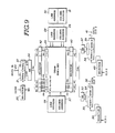
- Figure 9 shows another embodiment of semiconductor memory according to the present invention.
- a selector 42 is provided between the switch circuit 24 and the DRAM 25.
- the selector 42 is divided into 16 blocks corresponding to the blocks 0 to 15 of the DRAM 25.
- the 256-bit data lines are divided by means of the switch circuit 24 into sixteen 16-bit data lines and introducing into each block of the selector 42 corresponding to the block 0 to 15 of the DRAM 25.
- a selector 43 is also provided between the DRAM 25 and the switch circuit 32 and 37.
- the selector 43 is also divided into 16 blocks corresponding to the blocks 0 to 15 of the DRAM 25.
- Each 16-bit data line is introduced through the DRAM 25 into each block of the selector 43 corresponding to the block 0 to 15 of the DRAM 25.
- All 16-bit data lines from the selector 43 are gathered together to make 256-bit data lines which are introduced into the switch circuits 32 and 37.
- the selector 42 is controlled by means of address signals produced by the column-address circuit 27.
- the selector 43 is controlled by means of address signals produced by the column-address circuits 29 and 31.
- the 256-bit data lines are divided by means of the switch circuits 24, 32 or 37 into, for example, two 128-bit data lines horizontally extending from near the centre of the switch circuit 24, 32 or 37 towards the left and right sides, respectively.
- the left-hand 128-bit data lines are introduced into the blocks of the selector 42 or 43 corresponding to the blocks 0 to 7 of the DRAM 25.
- the right-hand 128-bit data lines are introduced into the blocks of the selector 42 or 43 corresponding to the blocks 8 to 15 of the DRAM 25.
- each 16-bit data line selected from the 128-bit data lines extends vertically to be introduced into each block of the selector 42 or 43.
- each of the 16 blocks numbered 0 to 15 of the DRAM 25 is divided into 16 sub-blocks numbered 0 ⁇ to 15 ⁇ as shown in Figure 12.
- the 16 bits of data are written in each of the sub-blocks by means of a block of the selector 42.
- each 16 bits of data written in each of the sub-blocks are read out by means of a block of the selector 43.
- the 256 bits of data obtained at the output terminal of the switch circuit 24 are divided into 16-bit units and each of these 16-bit data units are, in turn, transferred to one of the even sub-blocks, that is, the sub-blocks 0 ⁇ , 2 ⁇ , 4 ⁇ , 6 ⁇ , 8 ⁇ , 10 ⁇ , 12 ⁇ and 14 ⁇ disposed in one of the blocks 0 to 15 of the DRAM 25, by means of each of the blocks of the selector 42.
- the 256 bits of data obtained at the output terminal of the switch circuit 24 are divided into sixteen 16-bit data units and each of these 16-bit data units are, in turn, transferred to one of the odd sub-blocks, that is, the sub-blocks, 1 ⁇ , 3 ⁇ , 5 ⁇ , 7 ⁇ , 9 ⁇ , 11 ⁇ , 13 ⁇ and 15 ⁇ disposed in one of the blocks 0 to 15 of the DRAM 25 by means of each of the blocks of the selector 42.
- the 256 bits of data which are alternately transferred from the SAMs 21 and 22 to the output terminal of the switch circuit 24, are divided into sixteen 16-bit data units and all of the 16-bit data units are simultaneously transferred to the like numbered sub-blocks of the blocks 0 to 15 of the DRAM 25. All of the 16-bits data units written in the like numbered sub-blocks of the blocks 0 to 15 of the DRAM 25 are simultaneously read out to make up 256 bits of data to be transferred to the SAMs 33 and 34 or the SAMs 38 and 39. Therefore, the wiring area between the switch circuit 24 and the selector 42 and between the selector 43 and the switch circuits 32 and 37 can be small.
- SAMs having 256 bits of memory capacity, and a DRAM having 16 horizontal blocks, but other types of SAM and DRAM can be used.
Abstract
Description
- This invention relates to semiconductor memories. More particularly, but not exclusively, the invention relates to semiconductor asynchronous 3-port first-in-first-out (FIFO) memories. Such memories can be used, for example, in image processing in a video tape recorder or television receiver.
- Asynchronous 3-port FIFO memories, which have serial-access memories (SAM) writing and reading out data, line by line, have been previously proposed. Such memories include first, second and third SAMs. The first SAM comprises a selector, a register, which may have, for example, a capacity of 1024 bits, and a first latch circuit. The second SAM comprises a second latch circuit and a first shift register. The third SAM comprises a third latch circuit and a second shift register.
- Writing clock signals CKW are supplied for the selector, the register and the first latch circuit. Several data are supplied to the register by way of an input terminal. When
clear signals CLR 0 are supplied for the selector, the data are cleared to be set to 0. The selector is actuated by means of write enable signals WE. Address signals are formed when clock signals CKW are supplied for the selector. The address signals are supplied to the register by the selector. Serial data from the input terminal are stored in the register at predetermined locations designated by the address signals, and the data stored in the register are temporarily latched in the first latch circuit. - The data latched by the first latch circuit is written, line by line, in a dynamic random-access memory (DRAM) at a predetermined location assigned by address signals produced from a writing address circuit.
- The data written in the DRAM at a predetermined location assigned by address signals produced by a first read-out address circuit are read out, line by line, to be transferred to the second latch circuit to be further transferred to the first shift register. Read-out
clock signals CKR 1 are supplied for the first read-out address circuit, the second latch circuit and the first shift register.Clear signals CLR 1 are also supplied for the first shift register. - The data transferred to the first shift register are shifted by 1 bit whenever the
clock signals CKL 1 are supplied to a first output terminal, to serve as first data. - On the other hand, the data written in the DRAM at a predetermined location assigned by address signals which are produced by a second read-out address circuit, are read out, line by line, to be transferred to the third latch circuit to be further transferred to the second shift register. Read-out
clock signals CKL 2 are supplied for the second address circuit, the third latch circuit and the second shift register.Clear signals CLR 2 are also supplied for the second shift register. - The data transferred to the second shift register are shifted by 1 bit whenever the
clock signals CKL 2 are supplied to a second output terminal to serve as second data. - A first port comprises the selector, the register and the first latch circuit. A second port comprises the second latch circuit and the first shift register. A third port comprises the third latch circuit and the second shift register. As mentioned above, the first, second and third ports can actuate asynchronously of each other.
- However, with the above-mentioned device, there is the disadvantage that the chips forming the SAMs are of relatively large area, so the cost is high. In addition, the device does not have good operating efficiency.
- According to the present invention there is provided a semiconductor memory comprising:
a storage means for storing data;
characterized by:
an input buffer means, which includes a plurality of first memories having equal memory capacity to each other, for supplying data and for transferring said data to said storage means, said first memories each having a memory capacity equal to a fraction of the memory capacity per line of said storage means; and
an output buffer means, which includes a plurality of second memories having equal memory capacity to each other, for storing data which is supplied from said storage means, and for supplying said data, said second memories each having a memory capacity equal to a fraction of the memory capacity per line of said storage means. - According to the present invention there is also provided a semiconductor memory comprising:
an input buffer means for storing input data;
a storage means for storing said data supplied from said input buffer means; and
an output buffer means for storing said data supplied from said storage means and for reading out said data;
characterized by:
a dividing means for dividing data supplied from said input buffer means into smaller data units to be written in said storage means; and a recombining means for recombining said smaller data units supplied from said storage means to be supplied to said output buffer means. - According to the present invention there is also provided a semiconductor memory characterized by:
a storage means, formed with a plurality of blocks per line, for storing data, each of said blocks being formed with a plurality of sub-blocks;
a dividing means for dividing data into smaller units and for simultaneously writing them in sub-blocks numbered by the same numeral as said blocks; and
a recombining means for recombining said smaller data units stored in said storage means at the sub-blocks numbered by the same numeral as said blocks and for reading out the recombined data. - Thus, a preferred embodiment of semiconductor memory according to the present invention includes an input buffer means for storing input data, an output buffer means for storing the data and for supplying the data, and a storage means for storing the data supplied from the input buffer means and for transferring the data to the output buffer means. The input buffer means includes a plurality of memory means having equal memory capacity. The memory means have memory capacity equal to a fraction of the memory capacity per line of the storage means.
- In addition, the semiconductor memory can be connected to first and second address designating means for producing address signals and for designating the location to and from which the data are transferred, respectively.
- The input buffer means can include first and second memory means. In this case, the semiconductor memory can include a first switching means for transferring data stored in the first memory means to the storage means when data are written in the second memory means and for transferring data stored in the second memory means to the storage means when data are written in the first memory means. The output buffer means can include third and fourth memory means. The semiconductor memory can include a second switching means for reading out data written in the third memory means when data supplied from the storage means are transferred to the fourth memory means and for reading out data written in the fourth memory means when data supplied from the storage means are transferred to the third memory means.
- The input and output buffer means preferably comprises a plurality of serial-access memories and the storage means preferably comprises a dynamic random-access memory. In a preferred construction, the semiconductor memory is provided with a toggle means for delaying one of the data transfers in relation to the other, so that the data transfer from the input buffer means to the storage means does not conflict with the data transfer from the storage means to the output buffer means.
- The invention will now be described by way of example with reference to the accompanying drawings, throughout which like parts are referred to by like references, and in which:
- Figure 1 is a block diagram of an embodiment of semiconductor memory according to the present invention;
- Figure 2 is a diagram of a serial-access memory formed by an input buffer means in the memory of Figure 1;
- Figure 3 is a diagram of a serial-access memory formed by an output buffer means in the memory of Figure 1;
- Figure 4 is a block schematic diagram of input buffer means;
- Figure 5 is a schematic diagram of the output buffer;
- Figure 6 is a block diagram of a dynamic random-access memory used in the memory of Figure 1;
- Figure 7 is a diagram showing the timing relationship between the dynamic random-access memory and the serial-access memory of the input buffer means;
- Figure 8 is a diagram showing the timing relationship between the dynamic random-access memory and the serial-access memory of the output buffer means;
- Figure 9 is a block diagram of another embodiment of semiconductor memory according to the present invention;
- Figure 10 is a schematic wiring diagram of a switch and a selector in Figure 9;
- Figure 11 is a detailed writing diagram of Figure 10; and
- Figure 12 is a block diagram of a dynamic random-access memory used in the memory of Figure 9.
- Referring now to the drawings, particularly to Figure 1, the preferred embodiment of semiconductor memory according to the present invention is an asynchronous 3-port FIFO field memory. The semiconductor memory includes a
selector 20. When clear signalsCLR 0 are supplied to theselector 20, the data are set to 0 to be cleared. Theselector 20 is actuated by means of write enable signals WE. When clock signals CKW are supplied to theselector 20, address signals are formed. Theselector 20 is connected to writing serial-access memories (SAMs) 21 and 22 of equal capacity. For example, theSAMs SAMs input terminal 23, the data are written in theSAMs SAMs input terminal 23 are, in turn, written at the addresses designated by the address signals. The data written in theSAMs switch circuit 24 and supplied to a memory means, for example, a dynamic random-access memory (DRAM) 25. The data stored in theSAM 21 is transferred to theDRAM 25 while data is written in theSAM 22 and, conversely, the data stored in theSAM 22 is transferred to theDRAM 25 while data is written in theSAM 21. A first port comprises theselector 20, theSAMs input terminal 23 and theswitch circuit 24. - The
dram 25 may have, for example, 303 lines of capacity in which one line includes 4096 bits (4096 x 303). Each line may, for example, be divided into 16 blocks each having 256 bits. TheDRAM 25 is connected to a writing line-address circuit 26 and a writingcolumn address circuit 27. The line-address circuit 26 produced address signals to designate the line of theDRAM 25 in which the data are to be written. The column-address circuit 27 produces address signals to designate the column of theDRAM 25 in which the data are to be written. As a result, the 256 bits of data from theSAM DRAM 25. - The
DRAM 25 is also connected to a first read-out line-address circuit 28 and a first read-out column-address circuit 29. The line-address circuit 28 produces address signals to designate the line of theDRAM 25 from which the data are to be read out. The column-address circuit 29 produces address signals to designate the column of theDRAM 25 from which the data are to be read out. As a result, the 256 bits of data written in a predetermined block of theDRAM 25 can be read out. - The
dram 25 is further connected to a second read-out line-address circuit 30 and a second read-out column-address circuit 31. The line-address circuit 30 produces address signals to designate the line of theDRAM 25 from which the data are to be read out. The column-address circuit 31 produces address signals to designate the column of theDRAM 25 from which the data are to be read out. As a result, the 256 bits of data written in a predetermined block of theDRAM 25 can be read out. - The output terminal of the
DRAM 25 is connected to aswitch circuit 32. Theswitch circuit 32 is also connected toSAMs SAMs SAMs selector 35, which can operate in a similar manner to theselector 20, and anoutput terminal 36. A first output buffer means, which is a second port, comprises theSAMs selector 35 and theoutput terminal 36. Theaddress circuits DRAM 25 to be read out. The 256 bits of data are selectively picked up by means of theswitch circuit 32 and transferred to theSAM SAM 33 is read out while data supplied from theDRAM 25 is transferred to theSAM 34. Conversely, the data written in theSAM 34 is read out while data supplied from theDRAM 25 are transferred to theSAM 33. Data stored in theSAM selector 35, are supplied to theoutput terminal - The output terminal of the
DRAM 25 is also connected to aswitch circuit 37. Theswitch circuit 37 is also connected toSAMs SAMs SAMs selector 40, which can operate in a similar manner to theselector 20, and anoutput terminal 41. A second output buffer means, which is a third port, comprises theSAMs selector 40 and theoutput terminal 41. Theaddress circuits DRAM 25 to be read out. The 256 bits of data are selectively picked up by theswitch circuit 32 and transferred to theSAM SAM 38 are read out, while data supplied from theDRAM 25 are transferred to theSAM 39. Conversely, the data written in theSAM 39 are read out while data supplied from theDRAM 25 are transferred to theSAM 38. Data stored in theSAM selector 40, are supplied to theoutput terminal - Preferably a toggle means is provided so that the data transfer from the
SAM DRAM 25 does not conflict with the data transfer from theDRAM 25 to theSAM - As shown in Figure 2, the input 4-bit data units can be selected by means of the
selector 20 and written in theSAM - As shown in Figure 3, each 4-bit data unit written in the
SAM selector 35 and supplied. Each 4-bit data unit written in theSAM selector 40 and supplied. - Figure 4 shows the input buffer means for transferring data from the
SAM DRAM 25. In Figure 4, theselector 20 is shown as a single-pole double-throw switch for reasons of convenience. Theselector 20 is associated with theswitch circuit 24. Theswitch circuit 24 engages its contact a when theselector 20 engages its contact a. Conversely, theswitch contact 24 engages its contact b when theselector 20 engages its contact b. Therefore, when both theselector 20 and theswitch circuit 24 engage their contacts a, each of 4-bit data units from theinput terminal 23 are, in turn, written in theSAM 21 and simultaneously the 256-bits data written in theSAM 22 are transferred to theDRAM 25. Conversely, when both theselector 20 and theswitch circuit 24 engage their contacts b, each of 4 bits of data from theinput terminal 23 are, in turn, written in theSAM 22 and simultaneously the 256-bits data written in theSAM 21 are transferred to theDRAM 25. - As shown in Figure 5, the
DRAM 25 may include 303 lines arranged vertically, each of which may be divided into 16 blocks numbered from 0 to 15. One block may have 256 bits of capacity and one line may have 4096 bits (256 x 16) of capacity. Therefore, there is a map comprising 16 columns x 303 lines. - As mentioned above, each of 256-bits data transferred from the
SAMs address circuits - Figure 6 shows the first output buffer means for transferring data from the
DRAM 25 to theSAM selector 35 is shown as a single-pole double-throw switch for reasons of convenience. Theswitch circuit 32 is associated with theselector 35. Theswitch circuit 32 engages its contact a when theselector 35 engages its contact a. Conversely, theswitch circuit 32 engages its contact b when theselector 20 engages its contact b. Therefore, when both theselector 35 and theswitch circuit 32 engage their contact a, the 256 bits of data written in theDRAM 25 at a predetermined block, the line and column of which have been determined by theaddress circuits SAM 33 and simultaneously 256 bits of data written in theSAM 34 are, in turn, supplied 4 bits at a time. On the contrary, when both theselector 35 and theswitch circuit 32 engage their contact b, the 256 bits data written in theDRAM 25 at a predetermined block, the line and column of which have been determined by theaddress circuits SAM 34, and simultaneously the 256 bits of data written in theSAM 33 are, in turn, supplied 4 bits at a time. - Figure 7 shows the timing relationship between the
DRAM 25 and theSAMs CLR 0 are supplied to theselector 20, the 256 bits of data to be written in theDRAM 25 at theblock 0 are written in theSAM 1 serving as a writing SAM, for example, theSAM 21, and simultaneously the 256 bits of data written in theSAM 2 serving as a transferring SAM, for example theSAM 22, are transferred to theblock 15 of theDRAM 25. Secondly, the 256 bits of data to be written in theDRAM 25 at theblock 1 are written in theSAM 2 serving as the writing SAM and simultaneously the 256 bits data written in theSAM 1 serving as the transferring SAM are transferred to theblock 0 of theDRAM 25. Next, the 256 bits of data to be written in theDRAM 25 at theblock 2 are written in theSAM 1 serving as the writing SAM and simultaneously the 256 bits data written in theSAM 2 serving as the transferring SAM are transferred to theblock 1 of theDRAM 25. Data written in one SAM are transferred to theDRAM 25 while data are written in the other SAM. This operation is repeated until the transfer of all of the data has been finished. - Figure 8 shows the timing relationship between the
DRAM 25 and theSAMs CLR selector block 0 of theDRAM 25, which are written in theSAM 1 serving as a read-out SAM, for example theSAM block 1 of theDRAM 25 are transferred to theSAM 2 serving as a transferring SAM, for example, theSAM block 1 of theDRAM 25, which are written in theSAM 2 serving as the read-out SAM, are supplied 4 bits at a time, and simultaneously the 256 bits of data stored in theblock 2 of theDRAM 25 are transferred to theSAM 1 serving as the transferring SAM. Next, the 256 bits of data corresponding to the data stored in theblock 2 of theDRAM 25, which are written in theSAM 1 serving as the read-out SAM, are supplied 4 bits at a time and simultaneously the 256 bits of data stored in theblock 3 of theDRAM 25 are transferred to theSAM 2 serving as the transferring SAM. Data are transferred from theDRAM 25 to one SAM while data written in the other SAM are supplied. This operation is repeated until all of the data have been read out. - With this embodiment, the SAM having 256 bits of capacity, which is a sixteenth part of 4096 bits corresponding to the memory capacity per line, is used, but other types of SAM having a capacity which is a fraction, such as an eighth or fourth part thereof, can also be used.
- Figure 9 shows another embodiment of semiconductor memory according to the present invention. In this embodiment, a
selector 42 is provided between theswitch circuit 24 and theDRAM 25. Theselector 42 is divided into 16 blocks corresponding to theblocks 0 to 15 of theDRAM 25. The 256-bit data lines are divided by means of theswitch circuit 24 into sixteen 16-bit data lines and introducing into each block of theselector 42 corresponding to theblock 0 to 15 of theDRAM 25. Aselector 43 is also provided between theDRAM 25 and theswitch circuit selector 43 is also divided into 16 blocks corresponding to theblocks 0 to 15 of theDRAM 25. Each 16-bit data line is introduced through theDRAM 25 into each block of theselector 43 corresponding to theblock 0 to 15 of theDRAM 25. All 16-bit data lines from theselector 43 are gathered together to make 256-bit data lines which are introduced into theswitch circuits selector 42 is controlled by means of address signals produced by the column-address circuit 27. Theselector 43 is controlled by means of address signals produced by the column-address circuits - As shown in detail in Figure 10, the 256-bit data lines are divided by means of the
switch circuits switch circuit selector blocks 0 to 7 of theDRAM 25. The right-hand 128-bit data lines are introduced into the blocks of theselector blocks 8 to 15 of theDRAM 25. As shown in detail in Figure 11, each 16-bit data line selected from the 128-bit data lines extends vertically to be introduced into each block of theselector - In this embodiment, each of the 16 blocks numbered 0 to 15 of the
DRAM 25 is divided into 16 sub-blocks numbered 0ʹ to 15ʹ as shown in Figure 12. The 16 bits of data are written in each of the sub-blocks by means of a block of theselector 42. On the other hand, each 16 bits of data written in each of the sub-blocks are read out by means of a block of theselector 43. - For example, in order to transfer the 256 bits of data stored in the
SAM 21 to theDRAM 25, the 256 bits of data obtained at the output terminal of theswitch circuit 24 are divided into 16-bit units and each of these 16-bit data units are, in turn, transferred to one of the even sub-blocks, that is, the sub-blocks 0ʹ, 2ʹ, 4ʹ, 6ʹ, 8ʹ, 10ʹ, 12ʹ and 14ʹ disposed in one of theblocks 0 to 15 of theDRAM 25, by means of each of the blocks of theselector 42. On the other hand, in order to transfer the 256 bits of data stored in theSAM 22 to theDRAM 25, the 256 bits of data obtained at the output terminal of theswitch circuit 24 are divided into sixteen 16-bit data units and each of these 16-bit data units are, in turn, transferred to one of the odd sub-blocks, that is, the sub-blocks, 1ʹ, 3ʹ, 5ʹ, 7ʹ, 9ʹ, 11ʹ, 13ʹ and 15ʹ disposed in one of theblocks 0 to 15 of theDRAM 25 by means of each of the blocks of theselector 42. - That is, all the 256 bits of data stored in the
SAM blocks 0 to 15 of theDRAM 25 by means of the blocks of theselector 42. Secondly, all 256 bits of data stored in theSAM blocks 0 to 15 of theDRAM 25 by means of the blocks of theselector 42. This operation is repeated. - Conversely, in order to transfer the data written in the
DRAM 25 to theSAMs blocks 0 to 15 of theDRAM 25 are simultaneously read out by means of the blocks of theselector 43 to be 256 bits (16 x 16) of data to be transferred to theSAM 33 through theswitch circuit 32. - That is, all of the 16-bit data units written in the sub-blocks 0ʹ of the
blocks 0 to 15 of theDRAM 25 are simultaneously read out by means of the blocks of theselector 43 to make up 256 bits of data to be transferred to theSAM 33 through theswitch 32. Secondly, all of the 16-bit data units written in the sub-blocks 1ʹ of theblocks 0 to 15 of theDRAM 25 are simultaneously read out by means of the blocks of theselector 43 to be 256 bits of data so as to be transferred to theSAM 34. This operation is repeated. - When the data written in the
DRAM 25 are transferred to theSAMs - As described above, the 256 bits of data, which are alternately transferred from the
SAMs switch circuit 24, are divided into sixteen 16-bit data units and all of the 16-bit data units are simultaneously transferred to the like numbered sub-blocks of theblocks 0 to 15 of theDRAM 25. All of the 16-bits data units written in the like numbered sub-blocks of theblocks 0 to 15 of theDRAM 25 are simultaneously read out to make up 256 bits of data to be transferred to theSAMs SAMs switch circuit 24 and theselector 42 and between theselector 43 and theswitch circuits - The above description refers to SAMs having 256 bits of memory capacity, and a DRAM having 16 horizontal blocks, but other types of SAM and DRAM can be used.
Claims (18)
a storage means (25) for storing data;
characterized by:
an input buffer means (20 to 22), which includes a plurality of first memories (21, 22) having equal memory capacity to each other, for supplying data and for transferring said data to said storage means (25), said first memories (21, 22) each having a memory capacity equal to a fraction of the memory capacity per line of said storage means (25); and
an output buffer means (33 to 35, 38 to 40), which includes a plurality of second memories (33, 34, 38, 39) having equal memory capacity to each other, for storing data which is supplied from said storage means (25), and for supplying said data, said second memories (33, 34, 38, 39) each having a memory capacity equal to a fraction of the memory capacity per line of said storage means (25).
an input buffer means (20 to 22) for storing input data;
a storage means (25) for storing said data supplied from said input buffer means (20 to 22); and
an output buffer means (33 to 35, 38 to 40) for storing said data supplied from said storage means (25) and for reading out said data;
characterized by:
a dividing means (20) for dividing data supplied from said input buffer means (20 to 22) into smaller data units to be written in said storage means (25); and
a recombining means (35, 40) for recombining said smaller data units supplied from said storage means (25) to be supplied to said output buffer means (33 to 35, 38 to 40).
a storage means (25), formed with a plurality of blocks per line, for storing data, each of said blocks being formed with a plurality of sub-blocks;
a dividing means (20) for dividing data into smaller data units and for simultaneously writing them in sub-blocks numbered by the same numerals as said blocks; and
a recombining means (35, 40) for recombining said smaller data units stored in said storage means (25) at the sub-blocks numbered by the same numeral as said blocks and for reading out the recombined data.
Priority Applications (1)
| Application Number | Priority Date | Filing Date | Title |
|---|---|---|---|
| AT87303753T ATE100223T1 (en) | 1986-04-28 | 1987-04-28 | SEMICONDUCTOR MEMORY. |
Applications Claiming Priority (4)
| Application Number | Priority Date | Filing Date | Title |
|---|---|---|---|
| JP61098847A JPS62256300A (en) | 1986-04-28 | 1986-04-28 | Video storage device |
| JP98847/86 | 1986-04-28 | ||
| JP100044/86 | 1986-04-30 | ||
| JP61100044A JPH0715790B2 (en) | 1986-04-30 | 1986-04-30 | Video storage |
Publications (3)
| Publication Number | Publication Date |
|---|---|
| EP0246767A2 true EP0246767A2 (en) | 1987-11-25 |
| EP0246767A3 EP0246767A3 (en) | 1990-07-18 |
| EP0246767B1 EP0246767B1 (en) | 1994-01-12 |
Family
ID=26439955
Family Applications (1)
| Application Number | Title | Priority Date | Filing Date |
|---|---|---|---|
| EP87303753A Expired - Lifetime EP0246767B1 (en) | 1986-04-28 | 1987-04-28 | Semiconductor memories |
Country Status (5)
| Country | Link |
|---|---|
| US (1) | US5040149A (en) |
| EP (1) | EP0246767B1 (en) |
| CN (1) | CN1009682B (en) |
| CA (1) | CA1293565C (en) |
| DE (1) | DE3788747T2 (en) |
Cited By (9)
| Publication number | Priority date | Publication date | Assignee | Title |
|---|---|---|---|---|
| EP0317963A2 (en) * | 1987-11-25 | 1989-05-31 | Kabushiki Kaisha Toshiba | Semiconductor memory device having dRAM cells |
| EP0319432A2 (en) * | 1987-12-04 | 1989-06-07 | Fujitsu Limited | Semiconductor memory device with serial access memory |
| EP0360243A2 (en) * | 1988-09-21 | 1990-03-28 | Kabushiki Kaisha Toshiba | Video memory device |
| EP0418910A2 (en) * | 1989-09-22 | 1991-03-27 | Kabushiki Kaisha Toshiba | Image memory |
| EP0467004A1 (en) * | 1990-07-17 | 1992-01-22 | STMicroelectronics S.r.l. | A programmable device for storing digital video lines |
| EP0552979A2 (en) * | 1992-01-23 | 1993-07-28 | Samsung Electronics Co., Ltd. | Apparatus and method for de-interleaving data |
| EP0573685A1 (en) * | 1992-06-09 | 1993-12-15 | Siemens Aktiengesellschaft | Integrated semiconductor memory device |
| EP1004956A2 (en) * | 1990-04-18 | 2000-05-31 | Rambus Inc. | Integrated I/O circuit using a high performance bus interface |
| US6182184B1 (en) | 1990-04-18 | 2001-01-30 | Rambus Inc. | Method of operating a memory device having a variable data input length |
Families Citing this family (20)
| Publication number | Priority date | Publication date | Assignee | Title |
|---|---|---|---|---|
| US5408673A (en) * | 1989-10-13 | 1995-04-18 | Texas Instruments Incorporated | Circuit for continuous processing of video signals in a synchronous vector processor and method of operating same |
| JP2880547B2 (en) * | 1990-01-19 | 1999-04-12 | 三菱電機株式会社 | Semiconductor storage device |
| US6324120B2 (en) | 1990-04-18 | 2001-11-27 | Rambus Inc. | Memory device having a variable data output length |
| US6751696B2 (en) | 1990-04-18 | 2004-06-15 | Rambus Inc. | Memory device having a programmable register |
| JP2900523B2 (en) * | 1990-05-31 | 1999-06-02 | 日本電気株式会社 | Write circuit for nonvolatile semiconductor memory device |
| JPH04188243A (en) * | 1990-11-21 | 1992-07-06 | Nippon Steel Corp | Storage device |
| DE69126962D1 (en) * | 1991-05-16 | 1997-09-04 | Ibm | Storage arrangement |
| US5315388A (en) * | 1991-11-19 | 1994-05-24 | General Instrument Corporation | Multiple serial access memory for use in feedback systems such as motion compensated television |
| JPH05274862A (en) * | 1992-03-24 | 1993-10-22 | Mitsubishi Electric Corp | Semiconductor memory device |
| US5745791A (en) * | 1992-09-16 | 1998-04-28 | Intel Corporation | System for interfacing first and second components having different data path width by generating first and second component address to read data into buffer |
| US5544338A (en) * | 1992-12-31 | 1996-08-06 | International Business Machines Corporation | Apparatus and method for raster generation from sparse area array output |
| JP3319637B2 (en) * | 1993-11-10 | 2002-09-03 | 松下電器産業株式会社 | Semiconductor memory device and control method thereof |
| JPH08212132A (en) * | 1995-02-07 | 1996-08-20 | Mitsubishi Electric Corp | Storage device |
| US6378060B1 (en) * | 1998-08-24 | 2002-04-23 | Microunity Systems Engineering, Inc. | System to implement a cross-bar switch of a broadband processor |
| US6532185B2 (en) * | 2001-02-23 | 2003-03-11 | International Business Machines Corporation | Distribution of bank accesses in a multiple bank DRAM used as a data buffer |
| US20060041798A1 (en) * | 2004-08-23 | 2006-02-23 | On-Chip Technologies, Inc. | Design techniques to increase testing efficiency |
| EP3268965A4 (en) | 2015-03-12 | 2018-10-03 | Micron Technology, INC. | Apparatuses and methods for data movement |
| US10048888B2 (en) | 2016-02-10 | 2018-08-14 | Micron Technology, Inc. | Apparatuses and methods for partitioned parallel data movement |
| US10074416B2 (en) | 2016-03-28 | 2018-09-11 | Micron Technology, Inc. | Apparatuses and methods for data movement |
| CN113252217B (en) * | 2021-07-15 | 2021-09-24 | 南京东大智能化系统有限公司 | Stress change monitoring method based on fiber bragg grating |
Citations (1)
| Publication number | Priority date | Publication date | Assignee | Title |
|---|---|---|---|---|
| JPS58133698A (en) * | 1982-02-02 | 1983-08-09 | Nec Corp | Semiconductor memory device |
Family Cites Families (12)
| Publication number | Priority date | Publication date | Assignee | Title |
|---|---|---|---|---|
| JPS58189890A (en) * | 1982-04-30 | 1983-11-05 | Hitachi Ltd | Hierarchical storage device |
| US4541076A (en) * | 1982-05-13 | 1985-09-10 | Storage Technology Corporation | Dual port CMOS random access memory |
| US4541075A (en) * | 1982-06-30 | 1985-09-10 | International Business Machines Corporation | Random access memory having a second input/output port |
| US4630230A (en) * | 1983-04-25 | 1986-12-16 | Cray Research, Inc. | Solid state storage device |
| US4567579A (en) * | 1983-07-08 | 1986-01-28 | Texas Instruments Incorporated | Dynamic memory with high speed nibble mode |
| US4688197A (en) * | 1983-12-30 | 1987-08-18 | Texas Instruments Incorporated | Control of data access to memory for improved video system |
| US4747081A (en) * | 1983-12-30 | 1988-05-24 | Texas Instruments Incorporated | Video display system using memory with parallel and serial access employing serial shift registers selected by column address |
| US4648077A (en) * | 1985-01-22 | 1987-03-03 | Texas Instruments Incorporated | Video serial accessed memory with midline load |
| JPS6216294A (en) * | 1985-07-16 | 1987-01-24 | Fuji Xerox Co Ltd | Memory device |
| KR900002664B1 (en) * | 1985-08-16 | 1990-04-21 | 가부시끼가이샤 히다찌세이사꾸쇼 | The semiconductor memory having serial data |
| US4725987A (en) * | 1985-10-23 | 1988-02-16 | Eastman Kodak Company | Architecture for a fast frame store using dynamic RAMS |
| US4789960A (en) * | 1987-01-30 | 1988-12-06 | Rca Licensing Corporation | Dual port video memory system having semi-synchronous data input and data output |
-
1987
- 1987-04-24 CA CA000535478A patent/CA1293565C/en not_active Expired - Lifetime
- 1987-04-28 EP EP87303753A patent/EP0246767B1/en not_active Expired - Lifetime
- 1987-04-28 DE DE87303753T patent/DE3788747T2/en not_active Expired - Lifetime
- 1987-04-28 CN CN87103783.1A patent/CN1009682B/en not_active Expired
-
1990
- 1990-03-15 US US07/496,076 patent/US5040149A/en not_active Expired - Lifetime
Patent Citations (1)
| Publication number | Priority date | Publication date | Assignee | Title |
|---|---|---|---|---|
| JPS58133698A (en) * | 1982-02-02 | 1983-08-09 | Nec Corp | Semiconductor memory device |
Non-Patent Citations (4)
| Title |
|---|
| IEEE JOURNAL OF SOLID-STATE CIRCUITS, vol. SC-19, no. 6, December 1984, pages 999-1007, IEEE, New York, US; R. PINKHAM et al.: "A high speed dual port memory with simultaneous serial and random mode access for video applications" * |
| PATENT ABSTRACTS OF JAPAN, vol. 7, no. 249 (P-234)[1394], 5th November 1983; & JP 58133698 A (NIPPON DENKI K.K.) 09-08-1983 * |
| SMPTE JOURNAL, vol. 89, no. 4, April 1980, pages 257-262, Scarsdale, US; T. YOSHINO et al.: "Digital frame memory for still picture television receivers PASS encoding system and application" * |
| WESCON TECHNICAL PAPERS, vol. 16, 19th-22nd September 1972, pages 413.1 - 413.5, Western Electronic Show and Convention, Los Angeles, US; Y. HSIA: "Memory applications of the MNOS" * |
Cited By (23)
| Publication number | Priority date | Publication date | Assignee | Title |
|---|---|---|---|---|
| EP0317963A3 (en) * | 1987-11-25 | 1990-09-05 | Kabushiki Kaisha Toshiba | Semiconductor memory device having dram cells |
| EP0317963A2 (en) * | 1987-11-25 | 1989-05-31 | Kabushiki Kaisha Toshiba | Semiconductor memory device having dRAM cells |
| EP0319432A2 (en) * | 1987-12-04 | 1989-06-07 | Fujitsu Limited | Semiconductor memory device with serial access memory |
| EP0319432A3 (en) * | 1987-12-04 | 1990-11-28 | Fujitsu Limited | Semiconductor memory device with serial access memory |
| EP0360243A2 (en) * | 1988-09-21 | 1990-03-28 | Kabushiki Kaisha Toshiba | Video memory device |
| EP0360243A3 (en) * | 1988-09-21 | 1992-04-08 | Kabushiki Kaisha Toshiba | Video memory device |
| US5185724A (en) * | 1989-09-22 | 1993-02-09 | Kabushiki Kaisha Toshiba | Image memory |
| EP0418910A2 (en) * | 1989-09-22 | 1991-03-27 | Kabushiki Kaisha Toshiba | Image memory |
| EP0418910A3 (en) * | 1989-09-22 | 1992-09-16 | Kabushiki Kaisha Toshiba | Image memory |
| US6260097B1 (en) | 1990-04-18 | 2001-07-10 | Rambus | Method and apparatus for controlling a synchronous memory device |
| US6266285B1 (en) | 1990-04-18 | 2001-07-24 | Rambus Inc. | Method of operating a memory device having write latency |
| US6584037B2 (en) | 1990-04-18 | 2003-06-24 | Rambus Inc | Memory device which samples data after an amount of time transpires |
| EP1004956A2 (en) * | 1990-04-18 | 2000-05-31 | Rambus Inc. | Integrated I/O circuit using a high performance bus interface |
| EP1004956A3 (en) * | 1990-04-18 | 2000-06-21 | Rambus Inc. | Integrated I/O circuit using a high performance bus interface |
| US6182184B1 (en) | 1990-04-18 | 2001-01-30 | Rambus Inc. | Method of operating a memory device having a variable data input length |
| US6570814B2 (en) | 1990-04-18 | 2003-05-27 | Rambus Inc. | Integrated circuit device which outputs data after a latency period transpires |
| US6378020B2 (en) | 1990-04-18 | 2002-04-23 | Rambus Inc. | System having double data transfer rate and intergrated circuit therefor |
| US6314051B1 (en) | 1990-04-18 | 2001-11-06 | Rambus Inc. | Memory device having write latency |
| US6304937B1 (en) | 1990-04-18 | 2001-10-16 | Rambus Inc. | Method of operation of a memory controller |
| EP0467004A1 (en) * | 1990-07-17 | 1992-01-22 | STMicroelectronics S.r.l. | A programmable device for storing digital video lines |
| EP0552979B1 (en) * | 1992-01-23 | 2001-07-25 | Samsung Electronics Co., Ltd. | Apparatus and method for de-interleaving data |
| EP0552979A2 (en) * | 1992-01-23 | 1993-07-28 | Samsung Electronics Co., Ltd. | Apparatus and method for de-interleaving data |
| EP0573685A1 (en) * | 1992-06-09 | 1993-12-15 | Siemens Aktiengesellschaft | Integrated semiconductor memory device |
Also Published As
| Publication number | Publication date |
|---|---|
| DE3788747T2 (en) | 1994-05-05 |
| EP0246767A3 (en) | 1990-07-18 |
| US5040149A (en) | 1991-08-13 |
| EP0246767B1 (en) | 1994-01-12 |
| CN1009682B (en) | 1990-09-19 |
| CN87103783A (en) | 1987-11-04 |
| DE3788747D1 (en) | 1994-02-24 |
| CA1293565C (en) | 1991-12-24 |
Similar Documents
| Publication | Publication Date | Title |
|---|---|---|
| EP0246767A2 (en) | Semiconductor memories | |
| US4891794A (en) | Three port random access memory | |
| US5956284A (en) | Method and apparatus for writing to memory components | |
| JPH035991A (en) | Double port-memory | |
| US4845640A (en) | High-speed dual mode graphics memory | |
| US4271483A (en) | Delay circuits | |
| EP0272980A2 (en) | Boundary-free semiconductor memory device | |
| US5117395A (en) | Expansible FIFO memory for accommodating added memory stages in a multistage memory with common control signals | |
| US5349561A (en) | Multiport memory and method of operation thereof | |
| US5325332A (en) | Dual port semiconductor memory device | |
| KR0136747B1 (en) | Semiconductor memory device | |
| US4152781A (en) | Multiplexed and interlaced charge-coupled serial-parallel-serial memory device | |
| KR960000274B1 (en) | Video memory apparatus | |
| EP0617530B1 (en) | Interconnection memory comprising an array of dual-port FIFO memories | |
| US5625594A (en) | Digital video memory | |
| JPS62256300A (en) | Video storage device | |
| US6717624B1 (en) | Line memory in which reading of a preceding line from a first memory and writing of a current line to a second memory are performed in the same time period | |
| US5701271A (en) | Integrated circuit memory devices including banks of memory blocks | |
| US7729198B2 (en) | Synchronous memory circuit | |
| JPH0255877B2 (en) | ||
| JP2961733B2 (en) | Image memory device | |
| JP3154506B2 (en) | Semiconductor device | |
| JP3185278B2 (en) | Orthogonal memory | |
| JPS6299973A (en) | Semiconductor memory device | |
| CN115116512A (en) | Data processing circuit and device |
Legal Events
| Date | Code | Title | Description |
|---|---|---|---|
| PUAI | Public reference made under article 153(3) epc to a published international application that has entered the european phase |
Free format text: ORIGINAL CODE: 0009012 |
|
| AK | Designated contracting states |
Kind code of ref document: A2 Designated state(s): AT DE FR GB IT NL |
|
| PUAL | Search report despatched |
Free format text: ORIGINAL CODE: 0009013 |
|
| AK | Designated contracting states |
Kind code of ref document: A3 Designated state(s): AT DE FR GB IT NL |
|
| 17P | Request for examination filed |
Effective date: 19901128 |
|
| 17Q | First examination report despatched |
Effective date: 19920410 |
|
| GRAA | (expected) grant |
Free format text: ORIGINAL CODE: 0009210 |
|
| AK | Designated contracting states |
Kind code of ref document: B1 Designated state(s): AT DE FR GB IT NL |
|
| REF | Corresponds to: |
Ref document number: 100223 Country of ref document: AT Date of ref document: 19940115 Kind code of ref document: T |
|
| REF | Corresponds to: |
Ref document number: 3788747 Country of ref document: DE Date of ref document: 19940224 |
|
| ITF | It: translation for a ep patent filed |
Owner name: SOCIETA' ITALIANA BREVETTI S.P.A. |
|
| ITTA | It: last paid annual fee | ||
| ET | Fr: translation filed | ||
| PLBE | No opposition filed within time limit |
Free format text: ORIGINAL CODE: 0009261 |
|
| STAA | Information on the status of an ep patent application or granted ep patent |
Free format text: STATUS: NO OPPOSITION FILED WITHIN TIME LIMIT |
|
| 26N | No opposition filed | ||
| REG | Reference to a national code |
Ref country code: GB Ref legal event code: IF02 |
|
| PGFP | Annual fee paid to national office [announced via postgrant information from national office to epo] |
Ref country code: NL Payment date: 20060403 Year of fee payment: 20 |
|
| PGFP | Annual fee paid to national office [announced via postgrant information from national office to epo] |
Ref country code: FR Payment date: 20060410 Year of fee payment: 20 |
|
| PGFP | Annual fee paid to national office [announced via postgrant information from national office to epo] |
Ref country code: AT Payment date: 20060412 Year of fee payment: 20 |
|
| PGFP | Annual fee paid to national office [announced via postgrant information from national office to epo] |
Ref country code: DE Payment date: 20060420 Year of fee payment: 20 |
|
| PGFP | Annual fee paid to national office [announced via postgrant information from national office to epo] |
Ref country code: GB Payment date: 20060426 Year of fee payment: 20 |
|
| PGFP | Annual fee paid to national office [announced via postgrant information from national office to epo] |
Ref country code: IT Payment date: 20060430 Year of fee payment: 20 |
|
| PG25 | Lapsed in a contracting state [announced via postgrant information from national office to epo] |
Ref country code: NL Free format text: LAPSE BECAUSE OF EXPIRATION OF PROTECTION Effective date: 20070428 |
|
| REG | Reference to a national code |
Ref country code: GB Ref legal event code: PE20 |
|
| NLV7 | Nl: ceased due to reaching the maximum lifetime of a patent |
Effective date: 20070428 |
|
| PG25 | Lapsed in a contracting state [announced via postgrant information from national office to epo] |
Ref country code: GB Free format text: LAPSE BECAUSE OF EXPIRATION OF PROTECTION Effective date: 20070427 |