EP0258056A2 - Integrated circuit package having coaxial pins - Google Patents
Integrated circuit package having coaxial pins Download PDFInfo
- Publication number
- EP0258056A2 EP0258056A2 EP87307594A EP87307594A EP0258056A2 EP 0258056 A2 EP0258056 A2 EP 0258056A2 EP 87307594 A EP87307594 A EP 87307594A EP 87307594 A EP87307594 A EP 87307594A EP 0258056 A2 EP0258056 A2 EP 0258056A2
- Authority
- EP
- European Patent Office
- Prior art keywords
- pins
- coaxial pins
- coaxial
- integrated circuit
- circuit package
- Prior art date
- Legal status (The legal status is an assumption and is not a legal conclusion. Google has not performed a legal analysis and makes no representation as to the accuracy of the status listed.)
- Granted
Links
Images


Classifications
-
- H—ELECTRICITY
- H01—ELECTRIC ELEMENTS
- H01L—SEMICONDUCTOR DEVICES NOT COVERED BY CLASS H10
- H01L21/00—Processes or apparatus adapted for the manufacture or treatment of semiconductor or solid state devices or of parts thereof
- H01L21/02—Manufacture or treatment of semiconductor devices or of parts thereof
- H01L21/04—Manufacture or treatment of semiconductor devices or of parts thereof the devices having at least one potential-jump barrier or surface barrier, e.g. PN junction, depletion layer or carrier concentration layer
- H01L21/48—Manufacture or treatment of parts, e.g. containers, prior to assembly of the devices, using processes not provided for in a single one of the subgroups H01L21/06 - H01L21/326
- H01L21/4814—Conductive parts
- H01L21/4885—Wire-like parts or pins
-
- H—ELECTRICITY
- H01—ELECTRIC ELEMENTS
- H01L—SEMICONDUCTOR DEVICES NOT COVERED BY CLASS H10
- H01L23/00—Details of semiconductor or other solid state devices
- H01L23/48—Arrangements for conducting electric current to or from the solid state body in operation, e.g. leads, terminal arrangements ; Selection of materials therefor
- H01L23/50—Arrangements for conducting electric current to or from the solid state body in operation, e.g. leads, terminal arrangements ; Selection of materials therefor for integrated circuit devices, e.g. power bus, number of leads
-
- H—ELECTRICITY
- H01—ELECTRIC ELEMENTS
- H01L—SEMICONDUCTOR DEVICES NOT COVERED BY CLASS H10
- H01L23/00—Details of semiconductor or other solid state devices
- H01L23/52—Arrangements for conducting electric current within the device in operation from one component to another, i.e. interconnections, e.g. wires, lead frames
- H01L23/538—Arrangements for conducting electric current within the device in operation from one component to another, i.e. interconnections, e.g. wires, lead frames the interconnection structure between a plurality of semiconductor chips being formed on, or in, insulating substrates
- H01L23/5384—Conductive vias through the substrate with or without pins, e.g. buried coaxial conductors
-
- H—ELECTRICITY
- H01—ELECTRIC ELEMENTS
- H01L—SEMICONDUCTOR DEVICES NOT COVERED BY CLASS H10
- H01L2224/00—Indexing scheme for arrangements for connecting or disconnecting semiconductor or solid-state bodies and methods related thereto as covered by H01L24/00
- H01L2224/01—Means for bonding being attached to, or being formed on, the surface to be connected, e.g. chip-to-package, die-attach, "first-level" interconnects; Manufacturing methods related thereto
- H01L2224/10—Bump connectors; Manufacturing methods related thereto
- H01L2224/15—Structure, shape, material or disposition of the bump connectors after the connecting process
- H01L2224/16—Structure, shape, material or disposition of the bump connectors after the connecting process of an individual bump connector
- H01L2224/161—Disposition
- H01L2224/16151—Disposition the bump connector connecting between a semiconductor or solid-state body and an item not being a semiconductor or solid-state body, e.g. chip-to-substrate, chip-to-passive
- H01L2224/16221—Disposition the bump connector connecting between a semiconductor or solid-state body and an item not being a semiconductor or solid-state body, e.g. chip-to-substrate, chip-to-passive the body and the item being stacked
- H01L2224/16225—Disposition the bump connector connecting between a semiconductor or solid-state body and an item not being a semiconductor or solid-state body, e.g. chip-to-substrate, chip-to-passive the body and the item being stacked the item being non-metallic, e.g. insulating substrate with or without metallisation
-
- H—ELECTRICITY
- H01—ELECTRIC ELEMENTS
- H01L—SEMICONDUCTOR DEVICES NOT COVERED BY CLASS H10
- H01L2924/00—Indexing scheme for arrangements or methods for connecting or disconnecting semiconductor or solid-state bodies as covered by H01L24/00
- H01L2924/01—Chemical elements
- H01L2924/01019—Potassium [K]
-
- H—ELECTRICITY
- H01—ELECTRIC ELEMENTS
- H01L—SEMICONDUCTOR DEVICES NOT COVERED BY CLASS H10
- H01L2924/00—Indexing scheme for arrangements or methods for connecting or disconnecting semiconductor or solid-state bodies as covered by H01L24/00
- H01L2924/15—Details of package parts other than the semiconductor or other solid state devices to be connected
- H01L2924/151—Die mounting substrate
- H01L2924/153—Connection portion
- H01L2924/1531—Connection portion the connection portion being formed only on the surface of the substrate opposite to the die mounting surface
- H01L2924/15312—Connection portion the connection portion being formed only on the surface of the substrate opposite to the die mounting surface being a pin array, e.g. PGA
-
- H—ELECTRICITY
- H01—ELECTRIC ELEMENTS
- H01L—SEMICONDUCTOR DEVICES NOT COVERED BY CLASS H10
- H01L2924/00—Indexing scheme for arrangements or methods for connecting or disconnecting semiconductor or solid-state bodies as covered by H01L24/00
- H01L2924/30—Technical effects
- H01L2924/301—Electrical effects
- H01L2924/3011—Impedance
-
- H—ELECTRICITY
- H01—ELECTRIC ELEMENTS
- H01L—SEMICONDUCTOR DEVICES NOT COVERED BY CLASS H10
- H01L2924/00—Indexing scheme for arrangements or methods for connecting or disconnecting semiconductor or solid-state bodies as covered by H01L24/00
- H01L2924/30—Technical effects
- H01L2924/301—Electrical effects
- H01L2924/3025—Electromagnetic shielding
Definitions
- the present invention relates to integrated circuit packages, and more specifically to an integrated circuit package suitable for high speed processors.
- Propagation delays caused by interconnecting wires between logic gates are a major contributing factor in the overall speed of integrated circuitry.
- Wire delays on LSI chips become increasingly important as circuit density and speed increase. In high speed processors, the wire delay can account for half the overall delay of the system.
- the integrated circuit package of the present invention comprises a multilayer substrate for mounting a plurality of integrated circuit chips on a first surface thereof, the multilayer substrate having a power supply layer, a ground connection layer and circuit patterns and means for connecting terminals of the chips to the layers.
- An array of coaxial pins is juxtaposed on a second surface of the multilayer substrate opposite to the first surface.
- Each of the coaxial pins comprises an inner conductor and an outer conductor surrounding the inner conductor.
- the inner conductor of one or more of the coaxial pins is connected to the power supply layer and the inner conductors of the remaining coaxial pins are connected to the circuit patterns, the outer conductors of all of the coxial pins being connected to the ground connection layer. Since the inner conductor through which signals are conducted is electrically shielded by the grounded outer conductor, the waveform distortion and crostalk problems can be successfully eliminated. Since the outer conductor is used for ground connection, space saving can be achieved.
- an integrated circuit package comprises a multilayer ceramic substrate 1 and a plurality of integrated circuit chips 2 mounted on the upper surface of the multilayer substrate 1.
- An array of coaxial pins 3 of identical construction are brazed to connecting pads on the lower surface of the substrate 1.
- Multilayer substrate 1 is fabricated by a known multilayer ceramic technology in which a ceramic slurry of a ceramic powder (mixture of alumina and glass) and polymer binder is first prepared, then cast into thin sheets by passing through sheet forming machines. After drying, the sheets are cut to size, via holes are mechanically punched into the sheet, and custom wiring paths are formed by screening a slurry of tungsten or molybdenum onto the surface of the sheet and the via holes are filled with metal.
- Several of these sheets are precisely aligned and press-laminated together and the entire structure is fired at an elevated temperature to form a monolithic sintered body.
- Multilayer substrate 1 comprises one or more power layers 4 and a ground layer 5. Integrated circuit chips 2 are appropriately connected to power layers 4 and ground layer 5 through terminals 6. Printed circuit patterns 7 are formed between such layers to connect chip terminals 6 to pins 3.
- each of the coaxial pins 3 is constructed of an inner conductor 8 and an outer conductor 9 having either a circular or rectangular cross-section.
- Coaxial pins 3 function as input/output pins or power pins.
- the inner conductor 8 of each input/output pin is connected to an appropriate circuit pattern 7 and the inner conductor 8 of each power pin is connected to one of the power layers 4.
- the outer conductors 9 of both input/output pins and power pins are connected to the gound layer 5. Brazing technique is used to accomplish such electrical connections.
- each input/output pin 3 Since the inner conductor 8 of each input/output pin 3 is electrically shielded by the outer conductor 9 which is grounded, the present invention completely eliminates waveform distortion and crosstalk which would otherwise occur as a result of high speed processing of signals.
- a further advantage of this invention is that since ground connection is integrated with either input/output connection and power connection, the coaxial pins 3 can be arranged in a given area with a higher packing density than that achieved with the prior art pin construction.
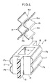
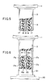
- Figs. 3 to 6 are illustrations of an embodiment which facilitates connection of the coaxial pins 3 to a mother board.
- coaxial pins 3 are arranged in a matrix of rows and columns and each pin is of a rectangular construction and formed with a pair of slits 10 on opposite walls, the slits 10 being aligned with those of adjacent pins 3.
- a pin connector 11 which comprises a series of connector sections 12 which are interconnected by insulative coupling sections or arms 13.
- each connector section 12 is formed of opposed side portions 14 and opposed end portions 15 both of insulative material.
- Inner electrical spring contacts 16 are secured one on each inner wall of side portions 14 and outer electrical spring contacts 17 are secured one on each outer wall of side portions 14.
- Each of the inner contacts 16 has an upper contact portion 16a and a lower contact portion 16b.
- each of the outer contacts 17 has an upper contact portion 17a and a lower contact portion 17b.
- connector sections 12 Prior to connection to a mother board, connector sections 12 are respectively engaged with coaxial pins 3 of each row as shown in Fig. 5, with the coupling sections 13 being slidably fitted into the slits 10 of the corresponding pin 3, and the inner and outer spring contacts 16 and 17 being in pressure contact with the inner and outer conductors 8 and 9 of the corresponding coaxial pin 3, respectively.
- a mother board 20 is provided with an array of coaxial pins 21 identical in construction to the coaxial pins 3 and arranged in positions corresponding to associated coaxial pins 3.
- Each coaxial pin 21 of the mother board has an inner conductor 22 and an outer conductor 23 of the same size as the inner and outer conductors of the corresponding coaxial pin 3.
- the outer conductor 23 of each coaxial pin 21 is formed with slits 24 in positions which aligns with the slits 10 of the corresponding coaxial pin 3.
- the lower contact portions 16b of inner contacts 16 are brought into pressure contact with the inner conductor 22 of coaxial pin 21 with the upper contact portions 16a remaining in pressure contact with the inner conductor 8 of coaxial pin 3, and the lower contact portions 17b of outer contacts 17 are brought into pressure contact with the outer conductor 23 of coaxial pin 21 with the upper contact portions 17a remaining in pressure contact with the outer conductor 9 of coaxial pin 3, whereby electrical connections are established between the inner conductors 8 and 22 and between the outer conductors 9 and 23 of the corresponding pins.
Abstract
Description
- The present invention relates to integrated circuit packages, and more specifically to an integrated circuit package suitable for high speed processors.
- Propagation delays caused by interconnecting wires between logic gates are a major contributing factor in the overall speed of integrated circuitry. Wire delays on LSI chips become increasingly important as circuit density and speed increase. In high speed processors, the wire delay can account for half the overall delay of the system. As circuit density increases there is a corresponding increase in the number of input/output pins according to the known empirical formula P=kGr, where P represents the pin count, G represents the number of gates, and k and r are constants. If it is desired to mount 5000 gates on a single package, for example, more than 2300 input/output pins would be required. Furthermore, for uniform power distribution the same number of power supply pins would be required.
- In a known LSI package as disclosed in U.S. Patent 4,612,601 issued to T. Watari, input/output pins are juxtaposed in alternate relationship with power supply and ground connection pins, requiring a substantial amount of surface area. In addition, for high speed processing, the problems of waveform distortion and crosstalk arise due to mismatched impedances at the input/output pins.
- It is therefore an object of the present invention to provide an integrated circuit package having a high density pin array which is free from waveform distortion and crosstalk.
- Specifically, the integrated circuit package of the present invention comprises a multilayer substrate for mounting a plurality of integrated circuit chips on a first surface thereof, the multilayer substrate having a power supply layer, a ground connection layer and circuit patterns and means for connecting terminals of the chips to the layers. An array of coaxial pins is juxtaposed on a second surface of the multilayer substrate opposite to the first surface. Each of the coaxial pins comprises an inner conductor and an outer conductor surrounding the inner conductor. The inner conductor of one or more of the coaxial pins is connected to the power supply layer and the inner conductors of the remaining coaxial pins are connected to the circuit patterns, the outer conductors of all of the coxial pins being connected to the ground connection layer. Since the inner conductor through which signals are conducted is electrically shielded by the grounded outer conductor, the waveform distortion and crostalk problems can be successfully eliminated. Since the outer conductor is used for ground connection, space saving can be achieved.
- The present invention will be described in further detail with reference to the accompanying drawings, in which:
- Fig. 1 is a side view of an integrated circuit package according to the present invention;
- Fig. 2 is an enlarged view of the pins of Fig. 1;
- Fig. 3 is a perspective view of the integrated circuit package with associated pin connectors and a mother board;
- Fig. 4 is an exploded, perspective view of a section of the pin connectors of Fig. 3;
- Fig. 5 is a cross-sectional view of a pin accommodating a pin connector; and
- Fig. 6 is a cross-sectional view of associated pins on the integrated circuit package and mother board being electrically interconnected by the pin connector.
- Referring to Fig. 1, an integrated circuit package according to the invention comprises a multilayer ceramic substrate 1 and a plurality of
integrated circuit chips 2 mounted on the upper surface of the multilayer substrate 1. An array ofcoaxial pins 3 of identical construction are brazed to connecting pads on the lower surface of the substrate 1. Multilayer substrate 1 is fabricated by a known multilayer ceramic technology in which a ceramic slurry of a ceramic powder (mixture of alumina and glass) and polymer binder is first prepared, then cast into thin sheets by passing through sheet forming machines. After drying, the sheets are cut to size, via holes are mechanically punched into the sheet, and custom wiring paths are formed by screening a slurry of tungsten or molybdenum onto the surface of the sheet and the via holes are filled with metal. Several of these sheets are precisely aligned and press-laminated together and the entire structure is fired at an elevated temperature to form a monolithic sintered body. - Multilayer substrate 1 comprises one or
more power layers 4 and aground layer 5.Integrated circuit chips 2 are appropriately connected topower layers 4 andground layer 5 throughterminals 6. Printedcircuit patterns 7 are formed between such layers to connectchip terminals 6 topins 3. - As shown in Fig. 2, each of the
coaxial pins 3 is constructed of aninner conductor 8 and anouter conductor 9 having either a circular or rectangular cross-section.Coaxial pins 3 function as input/output pins or power pins. Theinner conductor 8 of each input/output pin is connected to anappropriate circuit pattern 7 and theinner conductor 8 of each power pin is connected to one of thepower layers 4. Theouter conductors 9 of both input/output pins and power pins are connected to thegound layer 5. Brazing technique is used to accomplish such electrical connections. - Since the
inner conductor 8 of each input/output pin 3 is electrically shielded by theouter conductor 9 which is grounded, the present invention completely eliminates waveform distortion and crosstalk which would otherwise occur as a result of high speed processing of signals. A further advantage of this invention is that since ground connection is integrated with either input/output connection and power connection, thecoaxial pins 3 can be arranged in a given area with a higher packing density than that achieved with the prior art pin construction. - Figs. 3 to 6 are illustrations of an embodiment which facilitates connection of the
coaxial pins 3 to a mother board. As shown in Fig. 3,coaxial pins 3 are arranged in a matrix of rows and columns and each pin is of a rectangular construction and formed with a pair ofslits 10 on opposite walls, theslits 10 being aligned with those ofadjacent pins 3. For each row of the pin array is provided a pin connector 11 which comprises a series ofconnector sections 12 which are interconnected by insulative coupling sections orarms 13. As illustrated in detail in Fig. 4, eachconnector section 12 is formed ofopposed side portions 14 and opposedend portions 15 both of insulative material. Innerelectrical spring contacts 16 are secured one on each inner wall ofside portions 14 and outerelectrical spring contacts 17 are secured one on each outer wall ofside portions 14. Each of theinner contacts 16 has anupper contact portion 16a and alower contact portion 16b. Likewise, each of theouter contacts 17 has anupper contact portion 17a and alower contact portion 17b. - Prior to connection to a mother board,
connector sections 12 are respectively engaged withcoaxial pins 3 of each row as shown in Fig. 5, with thecoupling sections 13 being slidably fitted into theslits 10 of thecorresponding pin 3, and the inner andouter spring contacts outer conductors coaxial pin 3, respectively. - A
mother board 20 is provided with an array ofcoaxial pins 21 identical in construction to thecoaxial pins 3 and arranged in positions corresponding to associatedcoaxial pins 3. Eachcoaxial pin 21 of the mother board has aninner conductor 22 and anouter conductor 23 of the same size as the inner and outer conductors of the correspondingcoaxial pin 3. Theouter conductor 23 of eachcoaxial pin 21 is formed withslits 24 in positions which aligns with theslits 10 of the correspondingcoaxial pin 3. - When connection is made between the
coaxial pins coupling arms 13 partially slide out of theslits 10 ofupper pins 3 into theslits 24 of thelower pins 21. This slide movement can be made by applying force to thecoupling arms 13. As illustrated in Fig. 6, thelower contact portions 16b ofinner contacts 16 are brought into pressure contact with theinner conductor 22 ofcoaxial pin 21 with theupper contact portions 16a remaining in pressure contact with theinner conductor 8 ofcoaxial pin 3, and thelower contact portions 17b ofouter contacts 17 are brought into pressure contact with theouter conductor 23 ofcoaxial pin 21 with theupper contact portions 17a remaining in pressure contact with theouter conductor 9 ofcoaxial pin 3, whereby electrical connections are established between theinner conductors outer conductors - The foregoing description shows only preferred embodiments of the present invention. Various modifications are apparent to those skilled in the art without departing from the scope of the present invention which is only limited by the appended claims. Therefore, the embodiments shown and described are only illustrative, not restrictive.
Claims (5)
a multilayer substrate for mounting a plurality of integrated circuit chips on a first surface thereof, said multilayer substrate having a power supply layer, a ground connection layer and circuit patterns and means for connecting terminals of said chips to said layers; and
an array of coaxial pins juxtaposed on a second surface of said multilayer substrate opposite to said first surface, each of said coaxial pins comprising an inner conductor and an outer conductor surrounding the inner conductor, the inner conductor of one or more of said coaxial pins being connected to said power supply layer, the inner conductors of the remaining coaxial pins being connected to said circuit patterns, and the outer conductors of all of said coxial pins being connected to said ground connection layer.
Applications Claiming Priority (2)
| Application Number | Priority Date | Filing Date | Title |
|---|---|---|---|
| JP200788/86 | 1986-08-27 | ||
| JP61200788A JPH0734455B2 (en) | 1986-08-27 | 1986-08-27 | Multilayer wiring board |
Publications (3)
| Publication Number | Publication Date |
|---|---|
| EP0258056A2 true EP0258056A2 (en) | 1988-03-02 |
| EP0258056A3 EP0258056A3 (en) | 1988-09-07 |
| EP0258056B1 EP0258056B1 (en) | 1991-11-06 |
Family
ID=16430200
Family Applications (1)
| Application Number | Title | Priority Date | Filing Date |
|---|---|---|---|
| EP87307594A Expired EP0258056B1 (en) | 1986-08-27 | 1987-08-27 | Integrated circuit package having coaxial pins |
Country Status (6)
| Country | Link |
|---|---|
| US (1) | US4819131A (en) |
| EP (1) | EP0258056B1 (en) |
| JP (1) | JPH0734455B2 (en) |
| AU (1) | AU592518B2 (en) |
| CA (1) | CA1269763A (en) |
| DE (1) | DE3774370D1 (en) |
Cited By (2)
| Publication number | Priority date | Publication date | Assignee | Title |
|---|---|---|---|---|
| GB2225670A (en) * | 1988-11-30 | 1990-06-06 | Hitachi Ltd | Carrier substrate for electrical circuit element |
| AT1695U1 (en) * | 1996-07-29 | 1997-09-25 | Mikroelektronik Ges Mit Beschr | SWITCHING ARRANGEMENT |
Families Citing this family (20)
| Publication number | Priority date | Publication date | Assignee | Title |
|---|---|---|---|---|
| JPH0821450B2 (en) * | 1987-10-05 | 1996-03-04 | 日本電気株式会社 | High-speed signal connector |
| JPH0519995Y2 (en) * | 1988-01-05 | 1993-05-25 | ||
| JPH0677469B2 (en) * | 1988-12-28 | 1994-09-28 | 日本電気株式会社 | Multi-contact connector guide structure |
| US4912772A (en) * | 1989-03-06 | 1990-03-27 | International Business Machines Corporation | Connector and circuit package apparatus for pin array circuit module and circuit board |
| JPH0744240B2 (en) * | 1990-11-30 | 1995-05-15 | 工業技術院長 | How to connect the motherboard and chip carrier |
| JPH04351710A (en) * | 1991-05-30 | 1992-12-07 | Sony Corp | Rotary head drum device |
| US5334030A (en) * | 1992-06-01 | 1994-08-02 | National Semiconductor Corporation | PCMCIA bus extender card for PCMCIA system development |
| JPH06314580A (en) * | 1992-08-05 | 1994-11-08 | Amp Japan Ltd | Coaxial connection for two boards connection |
| JPH0828244B2 (en) * | 1993-04-28 | 1996-03-21 | 日本電気株式会社 | Multi-chip package power supply structure |
| US5791911A (en) * | 1996-10-25 | 1998-08-11 | International Business Machines Corporation | Coaxial interconnect devices and methods of making the same |
| US6137693A (en) * | 1998-07-31 | 2000-10-24 | Agilent Technologies Inc. | High-frequency electronic package with arbitrarily-shaped interconnects and integral shielding |
| US20040043644A1 (en) * | 1999-11-02 | 2004-03-04 | Dibene J. Ted | Coaxial and linear power delivery devices |
| US6803650B2 (en) * | 2001-02-23 | 2004-10-12 | Silicon Bandwidth Inc. | Semiconductor die package having mesh power and ground planes |
| DE10164799B4 (en) * | 2001-03-21 | 2006-03-30 | Audioton Kabelwerk Gmbh | Mobile telephone device with multicore electrical connection devices |
| US20040173894A1 (en) * | 2001-09-27 | 2004-09-09 | Amkor Technology, Inc. | Integrated circuit package including interconnection posts for multiple electrical connections |
| US6954984B2 (en) * | 2002-07-25 | 2005-10-18 | International Business Machines Corporation | Land grid array structure |
| JP4771808B2 (en) * | 2003-09-24 | 2011-09-14 | イビデン株式会社 | Semiconductor device |
| US7544070B2 (en) * | 2004-07-02 | 2009-06-09 | Seagate Technology Llc | Electrical connector defining a power plane |
| US8064224B2 (en) * | 2008-03-31 | 2011-11-22 | Intel Corporation | Microelectronic package containing silicon patches for high density interconnects, and method of manufacturing same |
| US8465297B2 (en) | 2010-09-25 | 2013-06-18 | Intel Corporation | Self referencing pin |
Citations (4)
| Publication number | Priority date | Publication date | Assignee | Title |
|---|---|---|---|---|
| US3698082A (en) * | 1966-04-25 | 1972-10-17 | Texas Instruments Inc | Complex circuit array method |
| FR2555812A1 (en) * | 1983-11-30 | 1985-05-31 | Nec Corp | BLOCK OF INTEGRATED CIRCUIT CHIPS |
| JPS61288446A (en) * | 1985-06-17 | 1986-12-18 | Fujitsu Ltd | High-speed ic package structure |
| JPS6242437A (en) * | 1985-08-19 | 1987-02-24 | Fujitsu Ltd | Connection structure for micorwave ic |
Family Cites Families (5)
| Publication number | Priority date | Publication date | Assignee | Title |
|---|---|---|---|---|
| US4231629A (en) * | 1979-01-18 | 1980-11-04 | Telex Computer Products, Inc. | Apparatus for connection of coaxial cables to a printed circuit mother board |
| NL8303268A (en) * | 1983-09-23 | 1985-04-16 | Philips Nv | METHOD FOR MANUFACTURING A SEMICONDUCTOR DEVICE AND SEMICONDUCTOR DEVICE MADE BY THE USE OF SUCH A METHOD |
| US4692839A (en) * | 1985-06-24 | 1987-09-08 | Digital Equipment Corporation | Multiple chip interconnection system and package |
| SE450065B (en) * | 1985-10-03 | 1987-06-01 | Ericsson Telefon Ab L M | COAXIAL CONTACT INTENDED TO BE USED AT A TRANSITION BETWEEN A COAXIAL CONTRACTOR AND A PLAN conductor |
| US4814855A (en) * | 1986-04-29 | 1989-03-21 | International Business Machines Corporation | Balltape structure for tape automated bonding, multilayer packaging, universal chip interconnection and energy beam processes for manufacturing balltape |
-
1986
- 1986-08-27 JP JP61200788A patent/JPH0734455B2/en not_active Expired - Lifetime
-
1987
- 1987-08-26 CA CA000545375A patent/CA1269763A/en not_active Expired - Fee Related
- 1987-08-26 US US07/089,530 patent/US4819131A/en not_active Expired - Fee Related
- 1987-08-27 DE DE8787307594T patent/DE3774370D1/en not_active Expired - Fee Related
- 1987-08-27 AU AU77632/87A patent/AU592518B2/en not_active Ceased
- 1987-08-27 EP EP87307594A patent/EP0258056B1/en not_active Expired
Patent Citations (4)
| Publication number | Priority date | Publication date | Assignee | Title |
|---|---|---|---|---|
| US3698082A (en) * | 1966-04-25 | 1972-10-17 | Texas Instruments Inc | Complex circuit array method |
| FR2555812A1 (en) * | 1983-11-30 | 1985-05-31 | Nec Corp | BLOCK OF INTEGRATED CIRCUIT CHIPS |
| JPS61288446A (en) * | 1985-06-17 | 1986-12-18 | Fujitsu Ltd | High-speed ic package structure |
| JPS6242437A (en) * | 1985-08-19 | 1987-02-24 | Fujitsu Ltd | Connection structure for micorwave ic |
Non-Patent Citations (3)
| Title |
|---|
| ELECTRONICS, vol. 59, no. 4, 27th January 1986, pages 56-57, New York, US; "Embedded coaxial wires speed printed-circuit board" * |
| PATENT ABSTRACTS OF JAPAN, vol. 11, no. 152 (E-507)[2599], 16th May 1987; & JP-A-61 288 446 (FUJITSU LTD.) 18-12-1986 * |
| PATENT ABSTRACTS OF JAPAN, vol. 11, no. 224 (E-525)[2671], 21st July 1987; & JP-A-62 042 437 (FUJITSU LTD.) 24-02-1987 * |
Cited By (3)
| Publication number | Priority date | Publication date | Assignee | Title |
|---|---|---|---|---|
| GB2225670A (en) * | 1988-11-30 | 1990-06-06 | Hitachi Ltd | Carrier substrate for electrical circuit element |
| GB2225670B (en) * | 1988-11-30 | 1992-08-19 | Hitachi Ltd | Carrier substrate and method for preparing the same |
| AT1695U1 (en) * | 1996-07-29 | 1997-09-25 | Mikroelektronik Ges Mit Beschr | SWITCHING ARRANGEMENT |
Also Published As
| Publication number | Publication date |
|---|---|
| JPH0734455B2 (en) | 1995-04-12 |
| DE3774370D1 (en) | 1991-12-12 |
| JPS6356949A (en) | 1988-03-11 |
| AU592518B2 (en) | 1990-01-11 |
| EP0258056A3 (en) | 1988-09-07 |
| AU7763287A (en) | 1988-03-03 |
| EP0258056B1 (en) | 1991-11-06 |
| CA1269763A (en) | 1990-05-29 |
| US4819131A (en) | 1989-04-04 |
Similar Documents
| Publication | Publication Date | Title |
|---|---|---|
| US4819131A (en) | Integrated circuit package having coaxial pins | |
| US5007841A (en) | Integrated-circuit chip interconnection system | |
| CA1143862A (en) | High performance semiconductor package assembly | |
| US5593322A (en) | Leadless high density connector | |
| US5701233A (en) | Stackable modules and multimodular assemblies | |
| US4581679A (en) | Multi-element circuit construction | |
| JP4567038B2 (en) | Circuit board layout of high-speed differential signal edge card connector | |
| US4574331A (en) | Multi-element circuit construction | |
| US5019945A (en) | Backplane interconnection system | |
| US4739125A (en) | Electric component part having lead terminals | |
| EP0309942A2 (en) | Multilayer ceramic package with high frequency connections | |
| EP0357758B1 (en) | Hermetic package for integrated circuit chips | |
| US4772864A (en) | Multilayer circuit prototyping board | |
| US4814857A (en) | Circuit module with separate signal and power connectors | |
| US4695810A (en) | Waffleline-configured microwave transmission link | |
| US6310392B1 (en) | Stacked micro ball grid array packages | |
| US4874086A (en) | Film carrier and a method for manufacturing a semiconductor device utilizing the same | |
| US5861664A (en) | LSI package and manufacturing method thereof | |
| JP3084209B2 (en) | Electronic component and manufacturing method thereof | |
| US4583150A (en) | Printed circuit boards | |
| EP0444820A2 (en) | MMIC package and connection | |
| US4851793A (en) | Waffleline - configured transmission link | |
| EP0569528A4 (en) | Electrical connectors | |
| EP0352805A2 (en) | Distributed constant type delay line device and a manufacturing method thereof | |
| JP2564297B2 (en) | Circuit board |
Legal Events
| Date | Code | Title | Description |
|---|---|---|---|
| PUAI | Public reference made under article 153(3) epc to a published international application that has entered the european phase |
Free format text: ORIGINAL CODE: 0009012 |
|
| 17P | Request for examination filed |
Effective date: 19870903 |
|
| AK | Designated contracting states |
Kind code of ref document: A2 Designated state(s): BE DE FR GB IT NL SE |
|
| PUAL | Search report despatched |
Free format text: ORIGINAL CODE: 0009013 |
|
| AK | Designated contracting states |
Kind code of ref document: A3 Designated state(s): BE DE FR GB IT NL SE |
|
| 17Q | First examination report despatched |
Effective date: 19900426 |
|
| GRAA | (expected) grant |
Free format text: ORIGINAL CODE: 0009210 |
|
| AK | Designated contracting states |
Kind code of ref document: B1 Designated state(s): BE DE FR GB IT NL SE |
|
| REF | Corresponds to: |
Ref document number: 3774370 Country of ref document: DE Date of ref document: 19911212 |
|
| ET | Fr: translation filed | ||
| ITF | It: translation for a ep patent filed |
Owner name: MODIANO & ASSOCIATI S.R.L. |
|
| PLBE | No opposition filed within time limit |
Free format text: ORIGINAL CODE: 0009261 |
|
| STAA | Information on the status of an ep patent application or granted ep patent |
Free format text: STATUS: NO OPPOSITION FILED WITHIN TIME LIMIT |
|
| 26N | No opposition filed | ||
| EAL | Se: european patent in force in sweden |
Ref document number: 87307594.9 |
|
| PGFP | Annual fee paid to national office [announced via postgrant information from national office to epo] |
Ref country code: BE Payment date: 19960723 Year of fee payment: 10 |
|
| PGFP | Annual fee paid to national office [announced via postgrant information from national office to epo] |
Ref country code: GB Payment date: 19960806 Year of fee payment: 10 |
|
| PGFP | Annual fee paid to national office [announced via postgrant information from national office to epo] |
Ref country code: FR Payment date: 19960807 Year of fee payment: 10 |
|
| PGFP | Annual fee paid to national office [announced via postgrant information from national office to epo] |
Ref country code: SE Payment date: 19960821 Year of fee payment: 10 |
|
| PGFP | Annual fee paid to national office [announced via postgrant information from national office to epo] |
Ref country code: DE Payment date: 19961022 Year of fee payment: 10 |
|
| PG25 | Lapsed in a contracting state [announced via postgrant information from national office to epo] |
Ref country code: GB Free format text: LAPSE BECAUSE OF NON-PAYMENT OF DUE FEES Effective date: 19970827 |
|
| PG25 | Lapsed in a contracting state [announced via postgrant information from national office to epo] |
Ref country code: SE Free format text: LAPSE BECAUSE OF NON-PAYMENT OF DUE FEES Effective date: 19970828 |
|
| PG25 | Lapsed in a contracting state [announced via postgrant information from national office to epo] |
Ref country code: BE Free format text: LAPSE BECAUSE OF NON-PAYMENT OF DUE FEES Effective date: 19970831 |
|
| PGFP | Annual fee paid to national office [announced via postgrant information from national office to epo] |
Ref country code: NL Payment date: 19971231 Year of fee payment: 11 |
|
| BERE | Be: lapsed |
Owner name: NEC CORP. Effective date: 19970831 |
|
| PG25 | Lapsed in a contracting state [announced via postgrant information from national office to epo] |
Ref country code: NL Free format text: LAPSE BECAUSE OF NON-PAYMENT OF DUE FEES Effective date: 19980301 |
|
| GBPC | Gb: european patent ceased through non-payment of renewal fee |
Effective date: 19970827 |
|
| PG25 | Lapsed in a contracting state [announced via postgrant information from national office to epo] |
Ref country code: FR Free format text: LAPSE BECAUSE OF NON-PAYMENT OF DUE FEES Effective date: 19980430 |
|
| PG25 | Lapsed in a contracting state [announced via postgrant information from national office to epo] |
Ref country code: DE Free format text: LAPSE BECAUSE OF NON-PAYMENT OF DUE FEES Effective date: 19980501 |
|
| EUG | Se: european patent has lapsed |
Ref document number: 87307594.9 |
|
| NLV4 | Nl: lapsed or anulled due to non-payment of the annual fee |
Effective date: 19980301 |
|
| REG | Reference to a national code |
Ref country code: FR Ref legal event code: ST |
|
| PG25 | Lapsed in a contracting state [announced via postgrant information from national office to epo] |
Ref country code: IT Free format text: LAPSE BECAUSE OF NON-PAYMENT OF DUE FEES Effective date: 20050827 |