EP0282360A2 - Method for manufacturing components of superconducting ceramic oxide materials - Google Patents
Method for manufacturing components of superconducting ceramic oxide materials Download PDFInfo
- Publication number
- EP0282360A2 EP0282360A2 EP88302227A EP88302227A EP0282360A2 EP 0282360 A2 EP0282360 A2 EP 0282360A2 EP 88302227 A EP88302227 A EP 88302227A EP 88302227 A EP88302227 A EP 88302227A EP 0282360 A2 EP0282360 A2 EP 0282360A2
- Authority
- EP
- European Patent Office
- Prior art keywords
- superconducting
- layer
- ceramic
- irradiated
- light
- Prior art date
- Legal status (The legal status is an assumption and is not a legal conclusion. Google has not performed a legal analysis and makes no representation as to the accuracy of the status listed.)
- Granted
Links
Images


Classifications
-
- H—ELECTRICITY
- H01—ELECTRIC ELEMENTS
- H01F—MAGNETS; INDUCTANCES; TRANSFORMERS; SELECTION OF MATERIALS FOR THEIR MAGNETIC PROPERTIES
- H01F41/00—Apparatus or processes specially adapted for manufacturing or assembling magnets, inductances or transformers; Apparatus or processes specially adapted for manufacturing materials characterised by their magnetic properties
- H01F41/02—Apparatus or processes specially adapted for manufacturing or assembling magnets, inductances or transformers; Apparatus or processes specially adapted for manufacturing materials characterised by their magnetic properties for manufacturing cores, coils, or magnets
- H01F41/04—Apparatus or processes specially adapted for manufacturing or assembling magnets, inductances or transformers; Apparatus or processes specially adapted for manufacturing materials characterised by their magnetic properties for manufacturing cores, coils, or magnets for manufacturing coils
- H01F41/041—Printed circuit coils
- H01F41/047—Printed circuit coils structurally combined with superconductive material
-
- H—ELECTRICITY
- H01—ELECTRIC ELEMENTS
- H01F—MAGNETS; INDUCTANCES; TRANSFORMERS; SELECTION OF MATERIALS FOR THEIR MAGNETIC PROPERTIES
- H01F6/00—Superconducting magnets; Superconducting coils
- H01F6/06—Coils, e.g. winding, insulating, terminating or casing arrangements therefor
-
- H—ELECTRICITY
- H10—SEMICONDUCTOR DEVICES; ELECTRIC SOLID-STATE DEVICES NOT OTHERWISE PROVIDED FOR
- H10N—ELECTRIC SOLID-STATE DEVICES NOT OTHERWISE PROVIDED FOR
- H10N60/00—Superconducting devices
- H10N60/01—Manufacture or treatment
- H10N60/0268—Manufacture or treatment of devices comprising copper oxide
- H10N60/0296—Processes for depositing or forming superconductor layers
- H10N60/0548—Processes for depositing or forming superconductor layers by precursor deposition followed by after-treatment, e.g. oxidation
-
- H—ELECTRICITY
- H10—SEMICONDUCTOR DEVICES; ELECTRIC SOLID-STATE DEVICES NOT OTHERWISE PROVIDED FOR
- H10N—ELECTRIC SOLID-STATE DEVICES NOT OTHERWISE PROVIDED FOR
- H10N60/00—Superconducting devices
- H10N60/01—Manufacture or treatment
- H10N60/0268—Manufacture or treatment of devices comprising copper oxide
- H10N60/0661—After-treatment, e.g. patterning
Definitions
- This invention relates to superconducting ceramics and methods for manufacturing the same.
- the present invention resides generally in the concept of providing a layer of a prescribed material on a substrate and irradiating the said layer so as, depending upon the original properties of the layer, either to convert it into a superconducting layer in the regions where it is irradiated or to convert it from a superconducting layer in the said regions.
- the invention takes advantage of the fact that the superconductivity of a material is not only dependent upon its chemical composition but also is dependent upon the orderliness of its structure, and proposes either to render an ordered superconducting structure into a disordered non-superconducting structure or vice-versa by irradiation. Furthermore, by selectively irradiating only specific regions of a structure high Tc superconductors can be formed into coils and other shapes which have hitherto been unobtainable.
- an oxide mixture prescribed for constituting a superconducting ceramic is first deposited in the form of a thin film onto a substrate by sputtering.
- a thin film onto a substrate by sputtering.
- a laser beam which, for example, scans the surface of the ceramic layer within a constant width, strip-shaped region of the layer.
- the irradiated portion of the layer is melted and annealed by the laser and recrystallizes as it cools.
- the annealing effect of the laser By virtue of the annealing effect of the laser, the number of lattice defects and imperfections is decreased and the amount of lattice strain is decreased, so that a microcrystalline structure having superconductive properties is obtained only in the irradiated regions whereby a superconducting pattern may be obtained.
- the recrystallization results furthermore in impurities contained in the ceramic material being redistributed and collected near the surface of the thin film layer so that a high purity superconducting ceramic can be obtained in the thickness of the thin film.
- the irradiation of the ceramic layer may be carried out in an oxidizing atmosphere, in which case the proportions of the above composition may be decreased correspondingly so that the desired stoichiometry are obtained taking account of oxidation of the irradiated thin film portions.
- Those parts of the thin film layer intervening between neighbouring superconducting portions function as insulators which isolate the superconducting portion from its surroundings and also provide the resulting superconducting device with an even upper surface which enables multi-layered structures to be formed.
- This isolating effect is advantageous in view of the fact that in the prior art the characteristics of superconducting ceramics have tended to be influenced by the material which is in contact with the ceramics in the structure of the superconducting device. For instance, when a substrate made of silicon oxide or silicon nitride has been used, acid-base reactions have been known to occur between the substrate and an oxide superconducting ceramic layer formed thereon.
- the present invention enables superconductors to be formed in various shapes by a method which is very simple as compared to photolithography so that the present invention can be particularly effective when applied to mass-production manufacturing.
- Groups Ia, IIa, VIII, Ib, IIb and 0 are the same in the Japanese and European Periodic Tables
- Groups IIIa, IVa, Va, VIa and VIIa of the Japanese Periodic Table correspond respectively to Groups IIIb, IVb, Vb, VIb and VIIb of the European Periodic Table
- Groups IIIb, IVb, Vb, VIb and VIIb of the Japanese Periodic Table correspond respectively to Groups IIIa, IVa, Va, VIa and VIIa of the European Periodic Table.
- a substrate 1 may be made of a ceramic material such as alumina, silicon oxide, aluminium nitride, zirconia, yttria or USZ(yttria stabilized zircon), or may be made of metal or of glass.
- YSZ, yttria or zirconia are particularly suitable having regard to the desirability of matching the coefficient of thermal expansion of the substrate to that of the superconducting layer formed thereon as hereinafter described.
- the differential coefficient of thermal expansion between the underlying substrate and the overlying ceramic thin film should be as small as possible and preferably within 50% of the thermal expansion coefficient of the ceramic thin film, since if the substrate and the ceramic thin film have substantially different thermal expansion coefficients, then strain developed between them may hinder the formation of a superconducting structure by recrystallization of the ceramic film.
- the substrate 1 is placed in an atmosphere of argon to which a small amount of oxygen is added, and the sputtering is effected at a temperature of from room temperature to 400°C, e.g. 250°C.
- the next step as shown in Fig. 1(C) is to irradiate the ceramic thin film using a series of laser beam pulses 3 of 1.06 microns wavelength derived by means of a YAG laser.
- Each laser pulse is radiated to a circular spot described on the film which shares a 60-80% area with the irradiating spot for the preceding pulse (and also of the subsequent pulse).
- the laser beam is scanned across the ceramic film at a scanning speed of 2m/min.
- the pulse frequency is from 5 to 30 KHz, e.g. 8 KHz.
- the spot diameter is 50 microns.
- the irradiated portions of the ceramic film are melted and then recrystallized.
- the whole substrate is heated during the laser processing to around 300-800°C, e.g. 600°C, by means of a halogen lamp.
- a superconductor is fabricated in the form of a plurality of strips 4 positioned on the film 2 with intervals therebetween.
- the Tc of the strips 4 was measured to be 29°C.
- an excimer laser (Kr, KrC1 for example) may be used instead of the YAG laser, and a strip portion of the ceramic layer of from 5-100 microns wide can be irradiated in a single operation using a linear laser beam derived by squezing with an optical system a pulsed laser beam having a 20 ⁇ 30 mm2 cross-sectional area.
- the pulse frequency is chosen at about 100KHz which causes the prescribed irradiated portions of the ceramic film to be heated momentarily to about 1000°C or higher.
- Fig. 2 shows a second embodiment of the invention.
- a substrate 1 is irradiated with pulses having an elongated rectangular cross-section which are emitted from an excimer laser of 0.25 micron wavelength.
- the irradiation site on the substrate 1 is shifted continuously as shown in Fig. 2(C) in such a way that the region irradiated by each pulse is superimposed on 80-98% of the preceding pulse.
- the scanning speed is 2cm/min.
- the pulse frequency is 100KHz.
- the beam cross-section is 50 microns thick and 10cm wide. By means of this process, a superconducting band region can be formed of 10cm width, for example.
- Fig. 3 shows a third embodiment of the invention.
- the substrate 1 is a cylinder.
- a ceramic film 2 by effecting sputtering while the substrate 1 is rotating in the direction indicated by the arrow 12.
- a laser beam irradiates the substrate.
- the position of impingement of the laser beam is shifted in the axial direction of the cylinder 1 while the substrate 1 is rotating around its axis.
- a continuous helical superconductor 4 can be formed on the cylinder 1 with each part of the helix isolated from its adjacent parts by the intervening non-superconducting ceramic film 5 which has not been irradiated.
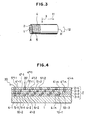
- a multi-layered circuit of superconducting conductors can be constructed as is illustrated in Fig. 4 which represents a fourth embodiment of the invention.
- a first layer 2-1 is first formed with a first superconducting helix 4-1, 4-2, ...4-n in the same manner as described above with reference to Fig. 3.
- a second ceramic layer 2-2 is deposited on top of the first layer 2-1, and this is followed by forming a second superconducting helix 4 ⁇ -1, 4 ⁇ -2, ...4 ⁇ -n as above described.
- the end 4 ⁇ -n of the second helix may be connected with the end 4-n of the first helix by means of a superconductor portion 10-1 making electrical contact with the last winding of the first helix 2-1. Since the irradiation of the second layer 2-2 also causes the upper surface of the first layer 2-1 just below the irradiated portion of the second layer to be heated and melted, therefore the second helix is formed so as not to interfere with the first helix 2-1.
- the forming process of the second superconducting helix 2-2 is then repeated to form third and fourth ceramic layers 2-3 and 2-4 with respective third and fourth superconducting helices which, together with the first and second helices, constitute a continuous superconductor in the form of a multilayer coil.
- One end portion 4′′′-1 of the fourth helix is connected to a wire 30 ⁇ to constitute one terminal of the coil, and the other terminal of the coil is defined by a wire 30 connected to the start end 4-1 of the first helix by way of superconducting regions of the second, third and fourth ceramic layers 2-2, 2-3 and 2-4 which are superimposed upon the end 4-1 of the first helix.
- further ceramic layers provided with superconducting helices may be added so as to form, for example, a device comprising several tens of ceramic layers.
- the superconducting helices are shown connected in series in Fig.4, the helices can if desired be formed without interconnections therebetween, and the superconducting patterns on the ceramic layers can be designed to produce an individual pair of terminals for each helix so that connections among the helices can be arbitrarily arranged as desired.
- the substrate 1 is an insulating disc which is provided with a terminal 6 at its periphery and a terminal 7 at its centre.
- the disc 1 is provided with a sputtered ceramic layer which is then irradiated with a laser beam in the same manner as described above for the first embodiment.
- the disc 1 is turned about its centre while the distance of the point of impingement of the laser beam from the centre is decreased so as to form a superconducting spiral 4 connecting the terminals 6 and 7 on the disc 1.
- Tc was measured to be 27°C.
- a multi-layered structure based upon the Fig. 5 embodiment can be constructed in a manner similar to that of the preceding embodiment, the arrangement comprising discs formed with spirals of opposed senses superposed in turn.
- Fig. 6 is a perspective view showing a sixth embodiment of the present invention.
- a linear laser beam 3 is shown radiated onto a disc 1 on which a ceramic film 2 is deposited having the composition of a superconducting ceramic as explained in the foregoing embodiments.
- the disc 1 is turned around its axis so that the ceramic film 2 is irradiated repeatedly with the laser beam and undergoes annealing and recrystallization.
- A is one or more elements of Group IIIa of the Japanese Periodic Table, e.g the rare earth elements
- A is one or more elements of Group Vb of the Japanese Periodic Table such as Bi, Sb and As
- Examples of this general formula are BiSrCaCuCu20 x and Bi4Sr3Ca3Cu40 x .
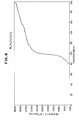
- Tc onset and Tco were measured for samples consistent with the formula Bi4Sr y Ca3Cu40 x (y is around 1.5) and were found to be 40-60°K, which is not particularly high.
- Relatively high critical temperatures were obtained with samples conforming to the stoichiometric formulae Bi4Sr4Ca2Cu40 x and Bi2Sr3Ca2Cu20 x .
- Figs. 7 and 8 are graphical diagrams showing the relationship between the resistivity and the temperature for both samples.
- the numbr x designating the oxygen proportion is 6-10, e.g around 8.1.
- a superconducting pattern can be produced by radiating a laser beam onto a superconducting thin film so that prescribed irradiated portions of the film are converted into non-superconducting material, the superconducting pattern being composed of the non-irradiated portions of the ceramic film which remain superconductive.
- YBCO YBCO
- the Tc of the superconducting film was measured and found to be 85°C. Then a prescribed portion of the superconducting film was irradiated with a laser beam at room temperature so as to convert such portion from a superconducting material to a non-superconducting material. By this process, a superconducting pattern was produced on the film in the areas thereof which had not been irradiated.
- An important feature of this process is that the irradiation is carried out at a relatively low temperature so that the material melted by the irradiation will be rapidly cooled and will resolidify in an agitated and disordered condition which is non-superconductive.
- the ambient temperature during irradiation is thus chosen to be not higher than 100°C in general.
- Other process conditions were the same as for the first embodiment. Of course, such an inverse process can be applied to the second to fourth embodiments in similar manner.
Abstract
Description
- This invention relates to superconducting ceramics and methods for manufacturing the same.
- It has been known to use metallic materials such as Nb3Ge to wind a coil to form a superconducting magnet since such metallic materials have a high ductility and malleability. However such metallic materials do not have a high Tc, and in recent years, superconducting ceramics which have a high Tc have attracted the interest of researchers. However, such superconducting ceramics are fragile and have low ductility and malleability, and therefore it has been quite impossible to form a superconducting coil from a conductor made of such superconducting ceramics.
- It is therefore the object of the present invention to provide a high Tc superconductor in any desired form and to provide a method of manufacturing a high Tc superconductor in any desired form, which method is suitable for mass-production.
- The present invention resides generally in the concept of providing a layer of a prescribed material on a substrate and irradiating the said layer so as, depending upon the original properties of the layer, either to convert it into a superconducting layer in the regions where it is irradiated or to convert it from a superconducting layer in the said regions. The invention takes advantage of the fact that the superconductivity of a material is not only dependent upon its chemical composition but also is dependent upon the orderliness of its structure, and proposes either to render an ordered superconducting structure into a disordered non-superconducting structure or vice-versa by irradiation. Furthermore, by selectively irradiating only specific regions of a structure high Tc superconductors can be formed into coils and other shapes which have hitherto been unobtainable.
- In accordance with an embodiment of the present invention which is described hereinafter, an oxide mixture prescribed for constituting a superconducting ceramic is first deposited in the form of a thin film onto a substrate by sputtering. By making use of sputtering to form the thin film, an amorphous or other structure of the resultant film is obtained which is abundant in lattice defects and/or imperfections so that the resistivity of the ceramic material is rather high. Prescribed portions of the thin film are then irradiated with a laser beam which, for example, scans the surface of the ceramic layer within a constant width, strip-shaped region of the layer. The irradiated portion of the layer is melted and annealed by the laser and recrystallizes as it cools. By virtue of the annealing effect of the laser, the number of lattice defects and imperfections is decreased and the amount of lattice strain is decreased, so that a microcrystalline structure having superconductive properties is obtained only in the irradiated regions whereby a superconducting pattern may be obtained. The recrystallization results furthermore in impurities contained in the ceramic material being redistributed and collected near the surface of the thin film layer so that a high purity superconducting ceramic can be obtained in the thickness of the thin film.
- The sputtered ceramic material may for example be such as those represented by the formulae (Y1-xBax)₂Cu0₄, hereinafter called YBCO, where x = 0.01 to 0.1 and preferably 0.05 to 0.1, (La1-xBax)₂Cu0₄, hereinafter called BLCO where x = 0.01 to 0.1 and preferably 0.05 to 0.1, (La1-xSrx)₂Cu0₄, hereinafter called SLCO, where x = 0.01 to 0.1 and preferably 0.05 to 0.1, and (La1-xAx)₂Cu0₄, where A represents an element in Group IIa of the Japanese Periodic Table and where x = 0.01 to 0.1 and preferably 0.05 to 0.1. The irradiation of the ceramic layer may be carried out in an oxidizing atmosphere, in which case the proportions of the above composition may be decreased correspondingly so that the desired stoichiometry are obtained taking account of oxidation of the irradiated thin film portions.
- Those parts of the thin film layer intervening between neighbouring superconducting portions function as insulators which isolate the superconducting portion from its surroundings and also provide the resulting superconducting device with an even upper surface which enables multi-layered structures to be formed.
- This isolating effect is advantageous in view of the fact that in the prior art the characteristics of superconducting ceramics have tended to be influenced by the material which is in contact with the ceramics in the structure of the superconducting device. For instance, when a substrate made of silicon oxide or silicon nitride has been used, acid-base reactions have been known to occur between the substrate and an oxide superconducting ceramic layer formed thereon.
- As will be appreciated from consideration of the following descriptions, the present invention enables superconductors to be formed in various shapes by a method which is very simple as compared to photolithography so that the present invention can be particularly effective when applied to mass-production manufacturing.
- Further features of the invention are set forth with particularity in the appended claims and will become apparent to those possesssed with the relevant skills from consideration of the following description, given with reference to the accompanying drawings, of exemplary embodiments of the invention.
-
- Figs. 1(A) to 1(C) are side views illustrating a first exemplary manufacturing process in accordance with the present invention;
- Figs. 2(A) to 2(C) are side views illustrating a second exemplary manufacturing process in accordance with the present invention;
- Fig. 3 is a perspective view illustrating a third exemplary manufacturing process in accordance with the present invention;
- Fig. 4 is a cross sectional view illustrating a fourth exemplary manufacturing process in accordance with the present invention;
- Fig. 5 is a perspective view illustrating a fifth exemplary manufacturing process in accordance with the present invention;
- Fig. 6 is a perspective view illustrating a sixth exemplary manufacturing process in accordance with the present invention; and
- Figs. 7 and 8 are graphical diagrams showing the relationship between the resistivity and the temperature of superconducting oxide ceramics manufactured in accordance with the present invention.
- For the avoidance of doubt it is to be noted that all references herein and in the appended claims to the Periodic Table and to specific Groups of the Periodic Table are to be understood to refer to the Japanese Periodic Table and to the Groups thereof as described in the Iwanami "Physics and Chemistry Dictionary". As compared with the Group designations of the Periodic Table as described in "The Penguin Dictionary of Science" for example, which are the Group designations commonly accepted throughout Europe, Groups Ia, IIa, VIII, Ib, IIb and 0 are the same in the Japanese and European Periodic Tables, Groups IIIa, IVa, Va, VIa and VIIa of the Japanese Periodic Table correspond respectively to Groups IIIb, IVb, Vb, VIb and VIIb of the European Periodic Table, and Groups IIIb, IVb, Vb, VIb and VIIb of the Japanese Periodic Table correspond respectively to Groups IIIa, IVa, Va, VIa and VIIa of the European Periodic Table.
- Referring to Figs. 1(A) to (C), a manufacturing process in accordance with the present invention will be described. In Fig. 1(A), a
substrate 1 may be made of a ceramic material such as alumina, silicon oxide, aluminium nitride, zirconia, yttria or USZ(yttria stabilized zircon), or may be made of metal or of glass. YSZ, yttria or zirconia are particularly suitable having regard to the desirability of matching the coefficient of thermal expansion of the substrate to that of the superconducting layer formed thereon as hereinafter described. The differential coefficient of thermal expansion between the underlying substrate and the overlying ceramic thin film should be as small as possible and preferably within 50% of the thermal expansion coefficient of the ceramic thin film, since if the substrate and the ceramic thin film have substantially different thermal expansion coefficients, then strain developed between them may hinder the formation of a superconducting structure by recrystallization of the ceramic film. - A ceramic film of BLCO of 0.5 to 20 microns thickness, e.g. 2 microns, is formed on the
substrate 1 by sputtering as is illustrated in Fig.1(B). The sputtering is carried out with a target mixture conforming to the formula (La1-xBax)₂Cu0₄, where x=0.075 for example. During the sputtering, thesubstrate 1 is placed in an atmosphere of argon to which a small amount of oxygen is added, and the sputtering is effected at a temperature of from room temperature to 400°C, e.g. 250°C. - Having formed the
ceramic film 2 by sputtering, the next step as shown in Fig. 1(C) is to irradiate the ceramic thin film using a series oflaser beam pulses 3 of 1.06 microns wavelength derived by means of a YAG laser. Each laser pulse is radiated to a circular spot described on the film which shares a 60-80% area with the irradiating spot for the preceding pulse (and also of the subsequent pulse). The laser beam is scanned across the ceramic film at a scanning speed of 2m/min. The pulse frequency is from 5 to 30 KHz, e.g. 8 KHz. The spot diameter is 50 microns. By virtue of this irradiation, the irradiated portions of the ceramic film are melted and then recrystallized. The whole substrate is heated during the laser processing to around 300-800°C, e.g. 600°C, by means of a halogen lamp. By providing this high temperature environment, it is ensured that the film does not crack as as result of too rapid cooling to room temperature from the temperature of 1300°C or higher which is momentarily experienced at the irradiated portion. - As a result of the process illustrated in Figs. 1(A) to 1(C) and described above, a superconductor is fabricated in the form of a plurality of
strips 4 positioned on thefilm 2 with intervals therebetween. The Tc of thestrips 4 was measured to be 29°C. - In a modification of the foregoing embodiment, an excimer laser (Kr, KrC1 for example) may be used instead of the YAG laser, and a strip portion of the ceramic layer of from 5-100 microns wide can be irradiated in a single operation using a linear laser beam derived by squezing with an optical system a pulsed laser beam having a 20 × 30 mm² cross-sectional area. Also, the first embodiment can be carried out making use of a pulsed laser beam emitted from an excimer laser (wavelength =0.25 micron). In this case, the pulse frequency is chosen at about 100KHz which causes the prescribed irradiated portions of the ceramic film to be heated momentarily to about 1000°C or higher. Other manufacturing conditions for carrying out the process using an excimer laser are the same as for the process with a YAG laser. Since the power of an excimer laser is relatively high, the ceramic layer can be oxidized in an oxidizing atmosphere by the irradiation so that, for depositing the ceramic film, a sputtering target comprising (La1-xBax)₂Cu04-d may be used, where d is a compensatory factor for cancelling out the oxygen increment due to laser annealing of the ceramic in an oxidizing atmosphere, and x=0.075 for example. According to experiments, conducted with the process of Figs. 1(A) to 1(C) thus a Tc of 43°K was obtained for the resultant superconductor.
- Fig. 2 shows a second embodiment of the invention. In this embodiment, substantially the same procedure is repeated as for the preceding embodiment except as described below. A
substrate 1 is irradiated with pulses having an elongated rectangular cross-section which are emitted from an excimer laser of 0.25 micron wavelength. The irradiation site on thesubstrate 1 is shifted continuously as shown in Fig. 2(C) in such a way that the region irradiated by each pulse is superimposed on 80-98% of the preceding pulse. The scanning speed is 2cm/min. The pulse frequency is 100KHz. The beam cross-section is 50 microns thick and 10cm wide. By means of this process, a superconducting band region can be formed of 10cm width, for example. - Fig. 3 shows a third embodiment of the invention. In this embodiment, substantially the same procedure is repeated as for the first embodiment except as described below. The
substrate 1 is a cylinder. On the substrate surface there is deposited aceramic film 2 by effecting sputtering while thesubstrate 1 is rotating in the direction indicated by thearrow 12. After completion of the film, a laser beam irradiates the substrate. The position of impingement of the laser beam is shifted in the axial direction of thecylinder 1 while thesubstrate 1 is rotating around its axis. By this process, a continuoushelical superconductor 4 can be formed on thecylinder 1 with each part of the helix isolated from its adjacent parts by the intervening non-superconductingceramic film 5 which has not been irradiated. - By repeating the above process described with reference to Fig. 3, a multi-layered circuit of superconducting conductors can be constructed as is illustrated in Fig. 4 which represents a fourth embodiment of the invention. As shown in Fig. 4, a first layer 2-1 is first formed with a first superconducting helix 4-1, 4-2, ...4-n in the same manner as described above with reference to Fig. 3. Then, on top of the first layer 2-1 there is deposited a second ceramic layer 2-2, and this is followed by forming a second superconducting helix 4ʹ-1, 4ʹ-2, ...4ʹ-n as above described. The end 4ʹ-n of the second helix may be connected with the end 4-n of the first helix by means of a superconductor portion 10-1 making electrical contact with the last winding of the first helix 2-1. Since the irradiation of the second layer 2-2 also causes the upper surface of the first layer 2-1 just below the irradiated portion of the second layer to be heated and melted, therefore the second helix is formed so as not to interfere with the first helix 2-1. The forming process of the second superconducting helix 2-2 is then repeated to form third and fourth ceramic layers 2-3 and 2-4 with respective third and fourth superconducting helices which, together with the first and second helices, constitute a continuous superconductor in the form of a multilayer coil. One
end portion 4‴-1 of the fourth helix is connected to a wire 30ʹ to constitute one terminal of the coil, and the other terminal of the coil is defined by awire 30 connected to the start end 4-1 of the first helix by way of superconducting regions of the second, third and fourth ceramic layers 2-2, 2-3 and 2-4 which are superimposed upon the end 4-1 of the first helix. If a coil having a larger number of turns is required, further ceramic layers provided with superconducting helices may be added so as to form, for example, a device comprising several tens of ceramic layers. - Although the superconducting helices are shown connected in series in Fig.4, the helices can if desired be formed without interconnections therebetween, and the superconducting patterns on the ceramic layers can be designed to produce an individual pair of terminals for each helix so that connections among the helices can be arbitrarily arranged as desired.
- In Fig. 5 there is illustrated a fifth embodiment of the present invention. In this embodiment, the
substrate 1 is an insulating disc which is provided with aterminal 6 at its periphery and aterminal 7 at its centre. Thedisc 1 is provided with a sputtered ceramic layer which is then irradiated with a laser beam in the same manner as described above for the first embodiment. Duringirradiation 3, thedisc 1 is turned about its centre while the distance of the point of impingement of the laser beam from the centre is decreased so as to form asuperconducting spiral 4 connecting theterminals disc 1. According to experimental results that have been obtained Tc was measured to be 27°C. A multi-layered structure based upon the Fig. 5 embodiment can be constructed in a manner similar to that of the preceding embodiment, the arrangement comprising discs formed with spirals of opposed senses superposed in turn. - Fig. 6 is a perspective view showing a sixth embodiment of the present invention. In the figure, a
linear laser beam 3 is shown radiated onto adisc 1 on which aceramic film 2 is deposited having the composition of a superconducting ceramic as explained in the foregoing embodiments. During irradiation with the laser beam, thedisc 1 is turned around its axis so that theceramic film 2 is irradiated repeatedly with the laser beam and undergoes annealing and recrystallization. - Superconducting ceramics in accordance with the present invention also may be prepared in accordance with the stoichiometric formulae (A1-xBx)y
Cu z0w, where A is one or more elements of Group IIIa of the Japanese Periodic Table, e.g the rare earth elements, B is one or more elements of Group IIa of the Japanese Periodic Table, e.g. the alkaline earth metals including beryllium and magnesium, and x=0-1; y=2.0-4.0, preferably 2.5-3.5; z=1.0-4.0, preferably 1.5-3.5; and w=4.0-10.0, preferably 6.0-8.0. Also, superconducting ceramics in accordance with the present invention may be prepared in accordance with the stoichiometric formulae (A1-xBx)yCu z0w, where A is one or more elements of Group Vb of the Japanese Periodic Table such as Bi, Sb and As, B is one or more elements of Group IIa of the Japanese Periodic Table, e.g. the alkaline earth metals including beryllium and magnesium, and x=0.3-1; y=2.0-4.0, preferably 2.5-3.5; z=1.0-4.0, preferably 1.5-3.5; and w=4.0-10.0, preferably 6.0-8.0. Examples of this general formula are BiSrCaCuCu₂0x and Bi₄Sr₃Ca₃Cu₄0x. Tc onset and Tco were measured for samples consistent with the formula Bi₄SryCa₃Cu₄0x (y is around 1.5) and were found to be 40-60°K, which is not particularly high. Relatively high critical temperatures were obtained with samples conforming to the stoichiometric formulae Bi₄Sr₄Ca₂Cu₄0x and Bi₂Sr₃Ca₂Cu₂0x. Figs. 7 and 8 are graphical diagrams showing the relationship between the resistivity and the temperature for both samples. The numbr x designating the oxygen proportion is 6-10, e.g around 8.1. - Hereinbefore, descriptions have been made of embodiments in which non-superconducting materials are converted to superconducting materials by irradiation. However, in accordance with the present invention, the inverse process is possible. Namely, a superconducting pattern can be produced by radiating a laser beam onto a superconducting thin film so that prescribed irradiated portions of the film are converted into non-superconducting material, the superconducting pattern being composed of the non-irradiated portions of the ceramic film which remain superconductive. Experiments using this inverse process were made using YBCO. After depositing a thin film of YBCO upon a substrate by sputtering, the whole film was fired at 600-900°C so as to make the film superconducting. The Tc of the superconducting film was measured and found to be 85°C. Then a prescribed portion of the superconducting film was irradiated with a laser beam at room temperature so as to convert such portion from a superconducting material to a non-superconducting material. By this process, a superconducting pattern was produced on the film in the areas thereof which had not been irradiated. An important feature of this process is that the irradiation is carried out at a relatively low temperature so that the material melted by the irradiation will be rapidly cooled and will resolidify in an agitated and disordered condition which is non-superconductive. The ambient temperature during irradiation is thus chosen to be not higher than 100°C in general. Other process conditions were the same as for the first embodiment. Of course, such an inverse process can be applied to the second to fourth embodiments in similar manner.
- While the above description has been made with reference to several specific embodiments, it is to be understood that the present invention is limited only by the appended claims and is not limited to the particular examples described.
Claims (29)
forming a non-superconducting layer on a surface, the chemical composition of said layer being substantially consistent with that of a superconducting ceramic; and
irradiating at least a portion of said layer with light so as to melt the irradiated portion and permitting the melted portion to resolidify in a superconducting configuration, the irradiation of the non-superconducting layer serving to convert the irradiated portion into a superconducting material.
forming a non-superconducting layer on a surface, the composition of said layer being so prescribed that said layer is capable of being converted to a superconducting ceramic material when irradiated, melted and recrystallized; and
irradiating and melting at least a portion of said layer with light and permitting the irradiated portion to recrystallize whereby said irradiated portion is converted from non-superconducting material to superconducting ceramic material.
forming a superconducting ceramic layer on a surface; and
irradiating and melting a portion of said ceramic layer with light to convert the irradiated portion from a superconducting material to a non-superconducting material when cooled.
Applications Claiming Priority (6)
| Application Number | Priority Date | Filing Date | Title |
|---|---|---|---|
| JP58466/87 | 1987-03-12 | ||
| JP62058466A JP2645489B2 (en) | 1987-03-12 | 1987-03-12 | Superconductor fabrication method |
| JP284627/87 | 1987-11-11 | ||
| JP62284628A JPH07114296B2 (en) | 1987-11-11 | 1987-11-11 | Superconductor |
| JP284628/87 | 1987-11-11 | ||
| JP62284627A JPH07114295B2 (en) | 1987-11-11 | 1987-11-11 | Superconducting coil fabrication method |
Publications (3)
| Publication Number | Publication Date |
|---|---|
| EP0282360A2 true EP0282360A2 (en) | 1988-09-14 |
| EP0282360A3 EP0282360A3 (en) | 1990-05-23 |
| EP0282360B1 EP0282360B1 (en) | 1995-11-02 |
Family
ID=27296593
Family Applications (1)
| Application Number | Title | Priority Date | Filing Date |
|---|---|---|---|
| EP88302227A Expired - Lifetime EP0282360B1 (en) | 1987-03-12 | 1988-03-14 | Method for manufacturing components of superconducting ceramic oxide materials |
Country Status (2)
| Country | Link |
|---|---|
| EP (1) | EP0282360B1 (en) |
| DE (1) | DE3854626T2 (en) |
Cited By (12)
| Publication number | Priority date | Publication date | Assignee | Title |
|---|---|---|---|---|
| EP0285106A2 (en) * | 1987-03-30 | 1988-10-05 | Sumitomo Electric Industries Limited | Method of forming superconducting circuit |
| EP0286106A2 (en) * | 1987-04-08 | 1988-10-12 | Hitachi, Ltd. | Process for manufacturing a superconductive device |
| EP0290357A2 (en) * | 1987-05-04 | 1988-11-09 | EASTMAN KODAK COMPANY (a New Jersey corporation) | Process for the preparation of copper oxide ceramic superconductive articles, and process for their preparation |
| EP0304807A2 (en) * | 1987-08-22 | 1989-03-01 | Sumitomo Electric Industries Limited | Method for producing superconducting circuit |
| EP0311331A2 (en) * | 1987-10-07 | 1989-04-12 | United Kingdom Atomic Energy Authority | Superconducting ceramic circuit elements |
| FR2647266A1 (en) * | 1989-05-17 | 1990-11-23 | Ecole Cle Arts Manufactures | Electrical or electronic circuit element including a super-conductor to which conducting elements are fixed |
| US5143894A (en) * | 1987-10-14 | 1992-09-01 | Mordechai Rothschild | Formation and high resolution patterning of superconductors |
| US5194419A (en) * | 1989-07-25 | 1993-03-16 | The Furukawa Electric Co., Ltd. | Method for manufacturing an oxide superconductive multilayer circuit |
| US5229360A (en) * | 1989-07-24 | 1993-07-20 | The Furukawa Electric Co., Ltd. | Method for forming a multilayer superconducting circuit |
| EP0662724A2 (en) * | 1987-03-18 | 1995-07-12 | International Business Machines Corporation | Films of high Tc oxide superconductors |
| US7112556B1 (en) | 1987-03-25 | 2006-09-26 | Semiconductor Energy Laboratory Co., Ltd. | Superconducting ceramics |
| CN100487937C (en) * | 2007-01-29 | 2009-05-13 | 中国科学院等离子体物理研究所 | Low heat conductive elastic support body of super low temperature part |
Families Citing this family (1)
| Publication number | Priority date | Publication date | Assignee | Title |
|---|---|---|---|---|
| US8852959B2 (en) * | 2011-12-19 | 2014-10-07 | Northrup Grumman Systems Corporation | Low temperature resistor for superconductor circuits |
Citations (5)
| Publication number | Priority date | Publication date | Assignee | Title |
|---|---|---|---|---|
| EP0202895A2 (en) * | 1985-05-16 | 1986-11-26 | Kabushiki Kaisha Toshiba | Method of manufacturing compound superconductors |
| EP0285106A2 (en) * | 1987-03-30 | 1988-10-05 | Sumitomo Electric Industries Limited | Method of forming superconducting circuit |
| EP0286106A2 (en) * | 1987-04-08 | 1988-10-12 | Hitachi, Ltd. | Process for manufacturing a superconductive device |
| WO1988010011A1 (en) * | 1987-06-12 | 1988-12-15 | Siemens Aktiengesellschaft | Process for manufacturing conductive regions from an oxide-ceramic superconducting material having a high conductivity-change temperature |
| DE3815185A1 (en) * | 1987-08-05 | 1989-02-16 | Siemens Ag | Method for producing a hybrid pattern containing semiconducting and superconducting material |
-
1988
- 1988-03-14 DE DE3854626T patent/DE3854626T2/en not_active Expired - Fee Related
- 1988-03-14 EP EP88302227A patent/EP0282360B1/en not_active Expired - Lifetime
Patent Citations (5)
| Publication number | Priority date | Publication date | Assignee | Title |
|---|---|---|---|---|
| EP0202895A2 (en) * | 1985-05-16 | 1986-11-26 | Kabushiki Kaisha Toshiba | Method of manufacturing compound superconductors |
| EP0285106A2 (en) * | 1987-03-30 | 1988-10-05 | Sumitomo Electric Industries Limited | Method of forming superconducting circuit |
| EP0286106A2 (en) * | 1987-04-08 | 1988-10-12 | Hitachi, Ltd. | Process for manufacturing a superconductive device |
| WO1988010011A1 (en) * | 1987-06-12 | 1988-12-15 | Siemens Aktiengesellschaft | Process for manufacturing conductive regions from an oxide-ceramic superconducting material having a high conductivity-change temperature |
| DE3815185A1 (en) * | 1987-08-05 | 1989-02-16 | Siemens Ag | Method for producing a hybrid pattern containing semiconducting and superconducting material |
Non-Patent Citations (2)
| Title |
|---|
| J. APPL. PHYS., vol. 52, no. 8, August 1981, pages 5107-5111, American Institute of Physics; Y. MATSUI et al.: "Laser annealing to produce ferroelectric-hase PbTiO3 thin films". * |
| JAPANESE JOURNAL OF APPLIED PHYSICS, vol. 27, no. 2, February 1988, pages L231-L233, Part 2, New York, US; N. AIZAKI et al.: "YBa2Cu3Oy super-conducting thin film obtained by laser annealing" * |
Cited By (18)
| Publication number | Priority date | Publication date | Assignee | Title |
|---|---|---|---|---|
| EP0662724A3 (en) * | 1987-03-18 | 1995-08-09 | Ibm | |
| EP0662724A2 (en) * | 1987-03-18 | 1995-07-12 | International Business Machines Corporation | Films of high Tc oxide superconductors |
| US7112556B1 (en) | 1987-03-25 | 2006-09-26 | Semiconductor Energy Laboratory Co., Ltd. | Superconducting ceramics |
| EP0285106A2 (en) * | 1987-03-30 | 1988-10-05 | Sumitomo Electric Industries Limited | Method of forming superconducting circuit |
| EP0285106A3 (en) * | 1987-03-30 | 1989-08-23 | Sumitomo Electric Industries Limited | Method of forming superconducting circuit |
| EP0286106A2 (en) * | 1987-04-08 | 1988-10-12 | Hitachi, Ltd. | Process for manufacturing a superconductive device |
| EP0286106B1 (en) * | 1987-04-08 | 1995-08-02 | Hitachi, Ltd. | Process for manufacturing a superconductive device |
| EP0290357B1 (en) * | 1987-05-04 | 1993-09-01 | EASTMAN KODAK COMPANY (a New Jersey corporation) | Process for the preparation of copper oxide ceramic superconductive articles, and process for their preparation |
| EP0290357A2 (en) * | 1987-05-04 | 1988-11-09 | EASTMAN KODAK COMPANY (a New Jersey corporation) | Process for the preparation of copper oxide ceramic superconductive articles, and process for their preparation |
| EP0304807A2 (en) * | 1987-08-22 | 1989-03-01 | Sumitomo Electric Industries Limited | Method for producing superconducting circuit |
| EP0304807A3 (en) * | 1987-08-22 | 1990-03-21 | Sumitomo Electric Industries, Limited | Method for producing superconducting circuit |
| EP0311331A2 (en) * | 1987-10-07 | 1989-04-12 | United Kingdom Atomic Energy Authority | Superconducting ceramic circuit elements |
| EP0311331A3 (en) * | 1987-10-07 | 1990-02-14 | United Kingdom Atomic Energy Authority | Superconducting ceramic circuit elements |
| US5143894A (en) * | 1987-10-14 | 1992-09-01 | Mordechai Rothschild | Formation and high resolution patterning of superconductors |
| FR2647266A1 (en) * | 1989-05-17 | 1990-11-23 | Ecole Cle Arts Manufactures | Electrical or electronic circuit element including a super-conductor to which conducting elements are fixed |
| US5229360A (en) * | 1989-07-24 | 1993-07-20 | The Furukawa Electric Co., Ltd. | Method for forming a multilayer superconducting circuit |
| US5194419A (en) * | 1989-07-25 | 1993-03-16 | The Furukawa Electric Co., Ltd. | Method for manufacturing an oxide superconductive multilayer circuit |
| CN100487937C (en) * | 2007-01-29 | 2009-05-13 | 中国科学院等离子体物理研究所 | Low heat conductive elastic support body of super low temperature part |
Also Published As
| Publication number | Publication date |
|---|---|
| DE3854626D1 (en) | 1995-12-07 |
| DE3854626T2 (en) | 1996-07-04 |
| EP0282360A3 (en) | 1990-05-23 |
| EP0282360B1 (en) | 1995-11-02 |
Similar Documents
| Publication | Publication Date | Title |
|---|---|---|
| KR910004993B1 (en) | Method of manufacturing a superconducting pattern by light irradiation | |
| EP0306287B1 (en) | Superconducting ceramic circuits and manufacturing method for the same | |
| EP0282360A2 (en) | Method for manufacturing components of superconducting ceramic oxide materials | |
| US5232908A (en) | Method of manufacturing an oxide superconductor/metal laminate | |
| EP0292387A2 (en) | Method for producing a superconducting circuit | |
| US5318948A (en) | Oxide superconductor, superconducting wire and coil using the same and method of production thereof | |
| EP0410373B1 (en) | Method for forming a superconducting circuit | |
| US5225394A (en) | Method for manufacturing high Tc superconducting circuits | |
| US6272730B1 (en) | Process for producing a multifilamentary superconducting tape | |
| US5168259A (en) | Superconducting coil | |
| US5248658A (en) | Method of manufacturing a superconducting oxide pattern by laser sublimation | |
| JPS63207007A (en) | Superconductor | |
| JPS63224117A (en) | Manufacture of superconductor | |
| EP0380318B1 (en) | Process for making superconducting wires | |
| JPS63207009A (en) | Manufacture of superconductor | |
| EP0291034A2 (en) | Method for producing oxide superconductor | |
| Solovyov et al. | Electromechanical properties of 1-mm-wide superconducting cables comprised of exfoliated YBCO filaments | |
| JP2630362B2 (en) | Superconducting coil | |
| JPH0812819B2 (en) | Superconductor fabrication method | |
| JPH0362905A (en) | Manufacture of superconducting coil | |
| KR20020064040A (en) | Cu-Sheathed Bi2Sr2CaCu2Ox High-Tc Superconductor Thick Film and Method for Producing the same | |
| JPS63224270A (en) | Manufacture of superconductor device | |
| JPH07114296B2 (en) | Superconductor | |
| JP2585624B2 (en) | Superconducting coil fabrication method | |
| JP2754494B2 (en) | Method for producing an oriented layer of Bi-Sr-Ca-Cu-oxide or T1-Ba-Ca-Cu-oxide high temperature superconductor |
Legal Events
| Date | Code | Title | Description |
|---|---|---|---|
| PUAI | Public reference made under article 153(3) epc to a published international application that has entered the european phase |
Free format text: ORIGINAL CODE: 0009012 |
|
| AK | Designated contracting states |
Kind code of ref document: A2 Designated state(s): DE FR GB |
|
| PUAL | Search report despatched |
Free format text: ORIGINAL CODE: 0009013 |
|
| AK | Designated contracting states |
Kind code of ref document: A3 Designated state(s): DE FR GB |
|
| 17P | Request for examination filed |
Effective date: 19901107 |
|
| 17Q | First examination report despatched |
Effective date: 19920707 |
|
| GRAA | (expected) grant |
Free format text: ORIGINAL CODE: 0009210 |
|
| AK | Designated contracting states |
Kind code of ref document: B1 Designated state(s): DE FR GB |
|
| REF | Corresponds to: |
Ref document number: 3854626 Country of ref document: DE Date of ref document: 19951207 |
|
| ET | Fr: translation filed | ||
| PGFP | Annual fee paid to national office [announced via postgrant information from national office to epo] |
Ref country code: FR Payment date: 19960126 Year of fee payment: 9 |
|
| PGFP | Annual fee paid to national office [announced via postgrant information from national office to epo] |
Ref country code: GB Payment date: 19960305 Year of fee payment: 9 |
|
| PGFP | Annual fee paid to national office [announced via postgrant information from national office to epo] |
Ref country code: DE Payment date: 19960313 Year of fee payment: 9 |
|
| PLBE | No opposition filed within time limit |
Free format text: ORIGINAL CODE: 0009261 |
|
| STAA | Information on the status of an ep patent application or granted ep patent |
Free format text: STATUS: NO OPPOSITION FILED WITHIN TIME LIMIT |
|
| 26N | No opposition filed | ||
| PG25 | Lapsed in a contracting state [announced via postgrant information from national office to epo] |
Ref country code: GB Effective date: 19970314 |
|
| GBPC | Gb: european patent ceased through non-payment of renewal fee |
Effective date: 19970314 |
|
| PG25 | Lapsed in a contracting state [announced via postgrant information from national office to epo] |
Ref country code: FR Free format text: LAPSE BECAUSE OF NON-PAYMENT OF DUE FEES Effective date: 19971128 |
|
| PG25 | Lapsed in a contracting state [announced via postgrant information from national office to epo] |
Ref country code: DE Effective date: 19971202 |
|
| REG | Reference to a national code |
Ref country code: FR Ref legal event code: ST |