EP0286106A2 - Process for manufacturing a superconductive device - Google Patents
Process for manufacturing a superconductive device Download PDFInfo
- Publication number
- EP0286106A2 EP0286106A2 EP88105573A EP88105573A EP0286106A2 EP 0286106 A2 EP0286106 A2 EP 0286106A2 EP 88105573 A EP88105573 A EP 88105573A EP 88105573 A EP88105573 A EP 88105573A EP 0286106 A2 EP0286106 A2 EP 0286106A2
- Authority
- EP
- European Patent Office
- Prior art keywords
- superconductive
- oxide
- oxygen
- layer
- oxides
- Prior art date
- Legal status (The legal status is an assumption and is not a legal conclusion. Google has not performed a legal analysis and makes no representation as to the accuracy of the status listed.)
- Granted
Links
Images


Classifications
-
- H—ELECTRICITY
- H01—ELECTRIC ELEMENTS
- H01B—CABLES; CONDUCTORS; INSULATORS; SELECTION OF MATERIALS FOR THEIR CONDUCTIVE, INSULATING OR DIELECTRIC PROPERTIES
- H01B12/00—Superconductive or hyperconductive conductors, cables, or transmission lines
-
- H—ELECTRICITY
- H01—ELECTRIC ELEMENTS
- H01F—MAGNETS; INDUCTANCES; TRANSFORMERS; SELECTION OF MATERIALS FOR THEIR MAGNETIC PROPERTIES
- H01F41/00—Apparatus or processes specially adapted for manufacturing or assembling magnets, inductances or transformers; Apparatus or processes specially adapted for manufacturing materials characterised by their magnetic properties
- H01F41/02—Apparatus or processes specially adapted for manufacturing or assembling magnets, inductances or transformers; Apparatus or processes specially adapted for manufacturing materials characterised by their magnetic properties for manufacturing cores, coils, or magnets
- H01F41/04—Apparatus or processes specially adapted for manufacturing or assembling magnets, inductances or transformers; Apparatus or processes specially adapted for manufacturing materials characterised by their magnetic properties for manufacturing cores, coils, or magnets for manufacturing coils
- H01F41/048—Superconductive coils
-
- H—ELECTRICITY
- H01—ELECTRIC ELEMENTS
- H01F—MAGNETS; INDUCTANCES; TRANSFORMERS; SELECTION OF MATERIALS FOR THEIR MAGNETIC PROPERTIES
- H01F6/00—Superconducting magnets; Superconducting coils
- H01F6/06—Coils, e.g. winding, insulating, terminating or casing arrangements therefor
-
- H—ELECTRICITY
- H10—SEMICONDUCTOR DEVICES; ELECTRIC SOLID-STATE DEVICES NOT OTHERWISE PROVIDED FOR
- H10N—ELECTRIC SOLID-STATE DEVICES NOT OTHERWISE PROVIDED FOR
- H10N60/00—Superconducting devices
- H10N60/01—Manufacture or treatment
- H10N60/0268—Manufacture or treatment of devices comprising copper oxide
- H10N60/0661—After-treatment, e.g. patterning
-
- H—ELECTRICITY
- H10—SEMICONDUCTOR DEVICES; ELECTRIC SOLID-STATE DEVICES NOT OTHERWISE PROVIDED FOR
- H10N—ELECTRIC SOLID-STATE DEVICES NOT OTHERWISE PROVIDED FOR
- H10N60/00—Superconducting devices
- H10N60/01—Manufacture or treatment
- H10N60/0884—Treatment of superconductor layers by irradiation, e.g. ion-beam, electron-beam, laser beam, X-rays
-
- H—ELECTRICITY
- H10—SEMICONDUCTOR DEVICES; ELECTRIC SOLID-STATE DEVICES NOT OTHERWISE PROVIDED FOR
- H10N—ELECTRIC SOLID-STATE DEVICES NOT OTHERWISE PROVIDED FOR
- H10N60/00—Superconducting devices
- H10N60/20—Permanent superconducting devices
- H10N60/203—Permanent superconducting devices comprising high-Tc ceramic materials
-
- H—ELECTRICITY
- H10—SEMICONDUCTOR DEVICES; ELECTRIC SOLID-STATE DEVICES NOT OTHERWISE PROVIDED FOR
- H10N—ELECTRIC SOLID-STATE DEVICES NOT OTHERWISE PROVIDED FOR
- H10N60/00—Superconducting devices
- H10N60/01—Manufacture or treatment
- H10N60/0912—Manufacture or treatment of Josephson-effect devices
- H10N60/0941—Manufacture or treatment of Josephson-effect devices comprising high-Tc ceramic materials
-
- Y—GENERAL TAGGING OF NEW TECHNOLOGICAL DEVELOPMENTS; GENERAL TAGGING OF CROSS-SECTIONAL TECHNOLOGIES SPANNING OVER SEVERAL SECTIONS OF THE IPC; TECHNICAL SUBJECTS COVERED BY FORMER USPC CROSS-REFERENCE ART COLLECTIONS [XRACs] AND DIGESTS
- Y10—TECHNICAL SUBJECTS COVERED BY FORMER USPC
- Y10S—TECHNICAL SUBJECTS COVERED BY FORMER USPC CROSS-REFERENCE ART COLLECTIONS [XRACs] AND DIGESTS
- Y10S505/00—Superconductor technology: apparatus, material, process
- Y10S505/725—Process of making or treating high tc, above 30 k, superconducting shaped material, article, or device
- Y10S505/73—Vacuum treating or coating
Definitions
- Pellet samples of a non-superconductive YBa2Cu3O 6.2 with 25 mm in length, 6 mm in width and 3 mm in thickness were prepared by the oxide-mixing method.
- Fig. 18 is a graph showing a change of the critical temperature of the samples, as carbonic acid gas laser or electron beam is applied to the samples, with respect to the energy density applied.
- the electron beam was applied at a range of 50 to 100 keV. In both the cases of applying the electron beam and the carbonic acid gas laser, the similar results were obtained.
- the transformation from the non-superconductive form to the superconductive form began to occur at an energy density of about 1 ⁇ 102 J/cm2.
- the superconductor 13 may be used as wiring of circuits.
Abstract
Description
- This invention relates to a process for controlling the oxygen content of a perovskite oxide, layer perovskite oxide, oxygen-dificient layer perovskite oxide, multilayer perovskite oxide and spinel oxide, thereby providing a superconductive oxide having a critical temperature and/or critical current density, and further to a superconductive device and a process for producing the device.
- Hitherto, only three kinds of superconductive alloys such as Nb₃Sn have used for practical applications and their critical temperature exhibiting the superconductivity was at most 23°K for Nb₃Ge. Therefore, expensive helium must be used for cooling the superconductive alloys and cooling efficiency is low. For raising up the cooling efficiency, a material exhibiting superconductivity at a higher temperature has been required. Thus, many and intensive studies on various elements, alloys, compounds, ceramics or organic materials have recently been made. Among these materials, it has recently been discovered that perovskite oxides, particularly layer perovskite oxides have a very high critical temperature Tc. For example, the layer perovskide oxide of a La-Ba-Cu-O, La-Sr-Cu-O or Y-Ba-C-O type has a Tc of 30°K or higher, particularly the Y-Ba-Cu-O type oxide has a Tc of 90°K or higher. Therefore, cheaper liquid hydrogen, liquid neon or liquid nitrogen (one-tenth of the price of liquid helium) can not only be used as a coolant, but also allows their cooling efficiency to be raised up to 20 times that of liquid helium. These superconductive oxides are disclosed in, for example, Physical Review Letters, Vol. 58, No. 4, 1987, pp. 405-407 for the La-Ba-Cu-O type oxides, Physical Review Letters, Vol. 58, No. 4, 1987, pp. 408-410 for the La-Sr-Cu-O type oxides, and NIHON KEIZAI SHIMBUN, Science Column, March 3, 1987 for the Y-Ba-Cu-O type oxides.
- These oxides can be prepared from constituents of the oxides by a so-called sintering method. In this method, it is easy to control the proportions of the constituents other than oxygen but hard to control the proportion of oxygen. Particularly, the oxides sintered under the specified conditions of sintering temperature and sintering time alone have a different critical temperature Tc for each of sintered charges. Tc of sintered oxides varies depending upon oxygen partial pressures of sintering atmospheres, even if the oxides are fired at the same temperature for the same period of time. Such great differences in Tc are caused by differences in oxygen concentration between sintered charges. The oxygen concentration of sintered oxides cannot be controlled even by various post-heat treatments. Therefore, prior art has such a problem that high Tc cannot be obtained with good reproducibility. Accordingly, practical and reliable devices utilizing superconductive oxides have not yet been obtained with good reproducibility.
- Under the circumstances, some processes for controlling the oxygen content of superconductive oxides have been proposed. Processes for controlling the oxygen content to raise up Tc are described in Z. Phy. B-Condensed Matter 67 (1987), p.507, and Extended Abstracts (The 48th Autumn Meeting, 1987), The Japan Society of Applied Physics, No. 1, p.83. In the former, it is shown that O⁺ of 300 keV was applied at a dose of 5 × 10¹⁶ O⁺/cm² to a La-Sr-Cu-O oxides (a film prepared by RF magnetron sputtering) and then this oxide was annealed at 900°C for 30 minutes, thereby raising up Tc by 4°K. In the latter, it is shown that O⁺ of 0.5 keV was applied at 350°C and 1.1 × 10¹⁸ ions/cm² to a Y-Ba-Cu-O oxide (a film prepared by RF magnetron sputtering), whereby original Tcoffset of 66°K was raised up to 79°K. On the other hand, processes for controlling the oxygen content to reduce Tc are described in Extended Abstracts (The 48th Autumn Meeting, 1987), The Japan Society of Applied Physics, No. 1, p.84, in which it is shown that H⁺ of 1 keV was applied at 300°K and 3.5 × 10¹⁷ ions/cm² to a Y-Ba-Cu-O oxide (a film prepared by RF magnetron sputtering), thereby conspicuously reducing Tcoffset, which confirms the possibility of forming a weak joint in Josephson elements.
- Furthermore, it is also disclosed that a non-superconductive oxide is obtained by applying particle beams or electromagnetic radiations to a superconductive oxide, and a superconductive device in which an applied non-superconductive oxide is formed in a superconductive oxide is also disclosed (see, for example, Proceedings of Symposium S, 1987, Spring Meeting of the MRS, p.81).
- In Proceedings of Symposium S, 1987, Spring Meeting of the MRS, p.81, lithography and ion-planting were made by applying O⁺ of 500 keV (0.3 to 3 MeV) at 6 × 10¹³ ions/cm² up to 10¹⁵ ions/cm² to a thin film of YBa₂Cu₃Oy prepared by electron beam evaporation, to convert selected areas of the film to a non-superconductive oxide, thus preparing a dc SQUID (Superconducting Quantum Interference Device) which was confirmed to work at 68°K.
- In Proc. 18th Int. Conf. on Low Temperature Physics, Kyoto, 1987/Japanese Journal of Applied Physics, 26 (1987), Supplement 26-3, fast neutron was applied at 1.3 × 10¹⁸ n/cm² (E>0.1 MeV) to La1.85Sr0.15CuO₄, wehreby Tc was reduced by 3°K and Jc was raised up to 2 times of 1.2 × 10⁴ A/cm² in a magnetic field of 4.2 K and 2 T.
- In Physical Review B 36 (1987), pp. 7151-7154, fast neutron was applied up to 8.16 × 10¹⁷ n/cm² to single crystals of YBa₂Cu₃O7-δ, which confirmed that Jc was raised up.
- An object of this invention is to provide a process for precisely controlling the oxygen content of a perovskite oxide, layer perovskite oxide, oxygen-dificient layer perovskite oxide, multilayer perovskite oxide and spinel oxide at the site of crystal lattice, by applying particle beams or electromagnetic radiations to the oxide.
- Another object of this invention is to provide a process for providing a semiconductive device with superconductive circuits or wirings without using any etching technique such as reactive ion etching technique.
- A further object of this invention is to provide a process for producing a superconductive oxide having a high critical temperature Tc and/or high critical current density Jc.
- Still further object of this invention is to provide a superconductive device such as a superconductive magnet, superconductive power transmission wire, superconductive transformer, superconductive shield, permanent current switch and electronic element.
- In accordance with this invention, there is provided a process for controlling an oxygen content of a non-superconductive or superconductive oxide, comprising applying particle beams or electromagnetic radiations to the non-superconductive or superconductive oxide, thereby increasing or reducing the oxygen content of the oxide at sites of oxygen in the crystal lattice of said oxide.
- In accordance with this invention, there is provided a superconductive device having a non-superconductive oxide layer formed on an electrically insulative substrate, said layer containing a superconductive oxide region formed therein by applying particle beams or electromagnetic radiations to the non-superconductive oxide layer at a predetermined region thereof.
- In accordance with this invention, there is provided a superconductive device having a superconductive oxide layer formed on an electrically insulative substrate, said layer containing a non-superconductive oxide region formed therein by applying particle beams or electromagnetic radiations to the superconductive oxide layer at a predetermined region thereof.
-
- Fig. 1 shows a schematical view of a spinel crystal structure of AB₂O₄.
- Fig. 2 shows a schematical view of a perovskite crystal structure of ABO₃.
- Fig. 3 shows a schematical view of a layer perovskite crystal structure of K₂NiF₄.
- Fig. 4 shows a schematical view of an oxygen-dificient layer perovskite crystal structure of, for example, typically YBa₂Cu₃O₇.
- Fig. 5 shows a schematical view of a multilayer perovskite crystal structure of, for example, typically Bi₄Sr₃Ca₃Cu₄O₁₆.
- Fig. 6 is a graph showsing a relationship between the oxygen content of oxide and the critical temperature.
- Fig. 7 is a graph showing a relationship between the amount of oxygen ions applied and the critical temperature.
- Fig. 8 is a graph showing a relationship between the energy density of electron beams, laser beams or infrared rays and the critical temperature.
- Figs. 9A, 9B and 9C are graphs showing a relationship between the Y/(Y+Ba+Cu), Ba/(Y+Ba+Cu) and Cu/(Y+Ba+Cu) molar ratios, respectively, and the temperature of YBa₂Cu₃O7-x elevated when a laser beam applied.
- Fig. 10 shows two X-ray diffraction patterns evidencing that reduction of oxygen in an oxide superconductor takes place when a hydrogen ion beam applied.
- Fig. 11 is an electrical resistance-temperature graph showing that a superconductive YBa₂Cu₃O7-x oxide in a thin film can be converted to a non-superconductive oxide when a hydrogen beam applied.
- Figs. 12 and 13 are graphs of electrical resistance-temperature and a change of critical current density in a magnetic field, respectively, obtained when 2 MV electron beam was applied BiSrCaCu₂Ox thin films of 5 µm thick prepared by sputtering at room temperature.
- Fig. 14 is a pictorial view of an ion accelerator of a Cockcroft-Walton type used in the examples of this invention.
- Fig. 15 is a diagram explaining the structure of the ion accelerator shown in Fig. 14 and illustrating the path of an ion beam.
- Fig. 16 is a graph showing relationship between an absolute temperature and inductance measured in Example 1.
- Fig. 17 is a graph showing relationship between Tcoffset and the amount of oxygen ions applied of a sample measured in Example 2.
- Fig. 18 is a graph showing a relationship between the Tcoffset and energy density of a non-superconductive oxide, YBa₂Cu₃O6.2, when a carbonic acid gas laser or electron beam applied in Example 3.
- Fig. 19 is a graph showing an influence of an amount of hydrogen ions applied on an electric resistance-temperature curve of a YBa₂Cu₃O7-x thin film prepared by RF sputtering, in Example 4.
- Fig. 20 is a pictorial view illustrating a way of producing a superconductive region within a semiinsulative layer in Example 5.
- Fig. 21 is a pictorial view of illustrating a way of producing a semiinsulative region within a superconductive layer in Example 6.
- Figs. 22(a) and 22(b) are diagrammatical cross-sectional views of an embodiment of this invention, i.e., a superconductive tunnel element of Example 7.
- Fig. 23 is a diagrammatical cross-sectional view of an embodiment of this invention, i.e., a multilayer wiring board of Example 8.
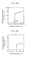
- Fig. 24 is a graph showing a relationship between the specific resistance and temperature of a Y-Ba-Cu-O oxide in
Exmaple 9. - Fig. 25 is a graph showing a relationship between the specific resistance and temperature of a La-Sr-Cu-O oxide in Example 9.
- Fig. 26 is a diagrammatical cross-sectional view of an embodiment of this invention, i.e., a semiconductor device having a multilayer wiring board in Example 9.
- Fig. 27 is a diagrammatical view of a composite having three layers of a superconductive oxide of Example 10.
- Figs. 28(a), 28(b) and 28(c) are pictorial views of an embodiment of this invention, i.e., a superconductive coil of Example 11.
- Figs. 29(a), 29(b), 29(c), 29(d), 29(e) and 29(f) are pictorial views of an embodiment of this invention, i.e., a superconductive magnet of Example 12.
- Figs. 30(a) and 30(b) are pictorial view of an embodiment of this invention, i.e., a non-inductive winding of Example 13.
- Fig. 31 is a diagrammatical view of a permanent current switch using the non-inductive winding of Example 13.
- Figs. 32(a) and 32(b) are diagrammatical views explaining shielding effects of a superconductive shield in Example 15.
- Figs. 33(a) and 33(b) are diagrammatical views of a superconductive power transmission wire improved according to this invention.
- The oxides to be treated according to this invention may include perovskite oxides, layer perovskite oxides, oxygen-deficient layer perovskite oxides, multilayer perovskite oxides, spinel oxides and oxides having similar crystal structures. The spinel type oxides have a structure of AB₂O₄, wherein A is an alkali metal and B is a transition metal, and it is typically LiTi₂O₄, which is schematically shown in Fig. 1, in which A site is occupied by Li and B site occupied by Ti. Fig. 2 schematically shows a structure of the perovskite oxides of ABO₃, wherein A is Ba, Pb, La, Pr or Nd and B is Cu, Mg, Mn, Fe, Co or Ni, or A1-xAʹxBO₃, wherein Aʹ is Ca, Ba, Sr or Pb, such as BaPb1-xBixO₃, BaPbO₃, LaCuO₃, LaCoO₃, (La1-xSrx)CoO₃, (La1-xSrx)CrO₃, (La1-xSrx)CrO3-δ or SrFeO₃. The layer perovskite oxides are represented by A₂BO₄, wherein A is a rare earth metal and B is a transition metal, typically La₂CuO₄, as shown in Fig. 3 in which K, Ni and F correspond to La, Cu and O, respectively, or La₂NiO₄. The oxygen-dificient layer perovskide oxides have a structure of AB₂C₃O7-x, wherein A is Y, La, Nd, Dy, Sm, Eu, Gd, Ho, Tm or Yb, B is Ba, Sr, Ca or Sc and C is mainly Cu, such as YBa₂Cu₃O7-x, LnBa₂Cu₃O7-x wherein Ln is a lanthanoid as indicated above, YSr₂Cu₃O7-x, YBa₂CuO3-xNixO7-y, YBa₂Cu3-xAgxO7-y, YBaCaCu₃O7-x, Y0.75Sc0.25Ba₂Cu₃O7-x or YBa₂Cu₃F₂Oy. A typical example of the oxygen-dificient layer perovskite oxides is YBa₂Cu₃O₇ as shown in Fig. 4. The multilayer perovskite oxides have a structure of A₂(B,C)₃D2+xO₈ or similar compositions wherein A is Bi or Tl, B is Ba or Sr, C is Ca and D is Cu, such as Bi₄Sr₃Ca₃Cu4+xO₁₆ or Tl₄Ba₂Ca₂Cu4+xO₁₆. A typical example of the multilayer perovskite oxides is Bi₄Sr₃Ca₃Cu4+xO₁₆, as shown in Fig. 5.
- In this invention, these superconductive oxides are either converted to non-superconductive oxides, or non-superconductive oxides having compositions capable of being converted to superconductive oxides are converted to the superconductive oxides by applying particle beams or electromagnetic radiations to these superconductive or non-superconductive oxides to increase or reduce the oxygen content of the oxides.
- Furthermore, in this invention, superconductive devices can be made by utilizing the conversion either of from the superconductive oxides to non-superconductive oxides, or from the non-superconductive oxides to superconductive oxides as mentioned above.
- The superconductive devices herein means any of a superconductive magnet, superconductive power transmission wire, superconductive transformer, superconductive shield, permanent current switch and electronic element such as semiconductor chip containing a superconductive circuit or wiring.
- The "particle" of the particle beams used in this invention means ion, electron, neutron and etc. The "electromagnetic radiations" used in this invention mean laser light or infrared rays.
- In order to enrich oxygen at the crystal lattice sites of non-superconductive oxides or superconductive oxides by applying the particle beams or electromagnetic radiations to these oxides so as to obtain a high Tc temperature, the particle is preferably oxygen ion or electron and the electromagnetic radiations are preferably laser light or infrared rays. The application of the radiations is preferably carried out while heating in an oxygen atmosphere.
- In order to remove oxygen at the crystal lattice sites of non-superconductive or superconductive oxides by applying the particle beams or electromagnetic radiations to the oxides, the preferred particles are any ions of elements such as not only hydrogen and oxygen but also titanium, vanadium, chromium, manganese, iron, cobalt, nickel, zinc, silicon, nitrogen, aluminum and magnesium, electrons and neutrons. The particle beams, except for hydrogen beam, should have an energy exceeding that capable of displacing oxygen atoms at the crystal lattice sites of the oxides.
- In order to convert superconductive oxides to non-superconductive oxides, the particle beams may be beams of not only hydrogen and oxygen but also titanium, vanadium, chromium, manganese, iron, cobalt, nickel, zinc, silicon, nitrogen, aluminum and magnesium, electron or neutron. These beams except for hydrogen ions are required to have an energy exceeding that capable of displacing oxygen atoms occupied at the crystal lattice sites. Furthermore, electromagnetic radiations used are preferably laser light or infrared rays. The application of the electromagnetic radiations is preferably carried out in an oxygen-free atmosphere.
- As particles suitable for a particle beam by which fine radiation defects are introduced into superconductive oxides to improve the Jc of the oxides are preferred electrons and ions, particularly electrons, because the application of neutrons gives such drawbacks that oxides are radioactivated or such application requires a long period of time. The electrons and ions do not have such drawbacks. Furthermore, the electrons can control the size or distribution of the radiation defects introduced, with good accuracy. The amount of the electrons applied is preferably in the range of about 60 to 200% of that at which Tconset begins to be reduced.
- Other advantages of the process of this invention for producing superconductive oxides by application of particle beams and of the superconductive oxides will be briefly explained below. Figs. 12 and 13 show the electric resistance-temperature curve and a change of the critical current density Jc in a magnetic field, respectively, of a BiSrCaCu₂Ox thin film made by sputtering, with a 2 MV-electron beam applied at room temperature. This thin film was nearly in a monocrystal form. From Fig. 12 it is clear that the application of electrons tends to afford the reduction of Tc, and from Fig. 13, it is clear that the Jc in a magnetic field increases as the amount of electrons applied increases. The causes for this are considered that fine radiation defects introduced by the application of electrons function as pinning centers. As is seen from the foregoing, superconductive oxides improved in the Jc thereof by the well-controllable application of electrons or ions and superconductive devices using such superconductive oxides as elements fall within the scope of this invention.
- In one aspect of this invention, superconductive devices can be prepared by applying particle beams or electromagnetic radiations to a non-superconductive or superconductive oxide layer at a predetermined region(s), said layer being formed on an insulative substrate, to convert the non-superconductive oxide to superconductive oxide and the superconductive oxide to non-superconductive oxide. In an embodiment of the superconductive devices, a superconductive region such as a circuit may be prepared within the non-superconductive layer by applying a particle beam or electromagnetic radiation to the layer at a predetermined circuit pattern. Similarly, in another embodiment, a beam or radiation-applied non-superconductive region or insulative region may be prepared within a superconductive layer formed on an insulative substrate.
- In the above-mentioned three cases of oxygen-enriching a non-superconductive oxide or superconductive oxide, converting a non-superconductive oxide to a superconductive oxide and preparing the superconductive devices comprising a non-superconductive layer containing a superconductive region therein, the application of particle beams or electromagnetic radiations is preferably carried out while or followed by heat treating the oxides at a temperature between the complete solid solution temperature T of the oxides and T/3 (one-third of T), most preferably between T and 4/5T (four-fifth of T). These temperature ranges are suitable for recovering crystal lattices disordered by application of particle beams or electromagnetic radiations.
- In this invention, there is provided a superconductive oxide having radiation defects introduced by applying particle beams, preferably an ion beam, most preferably an electron beam to the oxide. This superconductive oxide has a high critical current density Jc in a magnetic field. The amount of beam applied is preferably about 60-200% of that at which a critical temperature Tc begins to be lowered by the application.
- For applying ion beams, various ion accelerators may be used. For example, Cockcroft-Walton accelerator, Van de Graaff accelerator, Tandem accelerator, Kaufmann accelerator and etc. may be used. For applying electron beam, Linack accelerator or Cyclotron besides the Cockcroft-Walton accelerator may be used.
- The process for enriching oxygen at the crystal lattice sites of a non-superconductive or superconductive oxide by applying particle beams or electromagnetic radiations to the oxide will be detailedly explained below. For example, the oxygen-deficient layer perovskite oxide exhibits either superconductivity or non-superconductivity depending upon the oxygen content at the crystal lattice sites of the oxide. The present inventors have found that the non-superconductive oxide can be converted to a superconductive oxide and the critical temperature Tc of the superconductive oxide can be raised up by applying oxygen ion beam, or applying electron beam, laser or infrared rays in an oxygen atmosphere. Fig. 7 qualitatively shows an example thereof. Application of oxygen ions at a certain amount to an oxygen-highly deficient trilayer perovskite oxide (non-superconductive area A) allows the oxide to be converted to a superconductive oxide exhibiting a critical temperature. Furthermore, Tc increases as the amount of oxygen ions applied increases. However, further continued application of oxygen ions allows the Tc to reach the maximum l further continued application allows the Tc to decrease as the amount of oxygen ions applied increases, and eventually reach the non-superconductive area C in Fig. 7. The amount of oxygen ions applied at which the Tc reaches the maximum is affected by the applying temperature and applying dose and not linearly determined. The higher the applying temperature and the applying dose, the greater the amount of oxygen ions applied at which the Tc reaches the maximum has a tendency to get. On the other hand, when the amount of oxygen ions applied exceeds a certain value, the Tc begins to decrease, because oxygen atoms at crystal lattice sites are preferentially displaced due to radiation defects by applying oxygen ion beam to reduce the oxygen content at crystal lattice sites. This was confirmed during application of oxygen ions by in-situ observation with a lattice image through a 200 keV electron microscope provided with an ion accelerator. Therefore, it is considered that the peak of the curve in Fig. 7 showing a relationship between a Tc and an amount of oxygen ions applied is produced by concurrence of the reaction in which oxygen atoms applied are introduced into the lattice sites and the reaction in which oxygen atoms are displaced from their lattice sites when applied. Thus, in order to raise up the Tc, oxygen atoms are preferably introduced by applying oxygen beam into the lattice sites until the Tc reaches the peak as shown in Fig. 7.
- On the other hand, as a process for raising up the Tc by converting a non-superconductive oxide within the area A of Fig. 7 to a superconductive oxide, application of electron beam, laser light or infrared rays in an oxygen atmosphere is effective, an example of this process is diagrammatically shown in Fig. 8. The application of electron beam, laser light or infrared rays to oxygen-highly dificient triple layer perovskite oxide (non-superconductive area D) in an oxygen atmosphere allows the oxide to be converted to a superconductive oxide exhibiting a critical temperature when the energy density exceeds a certain value. Furthermore, the Tc increases as the energy density increases. There is a limited range of energy density within which the Tc is permitted to increase. If the energy density is too high, the Tc is rapidly reduced or the oxide is again converted to a non-superconductive oxide (area F in Fig. 8). The mechanism by which non-superconductive oxides are converted by applying electron beam, laser light or infrared rays onto the oxides to superconductive oxides, is considered that the non-superconductive oxides are heated by the application at the applied regions thereof, in which oxygen atoms are introduced (oxidization) from the ambient atmosphere, so that the enrichment of oxygen at the crystal lattice sites are attained. On the other hand, if the energy density of particles applied is too high, the Tc is reduced or the superconductive oxides are again converted to non-superconductive oxides (area F in Fig. 8). This conversion is considered to occur due to the change of structure by the increase of temperature accompanied by evaporatoin of constituent elements of the superconductive oxides, melting of the oxides or amorphization of the oxides. For example, Figs. 9A, 9B and 9C are graphs showing a relationship between the Y/(Y+Ba+Cu), Ba/(Y+Ba+Cu) and Cu/(Y+Ba+Cu) molar ratios, respectively, and the temperature of YBa₂Cu₃O7-x elevated when a laser light applied, and they illustrate that the composition of the oxide are changed by heating. This oxide, YBa₂Cu₃O7-x, is a thin film prepared on an MgO substrate by RF magnetron sputtering. It is clear that the composition of the oxide is remarkably changed when its temperature exceeds 700°C.
- The effect of the radiation defects by which oxygen atoms at crystal lattice sites are displaced, as referred to with Fig. 7, is not only produced by application of oxygen ions but also by application of various other ions, electron or neutron. However, application of hydrogen ions permits the oxygen content at crystal lattice sites of oxides to be reduced through a specific mechanism other than the displacement of oxygen atom. That is, hydrogen ions applied and introduced into oxides cut preferentially bonds of copper atoms and oxygen atoms which are considered to contribute to superconduction, so that the oxygen atoms of the superconductive oxides are reduced with ease. Fig. 10 shows two X-ray diffraction patterns evidencing that reduction of oxygen in an oxide superconductor takes place when a hydrogen ion beam is applied. In Fig. 10, the upper pattern is directed to a non-applied thin film (10 µm in thickness) of YBa₂Cu₃O7-x as prepared by RF magnetron sputtering, whereas the lower pattern concerns the same film to which a hydrogen ion beam of 400 keV was applied at a dose of 10¹⁷H⁺/cm² and at room temperature. It is apparent from Fig. 10 that the non-applied oxide was in a single orthorhombic phase of YBa₂Cu₃O7-x and the applied oxide was transformed into a tetragonal phase of YBa₂Cu₃O7-x and new phases of Y₂BaCuO₅ and CuO were produced. The transformation of YBa₂Cu₃O7-x from the orthorhombic phase to the tetragonal phase takes place when the oxygen content of YBa₂Cu₃O7-x is reduced. So the transformation reveals that the oxygen content is reduced by application of a hydrogen ion beam. This is explained by the following chemical equations:
YBa₂Cu₃O7-x(orthorhombic) + y(2H) → YBa₂Cu₃O7-x-y(tetragonal) + yH₂O (1)
That is, hydrogen atoms introduced by application of a hydrogen ion beam reduces oxygen to induce the transformation from the orthorhombic phase to the tetragonal phase. According to the equation (1) above, H₂O must be formed. The formation of H₂O can be rationally elucidated by the fact that Y₂BaCuO₅ and CuO were newly formed by application of a hydrogen ion beam. In short, the reaction of YBa₂Cu₃O7-x with H₂O can be represented by the following equation:
3H₂O + 2YBa₂Cu₃O6.5 → Y₂BaCuO₅ + 3Ba(OH)₂ + 5CuO (2)
when x is 0.5 for convenience. In this equation, Ba(OH)₂ is not crystallized and hence there appear no peaks of Ba(OH)₂ in the X-ray diffraction patterns of Fig. 10. Thus, the application of a hydrogen ion beam to a superconductive oxide allows oxygen atoms at crystal lattice sites to be reduced with ease. Fig. 11 is an electric resistance-temperature curve evidencing that the thin film of a superconductive oxide, YBa₂Cu₃O7-x, referred to in Fig. 10 can be converted to a non-superconductive oxide. - As is clear from the foregoing, one aspect of this invention is to provide a process for forming a non-superconductive oxide region in a superconductive oxide layer falling within superconductive area B or E of Fig. 7 or 8 by the method for reducing the oxygen content of the superconductive oxide, as explained above and further to provide a superconductive device such as a superconductive circuit or wiring by forming non-superconductive regions of a predetermined pattern in a superconductive oxide layer through the above-mentioned process. Furthermore, another aspect of this invention is to provide a semiconductor device comprising semiconductor elements having the superconductive circuit or wiring formed thereon by the above-mentioned process.
- Figs. 12 and 13 show an electric resistance-temperature curve and a change of critical current density in a magnetic field, respectively, of a thin film (5 µm thick) of BiSrCaCu₂Ox prepared by sputtering in applying an electron beam of 2 MV to the thin film at room temperature. The thin film is nearly in a monocrystal form. It is seen from Fig. 12 that Tc tends to decrease as the amount of the electron beam applied increases, whereas it is seen from Fig. 13 that Jc tends to increase as the amount of the electron beam applied increases. Thus, it is also within the scope of this invention to raise up the critical current density Jc of a superconductive oxide by applying an ion beam, electron beam or neutron beam to the oxide.
- The invention will be illustrated with reference to some exmaples below.
- This example is one of embodiments of a process for controlling the oxygen content at the crystal lattice sites of non-superconductive oxides or superconductive oxides by applying oxygen ions to the oxides. Table 1 shows samples and a method for preparing the samples. Sixty (60) samples in total of six kinds of compositions wherein x is 0.05, 0.1, 0.2, 0.3, 0.4 and 0.5, were prepared as shown in Table 1. These samples were injected by oxygen ions to 1 × 10¹⁷ ions/cm² with a Cockcroft-Walton ion accelerator. This ion accelerator was operated under the following conditions: an accelerating voltage of 0.4 MeV, a degree of vacuum of 10⁻⁶ to 10⁻⁷ Torr in a sample chamber or vacuum chamber and a temperature of 870 to 1100 K. Fig. 14 is a pictorial view of the appearance of the ion accelerator. Fig. 15 is a diagram illustrating the structure of the ion accelerator as shown in Fig. 14, and the path of an ion beam. Oxygen to be injected is supplied from
oxygen bottle 5 toion source 6, to which high voltage is applied to form oxygen ions. An ion beam is injected into sample 11 invacuum chamber 3 through quaternarypolar lens 2,polarizer 9 and slit 10 from accelerator 1 constituted byion source 6,mass spectrometer 7 and acceleratingtube 8. A carbonic acid gas bottle may be used in place of the oxygen bottle to generate oxygen ions. Furthermore,electromagnet 12,ammeter 13 for the accelerating tube,power source 14 for the quaternary polar lens,ammeter 15 for the polarizer,ammeter 16 for the slit,ammeter 17 for target and temperature-measuring and regulatingelement 18 are connected tomicrocomputer 19 and regulated by the microcomputer so as to maintain the injection conditions to be constant. The oxygen ion-injection was carried out on the thin film samples at both the sides thereof under the same conditions, except for Groups C and D. - The samples injected by oxygen ions were cooled to the temperature of liquid helium. During the cooling, a change of inductance was measured by an inductance method, to examine the critical temperature Tc. Fig. 16 is a graph showing an example of the measurements for the samples (for Sample No. 1 shown in Table 1, wherein x is 0.1). In Fig. 16, the abscissa indicates absolute temperature and the ordinate inductance. In the example, it is clear that Tc is 35 K.
- Table 2 shows an increase or decrease of the critical temperature Tc of the sampels treated above compared with that of a non-injected sample measured in the same manner. The sample having a decreased Tc was recovered or improved by annealing after the ion-injection.
- Table 3 shows a proportion of a difference in an increase of temperature between the maximum Tcmax of the sample ion injected by the accelerator and the critical temperature Tc⁰ of a non-injected sample to Tc⁰: (Tcmax - Tc⁰)/Tc⁰. The proportion varies depending upon the values of x of the samples but it is clear that all the samples had a Tc increased by the process of this invention. The superconductive oxides, as shown in Table 3, having a higher Tc than the Tc⁰, obtained by controlling the oxygen content of the oxides according to the process of this invention fall within the scope of this invention.
- The application of oxygen ions was carried out in the same manner as in EXAMPLE 1. Samples were thin films (1 - 2 µm thick) of YBa₂Cu₃O6.2, YBa₂Cu₃O6.6 and ErBa₂Cu₃O6.5 prepared on MgO substrates by the RF magnetron sputtering. This application of oxygen ions were carried out with a Cockcroft-Walton ion accelerator (Figs. 14 and 15) at 75 keV and 1110 ±30 K. Fig. 17 shows a change of the Tcoffset of the samples with respect to the amount of oxygen ions applied. Before the application of oxygen ions, YBa₂Cu₃O6.2 was a non-superconductor, YBa₂Cu₃O6.6 was a superconductor having a Tcoffset of 54 K, and ErBa₂Cu₃O6.5 was a superconductor having a Tcoffset of 51 K. The application of oxygen ions allowed the non-superconductor to be converted to a superconductor, and the Tc of the superconductors was raised up until the amount of oxygen ions applied reached a certain level, as shown in Fig. 17. Further increase in the amount of oxygen ions applied begins to allow the oxygen atoms at the crystal lattice sites to be displaced, so that the Tc was reduced. The application of 10¹⁹ O⁺/cm² allowed all the samples to be converted to non-superconductors.
- Pellet samples of a non-superconductive YBa₂Cu₃O6.2 with 25 mm in length, 6 mm in width and 3 mm in thickness were prepared by the oxide-mixing method. Fig. 18 is a graph showing a change of the critical temperature of the samples, as carbonic acid gas laser or electron beam is applied to the samples, with respect to the energy density applied. The electron beam was applied at a range of 50 to 100 keV. In both the cases of applying the electron beam and the carbonic acid gas laser, the similar results were obtained. The transformation from the non-superconductive form to the superconductive form began to occur at an energy density of about 1 × 10² J/cm². The critical temperature increased as the energy density increased, but it began to decrease when the energy density exceeded about 2 × 10³ J/cm², and the samples began to be molten at about 4.3 × 10³ J/cm² to be again transformed to the non-superconductive form.
- A thin film sample (5 µm in thickness) of YBa₂Cu₃O7-x was prepared on a substrate of MgO by RF megnetron sputtering. Fig. 19 is a graph showing an influence of an amount of hydrogen ions applied on a electric resistance-temperature curve of the sample when a 400 keV hydrogen ion beam was applied. The application was carried out at room temperature with a Cockcroft-Walton accelerator. The Tcoffset of the sample began to decrease when the amount of hydrogen ions applied exceeded the order to 10¹⁵ H⁺/cm². The sample was converted to a non-superconductive oxide at an applied amount of an order of 10¹⁷ H⁺/cm².
-
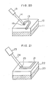
Semiinsulative layer 12 having a composition of YBa₂Cu₃O6.0 and a thickness of about 200 nm was formed by sputtering on substrate 11 of an Si single crystal having a crystal direction of (100). The resultant sample was heated to 1000°C for about 1 hour under vacuum and then cooled. Selected part of thesemiinsulative layer 12 was heated to a temperature of 800 to 500°C (at least 500°C) with laser light 14 fromCO₂ laser 15 or an infrared ray in pure oxygen of 1 atm. At the heated part the composition was converted to YBa₂Cu₃O₇ (superconductor 13). The contour of thesuperconductor 13 could optionally be made by movingbeam spot 16. (The contour can also be made by moving the substrate 11 or sweeping the laser light with an optical means.) According to this example, a semiinsulative substrate was automatically made of thesemiinsulative layer 12, so that thesuperconductor 13 was embedded into the semiinsulative substrate orsemiinsulative layer 12. The top surfaces of thesemiinsulative layer 12 and thesuperconductor 13 were in the same plane or had no step formed therebetween. Therefore, high integration of circuits using thesuperconductor 13 is advantageously possible. The minimum size of thesuperconductor 13 is predominantly determined by the diameter of thebeam spot 16 or thelaser light 14. The diameter may be as small as 1 µm. - In this example, the locallized oxidation of the
semiinsulative layer 12 was carried out by heating with a laser light in oxygen as mentioned above, but this heating with a laser light may be replaced with high-frequency heating to a temperature of 800 to 500°C. The oxygen pressure is not limited to 1 atm. To oxide the locallized parts effectively, it is desirably higher than 1 atm at a temperature of 800 to 500°C. Further, a cooling rate after the heating may vary depending upon the sweeping rate of the spot of laser light. However, for the purpose of obtaining a small amount of crystal faults, the sweeping rate is as low as possible and the coolihg rate is desirably maintained at about 5 deg/minute down to about 500°C. - In the example as shown in Fig. 20, the
superconductor 13 may be used as wiring of circuits. - Contrary to the EXAMPLE 5 in which the
semiinsulative layer 12 was preformed,superconductive layer 22 was preformed onsubstrate 20. Thissuperconductive layer 22 was applied byhydrogen ion beam 24 fromhydrogen ion source 23. Thesuperconductive layer 22 may be reduced and converted tosemiinsulative layer 21 at thebeam spot 25. In this example, thesuperconductive layer 22 constituted a wiring. In applyinghydrogen ion beam 24, thesubstrate 20 is desirably heated to about 500°C but this heating is not always necessary. In this example, hydrogen ion beam was used for converting thesuperconductive layer 22 to thesemiinsulative layer 21 but instead other reducing ion beams may be used. Further, heating under vacuum to 800°C or higher by laser light or high-frequency allows oxygen to be dissociated in theregion 21 and, therefore, such heating is also effective for achieving the object of this invention. - In this example, a tunnel element using the superconductive oxide was prepared according to this invention.
Semiconductive layer 32 of YBa₂Cu₃O5.0 having a thickness of about 200 nm were formed by sputtering on a silicon or saphire substrate. This layer on the substrate was subjected to the heat treatment in oxygen in the same manner and under the same conditions as in EXAMPLE 1. Thus, thesuperconductor 33 was formed as shown in Fig. 22(a). The width of thesuperconductor 33 was about 20 µm in this example but in general it is not particularly limited. Therefore,tunnel region 31 was formed by injecting hydrogen ions under the same conditions as in EXAMPLE 2, as shown in Fig. 22(b). The ion beam was converged so that the width of this region was about 10 to 50 nm. Thetunnel region 31 may be converted to semiinsulator or conductor by changing an amount of ions injected. In both the cases it is apparent that it can be used as a superconductive weak-link. Thus, it is clear that a superconductive weak-link device having a flat structure can be prepared without using any photolithography or etching technique, according to the process of this invention. - This example will be described with reference to Fig. 23.
-
Semiinsulative layer 43 having a composition of YBa₂Cu₃O5.0 was formed onsubstrate 44 of saphire in the same manner as in EXAMPLE 5 and then subjected to the local heat treatment in an oxygen atmosphere at a temperature of 800 to 500°C in the same manner as in EXAMPLE 5 to form a first layer ofsuperconductive wiring 41. Subsequently, asemiinsulative layer 40 having a composition of YBa₂Cu₃O5.0 was formed on the first layer, and then subjected to local oxidation with a laser beam to form a second layer ofsuperconductive wiring 42. Thus, it is clear that double-layer superconductive wiring can easily be realized according to the process of this invention. As is seen in Fig. 23, each layer was flat and hence multilayer wirings can also easily be realized to improve the performance of circuits. - These superconductive wirings can be used together with a semiconductor device such as a MOS transistor. In this example the oxide material was used as the superconductive or semiinsulative material having a composition of YBa₂Cu₃O7-δ, but Y may be replaced with Gd, Lu, Eu, Sc, Co, Sm, Nd, Yb, Tb or Ho and Ba with Sr or Ca to obtain the same effect.
- Samples were a Y-Ba-Cu-O oxide prepared by RF magnetron sputtering (target materials: Ba₂CuO₃ and Y₂O₃; substrate material; saphire, SrTiO₃ and quartz; and substrate temperature: 700°C or lower) and a monocrystalline La-Sr-Cu-O oxide prepared by molecular beam epitaxy. Both the samples had a thickness of about 0.5 to 1 µm.
- Figs. 24 and 25 are graphs showing a relationship between the specific resistance and the temperature of the samples, Y-Ba-Cu-O and La-Sr-Cu-O oxides, respectively.
- Table 4 shows how to convert to non-superconductive oxides according to the process of this invention, whether or not the conversion to non-superconductive oxides occurred and wheter or not the conversion to insulative oxides occurred. Even oxides not converted to insulative oxides exhibited a specific resistance of several figures higher than that as shown in Fig. 25 by choosing ion species and controlling the amount of ions doped. The ion doping was carried out by a Cockcroft-Walton accelerator or tandem type accelerator. These accelerators were properly used depending upon an accelerating voltage applied.
- Fig. 26 is a cross-sectional view of an example of semiconductive devices having the superconductive wiring boards prepared according to the process of this invention. That is,
superconductive oxide 55 was formed by sputtering oninsulative film 53 provided on semiconductive element 56 (at thisstage regions 54 were the same material as the oxide 55). Thereafter, regions to become wirings were masked and selectively ion-doped to forminsulative regions 54. This process was repeated to make a multilayer wiring board as shown in Fig. 26.Insulative regions Resistance 50 was also made by the ion-doping step. - Conductive or
insulative layer 61 was formed by ion doping onsuperconductive oxide layer 60 prepared by sputtering, vacuum evaporation or chemical vaporization. This step was repeated to form a composite comprising a three-layer structure which has twolayers 61 interposed therebetween. Fig. 27 is a cross-sectional view of the composite. Thus, a composite having a structure of two or more layers of superconductive oxides and similar oxides integrated. - This example is directed to the preparation of a superconductive magnet element and will be described with reference to Fig. 28. Y₂O₃, BaCO₃ and CuO were weighed and mixed at a Y:Ba:Cu atomic ratio of 1:2:3, calcined at 900°C for 24 hours and pulverized. The calcined powder was kneaded with pineoil and an organic binder to form a paste, which was then coated on the peripheral surface of
cylindrical tube 72 of a non-superconductor such as Zr and heat treated at 950°C for 1 hour to formsuperconductive layer 71, as shown in Fig. 28(a). The cylindrical tube coated with the superconductive layer as shown in Fig. 28(a) was rotated in a direction indicated byarrow 76 and at the same time moved in a direction indicated byarrow 73, whileparticle beam 75 was applied to thesuperconductive layer 71 at selected regions, as shown in Fig. 28(b). As particles of theparticle beam 75 may be used whatever is capable of giving radiation defects to thesuperconductive layer 71, for example, ions or electrons. Theparticle beam 75 may be replaced with electromagnetic radiation such as laser and etc., particularly which is preferably a ray having an energy density in an order of 103 J/cm². The region of thelayer 74 on which thebeam 75 was applied was converted to non-superconductive oxide in the same mechanism as in any of EXAMPLES 2 to 6 and 8 to 10. In this example, thenon-superconductive region 74 was made in a spiral form as shown in Fig. 28(c), right-hand diagram. The non-applied region was asuperconductive coil 77. One or moresuperconductive coils 78 having a size different from that of thesuperconductive coil 77 were made in the same manner as mentioned above, as shown in Fig. 28(c), left-hand diagram. The superconductive magnet element was made by coaxially inserting thecoil 77 into thecoil 78, as shown in Fig. 28(c). Thesuperconductive layer 71 on the cylindrical tube as shown in Fig. 28(a) may not only be made by coating as mentioned above, but also by other ways such as solidification of a molten state. Furthermore, the outer surface of the non-superconductor 72, which has compositions capable of being converted to superconductive oxides, may be converted to a superconductor in the same manner as in EXAMPLES 1 to 3 to form the coil. - A superconductive magnet as shown in Fig. 29 was made by the process of this invention.
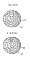
Disks 190 of a superconductive oxide, which had a hole at the center thereof as shown in Fig. 29(a) were prepared. The same particle beam or electromagnetic radiation as in any of EXAMPLES 2 to 6 and 8 to 11 was applied onto these disks at thescroll part 81 thereof as shown in Fig. 29(b). This application to thescroll part 81 was carried out by maskingscroll part 82 for some disks or converging and sweeping the beam or radiation onto thepart 81 for the other disks. Thus, thepart 81 was selectively converted by this application to a non-superconductive oxide and the remainingpart 82 formedsuperconductive coil 191. Furthermore,superconductive coil 192 having a counterrotating scroll part as shown in Fig. 29(c) was made in the same manner as mentioned above. In Figs. 29(b) and 29(c), this scroll part was formed in the direction of thickness at any cross-sections of the disks. Then, as shown in Fig. 29(d), the superconductive coil of Fig. 29(b) was converted to a non-superconductive oxide only on the surface thereof, except for theend 83 at the periphery of thepart 82, and then also at the backside surface, except for theend 84 at the periphery of the central hole, in the same manner as mentioned above. Then, as shown in Fig. 29(e), the superconductive coil of Fig. 29(c) was also converted to a non-superconductive oxide only on both the front and backside surfaces thereof, except for the peripheral ends 84 and 83 of the respective surfaces, in the same manner as mentioned above. Thus, coils 193 of Fig. 29(d) and 194 of Fig. 29(e) were obtained. Then, thecoils coil 193 and the front surface ofcoil 194 on each other so that theend 84 ofcoil 193 and theend 84 ofcoil 194 were connected to each other. Some of the units were stacked so that theend 83 of one unit and theend 83 of another unit were connected to each other to form a long superconductive coil. The coupling was carried out by heat treatment under such conditions that the non-superconductive oxide was not converted to the superconductive oxide. - In this example, a non-inductive coil was made by the process of this invention. Fig. 30(a) shows the same coil as the
coil 193 as shown in Fig. 29(d) for EXAMPLE 12. Fig. 30(b) showscoil 195 which was made by converting the superconductive oxide of the same coil ascoil 191 of Fig. 29(b) only on both the front and backside surfaces thereof, except for theend 85 on the front surface at the inside periphery and theend 86 on the backside surface at the outside periphery. Thus,coil 195 was obtained. Theend 84 ofcoil 193 was connected to theend 85 ofcoil 195 and then theend 86 ofcoil 195 to theend 83 ofcoil 193 by the same heat treatment as that of EXAMPLE 12. This connection was repeated to form the non-inductive superconductive coil. This non-inductive coil was used as asuperconductive coil 211 of permanent current switch as shown in Fig. 31. On switching off at 212, electric resistance of 211 becomes higher. Therefore, the permanent current switch having a high performance was made. 213 denotes a direct current power source. - The size of the long coil as shown in Fig. 29(f) or the stacked number of
coils - Figs. 32(a) and 32(b) show an example of superconductive shields having an shielding effect improved by the process of this invention. In Fig. 32(a), 221 denotes a magnetic shielding device made of a superconductive oxide, YBa₂Cu₃O7-x. To this
device 221 was applied an electron beam of 2 MeV at 250 K and 7 × 10¹⁷ e/cm², thus obtaining a shielding device having radiation defects 223 introduced therein, as shown in Fig. 32(b). The Jc of thedevice 221 was raised from 800 A/cm² to about 1440 A/cm² (about 1.8 times). When a magnetic field was applied to the device, it was found that the shielding effect was improved. - Figs. 33(a) and 33(b) show an example of superconductive power transmission wires having a performance improved by the process of this invention. In Fig. 33(a), 231 denotes a power transmission wire comprising a superconductive oxide of (La0.9Sr0.1)₂CuO₃. To this wire was applied an electron beam of 2 MeV at 250 K and 5 × 10¹⁷ e/cm², thus obtaining a power transmission wire having
radiation defects 233 introduced therein, as shown in Fig. 33(b). The Jc of the wire as shown in Fig. 33(a) was 280 A/cm², wehreas the Jc of the wire as shown in Fig. 33(b) was about 1.5 times greater than that of the wire as shown in Fig. 33(a). Thus, it was found that the wire was improved by the treatment according to this invention. Liquid He as a cooling medium was indicated by 234.


Claims (20)
Applications Claiming Priority (8)
| Application Number | Priority Date | Filing Date | Title |
|---|---|---|---|
| JP8477087 | 1987-04-08 | ||
| JP84770/87 | 1987-04-08 | ||
| JP90762/87 | 1987-04-15 | ||
| JP9076287 | 1987-04-15 | ||
| JP93025/87 | 1987-04-17 | ||
| JP9302587 | 1987-04-17 | ||
| JP10428387 | 1987-04-30 | ||
| JP104283/87 | 1987-04-30 |
Publications (3)
| Publication Number | Publication Date |
|---|---|
| EP0286106A2 true EP0286106A2 (en) | 1988-10-12 |
| EP0286106A3 EP0286106A3 (en) | 1990-03-28 |
| EP0286106B1 EP0286106B1 (en) | 1995-08-02 |
Family
ID=27467007
Family Applications (1)
| Application Number | Title | Priority Date | Filing Date |
|---|---|---|---|
| EP88105573A Expired - Lifetime EP0286106B1 (en) | 1987-04-08 | 1988-04-07 | Process for manufacturing a superconductive device |
Country Status (5)
| Country | Link |
|---|---|
| US (1) | US5096882A (en) |
| EP (1) | EP0286106B1 (en) |
| JP (1) | JP2876211B2 (en) |
| KR (1) | KR880013187A (en) |
| DE (1) | DE3854238T2 (en) |
Cited By (15)
| Publication number | Priority date | Publication date | Assignee | Title |
|---|---|---|---|---|
| EP0282360A2 (en) * | 1987-03-12 | 1988-09-14 | Semiconductor Energy Laboratory Co., Ltd. | Method for manufacturing components of superconducting ceramic oxide materials |
| EP0285106A2 (en) * | 1987-03-30 | 1988-10-05 | Sumitomo Electric Industries Limited | Method of forming superconducting circuit |
| EP0290271A2 (en) * | 1987-05-08 | 1988-11-09 | Fujitsu Limited | Superconducting circuit board and process of manufacturing it |
| EP0292387A2 (en) * | 1987-05-18 | 1988-11-23 | Sumitomo Electric Industries Limited | Method for producing a superconducting circuit |
| EP0299163A2 (en) * | 1987-07-15 | 1989-01-18 | Sharp Kabushiki Kaisha | Interconnection method for semiconductor device |
| EP0304807A2 (en) * | 1987-08-22 | 1989-03-01 | Sumitomo Electric Industries Limited | Method for producing superconducting circuit |
| EP0311331A2 (en) * | 1987-10-07 | 1989-04-12 | United Kingdom Atomic Energy Authority | Superconducting ceramic circuit elements |
| FR2647266A1 (en) * | 1989-05-17 | 1990-11-23 | Ecole Cle Arts Manufactures | Electrical or electronic circuit element including a super-conductor to which conducting elements are fixed |
| FR2670201A1 (en) * | 1990-12-06 | 1992-06-12 | Dornier Gmbh | PROCESS FOR MICROSTRUCTURING SUPERCONDUCTING OXIDE CERAMICS. |
| US5143894A (en) * | 1987-10-14 | 1992-09-01 | Mordechai Rothschild | Formation and high resolution patterning of superconductors |
| US5194419A (en) * | 1989-07-25 | 1993-03-16 | The Furukawa Electric Co., Ltd. | Method for manufacturing an oxide superconductive multilayer circuit |
| WO1998024098A1 (en) * | 1996-11-27 | 1998-06-04 | British Nuclear Fuels Plc | Improvements in and relating to coils |
| EP1070327A1 (en) * | 1998-03-18 | 2001-01-24 | Metal Manufactures Limited | Integrated tape |
| WO2002027765A2 (en) | 2000-09-26 | 2002-04-04 | MAX-PLANCK-Gesellschaft zur Förderung der Wissenschaften e.V. | Stoichiometric modification of an ionic structured solid |
| US8061016B2 (en) | 2001-08-24 | 2011-11-22 | 3-Cs Ltd | Superconducting coil fabrication |
Families Citing this family (58)
| Publication number | Priority date | Publication date | Assignee | Title |
|---|---|---|---|---|
| JPH01111702A (en) * | 1987-10-24 | 1989-04-28 | Hiroyuki Yoshida | Production of room temperature superconductor from composite oxide utilizing irradiation |
| JP2965641B2 (en) * | 1989-08-21 | 1999-10-18 | 松下電器産業株式会社 | Superconducting element manufacturing method |
| JP2767298B2 (en) * | 1989-09-05 | 1998-06-18 | 財団法人生産開発科学研究所 | LAMINATED THIN FILM AND PROCESS FOR PRODUCING THE SAME |
| JPH03151231A (en) * | 1989-10-13 | 1991-06-27 | Internatl Business Mach Corp <Ibm> | Multilayer strain lattice copper oxide perovskite structure |
| EP0478466B1 (en) * | 1990-09-27 | 1995-11-08 | Sumitomo Electric Industries, Ltd. | A superconducting device and a method for manufacturing the same |
| DE69127418T2 (en) * | 1990-09-27 | 1998-03-12 | Sumitomo Electric Industries | Manufacturing process of a superconducting component with an extremely thin superconducting channel made of superconducting oxide material |
| CA2054470C (en) * | 1990-10-30 | 1997-07-01 | Takao Nakamura | Method for manufacturing superconducting device having a reduced thickness of oxide superconducting layer and superconducting device manufactured thereby |
| EP0671764A2 (en) * | 1990-10-31 | 1995-09-13 | Sumitomo Electric Industries, Ltd. | A process for fabricating a superconducting circuit |
| CA2054795C (en) * | 1990-11-01 | 1996-08-06 | Hiroshi Inada | Superconducting device having an extremely thin superconducting channel formed of oxide superconductor material and method for manufacturing the same |
| US5856275A (en) * | 1990-11-01 | 1999-01-05 | Sumitomo Electric Industries, Ltd. | Superconducting wiring lines and process for fabricating the same |
| US6308399B1 (en) * | 1991-06-18 | 2001-10-30 | Dawei Zhou | High-TC superconducting ceramic oxide products and macroscopic and microscopic methods of making the same |
| US5420101A (en) * | 1991-06-24 | 1995-05-30 | Forschungszentrum Julich Gmbh | Structures super conductor tracks and process for making them |
| JP3287028B2 (en) * | 1991-10-25 | 2002-05-27 | 日立電線株式会社 | Tl, Pb-based oxide superconducting material and method for producing the same |
| US5747427A (en) * | 1991-11-15 | 1998-05-05 | Hokkaido Electric Power Co., Inc. | Process for forming a semiconductive thin film containing a junction |
| WO1994002862A1 (en) * | 1992-07-20 | 1994-02-03 | Superconductor Technologies, Inc. | Superconductor thin film crossovers and method |
| JPH06219736A (en) * | 1993-01-27 | 1994-08-09 | Hitachi Ltd | Superconductor |
| WO1995002709A2 (en) * | 1993-07-15 | 1995-01-26 | President And Fellows Of Harvard College | EXTENDED NITRIDE MATERIAL COMPRISING β-C3N¿4? |
| FR2714205A1 (en) * | 1993-12-17 | 1995-06-23 | Atg Sa | Composite material for magneto-optical recording, its preparation and its use. |
| JPH07263767A (en) | 1994-01-14 | 1995-10-13 | Trw Inc | Planer type high-temperature superconducting integrated circuit using ion implantation |
| US5593918A (en) * | 1994-04-22 | 1997-01-14 | Lsi Logic Corporation | Techniques for forming superconductive lines |
| US6153561A (en) | 1996-09-13 | 2000-11-28 | The Ohio State University | Method for oxygenating oxide superconductive materials |
| US6004508A (en) * | 1997-08-01 | 1999-12-21 | The Coca-Cola Company | Method and apparatus for super critical treatment of liquids |
| US6143366A (en) * | 1998-12-24 | 2000-11-07 | Lu; Chung Hsin | High-pressure process for crystallization of ceramic films at low temperatures |
| US6188919B1 (en) | 1999-05-19 | 2001-02-13 | Trw Inc. | Using ion implantation to create normal layers in superconducting-normal-superconducting Josephson junctions |
| US6638895B1 (en) * | 1999-10-27 | 2003-10-28 | The University Of Chicago | Method for fabricating high aspect ratio structures in perovskite material |
| JP4859165B2 (en) * | 2004-06-07 | 2012-01-25 | 独立行政法人物質・材料研究機構 | Superconducting material having high critical current characteristics and manufacturing method thereof |
| WO2006013819A1 (en) * | 2004-08-02 | 2006-02-09 | Matsushita Electric Industrial Co., Ltd. | Resistance change element and resistance change type memory using the same |
| JP4431891B2 (en) * | 2004-12-28 | 2010-03-17 | セイコーエプソン株式会社 | Piezoelectric element, piezoelectric actuator, piezoelectric pump, ink jet recording head, ink jet printer, surface acoustic wave element, thin film piezoelectric resonator, frequency filter, oscillator, electronic circuit, and electronic equipment |
| US7888290B2 (en) * | 2005-09-12 | 2011-02-15 | Armen Gulian | Material exhibiting superconductivity characteristics and method of manufacture thereof |
| JP4984466B2 (en) * | 2005-09-21 | 2012-07-25 | 住友電気工業株式会社 | Superconducting tape wire manufacturing method |
| JP2007224747A (en) * | 2006-02-21 | 2007-09-06 | Mitsubishi Motors Corp | Exhaust emission control filter and exhaust emission control device of diesel engine |
| CN100440388C (en) * | 2006-09-01 | 2008-12-03 | 天津理工大学 | Producing ABO3 type perrovskite structure double oxide ion conductor by laser fusion synthetic method |
| US7615385B2 (en) | 2006-09-20 | 2009-11-10 | Hypres, Inc | Double-masking technique for increasing fabrication yield in superconducting electronics |
| US20080146449A1 (en) * | 2006-12-14 | 2008-06-19 | Jerome Lesueur | Electrical device and method of manufacturing same |
| US8741158B2 (en) | 2010-10-08 | 2014-06-03 | Ut-Battelle, Llc | Superhydrophobic transparent glass (STG) thin film articles |
| FI126113B (en) * | 2009-06-24 | 2016-06-30 | Johannes Frantti | High temperature superconductors |
| WO2011017454A1 (en) * | 2009-08-04 | 2011-02-10 | Ut-Battelle, Llc | Critical current density enhancement via incorporation of nanoscale ba2(y,re) tao6 in rebco films |
| WO2011017439A1 (en) * | 2009-08-04 | 2011-02-10 | Ut-Battelle, Llc | Critical current density enhancement via incorporation of nanoscale ba2renbo6 in rebco films |
| US9435035B2 (en) | 2010-01-15 | 2016-09-06 | Byd Company Limited | Metalized plastic articles and methods thereof |
| CN102071424B (en) * | 2010-02-26 | 2012-05-09 | 比亚迪股份有限公司 | Plastic product and preparation method thereof |
| US8685549B2 (en) | 2010-08-04 | 2014-04-01 | Ut-Battelle, Llc | Nanocomposites for ultra high density information storage, devices including the same, and methods of making the same |
| CN102071411B (en) | 2010-08-19 | 2012-05-30 | 比亚迪股份有限公司 | Plastic product and preparation method thereof |
| US11292919B2 (en) | 2010-10-08 | 2022-04-05 | Ut-Battelle, Llc | Anti-fingerprint coatings |
| US9221076B2 (en) | 2010-11-02 | 2015-12-29 | Ut-Battelle, Llc | Composition for forming an optically transparent, superhydrophobic coating |
| US8748350B2 (en) | 2011-04-15 | 2014-06-10 | Ut-Battelle | Chemical solution seed layer for rabits tapes |
| US8748349B2 (en) | 2011-04-15 | 2014-06-10 | Ut-Battelle, Llc | Buffer layers for REBCO films for use in superconducting devices |
| EP2864239B1 (en) | 2012-06-21 | 2017-12-20 | Monash University | Conductive portions in insulating materials |
| CN103317240B (en) * | 2013-07-12 | 2015-09-30 | 东明兴业科技股份有限公司 | The laser-induced thermal etching processing method of Mg alloy surface oxide layer |
| US9768370B2 (en) * | 2013-09-17 | 2017-09-19 | Varian Semiconductor Equipment Associates, Inc. | Low AC loss high temperature superconductor tape |
| US9590161B2 (en) * | 2013-11-27 | 2017-03-07 | Varian Semiconductor Equipment Associates, Inc. | Laser processing of superconductor layers |
| US20150239773A1 (en) | 2014-02-21 | 2015-08-27 | Ut-Battelle, Llc | Transparent omniphobic thin film articles |
| US9543496B2 (en) * | 2014-03-17 | 2017-01-10 | Uchicago Argonne, Llc | Creation of high-pinning microstructures in post production YBCO coated conductors |
| US10290797B1 (en) * | 2016-02-29 | 2019-05-14 | The United States Of America As Represented By The Secretary Of The Navy | Method for producing high-temperature superconducting films having sharp charge doping discontinuities |
| KR102145354B1 (en) * | 2018-05-31 | 2020-08-18 | 경기대학교 산학협력단 | Method for hydrogen generation having redox cycle by proton beam irradiation and Apparatus for generating hydrogen having the same |
| KR102149059B1 (en) * | 2018-06-01 | 2020-08-28 | 경기대학교 산학협력단 | Method for hydrogen generation having redox cycle by Xenon light or Microwave irradiation and Apparatus for generating hydrogen having the same |
| US11783953B2 (en) * | 2018-10-02 | 2023-10-10 | Massachusetts Institute Of Technology | Cryogenic radiation enhancement of superconductors |
| CN111825444B (en) * | 2020-08-04 | 2022-08-19 | 上海上创超导科技有限公司 | Method for introducing columnar defects into ex-situ high-temperature superconducting thin film |
| CN113470883B (en) * | 2021-06-29 | 2022-11-11 | 南京大学 | Non-toxic copper oxide superconductor with high critical parameter and its preparing process |
Citations (5)
| Publication number | Priority date | Publication date | Assignee | Title |
|---|---|---|---|---|
| EP0008866A1 (en) * | 1978-08-11 | 1980-03-19 | LUCAS INDUSTRIES public limited company | Electrical switches |
| JPS5629383A (en) * | 1979-08-17 | 1981-03-24 | Nippon Telegr & Teleph Corp <Ntt> | Manufacture of tunnel-junction type josephson element |
| EP0282360A2 (en) * | 1987-03-12 | 1988-09-14 | Semiconductor Energy Laboratory Co., Ltd. | Method for manufacturing components of superconducting ceramic oxide materials |
| EP0285030A2 (en) * | 1987-03-27 | 1988-10-05 | Nissin Electric Company, Limited | Process for producing superconducting thin films |
| EP0285106A2 (en) * | 1987-03-30 | 1988-10-05 | Sumitomo Electric Industries Limited | Method of forming superconducting circuit |
Family Cites Families (20)
| Publication number | Priority date | Publication date | Assignee | Title |
|---|---|---|---|---|
| CA631707A (en) * | 1961-11-28 | L. Ruskin Simon | Activated oxide complexes | |
| BE526937A (en) * | 1953-03-05 | 1954-09-03 | ||
| JPS5845194B2 (en) * | 1980-07-11 | 1983-10-07 | 日本電信電話株式会社 | Superconducting integrated circuit and its manufacturing method |
| JPS60173885A (en) * | 1984-02-18 | 1985-09-07 | Nippon Telegr & Teleph Corp <Ntt> | Superconductive material of oxide and manufacture thereof |
| JPS61138417A (en) * | 1984-12-11 | 1986-06-25 | 科学技術庁金属材料技術研究所長 | Manufacture of a-15 type super conducting compound |
| JPS61168530A (en) * | 1985-01-21 | 1986-07-30 | Nippon Telegr & Teleph Corp <Ntt> | Superconductive oxide material and production thereof |
| JPS61206279A (en) * | 1985-03-11 | 1986-09-12 | Hitachi Ltd | Superconductive element |
| JPS62104283A (en) * | 1985-10-31 | 1987-05-14 | Kokusai Denshin Denwa Co Ltd <Kdd> | Noise reduction system for differential decoding signal in animation picture transmission |
| JP2610613B2 (en) * | 1986-07-22 | 1997-05-14 | 日産自動車株式会社 | Photochromic materials for automobiles or building materials |
| JP2660281B2 (en) * | 1987-02-24 | 1997-10-08 | 株式会社 半導体エネルギー研究所 | Superconductor fabrication method |
| JP2660280B2 (en) * | 1987-02-24 | 1997-10-08 | 株式会社 半導体エネルギー研究所 | Superconductor |
| JPS63224116A (en) * | 1987-03-11 | 1988-09-19 | Matsushita Electric Ind Co Ltd | Manufacture of thin film superconductor |
| JP2645489B2 (en) * | 1987-03-12 | 1997-08-25 | 株式会社 半導体エネルギー研究所 | Superconductor fabrication method |
| JPS63250881A (en) * | 1987-04-07 | 1988-10-18 | Semiconductor Energy Lab Co Ltd | Manufacture of superconductor |
| JPS63250882A (en) * | 1987-04-08 | 1988-10-18 | Semiconductor Energy Lab Co Ltd | Insulating method for superconducting material |
| US5026682A (en) * | 1987-04-13 | 1991-06-25 | International Business Machines Corporation | Devices using high Tc superconductors |
| JPS63255978A (en) * | 1987-04-14 | 1988-10-24 | Sumitomo Electric Ind Ltd | Manufacture of superconducting ceramic substrate |
| JPS63258082A (en) * | 1987-04-15 | 1988-10-25 | Semiconductor Energy Lab Co Ltd | Superconductive material |
| US4843060A (en) * | 1987-11-23 | 1989-06-27 | The United States Of America As Represented By The Secretary Of The Navy | Method for growing patterned thin films of superconductors |
| US4952556A (en) * | 1987-12-08 | 1990-08-28 | General Motors Corporation | Patterning thin film superconductors using focused beam techniques |
-
1988
- 1988-04-07 EP EP88105573A patent/EP0286106B1/en not_active Expired - Lifetime
- 1988-04-07 DE DE3854238T patent/DE3854238T2/en not_active Expired - Fee Related
- 1988-04-07 US US07/178,905 patent/US5096882A/en not_active Expired - Lifetime
- 1988-04-08 KR KR1019880003971A patent/KR880013187A/en not_active IP Right Cessation
- 1988-04-08 JP JP63085102A patent/JP2876211B2/en not_active Expired - Fee Related
Patent Citations (5)
| Publication number | Priority date | Publication date | Assignee | Title |
|---|---|---|---|---|
| EP0008866A1 (en) * | 1978-08-11 | 1980-03-19 | LUCAS INDUSTRIES public limited company | Electrical switches |
| JPS5629383A (en) * | 1979-08-17 | 1981-03-24 | Nippon Telegr & Teleph Corp <Ntt> | Manufacture of tunnel-junction type josephson element |
| EP0282360A2 (en) * | 1987-03-12 | 1988-09-14 | Semiconductor Energy Laboratory Co., Ltd. | Method for manufacturing components of superconducting ceramic oxide materials |
| EP0285030A2 (en) * | 1987-03-27 | 1988-10-05 | Nissin Electric Company, Limited | Process for producing superconducting thin films |
| EP0285106A2 (en) * | 1987-03-30 | 1988-10-05 | Sumitomo Electric Industries Limited | Method of forming superconducting circuit |
Non-Patent Citations (8)
| Title |
|---|
| APPLIED OPTICS. vol. 22, no. 1, 1 January 1983, pages 178-184, New York, USA; J.P. MARTIN et al.: "Ion-beam-assisted deposition of thin films". * |
| IEEE TRANSACTIONS ON MAGNETICS. MAG-19, no. 3, part 2, May 1983, pages 960-963; New York, USA; S.T. RUGGIERO et al.: "Ion-Beam-Reposited Films for Refractory-Metal Tunnel Junctions". * |
| JAPANESE JOURNAL OF APPLIED PHYSICS. vol. 16, no. 10, October 1977, pages 1853-1857, Tokyo, JP; K. GAMO et al.: "Control of Tc for Niobium by N Ion Implantation". * |
| JOURNAL OF VACUUM SCIENCE & TECHNOLOGY A 3, no. 3, part I, May-June 1985, pp. 664-666, New York, US; S.B. QADRI et al.: "Preparation and characterization of fcc MoxNb1-x(NyC1-y)z thin films" * |
| JOURNAL OF VACUUM SCIENCE & TECHNOLOGY. A3, no. 3, part I, May-June 1985, pages 664-666, New York, USA; S.B. QADRI et al.: "Preparation and characterization of fcc Mo Nb (NC) thin films". * |
| PATENT ABSTRACTS OF JAPAN. vol. 5, no. 82 (E-59)(754) 29 May 1981; & JP-A-56 029 383 (NIPPON DENSHIN DENWA) 24-03-1981 * |
| PHYSICAL REVIEW LETTERS. vol. 58, no. 9, 2 March 1987, pages 908-910, New York, USA; M.K. WU et al.: "Superconductivity at 93 K in a New Mixed-Phase Y-Ba-Cu-O Compound System at Abient Pressure". * |
| ZEITSCHRIFT FUER PHYSIK B. Condensed Matter 67, 1987, pages 507-511, Berlin, DE: J. GEERK et al.: "Thin Films Synthesis and the Influence of Irradiation-Induced Defects on Superconductivity of La1-8Sr0-2Cu04". * |
Cited By (24)
| Publication number | Priority date | Publication date | Assignee | Title |
|---|---|---|---|---|
| EP0282360A3 (en) * | 1987-03-12 | 1990-05-23 | Semiconductor Energy Laboratory Co., Ltd. | Superconducting ceramics and methods for manufacturing the same |
| EP0282360A2 (en) * | 1987-03-12 | 1988-09-14 | Semiconductor Energy Laboratory Co., Ltd. | Method for manufacturing components of superconducting ceramic oxide materials |
| EP0285106A2 (en) * | 1987-03-30 | 1988-10-05 | Sumitomo Electric Industries Limited | Method of forming superconducting circuit |
| EP0285106B1 (en) * | 1987-03-30 | 1994-08-31 | Sumitomo Electric Industries Limited | Method of forming superconducting circuit |
| EP0290271A2 (en) * | 1987-05-08 | 1988-11-09 | Fujitsu Limited | Superconducting circuit board and process of manufacturing it |
| EP0290271B1 (en) * | 1987-05-08 | 1995-03-15 | Fujitsu Limited | Superconducting circuit board and process of manufacturing it |
| EP0292387A2 (en) * | 1987-05-18 | 1988-11-23 | Sumitomo Electric Industries Limited | Method for producing a superconducting circuit |
| EP0292387B1 (en) * | 1987-05-18 | 1994-07-13 | Sumitomo Electric Industries Limited | Method for producing a superconducting circuit |
| EP0299163A2 (en) * | 1987-07-15 | 1989-01-18 | Sharp Kabushiki Kaisha | Interconnection method for semiconductor device |
| EP0299163B1 (en) * | 1987-07-15 | 1993-12-15 | Sharp Kabushiki Kaisha | Interconnection method for semiconductor device |
| EP0304807A3 (en) * | 1987-08-22 | 1990-03-21 | Sumitomo Electric Industries, Limited | Method for producing superconducting circuit |
| EP0304807A2 (en) * | 1987-08-22 | 1989-03-01 | Sumitomo Electric Industries Limited | Method for producing superconducting circuit |
| EP0311331A3 (en) * | 1987-10-07 | 1990-02-14 | United Kingdom Atomic Energy Authority | Superconducting ceramic circuit elements |
| EP0311331A2 (en) * | 1987-10-07 | 1989-04-12 | United Kingdom Atomic Energy Authority | Superconducting ceramic circuit elements |
| US5143894A (en) * | 1987-10-14 | 1992-09-01 | Mordechai Rothschild | Formation and high resolution patterning of superconductors |
| FR2647266A1 (en) * | 1989-05-17 | 1990-11-23 | Ecole Cle Arts Manufactures | Electrical or electronic circuit element including a super-conductor to which conducting elements are fixed |
| US5194419A (en) * | 1989-07-25 | 1993-03-16 | The Furukawa Electric Co., Ltd. | Method for manufacturing an oxide superconductive multilayer circuit |
| FR2670201A1 (en) * | 1990-12-06 | 1992-06-12 | Dornier Gmbh | PROCESS FOR MICROSTRUCTURING SUPERCONDUCTING OXIDE CERAMICS. |
| WO1998024098A1 (en) * | 1996-11-27 | 1998-06-04 | British Nuclear Fuels Plc | Improvements in and relating to coils |
| EP1070327A1 (en) * | 1998-03-18 | 2001-01-24 | Metal Manufactures Limited | Integrated tape |
| EP1070327A4 (en) * | 1998-03-18 | 2007-05-09 | S C Power Systems Inc | Integrated tape |
| WO2002027765A2 (en) | 2000-09-26 | 2002-04-04 | MAX-PLANCK-Gesellschaft zur Förderung der Wissenschaften e.V. | Stoichiometric modification of an ionic structured solid |
| WO2002027765A3 (en) * | 2000-09-26 | 2003-01-30 | Max Planck Gesellschaft | Stoichiometric modification of an ionic structured solid |
| US8061016B2 (en) | 2001-08-24 | 2011-11-22 | 3-Cs Ltd | Superconducting coil fabrication |
Also Published As
| Publication number | Publication date |
|---|---|
| DE3854238D1 (en) | 1995-09-07 |
| DE3854238T2 (en) | 1996-03-21 |
| EP0286106B1 (en) | 1995-08-02 |
| KR880013187A (en) | 1988-11-30 |
| EP0286106A3 (en) | 1990-03-28 |
| JPS6433006A (en) | 1989-02-02 |
| US5096882A (en) | 1992-03-17 |
| JP2876211B2 (en) | 1999-03-31 |
Similar Documents
| Publication | Publication Date | Title |
|---|---|---|
| EP0286106B1 (en) | Process for manufacturing a superconductive device | |
| US5053383A (en) | Method of reducing critical current density of oxide superconductors by radiation damage | |
| US5087605A (en) | Layered lattice-matched superconducting device and method of making | |
| EP0301962B1 (en) | A superconducting thin film and a method for preparing the same | |
| JP2671916B2 (en) | Method for manufacturing superconductor and method for manufacturing superconducting circuit | |
| JPH0828536B2 (en) | Superconductor device and method of manufacturing superconductor device | |
| EP0301952A2 (en) | Compound oxide superconducting material and method for preparing the same | |
| US5021396A (en) | Oxygen plasma treatment for producing high Tc oxide superconducting material | |
| EP0764991A1 (en) | Oxide superconductor and method of producing the same | |
| US5260251A (en) | Process for making superconducting Tl-Pb-Sr-Ca-Cu oxide films | |
| EP0342038B1 (en) | Josephson device | |
| EP0293836B1 (en) | Method for preparing thin film of superconductor | |
| JP2713343B2 (en) | Superconducting circuit fabrication method | |
| JP2664070B2 (en) | Preparation method of composite oxide superconducting thin film | |
| Higuma et al. | Synthesis of superconducting Pb‐doped HgBa2CaCu2O y films by laser ablation and post‐annealing | |
| JPH07187614A (en) | Production of superconducting oxide and superconductor device | |
| JPH02167820A (en) | Method for forming tl-base multiple oxide superconducting thin film | |
| EP0576284B1 (en) | Metal oxide superconducting material and method of manufacturing the same | |
| US5444039A (en) | (Hg,Pb)-Ba-Ca-Cu-O superconductor and method of manufacturing the same | |
| US5206214A (en) | Method of preparing thin film of superconductor | |
| JP2645730B2 (en) | Superconducting thin film | |
| US6606780B1 (en) | Mercury-containing copper oxide superconductor and method of producing same | |
| JP2776004B2 (en) | Method of manufacturing Josephson device | |
| Matsuda | I. HIGH-TEMPERATURE SUPERCONDUCTORS | |
| JPH04171874A (en) | Josephson device and manufacture thereof |
Legal Events
| Date | Code | Title | Description |
|---|---|---|---|
| PUAI | Public reference made under article 153(3) epc to a published international application that has entered the european phase |
Free format text: ORIGINAL CODE: 0009012 |
|
| AK | Designated contracting states |
Kind code of ref document: A2 Designated state(s): DE FR GB |
|
| PUAL | Search report despatched |
Free format text: ORIGINAL CODE: 0009013 |
|
| AK | Designated contracting states |
Kind code of ref document: A3 Designated state(s): DE FR GB |
|
| 17P | Request for examination filed |
Effective date: 19900829 |
|
| 17Q | First examination report despatched |
Effective date: 19930518 |
|
| GRAA | (expected) grant |
Free format text: ORIGINAL CODE: 0009210 |
|
| RIN1 | Information on inventor provided before grant (corrected) |
Inventor name: KAWABE, USHIO Inventor name: NISHINO, TOSHIKAZU Inventor name: OGIHARA, MASAHIRO Inventor name: WADAYAMA, YOSHIHIDE Inventor name: MISAWA, YUTAKA Inventor name: KUNIYA, JIRO Inventor name: AIHARA, KATSUZO Inventor name: KATO, TAKAHIKO |
|
| AK | Designated contracting states |
Kind code of ref document: B1 Designated state(s): DE FR GB |
|
| REF | Corresponds to: |
Ref document number: 3854238 Country of ref document: DE Date of ref document: 19950907 |
|
| ET | Fr: translation filed | ||
| PLBE | No opposition filed within time limit |
Free format text: ORIGINAL CODE: 0009261 |
|
| STAA | Information on the status of an ep patent application or granted ep patent |
Free format text: STATUS: NO OPPOSITION FILED WITHIN TIME LIMIT |
|
| 26N | No opposition filed | ||
| REG | Reference to a national code |
Ref country code: GB Ref legal event code: IF02 |
|
| PGFP | Annual fee paid to national office [announced via postgrant information from national office to epo] |
Ref country code: FR Payment date: 20040322 Year of fee payment: 17 |
|
| PGFP | Annual fee paid to national office [announced via postgrant information from national office to epo] |
Ref country code: GB Payment date: 20040324 Year of fee payment: 17 |
|
| PG25 | Lapsed in a contracting state [announced via postgrant information from national office to epo] |
Ref country code: GB Free format text: LAPSE BECAUSE OF NON-PAYMENT OF DUE FEES Effective date: 20050407 |
|
| GBPC | Gb: european patent ceased through non-payment of renewal fee |
Effective date: 20050407 |
|
| PG25 | Lapsed in a contracting state [announced via postgrant information from national office to epo] |
Ref country code: FR Free format text: LAPSE BECAUSE OF NON-PAYMENT OF DUE FEES Effective date: 20051230 |
|
| REG | Reference to a national code |
Ref country code: FR Ref legal event code: ST Effective date: 20051230 |
|
| PGFP | Annual fee paid to national office [announced via postgrant information from national office to epo] |
Ref country code: DE Payment date: 20060602 Year of fee payment: 19 |
|
| PG25 | Lapsed in a contracting state [announced via postgrant information from national office to epo] |
Ref country code: DE Free format text: LAPSE BECAUSE OF NON-PAYMENT OF DUE FEES Effective date: 20071101 |