EP0300872A1 - Filtering device for common types disturbances acting on a static power converter's electronic cards - Google Patents
Filtering device for common types disturbances acting on a static power converter's electronic cards Download PDFInfo
- Publication number
- EP0300872A1 EP0300872A1 EP88401773A EP88401773A EP0300872A1 EP 0300872 A1 EP0300872 A1 EP 0300872A1 EP 88401773 A EP88401773 A EP 88401773A EP 88401773 A EP88401773 A EP 88401773A EP 0300872 A1 EP0300872 A1 EP 0300872A1
- Authority
- EP
- European Patent Office
- Prior art keywords
- power
- card
- common mode
- control
- circuit
- Prior art date
- Legal status (The legal status is an assumption and is not a legal conclusion. Google has not performed a legal analysis and makes no representation as to the accuracy of the status listed.)
- Granted
Links
Images


Classifications
-
- H—ELECTRICITY
- H05—ELECTRIC TECHNIQUES NOT OTHERWISE PROVIDED FOR
- H05K—PRINTED CIRCUITS; CASINGS OR CONSTRUCTIONAL DETAILS OF ELECTRIC APPARATUS; MANUFACTURE OF ASSEMBLAGES OF ELECTRICAL COMPONENTS
- H05K9/00—Screening of apparatus or components against electric or magnetic fields
- H05K9/0066—Constructional details of transient suppressor
-
- H—ELECTRICITY
- H02—GENERATION; CONVERSION OR DISTRIBUTION OF ELECTRIC POWER
- H02H—EMERGENCY PROTECTIVE CIRCUIT ARRANGEMENTS
- H02H9/00—Emergency protective circuit arrangements for limiting excess current or voltage without disconnection
- H02H9/005—Emergency protective circuit arrangements for limiting excess current or voltage without disconnection avoiding undesired transient conditions
-
- H—ELECTRICITY
- H02—GENERATION; CONVERSION OR DISTRIBUTION OF ELECTRIC POWER
- H02M—APPARATUS FOR CONVERSION BETWEEN AC AND AC, BETWEEN AC AND DC, OR BETWEEN DC AND DC, AND FOR USE WITH MAINS OR SIMILAR POWER SUPPLY SYSTEMS; CONVERSION OF DC OR AC INPUT POWER INTO SURGE OUTPUT POWER; CONTROL OR REGULATION THEREOF
- H02M7/00—Conversion of ac power input into dc power output; Conversion of dc power input into ac power output
- H02M7/003—Constructional details, e.g. physical layout, assembly, wiring or busbar connections
-
- H—ELECTRICITY
- H03—ELECTRONIC CIRCUITRY
- H03H—IMPEDANCE NETWORKS, e.g. RESONANT CIRCUITS; RESONATORS
- H03H7/00—Multiple-port networks comprising only passive electrical elements as network components
- H03H7/42—Balance/unbalance networks
- H03H7/425—Balance-balance networks
- H03H7/427—Common-mode filters
Definitions
- the invention relates to a static power converter, in particular for an uninterruptible power supply system, comprising a conversion circuit having a plurality of power semiconductors, an electronic card for controlling the semiconductors of the conversion circuit. , and means for supplying power to the electronic control card.
- the problems encountered in the operation of a static converter relate to the transmission of control information from low-level electronics to the power semiconductors of the conversion circuit, in particular the thyristors of a battery charger, or the transistors. mutators of an inverter.
- the conductors carrying this information undergo common mode disturbances due to the sudden variations in potential of the semiconductors that they control, when the latter become conductors or become blocked. These disturbances can affect the operation of the electronic control cards.
- One solution to minimize the influence of these disturbances consists in limiting the flow of current by inserting a compensation coil between each power semiconductor and the relevant control conductors of the electronic card.
- the inductance carried out does not affect the transmission of useful signals, but opposes the circulation of currents of the same instantaneous value over two wires.
- a static converter conversion circuit has a certain number of power semiconductors, and the range of an uninterruptible power supply system also has different power levels (for example 10 k VA, 20 k VA ... 80 k VA).
- Each power, and each type of conversion circuit must correspond to a predetermined impedance of the compensation coil. It is noted that a multitude of compensation coils would be necessary to obtain an effective attenuation of the parasites generated by the operation of the converter. The individual welding of these coils further complicates the manufacture of the converter.
- the object of the invention is to simplify the deworming operation of a static power converter.
- the converter according to the invention is characterized in that, all of the conductors for transmitting control information and for monitoring between the control card and the conversion circuit is made of flounder or flexible strand, the intermediate part of which is wound on a single magnetic circuit to constitute a common mode inductor, intended to compensate for disturbances affecting the electronic card by the action of the potential variations of the semiconductors generated, during the transition from the conducting state to the state blocked, and vice versa.
- a single common mode choke is associated with each control card.
- the magnetic circuit of the inductor is standard for all powers, the value of the impedance being adjusted by the number of turns of the ribbon cable or the strand. The realization and the insertion of the inductance of common mode is carried out without welding operation.
- the power semiconductors of the conversion circuit comprise transistors or thyristors having a predetermined coupling to define, either mutator modules of an inverter, or a rectifier-charger module, or a static contactor module, each having a card respectively. of appropriate control and a common mode inductor.
- the various control cards of said modules of the uninterruptible power supply system are supplied by a common power supply card.
- the power conductors from the battery, the AC network, or an auxiliary control are formed into a single strand wound on a magnetic circuit to form a common mode inductor included in the supply of energy to the card. food.
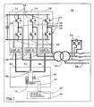
- a three-phase inverter 10 comprises three mutator modules 12, 14, 16 having identical structures, with coupling in parallel across the terminals of a capacitor 18, and of a direct current source.
- Each mutator 12,14,16 has two power transistors 20,22 connected in series, the collector of transistor 20 being electrically connected to the positive pole of the DC source, and the emitter of transistor 22 being connected to the negative pole.
- a protective diode 24 is mounted in reverse between the collector and the emitter of each transistor 20,22.
- the midpoint 26,28,30 arranged between the emitter of transistor 20 and the collector of transistor 22 of each module 12,14,16 is connected to the primary winding of a three-phase transformer 32.
- the receiver (not shown) is supplied by the active conductors L1, L2, L3, N connected to the secondary winding of the transformer 32 with the interposition of a cell of capacitors 34, and of a protective circuit breaker 36.
- Each mutator module 12,14,16 further comprises a power amplifier 38 connected to the bases of the transistors 20,22.
- the operation of the various modules 12, 14, 16 of the inverter 10 is controlled by an electronic control card 40, of the type described in French patent applications No. 8612963 and 8612962 of the applicant.
- a common mode inductor 42 In the electrical connection of the card 40 with the three power amplifiers 38, is inserted a common mode inductor 42, produced with a ribbon cable 44 or sheet of twenty six wires, wound on the central core of a single magnetic circuit 46 of rectangular shape ( Figure 4).
- One end of the ribbon cable 44 is equipped with a first connector intended to be plugged into a conjugate connector of the card 40.
- the other end carries a second connector 50 to which three strands of wires 52,54 are connected, 56 connected respectively to the power amplifiers 38 of the three modules 12,14,16.
- the 26 wires of the ribbon cable 44 represent the totality of the conductors relating to the commands and to the control information of the six power transistors 20, 24 of the modules 12, 14, 16.
- the intermediate part of the ribbon cable 44 wound on the magnetic circuit 46 forms the coil of the inductor 42, and the value of the reactance depends on the number of turns wound on the magnetic circuit 46.
- Each power of the inverter 10 corresponds to a predetermined value of the filtering inductor 42 to obtain optimum compensation for common mode disturbances affecting the control and monitoring conductors as a result of sudden potential variations generated during the conduction and blocking phases of the transistors 20,22.
- the magnetic circuit 46 is standard for all the values of the inductor 42, only the number of turns of the ribbon cable 44 on the central core changes.
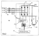
- a rectifier / charger module 60 comprises a three-phase Graetz bridge 62 equipped with six thyristors 64.
- the input of bridge 62 is connected to the alternating network with active conductors L1, L2, L3, by means of a switch 66 and fuses FU1, FU2, FU3.
- the output of bridge 62 is connected to the inverter 10 of FIG. 1, with a battery circuit 68 comprising a switch 70 and a resistor 72 in parallel.
- the triggers of the thyristors 64 of bridge 62 are electrically connected by conductors 73 to a power amplifier 74.
- the setting of the thyristor ignition angle for adjusting the output voltage of the bridge 62 is ensured by an electronic control card 76.
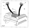
- the electrical connection between the card 76 and the power amplifier 74 is produced by means of a strand 78 with multiple wires 79, the part of which intermediate is wound around a magnetic circuit 80 to form a common mode inductor 82.
- the common mode inductor 82 is represented in FIG. 5, and the various wires 79 constituting the strand 78 are connected by their opposite ends to two connectors 84,86 intended to be inserted on the card 76 and the printed circuit of the amplifier 74.
- the coil 88 of the inductor 82 is formed by the helical winding of the strand 78 on the inner branch of the magnetic circuit 80. It is noted that the control links of the thyristors 64 of the rectifier / charger module 60 have been grouped in the same strand, itself wound around a common magnetic circuit 80 to constitute the common mode inductor 82.
- a static contactor module 90 is electrically inserted between a second alternative network (network 2), and the output of the inverter 10.
- the use is connected to the outputs of the inverter 10 and of the static contactor module 90 via a switch 92.
- a bypass circuit (BY-PASS) with circuit breaker 94 for commissioning, is connected directly in parallel between network 2 and the use for shunting the static contactor module 90.
- the static contactor module 90 comprises a pair of thyristors 96 at the top, or a triac in each active conductor L1, L2, L3 of the network 2.
- the triggers of the thyristors 96 are connected to a power amplifier 174 controlled by an electronic card of control 98.
- the card 98 is connected to an amplifier 174 by a strand link 178 and a common mode inductor 182 of the type illustrated in FIG. 5.
- all the power conductors 100, 102, 104 coming from the battery 68, from the 380 V network, and from a DC contactor control are formed, into a single strand 106 of 6 wires, electrically connected to a card supply 108, for example of the switching type.
- the part intermediate of the strand 106 is wound on a magnetic circuit 280 to constitute a common mode inductor 282 of the type illustrated in FIG. 5.
- the inductor 282 is included in the supply of energy to the power supply board 108.
- the conductors 110,112,114 power at the output of the power supply card 108 do not convey any common mode disturbance to the other electronic control cards 40,76,98.
- FIG. 7 shows an example of installation of the different common mode inductors 42,82,182,282 in an uninterruptible power supply system 120 having powers between 10 and 20 k VA.
- the architecture of the uninterruptible power supply 120 is described in detail in French patent applications No. 8617709 and 8617710 of the applicant, and the common mode inductors 42,82,182,282 have been arranged in the vicinity of the semiconductor modules of power and corresponding control cards.
Abstract
Description
L'invention est relative à un convertisseur statique de puissance, notamment pour un système d'alimentation sans coupure, comprenant un circuit de conversion ayant une pluralité de semi-conducteurs de puissance, une carte électronique de commande des semi-conducteurs du circuit de conversion, et des moyens d'alimentation électrique de la carte électronique de commande.The invention relates to a static power converter, in particular for an uninterruptible power supply system, comprising a conversion circuit having a plurality of power semiconductors, an electronic card for controlling the semiconductors of the conversion circuit. , and means for supplying power to the electronic control card.
Les problèmes rencontrés dans le fonctionnement d'un convertisseur statique concernent la transmission des informations de commande de l'électronique à bas niveau vers les semi-conducteurs de puissance du circuit de conversion, notamment les thyristors d'un chargeur de batterie, ou les transistors des mutateurs d'un onduleur. Les conducteurs véhiculant ces informations, subissent des perturbations de mode commun dues aux brusques variations de potentiel des semi-conducteurs qu'ils commandent, lorsque ces derniers deviennent conducteurs ou se bloquent. Ces perturbations peuvent affecter le fonctionnement des cartes électroniques de commande. Une solution pour minimiser l'influence de ces perturbations consiste à limiter la circulation du courant en insérant une bobine de compensation entre chaque semi-conducteur de puissance et les conducteurs de commande concernés de la carte électronique. L'inductance réalisée n'affecte pas la transmission des signaux utiles, mais s'oppose à la circulation des courants de même valeur instantanée sur deux fils.The problems encountered in the operation of a static converter relate to the transmission of control information from low-level electronics to the power semiconductors of the conversion circuit, in particular the thyristors of a battery charger, or the transistors. mutators of an inverter. The conductors carrying this information undergo common mode disturbances due to the sudden variations in potential of the semiconductors that they control, when the latter become conductors or become blocked. These disturbances can affect the operation of the electronic control cards. One solution to minimize the influence of these disturbances consists in limiting the flow of current by inserting a compensation coil between each power semiconductor and the relevant control conductors of the electronic card. The inductance carried out does not affect the transmission of useful signals, but opposes the circulation of currents of the same instantaneous value over two wires.
Il existe dans le commerce, une gamme importante de bobines à compensation de courant ayant des caractéristiques différentes en intensités de courant et en impédances. Ces bobines se présentent sous forme de composants individuels ayant des pattes de raccordement qui doivent être soudées dans le circuit. Un circuit de conversion d'un convertisseur statique possède un certain nombre de semi-conducteurs de puissance, et la gamme d'un système d'alimentation sans coupure présente d'autre part différents niveaux de puissance (par exemple 10 k VA, 20 k VA ... 80 k VA). A chaque puissance, et à chaque type de circuit de conversion, doit correspondre une impédance prédéterminée de la bobine de compensation. On remarque qu'une multitude de bobines de compensation seraient nécessaires pour obtenir une atténuation efficace des parasites engendrés par le fonctionnement du convertisseur. Le soudage individuel de ces bobines complique d'autre part la fabrication du convertisseur.There is a large range of current compensated coils on the market with different characteristics in current intensities and impedances. These coils are in the form of individual components having connection lugs which must be soldered in the circuit. A static converter conversion circuit has a certain number of power semiconductors, and the range of an uninterruptible power supply system also has different power levels (for example 10 k VA, 20 k VA ... 80 k VA). Each power, and each type of conversion circuit, must correspond to a predetermined impedance of the compensation coil. It is noted that a multitude of compensation coils would be necessary to obtain an effective attenuation of the parasites generated by the operation of the converter. The individual welding of these coils further complicates the manufacture of the converter.
L'objet de l'invention consite à simplifier l'opération de déparasitage d'un convertisseur statique de puissance.The object of the invention is to simplify the deworming operation of a static power converter.
Le convertisseur selon l'invention est caractérisé en ce que, la totalité des conducteurs de transmission d'informations de commande, et de surveillance entre la carte de commande, et le circuit de conversion est conformée en limande ou toron souple, dont la partie intermédiaire est enroulée sur un circuit magnétique unique pour constituer une inductance de mode commun, destinée à compenser les perturbations affectant la carte électronique par l'action des variations de potentiel des semi-conducteurs engendrées, lors du passage de l'état conducteur vers l'état bloqué, et vice-versa.The converter according to the invention is characterized in that, all of the conductors for transmitting control information and for monitoring between the control card and the conversion circuit is made of flounder or flexible strand, the intermediate part of which is wound on a single magnetic circuit to constitute a common mode inductor, intended to compensate for disturbances affecting the electronic card by the action of the potential variations of the semiconductors generated, during the transition from the conducting state to the state blocked, and vice versa.
A chaque carte de commande est associée une seule inductance de mode commun. Le circuit magnétique de l'inductance est standard pour toutes les puissances, la valeur de l'impédance étant ajustée par le nombre de spires de la limande ou du toron. La réalisation et l'insertion de l'inductance de mode commun s'effectue sans opération de soudage.A single common mode choke is associated with each control card. The magnetic circuit of the inductor is standard for all powers, the value of the impedance being adjusted by the number of turns of the ribbon cable or the strand. The realization and the insertion of the inductance of common mode is carried out without welding operation.
Les semi-conducteurs de puissance du circuit de conversion comportent des transistors ou des thyristors ayant un couplage prédéterminé pour définir, soit des modules mutateur d'un onduleur, soit un module redresseur-chargeur, soit un module contacteur statique, ayant chacun respectivement une carte de commande appropriée et une inductance de mode commun.The power semiconductors of the conversion circuit comprise transistors or thyristors having a predetermined coupling to define, either mutator modules of an inverter, or a rectifier-charger module, or a static contactor module, each having a card respectively. of appropriate control and a common mode inductor.
Les différentes cartes de commande desdits modules du système d'alimentation sans coupure sont alimentées par une carte d'alimentation commune. Les conducteurs de puissance en provenance de la batterie, du réseau alternatif, ou d'une commande auxiliaire sont conformés en un toron unique enroulé sur un circuit magnétique pour former une inductance de mode commun incluse dans la fourniture d'energie à la carte d'alimentation.The various control cards of said modules of the uninterruptible power supply system are supplied by a common power supply card. The power conductors from the battery, the AC network, or an auxiliary control are formed into a single strand wound on a magnetic circuit to form a common mode inductor included in the supply of energy to the card. food.
D'autres avantages et caractéristiques ressortiront plus clairement de la description qui va suivre de plusieurs modes de réalisation de l'invention, donnés à titre d'exemples non limitatifs et représentés aux dessins annexés dans lesquels:
- - la figure 1 représente le schéma d'un onduleur triphasé équipé de l'inductance de mode commun selon l'invention;
- - la figure 2 montre l'insertion de l'inductance de mode commun dans les commandes d'un redresseur-chargeur;
- - la figure 3 représente une variante appliquée à un contacteur statique.
- - la figure 4 représente une vue à échelle agrandie de l'inductance de mode commun utilisée dans le circuit de la figure 1;
- - la figure 5 est une variante de la figure 4, d'une inductance de mode commun utilisée dans les circuits des figures 2 et 3;
- - la figure 6 montre l'insertion d'une inductance de mode commun dans le circuit d'alimentation du convertisseur;
- - la figure 7 illustre l'implantation des différentes inductances de mode commun dans un système d'alimentation sans coupure.
- - Figure 1 shows the diagram of a three-phase inverter equipped with the common mode inductor according to the invention;
- - Figure 2 shows the insertion of the common mode inductor in the commands of a rectifier-charger;
- - Figure 3 shows a variant applied to a static contactor.
- - Figure 4 shows an enlarged view of the common mode inductor used in the circuit of Figure 1;
- - Figure 5 is a variant of Figure 4, of a common mode inductor used in the circuits of Figures 2 and 3;
- - Figure 6 shows the insertion of a common mode inductor in the converter supply circuit;
- - Figure 7 illustrates the implementation of the different common mode inductors in a power system without break.
En référence à la figure 1, un onduleur 10 triphasé comporte trois modules mutateurs 12,14,16 ayant des structures identiques, avec couplage en parallèle aux bornes d'un condensateur 18, et d'une source à courant continu. Chaque mutateur 12,14,16 comporte deux transistors de puissance 20,22 branchés en série, le collecteur du transistor 20 étant relié électriquement au pôle positif de la source à courant continu, et l'émetteur du transistor 22 étant connecté au pôle négatif. Une diode 24 de protection est montée en inverse entre le collecteur et l'émetteur de chaque transistor 20,22. Le point milieu 26,28,30 agencé entre l'émetteur du transistor 20 et le collecteur du transistor 22 de chaque module 12,14,16 est relié à l'enroulement primaire d'un transformateur 32 triphasé. Le récepteur (non représenté) est alimenté par les conducteurs actifs L1,L2,L3,N raccordés l'enroulement secondaire du transformateur 32 avec interposition d'une cellule de condensateurs 34, et d'un disjoncteur 36 de protection.With reference to FIG. 1, a three-
Chaque module mutateur 12,14,16 comporte de plus un amplificateur 38 de puissance connecté aux bases des transistors 20,22. Le fonctionnement des différents modules 12,14,16 de l'onduleur 10 est piloté par une carte électronique 40 de commande, du type décrit dans les demandes de brevets français n° 8612963 et 8612962 de la demanderesse.Each
Dans la liaison électrique de la carte 40 avec les trois amplificateurs de puissance 38, est insérée une inductance 42 de mode commun, réalisée avec une limande 44 ou nappe de vingt six fils, enroulée sur le noyau central d'un circuit magnétique 46 unique de forme rectangulaire (figure 4). L'une des extrémités de la limande 44 est équipée d'un premier connecteur destiné à s'enficher dans un connecteur conjugué de la carte 40. L'autre extrémité porte un deuxième connecteur 50 auquel se raccordent trois torons de fils 52,54,56 reliés respectivement aux amplificateurs de puissance 38 des trois modules 12,14,16.In the electrical connection of the
Les 26 fils de la limande 44 représentent la totalité des conducteurs relatifs aux commandes et aux informations de contrôle des six transistors de puissance 20,24 des modules 12,14,16. La partie intermédiaire de la limande 44 enroulée sur le circuit magnétique 46 forme la bobine de l'inductance 42, et la valeur de la réactance dépend du nombre de spires enroulées sur le circuit magnétique 46. A chaque puissance de l'onduleur 10 correspond une valeur prédéterminée de l'inductance 42 de filtrage pour obtenir une compensation optimum des perturbations de mode commun affectant les conducteurs de commande et de surveillance par suite des brusques variations de potentiel engendrées lors des phases de conduction et de blocage des transistors 20,22. Le circuit magnétique 46 est standard pour toutes les valeurs de l'inductance 42, seul change le nombre de spires de la limande 44 sur le noyau central. L'ncorporation de l'inductance 42 selon la figure 4 dans la liaison de la carte 40 avec les torons 52,54,56 s'effectue sans opération de soudage, la bobine de l'inductance 42 étant réalisée par l'enroulement de la limande 44 souple. Une seule inductance 42 de mode commun est suffisante pour la totalité des transistors 20,22 de l'onduleur 10 triphasé.The 26 wires of the
Selon la figure 2, un module redresseur/chargeur 60 comporte un pont de Graetz 62 triphasé équipé de six thyristors 64. L'entrée du pont 62 est raccordée au réseau alternatif à conducteurs actifs L1,L2,L3, par l'intermédiaire d'un interrupteur 66 et de fusibles FU1,FU2,FU3. La sortie du pont 62 est connectée à l'onduleur 10 de la figure 1, avec mise en parallèle d'un circuit à batterie 68 comprenant un interrupteur 70, et une résistance 72. Les gâchettes des thyristors 64 du pont 62 sont branchées électriquement par des conducteurs 73 à un amplificateur de puissance 74. Le réglage de l'angle d'amorçage des thyristors permettant d'ajuster la tension de sortie du pont 62 est assuré par une carte électronique de commande 76. La liaison électrique entre la carte 76 et l'amplificateur de puissance 74 est réalisée au moyen d'un toron 78 à fils 79 multiples, dont la partie intermédiaire est enroulée autour d'un circuit magnétique 80 pour former une inductance de mode commun 82.According to FIG. 2, a rectifier /
L'inductance de mode commun 82 est représentée sur la figure 5, et les différents fils 79 constitutifs du toron 78 sont raccordés par leurs extrémités opposées à deux connecteurs 84,86 destinés à être enfichés sur la carte 76 et le circuit imprimé de l'amplificateur 74. La bobine 88 de l'inductance 82 est formée par l'enroulement hélicoïdal du toron 78 sur la branche intérieure du circuit magnétique 80. On remarque que les liaisons de commande des thyristors 64 du module redresseur/chargeur 60 ont été regroupées dans un même toron, lui-même enroulé autour d'un circuit magnétique 80 commun pour constituer l'inductance de mode commun 82.The
Selon la figure 3, un module contacteur statique 90 est inséré électriquement entre un deuxième réseau alternatif (réseau 2), et la sortie de l'onduleur 10. L'utilisation est raccordée aux sorties de l'onduleur 10 et du module contacteur statique 90 par l'intermédiaire d'un interrupteur 92. Un circuit dérivé (BY-PASS) avec disjoncteur 94 de mise en service, est branché directement en parallèle entre le réseau 2 et l'utilisation pour shunter le module contacteur statique 90.According to FIG. 3, a
Le module contacteur statique 90 comprend une paire de thyristors 96 en tête bêche, ou un triac dans chaque conducteur actif L1,L2,L3 du réseau 2. Les gâchettes des thyristors 96 sont reliées à un amplificateur de puissance 174 piloté par une carte électronique de commande 98. La carte 98 est raccordée à un amplificateur 174 par une liaison à toron 178 et une inductance de mode commun 182 du type illustré à la figure 5.The
Sur la figure 6, tous les conducteurs 100,102,104 de puissance en provenance de la batterie 68, du réseau 380 V, et d'une commande contacteur à courant continu sont conformés, en un toron 106 unique de 6 fils, connecté électriquement à une carte d'alimentation 108, par exemple du type à découpage. La partie intermédiaire du toron 106 est bobinée sur un circuit magnétique 280 pour constituer une inductance de mode commun 282 du type illustré à la figure 5. L'inductance 282 se trouve incluse dans la fourniture d'énergie à la carte d'alimentation 108. Les conducteurs de puissance 110,112,114 à la sortie de la carte d'alimentation 108 ne véhiculent aucune perturbation de mode commun vers les autres cartes électroniques de commande 40,76,98.In FIG. 6, all the
La figure 7 montre un exemple d'implantation des différentes inductances de mode commun 42,82,182,282 dans un système d'alimentation sans coupure 120 ayant des puissances comprises entre 10 et 20 k VA. L'architecture de l'alimentation sans coupure 120 est décrite en détail dans les demandes de brevets français n° 8617709 et 8617710 de la demanderesse, et les inductances de mode commun 42,82,182,282 ont été disposées au voisinage des modules à semi-conducteurs de puissance et des cartes de commande correspondantes.FIG. 7 shows an example of installation of the different
Claims (4)
Applications Claiming Priority (2)
| Application Number | Priority Date | Filing Date | Title |
|---|---|---|---|
| FR8710521A FR2618617B1 (en) | 1987-07-23 | 1987-07-23 | DEVICE FOR FILTERING COMMON MODE DISTURBANCES AFFECTING THE CARDS OF A STATIC POWER CONVERTER |
| FR8710521 | 1987-07-23 |
Publications (3)
| Publication Number | Publication Date |
|---|---|
| EP0300872A1 true EP0300872A1 (en) | 1989-01-25 |
| EP0300872B1 EP0300872B1 (en) | 1992-12-09 |
| EP0300872B2 EP0300872B2 (en) | 1996-05-15 |
Family
ID=9353527
Family Applications (1)
| Application Number | Title | Priority Date | Filing Date |
|---|---|---|---|
| EP88401773A Expired - Lifetime EP0300872B2 (en) | 1987-07-23 | 1988-07-07 | Filtering device for common types disturbances acting on a static power converter's electronic cards |
Country Status (5)
| Country | Link |
|---|---|
| US (1) | US4903185A (en) |
| EP (1) | EP0300872B2 (en) |
| DE (1) | DE3876526T2 (en) |
| ES (1) | ES2037856T5 (en) |
| FR (1) | FR2618617B1 (en) |
Cited By (3)
| Publication number | Priority date | Publication date | Assignee | Title |
|---|---|---|---|---|
| WO1990009695A1 (en) * | 1989-02-17 | 1990-08-23 | Europe Patent Limited | A device with a multi-phase load, a static converter and choke coils |
| EP0469255A1 (en) * | 1990-07-31 | 1992-02-05 | Tandberg Data A/S | Electrostatic discharge noise suppression method and system for electronic device |
| EP0497631A2 (en) * | 1991-01-31 | 1992-08-05 | International Business Machines Corporation | Transformer with capacitive current suppresion |
Families Citing this family (5)
| Publication number | Priority date | Publication date | Assignee | Title |
|---|---|---|---|---|
| US5936856A (en) * | 1998-02-13 | 1999-08-10 | Baldor Electric Companh | Method and apparatus for active common-mode voltage compensation in induction motor systems |
| DE10142737B4 (en) * | 2001-08-28 | 2007-02-15 | Pilz Gmbh & Co. Kg | Safety switching device, in particular for safe shutdown of industrial machinery |
| US7312101B2 (en) * | 2003-04-22 | 2007-12-25 | Micron Technology, Inc. | Packaged microelectronic devices and methods for packaging microelectronic devices |
| DE102006050289B4 (en) * | 2006-10-23 | 2015-11-12 | Rittal Gmbh & Co. Kg | Power supply means |
| EP2299582B1 (en) | 2009-09-18 | 2015-03-11 | SMA Solar Technology AG | Inverter with a housing and electric and electronic components assembled within same |
Citations (2)
| Publication number | Priority date | Publication date | Assignee | Title |
|---|---|---|---|---|
| US4259705A (en) * | 1979-03-27 | 1981-03-31 | Stifter Francis J | Combination surge suppressor filter |
| US4636752A (en) * | 1984-06-08 | 1987-01-13 | Murata Manufacturing Co., Ltd. | Noise filter |
Family Cites Families (4)
| Publication number | Priority date | Publication date | Assignee | Title |
|---|---|---|---|---|
| US3388351A (en) * | 1964-02-14 | 1968-06-11 | Westinghouse Electric Corp | Foil or strip inductor device |
| US3551858A (en) * | 1967-06-14 | 1970-12-29 | Ibm | High current feed-through filter system |
| JPS54144851A (en) * | 1978-05-02 | 1979-11-12 | Matsushita Electric Ind Co Ltd | Noise filter |
| US4760355A (en) * | 1985-11-04 | 1988-07-26 | Glen Dash | Electromagnetic emission control system |
-
1987
- 1987-07-23 FR FR8710521A patent/FR2618617B1/en not_active Expired
-
1988
- 1988-07-07 ES ES88401773T patent/ES2037856T5/en not_active Expired - Lifetime
- 1988-07-07 EP EP88401773A patent/EP0300872B2/en not_active Expired - Lifetime
- 1988-07-07 DE DE3876526T patent/DE3876526T2/en not_active Expired - Fee Related
- 1988-07-13 US US07/218,262 patent/US4903185A/en not_active Expired - Fee Related
Patent Citations (2)
| Publication number | Priority date | Publication date | Assignee | Title |
|---|---|---|---|---|
| US4259705A (en) * | 1979-03-27 | 1981-03-31 | Stifter Francis J | Combination surge suppressor filter |
| US4636752A (en) * | 1984-06-08 | 1987-01-13 | Murata Manufacturing Co., Ltd. | Noise filter |
Non-Patent Citations (1)
| Title |
|---|
| PATENT ABSTRACTS OF JAPAN, vol. 4, no. 4 (E-164), 12 janvier 1980, page 133 E 164; & JP-A-54 144 851 (MATSUSHITA DENKI SANGYO K.K.) 12-11-1979 * |
Cited By (5)
| Publication number | Priority date | Publication date | Assignee | Title |
|---|---|---|---|---|
| WO1990009695A1 (en) * | 1989-02-17 | 1990-08-23 | Europe Patent Limited | A device with a multi-phase load, a static converter and choke coils |
| EP0469255A1 (en) * | 1990-07-31 | 1992-02-05 | Tandberg Data A/S | Electrostatic discharge noise suppression method and system for electronic device |
| US5287008A (en) * | 1990-07-31 | 1994-02-15 | Tandberg Data A/S | Electrostatic discharge noise suppression method and system for electronic devices |
| EP0497631A2 (en) * | 1991-01-31 | 1992-08-05 | International Business Machines Corporation | Transformer with capacitive current suppresion |
| EP0497631A3 (en) * | 1991-01-31 | 1993-03-10 | International Business Machines Corporation | Transformer with capacitive current suppresion |
Also Published As
| Publication number | Publication date |
|---|---|
| ES2037856T3 (en) | 1993-07-01 |
| DE3876526D1 (en) | 1993-01-21 |
| FR2618617B1 (en) | 1989-11-17 |
| EP0300872B1 (en) | 1992-12-09 |
| DE3876526T2 (en) | 1996-11-28 |
| US4903185A (en) | 1990-02-20 |
| EP0300872B2 (en) | 1996-05-15 |
| ES2037856T5 (en) | 1996-10-01 |
| FR2618617A1 (en) | 1989-01-27 |
Similar Documents
| Publication | Publication Date | Title |
|---|---|---|
| US4890089A (en) | Distribution of line carrier communications | |
| US5081440A (en) | Bus coupler | |
| US11728845B2 (en) | Variable impedance circuit | |
| JPS58114561A (en) | Communication system | |
| US5841205A (en) | Branching unit for underwater telecommunications systems | |
| US4755922A (en) | DC to DC converter for ethernet transceiver | |
| EP0300872B1 (en) | Filtering device for common types disturbances acting on a static power converter's electronic cards | |
| FR2468193A1 (en) | TRANSFORMER, PARTICULARLY USEFUL AS A SWITCHING REGULATOR | |
| KR950015094B1 (en) | Line interface circuit | |
| CN1009980B (en) | Static transducer containing filter against high-frequency interference | |
| EP0185876A2 (en) | An fet switch for high frequency signals | |
| FR2665309A1 (en) | SEMICONDUCTOR CONTROL APPARATUS. | |
| CA2104633C (en) | Active filter for a traction motor supplied from a single-phase catenary | |
| EP0301923A1 (en) | Electric power supply, especially for a wave generator of a pulse radar | |
| US4238644A (en) | Supply circuit for a subscriber's line circuit | |
| US4771229A (en) | Circuit arrangement for automatic connection of the remote feed current paths of a remote feed loop | |
| EP1220468B1 (en) | Submarine cable branching unit with current limiter | |
| US6765775B2 (en) | Submarine cable branching unit with current limiter | |
| JPS60237751A (en) | Line power supplying circuit and energizing current supplying method | |
| JPH05129991A (en) | Feeder changeover circuit | |
| US11870506B2 (en) | Power-line/communication system | |
| US3974345A (en) | Negative impedance repeater with double amplification, for telephone lines | |
| US4580187A (en) | A-C current limiting device | |
| EP0250334B1 (en) | Interface for connecting a device to a coaxial cable | |
| US5253290A (en) | Circuit arrangement for the transmission of telecommunication signals |
Legal Events
| Date | Code | Title | Description |
|---|---|---|---|
| PUAI | Public reference made under article 153(3) epc to a published international application that has entered the european phase |
Free format text: ORIGINAL CODE: 0009012 |
|
| AK | Designated contracting states |
Kind code of ref document: A1 Designated state(s): BE CH DE ES GB IT LI NL SE |
|
| 17P | Request for examination filed |
Effective date: 19890623 |
|
| 17Q | First examination report despatched |
Effective date: 19920205 |
|
| GRAA | (expected) grant |
Free format text: ORIGINAL CODE: 0009210 |
|
| AK | Designated contracting states |
Kind code of ref document: B1 Designated state(s): BE CH DE ES GB IT LI NL SE |
|
| PG25 | Lapsed in a contracting state [announced via postgrant information from national office to epo] |
Ref country code: NL Effective date: 19921209 Ref country code: SE Effective date: 19921209 |
|
| REF | Corresponds to: |
Ref document number: 3876526 Country of ref document: DE Date of ref document: 19930121 |
|
| ITF | It: translation for a ep patent filed |
Owner name: EUROPATENT S.A.S. |
|
| GBT | Gb: translation of ep patent filed (gb section 77(6)(a)/1977) |
Effective date: 19930312 |
|
| NLV1 | Nl: lapsed or annulled due to failure to fulfill the requirements of art. 29p and 29m of the patents act | ||
| REG | Reference to a national code |
Ref country code: ES Ref legal event code: FG2A Ref document number: 2037856 Country of ref document: ES Kind code of ref document: T5 |
|
| PG25 | Lapsed in a contracting state [announced via postgrant information from national office to epo] |
Ref country code: CH Effective date: 19930731 Ref country code: LI Effective date: 19930731 Ref country code: BE Effective date: 19930731 |
|
| PLBI | Opposition filed |
Free format text: ORIGINAL CODE: 0009260 |
|
| 26 | Opposition filed |
Opponent name: SIEMENS AG Effective date: 19930906 |
|
| BERE | Be: lapsed |
Owner name: MERLIN GERIN Effective date: 19930731 |
|
| REG | Reference to a national code |
Ref country code: CH Ref legal event code: PL |
|
| PUAH | Patent maintained in amended form |
Free format text: ORIGINAL CODE: 0009272 |
|
| STAA | Information on the status of an ep patent application or granted ep patent |
Free format text: STATUS: PATENT MAINTAINED AS AMENDED |
|
| 27A | Patent maintained in amended form |
Effective date: 19960515 |
|
| AK | Designated contracting states |
Kind code of ref document: B2 Designated state(s): BE CH DE ES GB IT LI NL SE |
|
| REG | Reference to a national code |
Ref country code: CH Ref legal event code: AEN Free format text: MAINTIEN DU BREVET DONT L'ETENDUE A ETE MODIFIEE |
|
| GBTA | Gb: translation of amended ep patent filed (gb section 77(6)(b)/1977) |
Effective date: 19960710 |
|
| ITF | It: translation for a ep patent filed |
Owner name: EUROPATENT S.A.S. |
|
| REG | Reference to a national code |
Ref country code: ES Ref legal event code: DC2A Kind code of ref document: T5 Effective date: 19960812 |
|
| REG | Reference to a national code |
Ref country code: ES Ref legal event code: DC2A Kind code of ref document: T5 Effective date: 19960812 |
|
| REG | Reference to a national code |
Ref country code: GB Ref legal event code: IF02 |
|
| PGFP | Annual fee paid to national office [announced via postgrant information from national office to epo] |
Ref country code: ES Payment date: 20040719 Year of fee payment: 17 |
|
| PGFP | Annual fee paid to national office [announced via postgrant information from national office to epo] |
Ref country code: GB Payment date: 20050706 Year of fee payment: 18 |
|
| PG25 | Lapsed in a contracting state [announced via postgrant information from national office to epo] |
Ref country code: ES Free format text: LAPSE BECAUSE OF NON-PAYMENT OF DUE FEES Effective date: 20050708 |
|
| PGFP | Annual fee paid to national office [announced via postgrant information from national office to epo] |
Ref country code: DE Payment date: 20050711 Year of fee payment: 18 |
|
| PG25 | Lapsed in a contracting state [announced via postgrant information from national office to epo] |
Ref country code: GB Free format text: LAPSE BECAUSE OF NON-PAYMENT OF DUE FEES Effective date: 20060707 |
|
| PGFP | Annual fee paid to national office [announced via postgrant information from national office to epo] |
Ref country code: IT Payment date: 20060731 Year of fee payment: 19 |
|
| REG | Reference to a national code |
Ref country code: ES Ref legal event code: FD2A Effective date: 20050708 |
|
| PG25 | Lapsed in a contracting state [announced via postgrant information from national office to epo] |
Ref country code: DE Free format text: LAPSE BECAUSE OF NON-PAYMENT OF DUE FEES Effective date: 20070201 |
|
| GBPC | Gb: european patent ceased through non-payment of renewal fee |
Effective date: 20060707 |
|
| PG25 | Lapsed in a contracting state [announced via postgrant information from national office to epo] |
Ref country code: IT Free format text: LAPSE BECAUSE OF NON-PAYMENT OF DUE FEES Effective date: 20070707 |