EP0321087A1 - Anti-reflection coatings - Google Patents
Anti-reflection coatings Download PDFInfo
- Publication number
- EP0321087A1 EP0321087A1 EP88310495A EP88310495A EP0321087A1 EP 0321087 A1 EP0321087 A1 EP 0321087A1 EP 88310495 A EP88310495 A EP 88310495A EP 88310495 A EP88310495 A EP 88310495A EP 0321087 A1 EP0321087 A1 EP 0321087A1
- Authority
- EP
- European Patent Office
- Prior art keywords
- coating
- facet
- coatings
- refractive index
- hafnium oxide
- Prior art date
- Legal status (The legal status is an assumption and is not a legal conclusion. Google has not performed a legal analysis and makes no representation as to the accuracy of the status listed.)
- Withdrawn
Links
- 238000000576 coating method Methods 0.000 title claims abstract description 70
- 229910000449 hafnium oxide Inorganic materials 0.000 claims abstract description 19
- WIHZLLGSGQNAGK-UHFFFAOYSA-N hafnium(4+);oxygen(2-) Chemical compound [O-2].[O-2].[Hf+4] WIHZLLGSGQNAGK-UHFFFAOYSA-N 0.000 claims abstract description 18
- QVGXLLKOCUKJST-UHFFFAOYSA-N atomic oxygen Chemical compound [O] QVGXLLKOCUKJST-UHFFFAOYSA-N 0.000 claims abstract description 12
- 229910052760 oxygen Inorganic materials 0.000 claims abstract description 12
- 239000001301 oxygen Substances 0.000 claims abstract description 12
- 239000004065 semiconductor Substances 0.000 claims abstract description 10
- 230000003287 optical effect Effects 0.000 claims abstract description 9
- 239000011248 coating agent Substances 0.000 claims description 44
- 238000000151 deposition Methods 0.000 claims description 10
- 238000012856 packing Methods 0.000 claims description 9
- 239000000463 material Substances 0.000 claims description 6
- 230000005855 radiation Effects 0.000 claims description 6
- 229910052738 indium Inorganic materials 0.000 claims description 4
- 238000000034 method Methods 0.000 claims description 4
- 229910052785 arsenic Inorganic materials 0.000 claims description 3
- 230000005540 biological transmission Effects 0.000 claims description 3
- 229910052733 gallium Inorganic materials 0.000 claims description 3
- 229910052698 phosphorus Inorganic materials 0.000 claims description 3
- 229910005540 GaP Inorganic materials 0.000 claims 1
- GPXJNWSHGFTCBW-UHFFFAOYSA-N Indium phosphide Chemical compound [In]#P GPXJNWSHGFTCBW-UHFFFAOYSA-N 0.000 claims 1
- HZXMRANICFIONG-UHFFFAOYSA-N gallium phosphide Chemical compound [Ga]#P HZXMRANICFIONG-UHFFFAOYSA-N 0.000 claims 1
- APFVFJFRJDLVQX-UHFFFAOYSA-N indium atom Chemical compound [In] APFVFJFRJDLVQX-UHFFFAOYSA-N 0.000 claims 1
- 230000005693 optoelectronics Effects 0.000 claims 1
- 230000008021 deposition Effects 0.000 abstract description 8
- 230000003647 oxidation Effects 0.000 abstract description 8
- 238000007254 oxidation reaction Methods 0.000 abstract description 8
- 239000010410 layer Substances 0.000 description 9
- 230000010355 oscillation Effects 0.000 description 8
- 238000002310 reflectometry Methods 0.000 description 8
- 239000011148 porous material Substances 0.000 description 5
- 239000013078 crystal Substances 0.000 description 4
- 229920006395 saturated elastomer Polymers 0.000 description 4
- 239000000758 substrate Substances 0.000 description 4
- XLYOFNOQVPJJNP-UHFFFAOYSA-N water Substances O XLYOFNOQVPJJNP-UHFFFAOYSA-N 0.000 description 4
- 230000000694 effects Effects 0.000 description 3
- 230000003321 amplification Effects 0.000 description 2
- 238000003199 nucleic acid amplification method Methods 0.000 description 2
- 229910052688 Gadolinium Inorganic materials 0.000 description 1
- 229910000530 Gallium indium arsenide Inorganic materials 0.000 description 1
- 229910052779 Neodymium Inorganic materials 0.000 description 1
- KXNLCSXBJCPWGL-UHFFFAOYSA-N [Ga].[As].[In] Chemical compound [Ga].[As].[In] KXNLCSXBJCPWGL-UHFFFAOYSA-N 0.000 description 1
- 230000002238 attenuated effect Effects 0.000 description 1
- 239000011247 coating layer Substances 0.000 description 1
- 150000001875 compounds Chemical class 0.000 description 1
- 238000010894 electron beam technology Methods 0.000 description 1
- 238000002474 experimental method Methods 0.000 description 1
- 239000000835 fiber Substances 0.000 description 1
- CJNBYAVZURUTKZ-UHFFFAOYSA-N hafnium(IV) oxide Inorganic materials O=[Hf]=O CJNBYAVZURUTKZ-UHFFFAOYSA-N 0.000 description 1
- 238000010438 heat treatment Methods 0.000 description 1
- 239000012535 impurity Substances 0.000 description 1
- 239000013307 optical fiber Substances 0.000 description 1
- 238000006213 oxygenation reaction Methods 0.000 description 1
- 230000002035 prolonged effect Effects 0.000 description 1
- 239000010453 quartz Substances 0.000 description 1
- 229910052710 silicon Inorganic materials 0.000 description 1
- VYPSYNLAJGMNEJ-UHFFFAOYSA-N silicon dioxide Inorganic materials O=[Si]=O VYPSYNLAJGMNEJ-UHFFFAOYSA-N 0.000 description 1
- 229910052727 yttrium Inorganic materials 0.000 description 1
Images
Classifications
-
- H—ELECTRICITY
- H01—ELECTRIC ELEMENTS
- H01L—SEMICONDUCTOR DEVICES NOT COVERED BY CLASS H10
- H01L33/00—Semiconductor devices with at least one potential-jump barrier or surface barrier specially adapted for light emission; Processes or apparatus specially adapted for the manufacture or treatment thereof or of parts thereof; Details thereof
- H01L33/44—Semiconductor devices with at least one potential-jump barrier or surface barrier specially adapted for light emission; Processes or apparatus specially adapted for the manufacture or treatment thereof or of parts thereof; Details thereof characterised by the coatings, e.g. passivation layer or anti-reflective coating
-
- G—PHYSICS
- G02—OPTICS
- G02B—OPTICAL ELEMENTS, SYSTEMS OR APPARATUS
- G02B1/00—Optical elements characterised by the material of which they are made; Optical coatings for optical elements
- G02B1/10—Optical coatings produced by application to, or surface treatment of, optical elements
- G02B1/11—Anti-reflection coatings
- G02B1/113—Anti-reflection coatings using inorganic layer materials only
-
- H—ELECTRICITY
- H01—ELECTRIC ELEMENTS
- H01L—SEMICONDUCTOR DEVICES NOT COVERED BY CLASS H10
- H01L31/00—Semiconductor devices sensitive to infrared radiation, light, electromagnetic radiation of shorter wavelength or corpuscular radiation and specially adapted either for the conversion of the energy of such radiation into electrical energy or for the control of electrical energy by such radiation; Processes or apparatus specially adapted for the manufacture or treatment thereof or of parts thereof; Details thereof
- H01L31/02—Details
- H01L31/0216—Coatings
-
- H—ELECTRICITY
- H01—ELECTRIC ELEMENTS
- H01S—DEVICES USING THE PROCESS OF LIGHT AMPLIFICATION BY STIMULATED EMISSION OF RADIATION [LASER] TO AMPLIFY OR GENERATE LIGHT; DEVICES USING STIMULATED EMISSION OF ELECTROMAGNETIC RADIATION IN WAVE RANGES OTHER THAN OPTICAL
- H01S5/00—Semiconductor lasers
- H01S5/02—Structural details or components not essential to laser action
- H01S5/028—Coatings ; Treatment of the laser facets, e.g. etching, passivation layers or reflecting layers
Definitions
- This invention relates to anti-reflection coatings and in particular to anti-reflection coatings for semiconductor laser devices, eg optical amplifiers.
- anti-reflection coatings in laser devices is well established. Some devices, eg distributed feedback lasers (usually called DFB lasers) and external cavity lasers, require a single anti-reflection coating. Other devices, eg optical amplifiers, require two anti-reflection coatings. Although these devices, and the use of anti-reflection coatings therein, are well established a brief description will be given.
- DFB lasers distributed feedback lasers
- optical amplifiers require two anti-reflection coatings.
- a DFB laser comprises an active semiconductor region in which an optical signal is generated.
- the DFB laser also includes a resonance system which has two components, namely a reflective facet, ideally 100% reflective, which is located at one end of the active region and a diffraction grating which provides wavelength selectivity.
- the active region also has an exit facet through which the radiation generated in the active region passes as output. Reflections from the exit facet are unwanted because the reflected radiation participates in the generation of radiation but the wavelength differs from that of the main signal. Thus it is desirable to apply an anti-reflection coating to the exit facet.
- An external cavity laser comprises an active semiconductor region in which the signal is generated and a separate cavity which is part of a resonant system.
- An optical amplifier also has an active region in which the lasing activity occurs but, because oscillation is highly undesirable, there is no resonance system.
- One form of amplifier hereinafter called a single pass amplifier, has an input facet for receiving weak optical signals, eg signals attenuated after long distance transmission.
- the amplifier also has an output facet through which signals, after amplification by passage through the active region, leave, eg for further transmission. Reflections at the input and output facets degrade the performance, eg by causing oscillation or noise. It is, therefore, conventional to apply anti-reflection coatings to both the input and output facets.
- one facet serves for both input and output.
- amplifiers are associated with directional couplers to separate input and output signals.
- the signal passes twice through the active region and the decibel gain is doubled.
- the input/output facet is provided with an anti-reflection coating but the other facet needs a mirror coating with a high, ideally 100%, reflectivity.
- the active region is formed of a semiconductor which contains at least one of Ga and In and at least one of P and As, eg mixed compounds of the formula Ga x In (1-x) As y P (1-y) where x is in the range 0.2 to 0.4 and y is in the range 0.5 to 0.9.
- a semiconductor which contains at least one of Ga and In and at least one of P and As, eg mixed compounds of the formula Ga x In (1-x) As y P (1-y) where x is in the range 0.2 to 0.4 and y is in the range 0.5 to 0.9.
- oxides have been proposed for this purpose, eg oxides of Y, Gd, Nd and Si. Indeed very low reflectivities have been achieved, eg of the order 10 ⁇ 4, but other factors have also to be taken into account, eg the stability of the coating. The ease and reproducability with which the coating may be deposited is also important. It is an object of this invention to provide coatings which have acceptably low levels of reflectivity, adequate stability and which can be deposited reproducably.
- the coatings are preferably 180 to 220nm thick.
- hafnium oxide exists in non-stoichiometric forms. Thus it can be represented by the formula HfO n where n is slightly less than 2. It is not possible to ascertain the value of n in a coating layer but the refractive index of the coating is related to its degree of oxidation. The refractive index is also related to the occurrence of voids within the coating. Thus it is desirable that the coating should have a refractive index, measured at 632.8nm, in the range 1.87 to 2.00 and a packing density in the range 0.86 to 0.96. The method of determining the packing density will be given below.
- the coatings according to the invention are conveniently produced by deposition from the vapour phase in the presence of oxygen at low pressure, eg below 10 ⁇ 3mbar. It is preferred to deposit the coating at a rate of 0.1 to 1nm/s preferably 0.2nm/s, under an oxygen pressure of between 1 and 5 x 10 ⁇ 4mbar.
- a target comprising 20 to 50 devices. After coating the target is cut into separate devices and electrical connectors are attached. Optical fibre may also be attached.
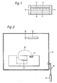
- the amplifier comprises a substrate 10 of InP.
- the substrate performs no function in the finished device. It provides support for the other layers which were grown onto the substrate.
- the operative layers are confining layers 11 and 12 which are formed of p and n type InP respectively.
- the active layer 13 an indium gallium arsenide phosphide semiconductor, is located between the confining layers 11 and 12.
- the active layer 13 has a higher refractive index than the two confining layers.
- the two end facets of the amplifier are coated with anti-reflection coatings 14 and 15 formed of hafnium oxide having a refractive index of 1.87 to 2.00 and a packing density of 0.91. (Note the refractive index range 1.87 to 2.00 applies when the index is measured with radiation of wavelength 632.8nm. If measured at the wavelength of use, eg 1.55 ⁇ m, the preferred refractive index is 1.84).
- the performance of these anti-reflection coatings is matched to the properties of the active layer 13.
- the hafnium oxide can not only suppress the lasing but substantially reduce this noise. For gains of over 20dB reflectivities below 0.5%, preferably below 0.2%, are appropriate. For gains of 30dB even lower reflectivities, eg below 0.05%, would be needed.
- the anti-reflection coatings according to the invention are applied using a conventional vapour deposition apparatus.
- the apparatus shown in Figure 2 comprises a vacuum chamber 19 which is connected to evacuation pumps (not shown).
- the chamber 19 contains the target 20 and a source 21 which is a hafnium oxide contained in a suitable crucible.
- the target 20 is heated to 300°C.
- the source is heated and thereby caused to evaporate by an electron beam 23 which is generated by an electron gun 22.
- a magnetic field (the mode of generation is not shown) is applied to cause the electrons to follow a curved path to impinge on the source 21. Varying the field causes the point of impact to wander so that hafnium oxide is evaporated from different parts of the source. Thus source material is evaporated so that it rises to deposit on target 20.
- the vacuum chamber 19 contains an atmosphere of oxgyen at a pressure between 1x10 ⁇ 4 and 5 x 10 ⁇ 4 mbar.
- oxygen is continuously leaked into the chamber 19 from a cylinder 25 via a leak valve 26.
- the evacuation pumps run continuously and the rate of supply of oxygen is adjusted so that the pressure is steady at the selected value. (Before adding any oxygen, the chamber 19 is evacuated to about 5 x 10 ⁇ 9mbar. Thus the oxygen atmosphere is substantially pure).
- the chamber 19 also contains a piezo-electric crystal 24 which is adjacent to the target 20 so that hafnium oxide deposits on both simultaneously.
- the frequency of oscillation of the crystal 24 is affected by the deposit.
- the crystal is calibrated in known manner and its frequency of oscillation is continuously monitored during deposition whereby the thickness and rate of growth are continuously available.
- the final thickness of the coating should be about 0.25 to 0.27, preferably 0.26, of a wavelength (as measured inside the coating) of the intended signals. (Note. If the wavelength of the intended signals is measured in vacuo the thickness is 0.12 to 0.14 of the wavelength). Thus for signals with wavelengths of 1.3 ⁇ m to 1.5 ⁇ m in vacuo, coating thicknesses of about 186nm to 220nm are suitable. We recommend about 186nm for 1.3 ⁇ m and 215 for 1.5 ⁇ m. The quartz crystal 24 detects the end point when the coating on the target has achieved the appropriate thickness.
- targets which contain several devices, eg about 30 devices, at one time. After coating (both facets) the target is cut into individual devices which are mounted for use. During coating the target is held in a conventional holder.
- oxygenated coatings of hafnium oxide were applied to semiconductor devices.
- hafnium oxide is substantially affected by the conditions under which it was deposited and conditions which favour substantially complete oxygenation appear to favour the lowest (most desirable) reflectivities.
- oxygen in the vacuum chamber 19 appears to exert a disadvantageous effect on the other properties of the coating, eg the coating may be slightly porous and hence its refractive index may change after deposition.
- the coating In order to take account of both effects we prefer to deposit the coating slowly, eg at a rate of less than 2nm/s, eg 0.1 to 1 nm/s, under a low oxygen pressure, eg 2 to 5x10 ⁇ 4mbar.
- the degree of oxidation can be measured by the refractive index of the coating and the target values are 1.87 to 2.00 measured at 632.8nm.
- the degree of porosity can be measured by the change of refractive index after very prolonged storage in air saturated with water vapour at 25°C.
- N H is measured first and the sample is dried, eg by heating at 300°C for 30 minutes in vacuo, and N o is measured second.
- a target in the form of a strip of 30 devices designed for operation at 1.5 ⁇ m was heated to 300°C and exposed to hafnium oxide vapour in the presence of oxygen at 3.4x10 ⁇ 4mbar.
- a coating 218nm thick was grown at 1.0nm/s. The target was treated twice so that two facets were coated.
- the refractive index was 1.941 and after saturation with water vapour (by exposure to saturated air for 3000 hrs at 30°C) the index rose to 1.971. This implies a packing density of 0.91 and that the refractive index of the hafnium oxide itself was 2.035. (All the refractive indices were measured at wavelength 632.8nm).
- the strip of 30 devices was cut into individual amplifiers and a gain of 28dB was achieved without oscillation. This implies a reflectivity below 0.2% for the coatings.
- a target in the form of a strip of 30 devices designed for operation at 1.5 ⁇ m was heated to 300°C and exposed to hafnium oxide vapour in the presence of oxygen at 3.1x10 ⁇ 4mbar.
- a coating 182nm thick was grown at 0.2nm/s. The target was treated twice so that two facets were coated.
- the refractive index was 1.916 and after saturation with water vapour (by exposure to saturated air at 30°C) the index rose to 1.943. This implies a packing density of 0.915 and that the refractive index of the hafnium oxide itself was 2.000.
- the strip of 30 devices was cut into individual amplifiers and a gain of 28dB was achieved without oscillation. This implies a reflectivity below 0.2% for the coatings.
- Examples 1 and 2 describe coatings wherein the hafnium oxide itself has a refractive index of 2.034 and 2.000 respectively.
- the value 2.034 is above the target range of 2.00 to 1.87 whereas the value 2.000 is at the top end of the range. Since the refractive index tends to decrease as the degree of oxidation increases, it appears that the oxidation conditions employed in Example 2 are more efficatious.
- the deposition methods also produce pores in the coatings and the presence of the pores reduces the refractive index.
- the pores provide a valuable control in reducing the refractive index to values which would be difficult to achieve by oxidation.
- the coating as a whole has a refractive index of 1.916 (because the packing density is 0.915) and this lower value is better than the "oxide" value of 2.000.
- the pores also represent a source of instability because impurities, eg water vapour, can diffuse into them.
- impurities eg water vapour
- this is not a serious disadvantage because the amplifier is encapsulated during use and in any case the total volume of the pores is small when the packing density is greater than 0.9.
- the fibres are placed close to the coatings so that the actual interface is air/hafnium oxide.
- the encapsulating material surrounds the ends of the fibre and the amplifier and it does not intrude into the path of the radiation.
Abstract
Optical devices, e.g. amplifiers, include anti-reflection coatings of hafnium oxide. The coatings are obtained by low temperature deposition in the presence of oxygen. It is important to adjust the degree of oxidation in order to obtain the target refractive index. Slower rates of deposition and oxidation favour stability of performance parameters. The coatings are useful for application to GaInAsP semiconductors.
Description
- This invention relates to anti-reflection coatings and in particular to anti-reflection coatings for semiconductor laser devices, eg optical amplifiers.
- The use of anti-reflection coatings in laser devices is well established. Some devices, eg distributed feedback lasers (usually called DFB lasers) and external cavity lasers, require a single anti-reflection coating. Other devices, eg optical amplifiers, require two anti-reflection coatings. Although these devices, and the use of anti-reflection coatings therein, are well established a brief description will be given.
- A DFB laser comprises an active semiconductor region in which an optical signal is generated. The DFB laser also includes a resonance system which has two components, namely a reflective facet, ideally 100% reflective, which is located at one end of the active region and a diffraction grating which provides wavelength selectivity. The active region also has an exit facet through which the radiation generated in the active region passes as output. Reflections from the exit facet are unwanted because the reflected radiation participates in the generation of radiation but the wavelength differs from that of the main signal. Thus it is desirable to apply an anti-reflection coating to the exit facet.
- An external cavity laser comprises an active semiconductor region in which the signal is generated and a separate cavity which is part of a resonant system. There is an internal facet between the active region and the cavity and reflections from the internal facet, not being tuned to the same wavelength as the resonance system, degrade performance. Thus it is desirable to apply anti-reflection coatings to the internal facet.
- An optical amplifier also has an active region in which the lasing activity occurs but, because oscillation is highly undesirable, there is no resonance system. One form of amplifier, hereinafter called a single pass amplifier, has an input facet for receiving weak optical signals, eg signals attenuated after long distance transmission. The amplifier also has an output facet through which signals, after amplification by passage through the active region, leave, eg for further transmission. Reflections at the input and output facets degrade the performance, eg by causing oscillation or noise. It is, therefore, conventional to apply anti-reflection coatings to both the input and output facets.
- In an alternative form of amplifier, hereinafter called a double pass amplifier, one facet serves for both input and output. In use such amplifiers are associated with directional couplers to separate input and output signals. In these amplifiers the signal passes twice through the active region and the decibel gain is doubled. The input/output facet is provided with an anti-reflection coating but the other facet needs a mirror coating with a high, ideally 100%, reflectivity.
- In many devices the active region is formed of a semiconductor which contains at least one of Ga and In and at least one of P and As, eg mixed compounds of the formula GaxIn(1-x)AsyP(1-y) where x is in the range 0.2 to 0.4 and y is in the range 0.5 to 0.9. There is therefore substantial interest in selecting an anti-reflection coating which is suitable for use on these semiconductor materials.
- Many oxides have been proposed for this purpose, eg oxides of Y, Gd, Nd and Si. Indeed very low reflectivities have been achieved, eg of the
order 10⁻⁴, but other factors have also to be taken into account, eg the stability of the coating. The ease and reproducability with which the coating may be deposited is also important. It is an object of this invention to provide coatings which have acceptably low levels of reflectivity, adequate stability and which can be deposited reproducably. - European patent specification 259919 (which designates DE, FR, GB, NL and SE) was published on 16 March 1988 (priority date 1 January 1986 in Netherlands) which is three months after the priority date of this application. It describes the use of HfO₂ as an antireflection coating containing forms of distributed feedback lasers. InP and Ga(1-x)AsyP(1-y) are named as substrates.
- We have found that the use of hafnium oxide as the coating material meets these requirements. The coatings are preferably 180 to 220nm thick.
- It is known that hafnium oxide exists in non-stoichiometric forms. Thus it can be represented by the formula HfOn where n is slightly less than 2. It is not possible to ascertain the value of n in a coating layer but the refractive index of the coating is related to its degree of oxidation. The refractive index is also related to the occurrence of voids within the coating. Thus it is desirable that the coating should have a refractive index, measured at 632.8nm, in the range 1.87 to 2.00 and a packing density in the range 0.86 to 0.96. The method of determining the packing density will be given below.
- The coatings according to the invention are conveniently produced by deposition from the vapour phase in the presence of oxygen at low pressure, eg below 10⁻³mbar. It is preferred to deposit the coating at a rate of 0.1 to 1nm/s preferably 0.2nm/s, under an oxygen pressure of between 1 and 5 x 10⁻⁴mbar.
- It is usually convenient to coat a target comprising 20 to 50 devices. After coating the target is cut into separate devices and electrical connectors are attached. Optical fibre may also be attached.
- The invention will now be described by way of example with reference to the accompanying drawings in which:
- Figure 1 shows an amplifier according to the invention; and
- Figure 2 shows a conventional coating apparatus suitable for depositing coatings according to the invention.
- As shown in Figure 1, the amplifier comprises a
substrate 10 of InP. The substrate performs no function in the finished device. It provides support for the other layers which were grown onto the substrate. - The operative layers are confining
layers active layer 13, an indium gallium arsenide phosphide semiconductor, is located between theconfining layers active layer 13 has a higher refractive index than the two confining layers. The two end facets of the amplifier are coated withanti-reflection coatings active layer 13. - During the use of the device electrons change energy levels and thereby generate signal quanta within the
active layer 13. This change of energy level is stimulated by the presence of signal quanta which are received viacoating 15. These quanta and those generated during this passage leave the device viacoating 14. Ideally all of the quanta would leave the device but, because an ideal can never be fully achieved, some quanta will be reflected back into the device. The reflected quanta will be amplified and an equivalent reflection will occur at coating 15. Thus there is a possibility of reflections and the first requirement of the anti-reflection coatings is to reduce the level of these reflections to such an extent that lasing (ie oscillation) will not occur under the amplifier's conditions of use. Even if self-sustaining oscillations do not occur there may be some noise due to the amplification of unwanted reflections. If the level of oxidation can be optimised, the hafnium oxide can not only suppress the lasing but substantially reduce this noise. For gains of over 20dB reflectivities below 0.5%, preferably below 0.2%, are appropriate. For gains of 30dB even lower reflectivities, eg below 0.05%, would be needed. - The anti-reflection coatings according to the invention are applied using a conventional vapour deposition apparatus.
- The apparatus shown in Figure 2 comprises a
vacuum chamber 19 which is connected to evacuation pumps (not shown). Thechamber 19 contains thetarget 20 and asource 21 which is a hafnium oxide contained in a suitable crucible. During deposition thetarget 20 is heated to 300°C. The source is heated and thereby caused to evaporate by anelectron beam 23 which is generated by anelectron gun 22. A magnetic field (the mode of generation is not shown) is applied to cause the electrons to follow a curved path to impinge on thesource 21. Varying the field causes the point of impact to wander so that hafnium oxide is evaporated from different parts of the source. Thus source material is evaporated so that it rises to deposit ontarget 20. - During deposition the
vacuum chamber 19 contains an atmosphere of oxgyen at a pressure between 1x10⁻⁴ and 5 x 10⁻⁴ mbar. In order to provide this pressure, oxygen is continuously leaked into thechamber 19 from acylinder 25 via aleak valve 26. The evacuation pumps run continuously and the rate of supply of oxygen is adjusted so that the pressure is steady at the selected value. (Before adding any oxygen, thechamber 19 is evacuated to about 5 x 10⁻⁹mbar. Thus the oxygen atmosphere is substantially pure). - The
chamber 19 also contains a piezo-electric crystal 24 which is adjacent to thetarget 20 so that hafnium oxide deposits on both simultaneously. The frequency of oscillation of thecrystal 24 is affected by the deposit. The crystal is calibrated in known manner and its frequency of oscillation is continuously monitored during deposition whereby the thickness and rate of growth are continuously available. - The final thickness of the coating should be about 0.25 to 0.27, preferably 0.26, of a wavelength (as measured inside the coating) of the intended signals. (Note. If the wavelength of the intended signals is measured in vacuo the thickness is 0.12 to 0.14 of the wavelength). Thus for signals with wavelengths of 1.3µm to 1.5µm in vacuo, coating thicknesses of about 186nm to 220nm are suitable. We recommend about 186nm for 1.3µm and 215 for 1.5µm. The
quartz crystal 24 detects the end point when the coating on the target has achieved the appropriate thickness. - It is convenient to use targets which contain several devices, eg about 30 devices, at one time. After coating (both facets) the target is cut into individual devices which are mounted for use. During coating the target is held in a conventional holder.
- Using the apparatus described above oxygenated coatings of hafnium oxide were applied to semiconductor devices.
- We have found that the performance of hafnium oxide is substantially affected by the conditions under which it was deposited and conditions which favour substantially complete oxygenation appear to favour the lowest (most desirable) reflectivities. Unfortunately the oxygen in the
vacuum chamber 19 appears to exert a disadvantageous effect on the other properties of the coating, eg the coating may be slightly porous and hence its refractive index may change after deposition. - In order to take account of both effects we prefer to deposit the coating slowly, eg at a rate of less than 2nm/s, eg 0.1 to 1 nm/s, under a low oxygen pressure, eg 2 to 5x10⁻⁴mbar.
- The degree of oxidation can be measured by the refractive index of the coating and the target values are 1.87 to 2.00 measured at 632.8nm. The degree of porosity can be measured by the change of refractive index after very prolonged storage in air saturated with water vapour at 25°C.
- The refractive index rises on exposure to moist air and the change in question is between the initial value, No, and the highest attainable value, NH, (which is usually attained after several months' exposure).
- [If the sample is saturated then NH is measured first and the sample is dried, eg by heating at 300°C for 30 minutes in vacuo, and No is measured second.]
- The packing density, q, is given by
q = (0.33+No-NH)/0.33 - The refractive index, N, of the hafnium oxide per se is given by
N = (1.33No-NH)/(0.33+No-NH) - Using the technique described above a target in the form of a strip of 30 devices designed for operation at 1.5µm was heated to 300°C and exposed to hafnium oxide vapour in the presence of oxygen at 3.4x10⁻⁴mbar. A coating 218nm thick was grown at 1.0nm/s. The target was treated twice so that two facets were coated.
- Immediately after coating the refractive index was 1.941 and after saturation with water vapour (by exposure to saturated air for 3000 hrs at 30°C) the index rose to 1.971. This implies a packing density of 0.91 and that the refractive index of the hafnium oxide itself was 2.035. (All the refractive indices were measured at wavelength 632.8nm).
- The strip of 30 devices was cut into individual amplifiers and a gain of 28dB was achieved without oscillation. This implies a reflectivity below 0.2% for the coatings.
- In further experiments, a target in the form of a strip of 30 devices designed for operation at 1.5µm was heated to 300°C and exposed to hafnium oxide vapour in the presence of oxygen at 3.1x10⁻⁴mbar. A coating 182nm thick was grown at 0.2nm/s. The target was treated twice so that two facets were coated.
- Immediately after coating the refractive index was 1.916 and after saturation with water vapour (by exposure to saturated air at 30°C) the index rose to 1.943. This implies a packing density of 0.915 and that the refractive index of the hafnium oxide itself was 2.000.
- The strip of 30 devices was cut into individual amplifiers and a gain of 28dB was achieved without oscillation. This implies a reflectivity below 0.2% for the coatings.
- Examples 1 and 2 describe coatings wherein the hafnium oxide itself has a refractive index of 2.034 and 2.000 respectively. The value 2.034 is above the target range of 2.00 to 1.87 whereas the value 2.000 is at the top end of the range. Since the refractive index tends to decrease as the degree of oxidation increases, it appears that the oxidation conditions employed in Example 2 are more efficatious.
- The deposition methods also produce pores in the coatings and the presence of the pores reduces the refractive index. Thus the pores provide a valuable control in reducing the refractive index to values which would be difficult to achieve by oxidation. Thus, in Example 2, the coating as a whole has a refractive index of 1.916 (because the packing density is 0.915) and this lower value is better than the "oxide" value of 2.000.
- The pores also represent a source of instability because impurities, eg water vapour, can diffuse into them. However, this is not a serious disadvantage because the amplifier is encapsulated during use and in any case the total volume of the pores is small when the packing density is greater than 0.9.
- It is conventional to encapsulate an amplifier during use. The fibres are placed close to the coatings so that the actual interface is air/hafnium oxide. The encapsulating material surrounds the ends of the fibre and the amplifier and it does not intrude into the path of the radiation.
Claims (10)
1. An opto-electronic or electro-optic device having an anti-reflection coated facet for the transmission of optical radiation, wherein said coating is hafnium oxide.
2. A device according to claim 1, wherein said coating is applied to a semiconductor material formed of at least one of Ga and In and at least one of As and P.
3. A device according to claim 2, wherein said coating is applied to a semiconductor material formed of all of Ga, In, As and P.
4. A device according to claim 3, wherein the device has an active layer of indium gallium phosphide arsenide located between confining layers of indium phosphide.
5. A device according to any one of the preceding claims, wherein the coating has a refractive index, measured at wavelength 632.8nm, in the range 1.87 to 2.00.
6. A device according to any one of the preceding claims in which the coating has a packing density in the range 0.86 to 0.96.
7. A device according to any one of the preceding claims, wherein the coating has a reflectance of less than 0.5%.
8. A single pass optical amplifier according to any one of the preceding claims, which includes two coatings as specified, i.e. one coating on the input facet and one on the output facet.
9. A double pass optical amplifier which has an anti-reflection coating according to any one of claims 1 to 6, on the input/output facet and a mirror coating on the other facet.
10. A method of depositing a coating as specified in claim 1, which method comprises exposing the facet to be coated to hafnium oxide in the vapour phase and in the presence of an atmosphere of oxygen at a pressure of 10⁻⁴ to 10⁻³mbar and depositing the coating at a rate of less than 2nm/s.
Applications Claiming Priority (2)
| Application Number | Priority Date | Filing Date | Title |
|---|---|---|---|
| GB8729104 | 1987-12-14 | ||
| GB878729104A GB8729104D0 (en) | 1987-12-14 | 1987-12-14 | Anti-reflection coatings |
Publications (1)
| Publication Number | Publication Date |
|---|---|
| EP0321087A1 true EP0321087A1 (en) | 1989-06-21 |
Family
ID=10628453
Family Applications (1)
| Application Number | Title | Priority Date | Filing Date |
|---|---|---|---|
| EP88310495A Withdrawn EP0321087A1 (en) | 1987-12-14 | 1988-11-08 | Anti-reflection coatings |
Country Status (3)
| Country | Link |
|---|---|
| EP (1) | EP0321087A1 (en) |
| JP (1) | JPH01287986A (en) |
| GB (1) | GB8729104D0 (en) |
Cited By (5)
| Publication number | Priority date | Publication date | Assignee | Title |
|---|---|---|---|---|
| EP0426239A1 (en) * | 1989-10-31 | 1991-05-08 | Koninklijke Philips Electronics N.V. | Optical amplifier |
| DE4231007A1 (en) * | 1992-09-16 | 1994-03-17 | Siemens Ag | Luminescent diode - comprises transparent semiconductor chip having front side with reflection reducing layer and metallised reverse layer |
| US6456429B1 (en) * | 2000-11-15 | 2002-09-24 | Onetta, Inc. | Double-pass optical amplifier |
| CN102338899A (en) * | 2011-09-29 | 2012-02-01 | 中国航空工业第六一八研究所 | Reflecting mirror with low loss and high reliability |
| US8123967B2 (en) | 2005-08-01 | 2012-02-28 | Vapor Technologies Inc. | Method of producing an article having patterned decorative coating |
Families Citing this family (1)
| Publication number | Priority date | Publication date | Assignee | Title |
|---|---|---|---|---|
| JP3699842B2 (en) * | 1998-12-04 | 2005-09-28 | 三菱化学株式会社 | Compound semiconductor light emitting device |
Citations (4)
| Publication number | Priority date | Publication date | Assignee | Title |
|---|---|---|---|---|
| EP0168165A1 (en) * | 1984-06-06 | 1986-01-15 | BRITISH TELECOMMUNICATIONS public limited company | Opto-electronic and electro-optic devices |
| JPS61159602A (en) * | 1984-12-30 | 1986-07-19 | Olympus Optical Co Ltd | Multi-layered antireflection film |
| EP0204540A2 (en) * | 1985-06-04 | 1986-12-10 | BRITISH TELECOMMUNICATIONS public limited company | Opto-electronic devices |
| EP0259919A1 (en) * | 1986-09-01 | 1988-03-16 | Koninklijke Philips Electronics N.V. | DFB laser with anti-reflection layer |
-
1987
- 1987-12-14 GB GB878729104A patent/GB8729104D0/en active Pending
-
1988
- 1988-11-08 EP EP88310495A patent/EP0321087A1/en not_active Withdrawn
- 1988-12-14 JP JP63316065A patent/JPH01287986A/en active Pending
Patent Citations (4)
| Publication number | Priority date | Publication date | Assignee | Title |
|---|---|---|---|---|
| EP0168165A1 (en) * | 1984-06-06 | 1986-01-15 | BRITISH TELECOMMUNICATIONS public limited company | Opto-electronic and electro-optic devices |
| JPS61159602A (en) * | 1984-12-30 | 1986-07-19 | Olympus Optical Co Ltd | Multi-layered antireflection film |
| EP0204540A2 (en) * | 1985-06-04 | 1986-12-10 | BRITISH TELECOMMUNICATIONS public limited company | Opto-electronic devices |
| EP0259919A1 (en) * | 1986-09-01 | 1988-03-16 | Koninklijke Philips Electronics N.V. | DFB laser with anti-reflection layer |
Non-Patent Citations (1)
| Title |
|---|
| PATENT ABSTRACTS OF JAPAN, vol. 10, no. 364 (P-524)[2421], 5th December 1986; & JP-A-61 159 602 (OLYMPUS OPTICAL CO. LTD) 19-07-1986 * |
Cited By (8)
| Publication number | Priority date | Publication date | Assignee | Title |
|---|---|---|---|---|
| EP0426239A1 (en) * | 1989-10-31 | 1991-05-08 | Koninklijke Philips Electronics N.V. | Optical amplifier |
| US5196958A (en) * | 1989-10-31 | 1993-03-23 | U.S. Philips Corporation | Optical amplifier having gain at two separated wavelengths |
| DE4231007A1 (en) * | 1992-09-16 | 1994-03-17 | Siemens Ag | Luminescent diode - comprises transparent semiconductor chip having front side with reflection reducing layer and metallised reverse layer |
| DE4231007C2 (en) * | 1992-09-16 | 1998-08-20 | Siemens Ag | Process for the manufacture of light-emitting diodes |
| US6456429B1 (en) * | 2000-11-15 | 2002-09-24 | Onetta, Inc. | Double-pass optical amplifier |
| US8123967B2 (en) | 2005-08-01 | 2012-02-28 | Vapor Technologies Inc. | Method of producing an article having patterned decorative coating |
| CN102338899A (en) * | 2011-09-29 | 2012-02-01 | 中国航空工业第六一八研究所 | Reflecting mirror with low loss and high reliability |
| CN102338899B (en) * | 2011-09-29 | 2013-10-23 | 中国航空工业第六一八研究所 | Reflecting mirror with low loss and high reliability |
Also Published As
| Publication number | Publication date |
|---|---|
| JPH01287986A (en) | 1989-11-20 |
| GB8729104D0 (en) | 1988-01-27 |
Similar Documents
| Publication | Publication Date | Title |
|---|---|---|
| US6618409B1 (en) | Passivation of semiconductor laser facets | |
| US4749255A (en) | Coating for optical devices | |
| EP0674017B1 (en) | Gallium oxide coatings for opto-electronic devices | |
| US5329542A (en) | Distributed feedback lasers | |
| US5056099A (en) | Rugate filter on diode laser for temperature stabilized emission wavelength | |
| US20050127383A1 (en) | Laser diode and manufacturing method thereof | |
| US5040186A (en) | InP-based quantum-well laser | |
| JPH09167880A (en) | Device including semiconductor laser, and manufacture of laser | |
| GB2221094A (en) | Semiconductor lasers | |
| EP0321087A1 (en) | Anti-reflection coatings | |
| US5411915A (en) | Method of manufacturing a single crystal layers | |
| US5440575A (en) | Article comprising a semiconductor laser with stble facet coating | |
| Katagiri et al. | Ion beam sputtered (SiO 2) x (Si 3 N 4) 1− x antireflection coatings on laser facets produced using O 2–N 2 discharges | |
| US5025451A (en) | Two-dimensional integrated laser array | |
| Deppe et al. | Room‐temperature photopumped operation of an InGaAs‐InP vertical cavity surface‐emitting laser | |
| EP0168165A1 (en) | Opto-electronic and electro-optic devices | |
| JPH06125149A (en) | Semiconductor element and manufacture thereof | |
| JPH1098231A (en) | Semiconductor optical integrated element and its manufacture | |
| Baba et al. | Continuous wave GaInAsP/InP surface emitting lasers with a thermally conductive MgO/Si mirror | |
| EP0447096B1 (en) | Quantum-well laser comprising an InGaAsP containment layer, and method of producing the laser | |
| Scherer et al. | High reflectivity dielectric mirror deposition by reactive magnetron sputtering | |
| JPH04299591A (en) | Semiconductor element and its manufacture | |
| EP0845819A1 (en) | Yttrium aluminum oxide coatings for active semiconductor optical devices | |
| JPS6066484A (en) | Manufacture of semiconductor laser device | |
| Epler et al. | Multiple-wavelength diode laser superarray |
Legal Events
| Date | Code | Title | Description |
|---|---|---|---|
| PUAI | Public reference made under article 153(3) epc to a published international application that has entered the european phase |
Free format text: ORIGINAL CODE: 0009012 |
|
| AK | Designated contracting states |
Kind code of ref document: A1 Designated state(s): AT BE CH DE ES FR GB GR IT LI LU NL SE |
|
| STAA | Information on the status of an ep patent application or granted ep patent |
Free format text: STATUS: THE APPLICATION IS DEEMED TO BE WITHDRAWN |
|
| 18D | Application deemed to be withdrawn |
Effective date: 19891222 |