EP0354585B1 - Instruction pipeline microprocessor - Google Patents
Instruction pipeline microprocessor Download PDFInfo
- Publication number
- EP0354585B1 EP0354585B1 EP89114907A EP89114907A EP0354585B1 EP 0354585 B1 EP0354585 B1 EP 0354585B1 EP 89114907 A EP89114907 A EP 89114907A EP 89114907 A EP89114907 A EP 89114907A EP 0354585 B1 EP0354585 B1 EP 0354585B1
- Authority
- EP
- European Patent Office
- Prior art keywords
- instruction
- operation execution
- instructions
- register
- storing means
- Prior art date
- Legal status (The legal status is an assumption and is not a legal conclusion. Google has not performed a legal analysis and makes no representation as to the accuracy of the status listed.)
- Expired - Lifetime
Links
- 230000000063 preceeding effect Effects 0.000 claims 1
- 238000010276 construction Methods 0.000 description 5
- 230000009191 jumping Effects 0.000 description 2
- 101150051404 CGR1 gene Proteins 0.000 description 1
- 101150107986 CGR2 gene Proteins 0.000 description 1
- 101100243090 Candida glabrata (strain ATCC 2001 / CBS 138 / JCM 3761 / NBRC 0622 / NRRL Y-65) PDH1 gene Proteins 0.000 description 1
- 101150054999 cgrA gene Proteins 0.000 description 1
- 230000006870 function Effects 0.000 description 1
Images


Classifications
-
- G—PHYSICS
- G06—COMPUTING; CALCULATING OR COUNTING
- G06F—ELECTRIC DIGITAL DATA PROCESSING
- G06F9/00—Arrangements for program control, e.g. control units
- G06F9/06—Arrangements for program control, e.g. control units using stored programs, i.e. using an internal store of processing equipment to receive or retain programs
- G06F9/30—Arrangements for executing machine instructions, e.g. instruction decode
- G06F9/38—Concurrent instruction execution, e.g. pipeline, look ahead
- G06F9/3867—Concurrent instruction execution, e.g. pipeline, look ahead using instruction pipelines
- G06F9/3873—Variable length pipelines, e.g. elastic pipeline
-
- G—PHYSICS
- G06—COMPUTING; CALCULATING OR COUNTING
- G06F—ELECTRIC DIGITAL DATA PROCESSING
- G06F9/00—Arrangements for program control, e.g. control units
- G06F9/06—Arrangements for program control, e.g. control units using stored programs, i.e. using an internal store of processing equipment to receive or retain programs
- G06F9/30—Arrangements for executing machine instructions, e.g. instruction decode
- G06F9/38—Concurrent instruction execution, e.g. pipeline, look ahead
- G06F9/3836—Instruction issuing, e.g. dynamic instruction scheduling or out of order instruction execution
-
- G—PHYSICS
- G06—COMPUTING; CALCULATING OR COUNTING
- G06F—ELECTRIC DIGITAL DATA PROCESSING
- G06F9/00—Arrangements for program control, e.g. control units
- G06F9/06—Arrangements for program control, e.g. control units using stored programs, i.e. using an internal store of processing equipment to receive or retain programs
- G06F9/30—Arrangements for executing machine instructions, e.g. instruction decode
- G06F9/38—Concurrent instruction execution, e.g. pipeline, look ahead
- G06F9/3885—Concurrent instruction execution, e.g. pipeline, look ahead using a plurality of independent parallel functional units
Definitions
- the present invention relates to an instruction parallel execution type microprocessor, more particularly to an instruction pipeline type microprocessor capable of rapidly executing instructions.
- a particular register or registers are used in order to perform an operand address calculation in such as an ADD instruction.
- the ADD instruction can not be shifted to an operand address calculation stage before a write stage to a general purpose register is terminated, thus delaying the processing of the instruction.
- FIG. 2 shows an outline construction of the instruction pipeline type microporcessor according to the prior art.
- reference numeral 1 indicates a bus control section (BCU) for connecting a microprocessor P to an external circuit
- numeral 2 indicates an instruction fetch section (IFU)
- 3 indicates a decoder (DEC) for decoding instructions
- 4 an operand address calculation section (OAG)
- 5 an address translation section (AT) for converting a logical address into a physical address
- 6 an operand fetch section (OPF) for fetching an operand
- 7 an operation execution section (EXU) for executing instructions
- 8 general purpose register group (GR) consisting of a plurality of registers R1, R2, R3, R4, ... (not indicated).
- a1 is an instruction which transfers the content of an address A to the register R1 (not indicated) in GR8
- a2 is an instruction which transfers data in the register R3 in GR8 to the register R2
- a3 is an ADD instruction which transfers the content of an address B which is modified by the register R2 to the register R4
- a4 is an instruction which transfers data in the register R2 to a memory indicated by address C
- the content of the register R2 is used by the instruction a3 in order to perform an operand address calculation.
- the content of the register R2 is modified by the instruction a2.
- the instruction a3 can not move to OAG4 until the transfer of the instruction a2 to GR8 is terminated, thus delaying the processing of the instruction a3.
- TX3 has a Reorder Buffer and two general register files which are the Current GR file and the Future GR file.
- the Future GR file maintains the copies of the registers used for normal program execution, and the Current GR file holds the state of the registers to be used in case of an interrupt or trap.
- the Reorder Buffer keeps track of which instructions have been issued, and in what order. Register writes are sent immediately to the Future GR file, but are queued by the Reorder buffer to be written to the Current GR file as the immediately previous instruction completes. (Additional logic ensures that results are computed before they are read.)
- Fig. 4 shows a principle construction of the instruction pipeline type microprocessor according to the present invention.
- the instruction pipeline type microprocessor comprises an operation execution section consisting of a first operation execution (SEP) 10 for executing instructions having no memory operand respectively, a second operation execution section (IEP) 11 for executing instructions having memory operand respectively, and a third operation execution section (FEP) 12 for executing floating point instructions.
- SEP first operation execution
- IEP second operation execution section
- FEP third operation execution section
- reference numeral 13 indicates an instruction sending section for sending decoded instructions to each operation section and numeral 14 indicates a floating point register.
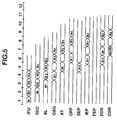
- the pipeline instructions shown in Fig. 4 are executed in a manner shown in Fig. 5. Namely, each instruction is fetched and processed for every clock; Instruction a2 having a memory operand is processed in the order from the instruction fetch section 2 ⁇ the decoder 3 ⁇ the instruction issue section 13 ⁇ the operand address section 4 ⁇ the address translation section 5 ⁇ the operand fetch section 6 to the second operation execution section 11.
- Instruction a2 having no memory operand but only a register operand is processed in the order from the instruction fetch section 2 ⁇ the decoder 3 ⁇ the instruction issue section 13 to the first operation execution section 10.
- the general purpose register group 8′ comprises register group for holding resulting data program-processed which will be described later and register group for temporarily holding the execution result of instruction in the look-forward manner, i.e., the two register groups are duplicated.
- the first operation execution section 10 comprises a first operator 20 and a first instruction register 21
- the second operation execution section 11 comprises a second operator 22 and a second instruction register 23
- the third operation execution section 12 comprises a third operator 24 and a third instruction register 25.
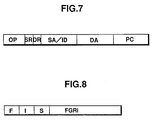
- Each of the instruction registers 21, 23, and 25 has an instruction format shown in Fig. 7.
- OP indicates an operational function designation field of the associated operators
- SR indicates a source register designation field
- DR a destination register field
- SA/ID a source operand address or immediate data holding field
- DA a destination operand address holding field
- PC an address holding field of an instruction in execution.
- reference numeral 30 indicates an instruction address compare section, which is included in the general purpose register 8′.
- FIG. 8 there is shown a detailed format of the register group FGR which is consisted of three tag portions F, I, S each consisting of three bits and a data holding portion FGRi for holding each data.
- each PC field of the instruction registers 21, 23, 25 is applied to the instruction address compare section 30 in order to determine whether or not a succeeding instruction is being executed by jumping a preceding instruction, for the comparisons of each PC field.
- the PC field of the first instruction register 21 shown in Fig. 3 contains the address of the instruction a2 at the fifth clock at which time the instruction a2 is to be executed and the PC field of the second instruction register 23 contains the instruction a1.
- the PC field of the third instruction register 25 contains no address. As a result, no instruction is executed in the third operation execution section 12.
- the data necessary for the calculation of the effective address of the next instruction a3 can be picked up from the FGR2 (which corresponds to the register R2) at the termination of the fifth clock. As a result, the instruction a3 can be moved to the effective address calculation section 4 immediately.
- the operation execution section is duplicated so as to execute a plurality of instructions simultaneously, while the general purpose register group is also divided into a second register group for storing data processed along the program flow and a first register group for storing data as a result of having in look-forward manner executed a succeeding instruction.
- a compare and decision means whereby a decision is made whether or not the succeeding instruction is being executed by jumping the preceding instructions and the processed data which have been held in the first register group are sent to the second register group so as to replace them in the form along the program flow in accordance with the result of the decision.
Description
- The present invention relates to an instruction parallel execution type microprocessor, more particularly to an instruction pipeline type microprocessor capable of rapidly executing instructions.
- In the instruction pipeline type microprocessor according to the prior art, a particular register or registers are used in order to perform an operand address calculation in such as an ADD instruction. However, as the content of the register is modified by a previous instruction such as a TRANSFER instruction, the ADD instruction can not be shifted to an operand address calculation stage before a write stage to a general purpose register is terminated, thus delaying the processing of the instruction.
- Namely, Fig. 2 shows an outline construction of the instruction pipeline type microporcessor according to the prior art.
- In Fig. 2,
reference numeral 1 indicates a bus control section (BCU) for connecting a microprocessor P to an external circuit,numeral 2 indicates an instruction fetch section (IFU), 3 indicates a decoder (DEC) for decoding instructions, 4 an operand address calculation section (OAG), 5 an address translation section (AT) for converting a logical address into a physical address, 6 an operand fetch section (OPF) for fetching an operand, 7 an operation execution section (EXU) for executing instructions, 8 general purpose register group (GR) consisting of a plurality of registers R₁, R₂, R₃, R₄, ... (not indicated). - When machine instructions shown in Fig. 1 are executed by the microprocessor P shown in Fig. 2 for instance, the timing of the instruction pipeline processing becomes the one shown in Fig. 3. As shown in Figs. 1 and 3, supposing that a₁ is an instruction which transfers the content of an address A to the register R₁ (not indicated) in GR₈, a₂ is an instruction which transfers data in the register R₃ in GR₈ to the register R₂, a₃ is an ADD instruction which transfers the content of an address B which is modified by the register R₂ to the register R₄, and a₄ is an instruction which transfers data in the register R₂ to a memory indicated by address C, the content of the register R₂ is used by the instruction a₃ in order to perform an operand address calculation. However, the content of the register R₂ is modified by the instruction a₂. As a result, the instruction a₃ can not move to OAG₄ until the transfer of the instruction a₂ to GR₈ is terminated, thus delaying the processing of the instruction a₃.
- Since the operation execution section and the general purpose register group in the microprocessor according to the prior art are not duplicated, succeeding instructions can not be executed only after the instructions for updating the general purpose register group GR₈ have been completely executed.
- Accordingly, the merits of the pipeline system can not be demonstrated due to stagnation of the processing flow in the instruction pipeline type microprocessors according to this prior art.
- The article "Design considerations for 32 bit microprocessor TX3" by K. OKAMOTO ET AL., in SPRING COMPCON 88, March 4, 1988, SAN FRANCISCO, CA, US, pages 25-29, describes an instruction pipeline type microprocessor comprising a plurality of simultaneously operating operation execution sections.
- Each decoded instruction is issued in order of program sequence, but instructions may complete out of order because of differences in execution time or number of pipeline stages. In order to ensure precise interrupts and traps, TX3 has a Reorder Buffer and two general register files which are the Current GR file and the Future GR file. (Precise interrupts and traps require that all instructions prior to the interrupted instruction have completed and all instructions following the interrupted instruction have not begun.) The Future GR file maintains the copies of the registers used for normal program execution, and the Current GR file holds the state of the registers to be used in case of an interrupt or trap. The Reorder Buffer keeps track of which instructions have been issued, and in what order. Register writes are sent immediately to the Future GR file, but are queued by the Reorder buffer to be written to the Current GR file as the immediately previous instruction completes. (Additional logic ensures that results are computed before they are read.)
-
- It is therefore an object of the present invention to provide an instruction pipeline type microprocessor comprising a plurality of simultaneously operating operation execution sections having a simpler circuitry for reordering.
- According to the present invention there is provided an instruction pipeline type microprocessor as claimed in
Claim 1. - These and other objects, features and advantages of the present invention will be more apparent from the following description of a preferred embodiment, taken in conjunction with the accompanying drawings.
-
- Fig. 1 is one example of a program for clarifying problems which the microprocessors according to the prior art have,
- Fig. 2 is the construction of the microprocessor of the instruction pipeline type according to the prior art,
- Fig. 3 illustrates a flow of instruction processing in the microprocessor shown in Fig. 2,
- Fig. 4 is a basic construction of the instruction pipeline type microprocessor according to the present invention,
- Fig. 5 illustrates a flow of instruction processing in each section constituting the microprocessor shown in Fig. 4,
- Fig. 6 is a detailed construction of the operation execution section and the general purpose register group shown in Fig. 4,
- Fig. 7 illustrates a format of each instruction register shown in Fig. 6, and
- Fig. 8 illustrates an input format of the register group FGR for storing the result of the instructions in the general purpose registers, processed in a look-forward manner.
-
- Fig. 4 shows a principle construction of the instruction pipeline type microprocessor according to the present invention.
- In the figure, same constructing elements as those shown in Fig. 2 are indicated by the same reference numerals. The instruction pipeline type microprocessor comprises an operation execution section consisting of a first operation execution (SEP) 10 for executing instructions having no memory operand respectively, a second operation execution section (IEP) 11 for executing instructions having memory operand respectively, and a third operation execution section (FEP) 12 for executing floating point instructions. In addition,
reference numeral 13 indicates an instruction sending section for sending decoded instructions to each operation section andnumeral 14 indicates a floating point register. - In the microprocessor according to the present invention shown in Fig. 4, the pipeline instructions shown in Fig. 4 are executed in a manner shown in Fig. 5. Namely, each instruction is fetched and processed for every clock; Instruction a₂ having a memory operand is processed in the order from the
instruction fetch section 2 → thedecoder 3 → theinstruction issue section 13 → theoperand address section 4 → theaddress translation section 5 → theoperand fetch section 6 to the secondoperation execution section 11. - Instruction a₂ having no memory operand but only a register operand is processed in the order from the
instruction fetch section 2 → thedecoder 3 → theinstruction issue section 13 to the firstoperation execution section 10. - As shown in Fig. 5, since the executions of the instructions a₂ and a₁ are terminated at the fifth and sixth clocks respectively, it is necessary to avoid discrepancy between the data in the general
purpose register group 8′ and the program flow. To this end, the generalpurpose register group 8′ comprises register group for holding resulting data program-processed which will be described later and register group for temporarily holding the execution result of instruction in the look-forward manner, i.e., the two register groups are duplicated. - In Fig. 6, the first
operation execution section 10 comprises afirst operator 20 and afirst instruction register 21, the secondoperation execution section 11 comprises asecond operator 22 and asecond instruction register 23, and the thirdoperation execution section 12 comprises athird operator 24 and athird instruction register 25. Each of the instruction registers 21, 23, and 25 has an instruction format shown in Fig. 7. - That is to say, in Fig. 7, OP indicates an operational function designation field of the associated operators, SR indicates a source register designation field, DR a destination register field, SA/ID a source operand address or immediate data holding field, DA a destination operand address holding field, and PC an address holding field of an instruction in execution.
- Returning to Fig. 6, the general
purpose register group 8′ is divided into a register group CGRi (i= 1,2, 3, ... n) for storing data as a result processed in accordance with a program and a register group FGRi (i = 1, 2, 3, ... n). Moreover, in Fig. 6,reference numeral 30 indicates an instruction address compare section, which is included in thegeneral purpose register 8′. - In Fig. 8, there is shown a detailed format of the register group FGR which is consisted of three tag portions F, I, S each consisting of three bits and a data holding portion FGRi for holding each data.
- Now, turning back to Fig. 6, each PC field of the
instruction registers section 30 in order to determine whether or not a succeeding instruction is being executed by jumping a preceding instruction, for the comparisons of each PC field. - From the result of the comparison, when the PC field of the
first instruction register 21 is not minimum "1" output signal is produced from the output C₁ of the compare section and when the PC field of thesecond instruction register 23 is not minimum, "1" output signal is produced from the output C₂ thereof, while when the DC field of theinstruction register 25 is not minimum, "1" output signal is produced from the output C₃ thereof. - Furthermore, when the address PC of the instruction register in the operator which has executed an instruction is not minimum, "1" output signal (FGR WRITE signal) is produced from the output C₄ of the address compare
section 30, while when the address PC of the instruction register is minimum, "1" output signal (CGR WRITE signal) is produced from the output C₅ of thecompare section 30. - When the operation in each operator is terminated, the tag S in the register FGR is set at "1" when C₄=1, C₁=1, and the I tag is set at "1" when C₂=1, while the F tag is set at "1" when C₃=1.
- The operation result from each of the
operators instruction registers - When the operation of each of the
operators - Accordingly, as shown in Fig. 5, in operation, the PC field of the
first instruction register 21 shown in Fig. 3, contains the address of the instruction a₂ at the fifth clock at which time the instruction a₂ is to be executed and the PC field of thesecond instruction register 23 contains the instruction a₁. However, since an instruction has not been sent to the PC field of thethird instruction register 25 from theinstruction sending section 13, its PC field contains no address. As a result, no instruction is executed in the thirdoperation execution section 12. - On the other hand, since the
first instruction register 21 contains the instruction a₂ and the address PC field thereof is larger than that of the instruction a₁, C₁=1 is established and the result of the operation is written into FGR₂ while the tag S is set at "1". - The instruction a₁ is executed in the
second operator 11 in the sixth clock. In this case, however, as theinstruction register 21 in thefirst operator 10 contains no instruction because the instruction a₂ has already been executed therein, no action is performed. Accordingly, since C₄=0, C₅=1, the result of the operation of the instruction a₁ is stored in the CGR₁ and FGR₁, while the data in FGR₂ in which the tag S₁ has been set at "1" is now transferred to CGR₂ and is stored for a later use as data processed along the program flow. - As will be appreciated from the above description, the data necessary for the calculation of the effective address of the next instruction a₃ can be picked up from the FGR₂ (which corresponds to the register R₂) at the termination of the fifth clock. As a result, the instruction a₃ can be moved to the effective
address calculation section 4 immediately. - Accordingly, unlike the microprocessors of this type according to the prior art, in the instruction pipeline type microprocessor according to the present invention, a sequential program processing in such that the instruction a₃ is processed only after the instructions a₁ and a₂ have been executed, is not required in the present invention.
- As has been described in the foregoing, in the instruction pipeline type microprocessor according to the present invention, the operation execution section is duplicated so as to execute a plurality of instructions simultaneously, while the general purpose register group is also divided into a second register group for storing data processed along the program flow and a first register group for storing data as a result of having in look-forward manner executed a succeeding instruction.
- In the instruction pipeline type microprocessor according to the present invention, there is also provided a compare and decision means whereby a decision is made whether or not the succeeding instruction is being executed by jumping the preceding instructions and the processed data which have been held in the first register group are sent to the second register group so as to replace them in the form along the program flow in accordance with the result of the decision.
- Since succeeding instructions can be in look-forward manner executed without waiting for the result of the execution of the preceding instructions, the performance of the microprocessor of the instruction pipeline type according to the present invention can be strikingly improved.
Claims (3)
- An instruction pipeline type microprocessor, comprising:(a) means (2, 3, 13) for fetching, decoding and determining a plurality of different kinds of decoded instructions and sending the plurality of different kinds of decoded instructions in accordance with the determined different kinds;(b) a plurality of operation execution sections (10, 11, 12) for receiving the decoded instructions according to the determined different kinds and respectively executing the plurality of different kinds of decoded instructions simultaneously, wherein each of the plurality operation execution sections includes an instruction register (21: 23: 25) having at least an instruction address holding field (PC) indicative of the address of an instruction decoded in a program and a destination register designation field (DR) designating the location in a data holding section where the operation execution result has to be stored; said data holding system comprising(c) first storing means (FGRi) for storing the operation execution results in the order as being processed, wherein the first storing means includes a plurality of tag bits (F ; I ; S), one tag bit for each operation execution section (10, 11, 12), for indicating whether or not the corresponding operation execution section has executed an instruction (a₂) before a preceeding instruction (a₁) has been executed;(d) second storing means (CGRi) for storing the operation execution results in accordance with the program order;(e) compare means (30) for comparing the instruction address holding fields (PC) from the operation execution sections (10, 11, 12) and producing signals (C₁ ; C₂ ; ... ; C₅) indicative of the result of comparison, for sending the operation execution result and the corresponding tag bit (F ; I ; S) to the first storing means (FGRi), based on the sequence of completion of the data processing, whereby the value of the corresponding tag bit (F ; I ; S) is determined by corresponding signals (C₁ ; C₂ ; C₃) from the comparator, or for sending the processed data to the first and second storing means, so that the processed data already stored in the first storing means (FGRi) are transferred to the second storing means (CGRi) in the predetermined program order according to compare results and contents of the tag bits (F ; I ; S).
- A microprocessor as claimed in claim 1, wherein said plurality of operation execution sections include a first operation execution section (10) for executing instructions having no memory operand respectively, a second operation execution section (11) for executing instructions having a memory operand respectively, and a third operation execution section (12) for executing floating point instructions.
- A microprocessor as claimed in claim 1 or 2, wherein said first storing means is comprised of a first register group (FRGi) for successively storing the result of the operations about instructions executed, and said second storing means comprised of a second register group (CGRi) for storing the results of the operations along the predetermined program flow.
Applications Claiming Priority (2)
| Application Number | Priority Date | Filing Date | Title |
|---|---|---|---|
| JP63198789A JPH0673105B2 (en) | 1988-08-11 | 1988-08-11 | Instruction pipeline type microprocessor |
| JP198789/88 | 1988-08-11 |
Publications (3)
| Publication Number | Publication Date |
|---|---|
| EP0354585A2 EP0354585A2 (en) | 1990-02-14 |
| EP0354585A3 EP0354585A3 (en) | 1991-11-13 |
| EP0354585B1 true EP0354585B1 (en) | 1995-11-22 |
Family
ID=16396934
Family Applications (1)
| Application Number | Title | Priority Date | Filing Date |
|---|---|---|---|
| EP89114907A Expired - Lifetime EP0354585B1 (en) | 1988-08-11 | 1989-08-11 | Instruction pipeline microprocessor |
Country Status (4)
| Country | Link |
|---|---|
| EP (1) | EP0354585B1 (en) |
| JP (1) | JPH0673105B2 (en) |
| KR (1) | KR920004290B1 (en) |
| DE (1) | DE68924883T2 (en) |
Cited By (7)
| Publication number | Priority date | Publication date | Assignee | Title |
|---|---|---|---|---|
| US6434693B1 (en) | 1992-09-29 | 2002-08-13 | Seiko Epson Corporation | System and method for handling load and/or store operations in a superscalar microprocessor |
| US6735685B1 (en) | 1992-09-29 | 2004-05-11 | Seiko Epson Corporation | System and method for handling load and/or store operations in a superscalar microprocessor |
| US7685402B2 (en) | 1991-07-08 | 2010-03-23 | Sanjiv Garg | RISC microprocessor architecture implementing multiple typed register sets |
| US7721070B2 (en) | 1991-07-08 | 2010-05-18 | Le Trong Nguyen | High-performance, superscalar-based computer system with out-of-order instruction execution |
| US7802074B2 (en) | 1992-03-31 | 2010-09-21 | Sanjiv Garg | Superscalar RISC instruction scheduling |
| US7934078B2 (en) | 1992-05-01 | 2011-04-26 | Seiko Epson Corporation | System and method for retiring approximately simultaneously a group of instructions in a superscalar microprocessor |
| US8074052B2 (en) | 1992-12-31 | 2011-12-06 | Seiko Epson Corporation | System and method for assigning tags to control instruction processing in a superscalar processor |
Families Citing this family (7)
| Publication number | Priority date | Publication date | Assignee | Title |
|---|---|---|---|---|
| JPH04111127A (en) * | 1990-08-31 | 1992-04-13 | Toshiba Corp | Arithmetic processor |
| EP0547247B1 (en) | 1991-07-08 | 2001-04-04 | Seiko Epson Corporation | Extensible risc microprocessor architecture |
| EP0945787A3 (en) * | 1991-07-08 | 2008-12-31 | Seiko Epson Corporation | Risc microprocessor architecture implementing fast trap and exception state |
| US5961629A (en) * | 1991-07-08 | 1999-10-05 | Seiko Epson Corporation | High performance, superscalar-based computer system with out-of-order instruction execution |
| US5438668A (en) | 1992-03-31 | 1995-08-01 | Seiko Epson Corporation | System and method for extraction, alignment and decoding of CISC instructions into a nano-instruction bucket for execution by a RISC computer |
| US5371684A (en) | 1992-03-31 | 1994-12-06 | Seiko Epson Corporation | Semiconductor floor plan for a register renaming circuit |
| US5850563A (en) * | 1995-09-11 | 1998-12-15 | International Business Machines Corporation | Processor and method for out-of-order completion of floating-point operations during load/store multiple operations |
Family Cites Families (7)
| Publication number | Priority date | Publication date | Assignee | Title |
|---|---|---|---|---|
| JPS5110746A (en) * | 1974-07-17 | 1976-01-28 | Hitachi Ltd | |
| JPS5729153A (en) * | 1980-07-29 | 1982-02-17 | Fujitsu Ltd | Control system for instruction processing order |
| JPS57161938A (en) * | 1981-03-30 | 1982-10-05 | Fujitsu Ltd | Instruction control system |
| JPS581246A (en) * | 1981-06-26 | 1983-01-06 | Fujitsu Ltd | Controlling system for order of instruction processing |
| US4594660A (en) * | 1982-10-13 | 1986-06-10 | Honeywell Information Systems Inc. | Collector |
| JPS60126734A (en) * | 1983-12-13 | 1985-07-06 | Nec Corp | Information processing device |
| JPS6116335A (en) * | 1984-07-02 | 1986-01-24 | Nec Corp | Information processor |
-
1988
- 1988-08-11 JP JP63198789A patent/JPH0673105B2/en not_active Expired - Fee Related
-
1989
- 1989-08-05 KR KR1019890011190A patent/KR920004290B1/en not_active IP Right Cessation
- 1989-08-11 DE DE68924883T patent/DE68924883T2/en not_active Expired - Fee Related
- 1989-08-11 EP EP89114907A patent/EP0354585B1/en not_active Expired - Lifetime
Cited By (10)
| Publication number | Priority date | Publication date | Assignee | Title |
|---|---|---|---|---|
| US7685402B2 (en) | 1991-07-08 | 2010-03-23 | Sanjiv Garg | RISC microprocessor architecture implementing multiple typed register sets |
| US7721070B2 (en) | 1991-07-08 | 2010-05-18 | Le Trong Nguyen | High-performance, superscalar-based computer system with out-of-order instruction execution |
| US7802074B2 (en) | 1992-03-31 | 2010-09-21 | Sanjiv Garg | Superscalar RISC instruction scheduling |
| US7934078B2 (en) | 1992-05-01 | 2011-04-26 | Seiko Epson Corporation | System and method for retiring approximately simultaneously a group of instructions in a superscalar microprocessor |
| US7958337B2 (en) | 1992-05-01 | 2011-06-07 | Seiko Epson Corporation | System and method for retiring approximately simultaneously a group of instructions in a superscalar microprocessor |
| US6434693B1 (en) | 1992-09-29 | 2002-08-13 | Seiko Epson Corporation | System and method for handling load and/or store operations in a superscalar microprocessor |
| US6735685B1 (en) | 1992-09-29 | 2004-05-11 | Seiko Epson Corporation | System and method for handling load and/or store operations in a superscalar microprocessor |
| US7844797B2 (en) | 1992-09-29 | 2010-11-30 | Seiko Epson Corporation | System and method for handling load and/or store operations in a superscalar microprocessor |
| US8019975B2 (en) | 1992-09-29 | 2011-09-13 | Seiko-Epson Corporation | System and method for handling load and/or store operations in a superscalar microprocessor |
| US8074052B2 (en) | 1992-12-31 | 2011-12-06 | Seiko Epson Corporation | System and method for assigning tags to control instruction processing in a superscalar processor |
Also Published As
| Publication number | Publication date |
|---|---|
| JPH0673105B2 (en) | 1994-09-14 |
| JPH0248732A (en) | 1990-02-19 |
| EP0354585A3 (en) | 1991-11-13 |
| EP0354585A2 (en) | 1990-02-14 |
| KR900003743A (en) | 1990-03-27 |
| DE68924883T2 (en) | 1996-05-15 |
| KR920004290B1 (en) | 1992-06-01 |
| DE68924883D1 (en) | 1996-01-04 |
Similar Documents
| Publication | Publication Date | Title |
|---|---|---|
| EP0405489B1 (en) | Resource conflict detection method and apparatus included in a pipelined processing unit | |
| US6247106B1 (en) | Processor configured to map logical register numbers to physical register numbers using virtual register numbers | |
| JP3637920B2 (en) | System and method for retirement of instructions in a superscaler microprocessor | |
| EP0437044B1 (en) | Data processing system with instruction tag apparatus | |
| US5150468A (en) | State controlled instruction logic management apparatus included in a pipelined processing unit | |
| EP0354585B1 (en) | Instruction pipeline microprocessor | |
| JPH07160501A (en) | Data processing system | |
| US5023828A (en) | Microinstruction addressing in high-speed CPU | |
| JP2620511B2 (en) | Data processor | |
| US5832202A (en) | Exception recovery in a data processing system | |
| EP0094535B1 (en) | Pipe-line data processing system | |
| EP0378415A2 (en) | Multiple instruction dispatch mechanism | |
| US6230262B1 (en) | Processor configured to selectively free physical registers upon retirement of instructions | |
| US20020112142A1 (en) | Implementation of a conditional move instruction in an out-of-order processor | |
| US5291615A (en) | Instruction pipeline microprocessor | |
| EP0240606A2 (en) | Pipe-line processing system and microprocessor using the system | |
| JPH0419575B2 (en) | ||
| JPS6065343A (en) | Instruction processor | |
| KR19980028841A (en) | Index first-in, first-out circuit with lockbits for checking data dependencies in register files |
Legal Events
| Date | Code | Title | Description |
|---|---|---|---|
| PUAI | Public reference made under article 153(3) epc to a published international application that has entered the european phase |
Free format text: ORIGINAL CODE: 0009012 |
|
| 17P | Request for examination filed |
Effective date: 19890811 |
|
| AK | Designated contracting states |
Kind code of ref document: A2 Designated state(s): DE FR GB |
|
| PUAL | Search report despatched |
Free format text: ORIGINAL CODE: 0009013 |
|
| AK | Designated contracting states |
Kind code of ref document: A3 Designated state(s): DE FR GB |
|
| 17Q | First examination report despatched |
Effective date: 19931215 |
|
| GRAA | (expected) grant |
Free format text: ORIGINAL CODE: 0009210 |
|
| AK | Designated contracting states |
Kind code of ref document: B1 Designated state(s): DE FR GB |
|
| ET | Fr: translation filed | ||
| REF | Corresponds to: |
Ref document number: 68924883 Country of ref document: DE Date of ref document: 19960104 |
|
| PLBE | No opposition filed within time limit |
Free format text: ORIGINAL CODE: 0009261 |
|
| STAA | Information on the status of an ep patent application or granted ep patent |
Free format text: STATUS: NO OPPOSITION FILED WITHIN TIME LIMIT |
|
| 26N | No opposition filed | ||
| REG | Reference to a national code |
Ref country code: GB Ref legal event code: 746 Effective date: 19981026 |
|
| REG | Reference to a national code |
Ref country code: FR Ref legal event code: D6 |
|
| REG | Reference to a national code |
Ref country code: GB Ref legal event code: IF02 |
|
| PGFP | Annual fee paid to national office [announced via postgrant information from national office to epo] |
Ref country code: DE Payment date: 20050804 Year of fee payment: 17 |
|
| PGFP | Annual fee paid to national office [announced via postgrant information from national office to epo] |
Ref country code: FR Payment date: 20050809 Year of fee payment: 17 |
|
| PGFP | Annual fee paid to national office [announced via postgrant information from national office to epo] |
Ref country code: GB Payment date: 20050810 Year of fee payment: 17 |
|
| PG25 | Lapsed in a contracting state [announced via postgrant information from national office to epo] |
Ref country code: DE Free format text: LAPSE BECAUSE OF NON-PAYMENT OF DUE FEES Effective date: 20070301 |
|
| GBPC | Gb: european patent ceased through non-payment of renewal fee |
Effective date: 20060811 |
|
| REG | Reference to a national code |
Ref country code: FR Ref legal event code: ST Effective date: 20070430 |
|
| PG25 | Lapsed in a contracting state [announced via postgrant information from national office to epo] |
Ref country code: GB Free format text: LAPSE BECAUSE OF NON-PAYMENT OF DUE FEES Effective date: 20060811 |
|
| PG25 | Lapsed in a contracting state [announced via postgrant information from national office to epo] |
Ref country code: FR Free format text: LAPSE BECAUSE OF NON-PAYMENT OF DUE FEES Effective date: 20060831 |