EP0373565A2 - Method of driving a display unit - Google Patents
Method of driving a display unit Download PDFInfo
- Publication number
- EP0373565A2 EP0373565A2 EP89122847A EP89122847A EP0373565A2 EP 0373565 A2 EP0373565 A2 EP 0373565A2 EP 89122847 A EP89122847 A EP 89122847A EP 89122847 A EP89122847 A EP 89122847A EP 0373565 A2 EP0373565 A2 EP 0373565A2
- Authority
- EP
- European Patent Office
- Prior art keywords
- display unit
- voltage
- potential
- driving
- line
- Prior art date
- Legal status (The legal status is an assumption and is not a legal conclusion. Google has not performed a legal analysis and makes no representation as to the accuracy of the status listed.)
- Granted
Links
Images


Classifications
-
- G—PHYSICS
- G09—EDUCATION; CRYPTOGRAPHY; DISPLAY; ADVERTISING; SEALS
- G09G—ARRANGEMENTS OR CIRCUITS FOR CONTROL OF INDICATING DEVICES USING STATIC MEANS TO PRESENT VARIABLE INFORMATION
- G09G3/00—Control arrangements or circuits, of interest only in connection with visual indicators other than cathode-ray tubes
- G09G3/20—Control arrangements or circuits, of interest only in connection with visual indicators other than cathode-ray tubes for presentation of an assembly of a number of characters, e.g. a page, by composing the assembly by combination of individual elements arranged in a matrix no fixed position being assigned to or needed to be assigned to the individual characters or partial characters
- G09G3/34—Control arrangements or circuits, of interest only in connection with visual indicators other than cathode-ray tubes for presentation of an assembly of a number of characters, e.g. a page, by composing the assembly by combination of individual elements arranged in a matrix no fixed position being assigned to or needed to be assigned to the individual characters or partial characters by control of light from an independent source
- G09G3/36—Control arrangements or circuits, of interest only in connection with visual indicators other than cathode-ray tubes for presentation of an assembly of a number of characters, e.g. a page, by composing the assembly by combination of individual elements arranged in a matrix no fixed position being assigned to or needed to be assigned to the individual characters or partial characters by control of light from an independent source using liquid crystals
- G09G3/3611—Control of matrices with row and column drivers
- G09G3/3648—Control of matrices with row and column drivers using an active matrix
- G09G3/3655—Details of drivers for counter electrodes, e.g. common electrodes for pixel capacitors or supplementary storage capacitors
-
- G—PHYSICS
- G09—EDUCATION; CRYPTOGRAPHY; DISPLAY; ADVERTISING; SEALS
- G09G—ARRANGEMENTS OR CIRCUITS FOR CONTROL OF INDICATING DEVICES USING STATIC MEANS TO PRESENT VARIABLE INFORMATION
- G09G3/00—Control arrangements or circuits, of interest only in connection with visual indicators other than cathode-ray tubes
- G09G3/20—Control arrangements or circuits, of interest only in connection with visual indicators other than cathode-ray tubes for presentation of an assembly of a number of characters, e.g. a page, by composing the assembly by combination of individual elements arranged in a matrix no fixed position being assigned to or needed to be assigned to the individual characters or partial characters
- G09G3/34—Control arrangements or circuits, of interest only in connection with visual indicators other than cathode-ray tubes for presentation of an assembly of a number of characters, e.g. a page, by composing the assembly by combination of individual elements arranged in a matrix no fixed position being assigned to or needed to be assigned to the individual characters or partial characters by control of light from an independent source
- G09G3/36—Control arrangements or circuits, of interest only in connection with visual indicators other than cathode-ray tubes for presentation of an assembly of a number of characters, e.g. a page, by composing the assembly by combination of individual elements arranged in a matrix no fixed position being assigned to or needed to be assigned to the individual characters or partial characters by control of light from an independent source using liquid crystals
- G09G3/3611—Control of matrices with row and column drivers
- G09G3/3648—Control of matrices with row and column drivers using an active matrix
- G09G3/3659—Control of matrices with row and column drivers using an active matrix the addressing of the pixel involving the control of two or more scan electrodes or two or more data electrodes, e.g. pixel voltage dependant on signal of two data electrodes
-
- G—PHYSICS
- G09—EDUCATION; CRYPTOGRAPHY; DISPLAY; ADVERTISING; SEALS
- G09G—ARRANGEMENTS OR CIRCUITS FOR CONTROL OF INDICATING DEVICES USING STATIC MEANS TO PRESENT VARIABLE INFORMATION
- G09G2300/00—Aspects of the constitution of display devices
- G09G2300/08—Active matrix structure, i.e. with use of active elements, inclusive of non-linear two terminal elements, in the pixels together with light emitting or modulating elements
- G09G2300/0876—Supplementary capacities in pixels having special driving circuits and electrodes instead of being connected to common electrode or ground; Use of additional capacitively coupled compensation electrodes
-
- G—PHYSICS
- G09—EDUCATION; CRYPTOGRAPHY; DISPLAY; ADVERTISING; SEALS
- G09G—ARRANGEMENTS OR CIRCUITS FOR CONTROL OF INDICATING DEVICES USING STATIC MEANS TO PRESENT VARIABLE INFORMATION
- G09G2310/00—Command of the display device
- G09G2310/06—Details of flat display driving waveforms
-
- G—PHYSICS
- G09—EDUCATION; CRYPTOGRAPHY; DISPLAY; ADVERTISING; SEALS
- G09G—ARRANGEMENTS OR CIRCUITS FOR CONTROL OF INDICATING DEVICES USING STATIC MEANS TO PRESENT VARIABLE INFORMATION
- G09G2320/00—Control of display operating conditions
- G09G2320/02—Improving the quality of display appearance
- G09G2320/0204—Compensation of DC component across the pixels in flat panels
-
- G—PHYSICS
- G09—EDUCATION; CRYPTOGRAPHY; DISPLAY; ADVERTISING; SEALS
- G09G—ARRANGEMENTS OR CIRCUITS FOR CONTROL OF INDICATING DEVICES USING STATIC MEANS TO PRESENT VARIABLE INFORMATION
- G09G2320/00—Control of display operating conditions
- G09G2320/02—Improving the quality of display appearance
- G09G2320/0219—Reducing feedthrough effects in active matrix panels, i.e. voltage changes on the scan electrode influencing the pixel voltage due to capacitive coupling
-
- G—PHYSICS
- G09—EDUCATION; CRYPTOGRAPHY; DISPLAY; ADVERTISING; SEALS
- G09G—ARRANGEMENTS OR CIRCUITS FOR CONTROL OF INDICATING DEVICES USING STATIC MEANS TO PRESENT VARIABLE INFORMATION
- G09G2320/00—Control of display operating conditions
- G09G2320/02—Improving the quality of display appearance
- G09G2320/0247—Flicker reduction other than flicker reduction circuits used for single beam cathode-ray tubes
-
- G—PHYSICS
- G09—EDUCATION; CRYPTOGRAPHY; DISPLAY; ADVERTISING; SEALS
- G09G—ARRANGEMENTS OR CIRCUITS FOR CONTROL OF INDICATING DEVICES USING STATIC MEANS TO PRESENT VARIABLE INFORMATION
- G09G2320/00—Control of display operating conditions
- G09G2320/02—Improving the quality of display appearance
- G09G2320/0257—Reduction of after-image effects
Definitions
- the present invention relates to a method of AC driving a display unit made of display material such as liquid crystal by using an active matrix constructed of switching elements such as thin film transistors (hereinafter called TFT) and pixel electrodes, and also to a method of setting its drive voltages, respectively aiming at a) reduction of drive power, b) improvement on display quality, and c) improvement on drive reliability.
- TFT thin film transistors
- the first document “JAPAN DISPLAY” by T. Yanagisawa, et al, '86, p. 192 intends to compensate for the DC voltage by using an image signal voltage (Vsig) having different positive and negative amplitudes relative to a base or center voltage (Vc).
- the second document “Euro Display” by K. Suzuki, '87, p. 107 intends to compensate for the DC voltage by adding a negative signal (Ve) after a scan signal.
- the third problem is that a DC potential difference occurs between the average potential at an image signal line and that at a pixel electrode because a scan signal adversely effects the pixel electrode potential via a parasitic capacitor Cgd between the gate and drain of a TFT. If the potentials at various circuit portions of a display unit are set so as to make zero the average DC potential difference between the pixel electrodes and opposing electrode during the AC drive of liquid crystal, there is unavoidably generated the DC potential difference between the image signal line and opposing electrode. This DC potential difference results in a serious defect such as the image memory phenomenon. There is not known, however, a method of compensating for such DC potential difference.
- this capacitor coupled potential is supplied as a fraction of the liquid crystal drive voltage so that the amplitude of an image signal to be supplied from the image signal driver can be reduced correspondingly to reduce the drive power.
- a scan signal Vg is applied to the scan signal line 1, an image signal voltage Vsig to the image signal line 2, a modulating signal reversing its polarities Ve(+) and Ve(-) alternately for each field to one electrode of the storage capacitor Cs, and a voltage constant for all fields to the opposing electrode of the liquid crystal capacitor Clc*.
- the influence of the drive voltages is reflected upon the pixel electrode (at point A in Fig. 1) through electrostatic induction via the above-described parasitic capacitors and intentionally provided capacitors.
- conditional equations (3) and (4) include two voltage parameters Ve(+) and Ve(-) which can be arbitrarily set on the side of the display unit.
- the value of the potential change ⁇ V* at the pixel electrode can be arbitrarily set. If the value ⁇ V* is set larger than or equal to the threshold voltage of the liquid crystal, the signal Vsig of a smaller amplitude can be used. With a smaller amplitude signal Vsig, the amplitude of signals outputted from the image signal drive circuit dealing with analog signals can be made small so that the power consumption of the drive circuit can be reduced in proportion to the square of the amplitude.
- Fig. 4 shows voltage waveforms aiming at improving the drive method shown in Fig. 2, wherein used is a voltage waveform indicated at (b) in Fig. 4 different from that in Fig. 2.
- the modulating signal Ve is applied as in the following.
- T T2′
- T4′ after the completion of scanning by the signal Vg (after TRT turns off)
- the modulating signal is changed in the negative direction by the amount Ve(+).
- the display unit of the first embodiment of this invention is shown in Fig. 5.
- Reference numeral 11 designates a scan signal drive circuit
- 12 an image signal drive circuit
- 13 a first modulating circuit
- 14 a second modulating circuit.
- 15a, 15b, ..., 15z designates scan signal lines, 16a, 16b, ..., 16z image signal lines, 17a, 17b, ..., 17z common electrodes of storage capacitors Cs, and 18a, 18b, ..., 18z opposing electrodes of liquid crystals.
- ⁇ V* and Vsig are essentially the same as that shown in Fig. 2. Namely, the polarities of the image signal and modulating signals are reversed alternately for each field.
- all the range from black to white could be driven bt a signal voltage with its amplitude only 3Vpp, while retaining a good display contrast with less flickers.
- the DC components among respective electrodes were almost zero with a good reliability of the liquid crystal for a long period.
- the brightness control of a display image was carried out by changing the amplitude of the modulating signal and hence of ⁇ V*.
- a voltage waveform of Ve shown in Fig. 7 is used which is different from that of the first embodiment.
- the voltage of Ve is different between the even and odd fields.
- the modulating signals Ve(N) and Ve(N+1) are changed two steps in the negative direction. Specifically, the Ve potential is changed during the on-period of TFT, and after TFT turns off, changed further in the negative direction by the amount smaller than the change in the positive direction.
- this embodiment has another advantage that since the change of Ve in the negative direction during the on-period of TFT is small, the gate voltage necessary for a given image signal voltage is reduced.
- the waveform of Vt at each scan line is reversed alternately for each field.
- the waveform of Vt changes its polarity during the on-period of TFT in the direction opposite to that the waveform Ve changes after the turning-off of TFT.
- the modulating voltages Ve(+) and Ve(-) become smaller than those of the first and second embodiments.
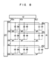
- FIG. 8 The circuit of the display unit of the fourth embodiment is shown in Fig. 8 and the voltage waveforms applied to this circuit are shown in Fig. 9.
- reference numeral 21a designates a first scan signal line, 21a′ a common electrode line of storage capacitors at the first scan signal line, 21z the last scan signal line, and 21z′ a scan signal line at the stage before the last stage.
- This embodiment is different from the first and second embodiments in that the common electrode of storage capacitors is connected to the scan line at the preceding stage.
- the modulating signal is therefore applied to the preceding stage scan signal line.
- a delay time ⁇ d lapses after scanning the (N+1)-th scan signal line, the polarity of the modulating signal applied to the N-th scan signal line is reversed.
- the display unit having the same circuit as the fourth embodiment is driven by the signals having the waveforms shown in Fig. 10.
- the voltage Vg after modulation is the same for both the even and odd fields, whereas in this embodiment it is different between the even and odd fields.
- the waveforms shown in Fig. 10 not only the advantages of the fourth embodiment are obtained, but also the gate amplitude required for driving the gate is made smaller.
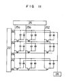
- the circuit of the display unit of the sixth embodiment is shown in Fig. 11, and the voltage waveforms applied to this circuit are shown in Fig. 12.
- This embodiment is the same as the fourth embodiment in that the modulating signal is applied to the scan signal line, but is different from the already described embodiments in that the opposing electrodes are not grouped into each scan signal line but all the electrodes within the display unit are supplied with a same potential, and in that the polarity of the potential between the pixel electrode and opposing electrode is changed alternately for each one scan period (1 H).
- reference numeral 22 designates a scan signal drive circuit, 25 an image signal drive circuit, and 26 a second modulation signal generating circuit.
- Reference numerals 25a, 25b, ..., 25z designate image signal lines.
- Ch(N) and Ch(N1) represent the voltage waveforms applied to the N-th and (N+1)-th scan signal lines, respectively.
- Vt represents the opposing electrode potential
- Vsig represents the image signal voltage waveform.
- the voltage waveforms for AC driving the liquid crystal have their polarities reversed alternately for the even and odd fields, as shown in Figs. 12A and 12B.
- the potentials Ve(+) and VE(-) of the modulating signal immediately after the scan signal Vg in the waveforms Ch(N) and Ch(N+1) are changed independently of each other.
- the duration Ts of the scan signal Vg is made variable within the period smaller than one scan period. After the lapse of a delay time ⁇ d after scanning the succeeding stage Ch(N+1) scan line, the modulating signal is applied.
- the number of second modulating signal output lines for the opposing electrodes can be reduced.
- the occurrence of the image memory phenomenon was checked by displaying a fixed pattern such as window pattern, color bar, and resolution chart on the display unit and by using the drive method of this embodiment. After displaying a window pattern for four hours, the whole screen of the display unit was set at the halftone display condition. The burning phenomenon of the fixed pattern was not observed.
- the image burning phenomenon of two display panels driven in accordance with the conventional method was also checked for comparison therebetween.
- the first display panel has no storage capacitor for each pixel. With this display panel, the internal DC potential difference between the image signal line and pixel electrode induced by the scan signal via the parasitic capacitor Cgd is 3.5 to 4.0 V. After displaying a window pattern on this display panel for three minutes, the burning phenomenon was clearly observed. Also, after displaying a window pattern on this display panel for one hour, the burning phenomenon did not disappear for three hours. Other fixed patterns also resulted in the same burning phenomenon.
- the second display panel has a storage capacitor of 1 pF for each pixel, and the internal DC potential difference is 0.7 to 1.0 V. After displaying a fixed pattern for several minutes on this display panel, the burning phenomenon was not observed definitely, but after the one hour consecutive display, it was observed and continued thereafter for several hours.
- the voltage waveforms of the fifth embodiment are used while the potential of the second modulating signal generator shown in Fig. 11 is made floated, i.e., while the opposing electrode are not connected to any circuit portion.
- the modulating signal Ve applied to the scan signal line is induced, via the internal electrostatic capacitor within the display unit, also to the opposing electrode.
- the image signal line is held at the potential irrelevant to the modulating signal Ve so that the amplitude of the second demodulating signal appearing at the opposing electrode is in general smaller than Ve, thereby not satisfying the conditional equation (4b′) correctly.
- the second modulating signal generator can be omitted, resulting in a large reduction of power consumption. An image of good quality can be displayed also in this case, satisfying almost all of the objects of the present invention.
- the storage capacitor common lines 17a, 17b, ..., 17z are connected together and the opposing electrode common lines 18a, 18b, ..., 18z are connected together in the first embodiment shown in Fig. 5, and the display panel is driven in an analogous way to sixth embodiment which changes the potential polarity of the pixel electrode alternately for each one scan period.
- the circuit shown in Fig. 11 is used and the voltage waveforms shown in Fig. 13 are applied to the display unit.
- the voltage waveforms Ch(N) and Ch(N+1) shown in Fig. 13 are modifications of those of the sixth embodiment shown in Fig. 12.
- the voltage waveform Ch(N) in the odd field shown in Fig. 13A takes a potential Ve(+) after the on-period Ts of TFT, and after the lapse of a delay time ⁇ d′ (0 ⁇ ⁇ d′ ⁇ Ts) after turning-on of TFT at the succeeding scan line as shown by Ch(N+1), takes a potential Ve(-).
- This embodiment uses the circuit shown in Fig. 11 and the applied voltage waveforms shown in Fig. 14 which shows another modification of the voltage waveforms Ch(N) and Ch(N+1) of the sixth embodiment shown in Fig. 12.
- the voltage waveform Ch(N) in the odd field shown in Fig. 14A takes a zero potential after the on-period Ts of TFT, and after the lapse of a delay time ⁇ d′ (0 ⁇ ⁇ d′ ⁇ Ts) after turning-on of TFT at the succeeding scan line as shown by Ch(N+1), takes a potential Ve(-).
- the voltage waveform Ch(N+1) in the even field takes a zero potential after the on-period of TFT, and after the lapse of a delay time ⁇ d′ (0 ⁇ ⁇ d′ ⁇ Ts) after turning-on of TFT at the succeeding scan line as shown by Ch(N+1), takes a potential Ve(+).
- Ch(N) in the odd field and Ch(N+1) in the even field are the same voltage waveform, and Ch(N) in the even field and Ch(N+1) in the odd field are the same voltage waveform.
- the present invention has the following distinctive advantages.
- the amplitude of voltage signals to be generated from the signal drive circuits in an active matrix display unit is considerably lowered, resulting in a reduction of power consumption by the drive circuits which deal with analog signals. Further, in the case of a color display, the amplitude of signals of chroma ICs are lowered to thus reduce power consumption. The drive power for the display unit as a whole can thus be reduced.
- the lower amplitude of voltage signals makes it easy to fabricate electronic circuitries which nowadays require more and more high integration and high frequency drive signals.
- the drive circuit can be operated within the region having a good linearity, thereby allowing a secondary advantage of improving the display quality.
- the reliability of a display unit can be improved, because there is removed the DC voltage conventionally generated unavoidably within the unit due to the anisotropy of liquid crystal, due to capacitive coupling of a scan signal via Cgd, or due to other causes.
- the DC voltage is the cause of inducing various display defects.
- the drive conditions satisfying the equation (4) are not adversely affected by the dielectric anisotropy of liquid crystal. This means that even if the dielectric constant itself changes, e.g., when a display unit is used within a broad temperature region, such change does not influence the operation of the display unit, thereby allowing a stable drive.
Abstract
Description
- The present invention relates to a method of AC driving a display unit made of display material such as liquid crystal by using an active matrix constructed of switching elements such as thin film transistors (hereinafter called TFT) and pixel electrodes, and also to a method of setting its drive voltages, respectively aiming at a) reduction of drive power, b) improvement on display quality, and c) improvement on drive reliability.
- The display quality of active matrix display units has been considerably improved nowadays, to the degree that it stands unrivaled by CRTs. However, first, from the view point of image quality, it cannot be said that active matrix display units are as good as CRTs with respect to flickers; brightness change on a screen in a vertical direction, i.e., brightness inclination; image memory phenomenon that after a fixed image is displayed, it remains on the screen as if it has been burnt on it; gradation display performance; and the like. There have not been reported as yet techniques to radically solve the adverse effects of DC voltage and crosstalk which are unavoidably generated by parasitic capacitors within a display unit.
- The following techniques are known for the improvement of flickers. There is disclosed in Japanese Patent Laid-open Publications JP-A-60-151615, JP-A-61-256325, and JP-A-61-275823, the technique that the polarities of signal voltages are reversed alternately for each display field. There is disclosed in Japanese Patent Laid-open Publications JP-A-60-3698, JP-A-60-156095, and JP-A-61-275822, the technique that the polarities of signal voltages are reversed alternately for each scan line. There is disclosed in Japanese Patent Laid-open Publication JP-A-61-275824 the technique that the polarities of signal voltages are reversed alternately both for each display field and for each scan line.
- With the above techniques, there is not compensated for the DC voltage to be described later which is unavoidably generated due to the dielectric anisotropy of display material such as liquid crystal, due to parasitic capacitors in a display unit, or due to other causes, and flickers are intended to be reduced not for each pixel but apparently and collectively for all pixels.
- There is also known a technique which intends to reduce crosstalk in a particular active matrix arrangement, as disclosed in "Euro Display" by K. Oki et al., '87, p. 55. In this technique, a reference signal is added before a scan signal to thereby reduce an image signal amplitude and hence crosstalk. Another known crosstalk reduction technique is disclosed in "International Display Research Conference (I.D.R.C.)" by W.E. Howard et al, '88, p. 230. This technique intends to compensate for crosstalk voltage after the application of an image signal. The above two techniques do not consider to compensate for the DC voltage of liquid crystal as will be described later.
- There is not known a technique which intends to improve the brightness inclination and gradation display performance per se.
- There are known the following two documents which disclose the technique of compensating for the DC voltage unavoidably generated in a display unit due to dielectric anisotropy of liquid crystal, of radically reducing flicker, and of improving drive reliability. The first document "JAPAN DISPLAY" by T. Yanagisawa, et al, '86, p. 192 intends to compensate for the DC voltage by using an image signal voltage (Vsig) having different positive and negative amplitudes relative to a base or center voltage (Vc). The second document "Euro Display" by K. Suzuki, '87, p. 107 intends to compensate for the DC voltage by adding a negative signal (Ve) after a scan signal.
- The third problem is that a DC potential difference occurs between the average potential at an image signal line and that at a pixel electrode because a scan signal adversely effects the pixel electrode potential via a parasitic capacitor Cgd between the gate and drain of a TFT. If the potentials at various circuit portions of a display unit are set so as to make zero the average DC potential difference between the pixel electrodes and opposing electrode during the AC drive of liquid crystal, there is unavoidably generated the DC potential difference between the image signal line and opposing electrode. This DC potential difference results in a serious defect such as the image memory phenomenon. There is not known, however, a method of compensating for such DC potential difference.
- The fourth problem is that contrary to the characteristic feature of small drive power of a liquid crystal display unit, in an actual case, the conventional drive circuit processes analog signals by using a great number of signal output circuits so that it consumes a large power (several hundreds mW) which is not suitable for operating it with a battery or the like in a portable apparatus. It has therefore been desired to develop a method of driving a display unit with low power consumption.
- The present invention aims at solving the above problems to thereby improve the display quality and drive reliability and reduce the drive power of a display unit.
- The above objects of the present invention are achieved by the provision of a display unit having matrix-arranged pixel electrodes each connected via a capacitor to a first line, each pixel electrode being connected to a switching element which is electrically connected to an image signal line and scan signal line, and display material held between the pixel electrode and opposing electrode and being AC driven, wherein an image signal voltage is transmitted to said pixel electrode during an on-period of said switching element, and a modulating signal with its voltage reversing alternately for each field is applied to said first line during an off-period of said switching element, thereby changing the potential of said pixel electrode so that said changed potential is superposed upon, or cancelled out from, said image signal voltage, the resultant image signal voltage being applied across said display material.
- With such arrangement, if the switching element is a TFT (thin film transistor), the potential change of the scan signal Vg gives the image signal a potential change Cgd x Vg in the negative direction through electrostatic induction of the gate-drain capacitor Cgd. According to this invention, the modulating signal whose amplitude changes between Ve(+) and Ve(-) alternately for each field is applied to the pixel electrode via the storage capacitor Cs so that a potential changes Cs x Ve(+) in the positive direction and Cs x Ve(-) in the negative direction are generated at the pixel electrode, and superposed upon the potential change Cgd x Vg. These potential changes can be set so as to satisfy the following relationship:
(CsVe(+) + CgdVg)/Ct
= (CsVe(-) - CgdVg)/Ct
= ΔV* - If the ΔV* value is set larger than or equal to the threshold voltage of the liquid crystal, this capacitor coupled potential is supplied as a fraction of the liquid crystal drive voltage so that the amplitude of an image signal to be supplied from the image signal driver can be reduced correspondingly to reduce the drive power.
- It is therefore possible to compensate for at least a fraction of the DC components caused by the dielectric anisotropy of liquid crystal and caused by electrostatic induction by the scan signal via the gate-drain capacitor. Consequently, the causes of generating the flicker/image memory phenomenon and the like can be eliminated to allow a high quality display and a high drive reliability of the display unit.
-
- Fig. 1 is an equivalent circuit of a single pixel used for explaining the principle of this invention;
- Figs. 2 and 4 show voltage waveforms applied to a single pixel shown in Fig. 1;
- Fig. 3 is a graph showing the relationship between a transmission light intensity in liquid crystal and an applied voltage, and the effect of potential change generated by voltage signals according to this invention;
- Fig. 5 is a circuit diagram showing the fundamental structure of the display unit according to the first to third embodiments of this invention;
- Fig. 6 shows voltage waveforms applied to the display unit of the first embodiment;
- Fig. 7 shows voltage waveforms applied to the display unit of the second embodiment;
- Fig. 8 is a circuit diagram showing the fundamental structure of the display unit according to the fourth embodiment of this invention;
- Fig. 9 shows voltage waveforms applied to the display unit of the fourth embodiment;
- Fig. 10 shows voltage waveforms applied to the display unit of the fifth embodiment;
- Fig. 11 is a circuit diagram showing the fundamental structure of the display unit according to the sixth embodiment of this invention;
- Fig. 12 shows voltage waveforms applied to the display unit according to the sixth embodiment of this invention;
- Fig. 13 shows voltage waveforms applied to the display unit according to the ninth embodiment of this invention; and
- Fig. 14 shows voltage waveforms applied to the display unit according to the tenth embodiment of this invention.
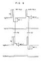
- The theoretical background of this invention will be described in the following.
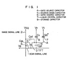
- The electric equivalent circuit of a display element of a TFT active matrix drive LCD is shown in Fig. 1. Each display element includes a
TFT 3 at the intersection between ascan signal line 1 andimage signal line 2. A TFT has as its parasitic capacitors a gate-drain capacitor Cgd 4, source-drain capacitor Csd 5 and gate-source capacitor Cgs 6. In addition, there are intentionally provided a liquid crystal capacitor Clc* 7 andstorage capacitor Cs 8. - As the drive voltages for the display element, a scan signal Vg is applied to the
scan signal line 1, an image signal voltage Vsig to theimage signal line 2, a modulating signal reversing its polarities Ve(+) and Ve(-) alternately for each field to one electrode of the storage capacitor Cs, and a voltage constant for all fields to the opposing electrode of the liquid crystal capacitor Clc*. The influence of the drive voltages is reflected upon the pixel electrode (at point A in Fig. 1) through electrostatic induction via the above-described parasitic capacitors and intentionally provided capacitors. - Upon application of the voltages Vg, Ve(+), Ve(-), Vt and Vsig for n-th scan line shown at (a) to (d) in Fig. 2 to the corresponding terminals shown in Fig. 1, the potential change ΔV* at the pixel electrode caused by the capacitive coupling is given by the following equations (1) and (2) respectively for the even and odd fields (excepting the potential change by the voltage from the image signal line upon turning-on of the TFT):
ΔV*⁺
= (CsVe(+) + CgdVg ± CsdVsig)/Ct (1)
ΔV*⁻
= (CsVe(-) - CgdVg ± CsdVsig)/Ct (2)
Ct = Cs + Cgd + Csd + Clc*
= Cp + Csd + Clc* = ΣC - The second terms of the equations (1) and (2) represent a potential change induced to the pixel electrode by the scan signal Vg via the parasitic capacitor Cgd. The first terms represent the effect of the first modulating voltage. The third terms represent a potential change induced to the pixel electrode by the image signal voltage via the parasitic capacitor. Clc* represents the capacitance of the liquid crystal which capacitance changes with the dielectric anisotropy as the orientation state of the liquid crystal changes with the amplitude of the signal voltage Vsig. ΔV* accordingly changes with the magnitude of the liquid crystal capacitance which may take a large value Clc(h) or small value Clc(l). The gate-source capacitor Cgs can be neglected because this capacitor does not directly influence the pixel electrode potential and also because both the scan signal line and image signal line are driven with low impedance power sources.
- If the potential changes ΔV*+ and ΔV*- at the even and odd fields are made equal, it is possible to compensate for the DC potential change given to the pixel electrode by the scan signal Vg via the parasitic capacitor Cgd. The DC potential is therefore not applied across the liquid crystal, thereby enabling symmetrical Ac drive. In other words, the following equation can be satisfied:
(CsVe(+) + CgdVg - CsdVsig) = (CsVe(-) - CgdVg - CsdVsig) (3)
Since the image signal voltage Vsig is reversed alternately for each scan line, the third term CsdVs is cancelled out at each field. Therefore, the equation (3) is simplified to the following equation:
(CsVe(+) + CgdVg) = (CsVe(-) - CgdVg) (4) - The first point to be notified is that the potential ΔV* induced to the pixel electrode relative to the opposing electrode can be made equal for even and odd fields, irrespective of the liquid crystal capacitance.
- The second point is that the term Clc* does not appear in the equations (3) and (4). In other words, if the liquid crystal is driven under the conditions satisfying the equations (3) and (4), the effects of the dielectric anisotropy of liquid crystal can be eliminated so that the DC voltage caused by Clc* is not generated within the display unit.
- The third point is that under the conditions satisfying the equations (3) and (4), it is possible to cancel out the DC voltage induced across the image signal line and pixel electrode by the scan signal Vg through the parasitic capacitor Cgd. According to the drive method of this invention, a signal is used which changes its polarity alternately for each field, between negative and positive relative to the opposing electrode potential, so that as viewed from the odd and even two fields, DC voltage field is not generated among the pixel electrode, signal electrode and opposing electrode. This drive method which generates no DC voltage across the liquid crystal, allows improved reliability.
- The fourth point to be noticed further is that the conditional equations (3) and (4) include two voltage parameters Ve(+) and Ve(-) which can be arbitrarily set on the side of the display unit. By properly setting the Ve(+) and Ve(-) values of the equations (3) and (4), the value of the potential change ΔV* at the pixel electrode can be arbitrarily set. If the value ΔV* is set larger than or equal to the threshold voltage of the liquid crystal, the signal Vsig of a smaller amplitude can be used. With a smaller amplitude signal Vsig, the amplitude of signals outputted from the image signal drive circuit dealing with analog signals can be made small so that the power consumption of the drive circuit can be reduced in proportion to the square of the amplitude. In case of a color display, the power consumed by a chroma IC also handling analog signals can be reduced. Since this IC is turned on and off by the digital modulating signals Ve(+) and Ve(-), all the drive circuits constructed of complementary MOSICs can also be operated with reduced drive power. The values of the above-described capacitors and voltage parameters used in the embodiment display units to be described later are as follows:
Cs = 0.68pF, Clc(h) = 0.226pF,
Clc(l) = 0.130pF, Cgd = 0.059pF,
Csd = 0.001pF, Vg = 15.5V, Ve(+) = -2.5V,
Ve(-) = +4.9V, Vt = 0V, Vsig = ±2.0V. - Upon taking into consideration of the above parameters, the third term of the equation (3) can be neglected and the equation (4) is changed to the equation (4a) which is given by:
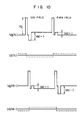
(Ve(-) - Ve(+)) = 2CgdVg/Cs (4a) - Waveforms shown at (e) and (f) in Fig. 1 represent the potential change at the pixel electrode (point A in Fig. 1) when the drive signal Vg, Vsig, and modulating signal Ve are applied to the electrode terminals shown in Fig. 1. Specifically, in the case where Vsig takes a phase as shown by a solid line at (d) in Fig. 1 relative to the modulating signal Ve, upon application of the scan signal Vg at T = T1 at the odd field, TFT becomes conductive and the potential Va at point A is charged to the potential Vs(h). The signal Ve changes in the negative direction by the amount Ve(-) at T = T2 before TFT turns off (preferably at the time between T1 and T2 during the conductive state of TFT). When the scan signal falls, this potential change of Vg appears as a potential change ΔVg at point A via the capacitor Cgd. When the signal Ve changes in the positive direction by the amount Ve(-), this causes the potential change at point A as shown at (d) in Fig. 2. When the signal Vsig changes from Vs(h) to Vs(l) at time T = T5, this causes the corresponding potential change as shown at (d) in Fig. 2. The potential change caused by these capacitive couplings is represented by ΔV*.
- Thereafter at the even field, upon application of the scan signal, TFT charges point A to the low level Vs(l) of the signal Vsig. Upon turning-off of TFT, the potential change caused by the capacitive couplings appears as ΔV* in the similar manner described above. As appreciated, in the case where Vsig and Ve take the above phase relationship, i.e., in the case where at the time of turning-off of TFT, Vsig takes a high level when VE takes a low level, and vice versa, the potential change Veff at the pixel electrode relative to the image signal amplitude Vsigpp, upon a change of the Ve after turning-on of Ve, becomes approximately 2ΔV*+ 2Vsigpp as shown at (e) in Fig. 2, Vsig and ΔV* being superposed one upon the other. In this case, the amplitude of an image signal from the image signal output IC can be reduced by 2ΔV* (hereinafter this phase relationship between Ve and Vsig is called the opposite phase).
- On the contrary, in the case where the modulating signal Ve and image signal Vsig take a phase relationship as shown at the broken line at (d) in Fig. 2 (hereinafter this phase relationship is called the same phase), the potential change at the pixel electrode becomes approximately 2ΔV* - 2Vsigpp, Vsig and ΔV* being cancelled out partially relative to each other.
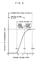
- Fig. 3 shows the relationship between a voltage applied to a liquid crystal and the transmission light intensity, and the voltage range for controlling the transmitted light with ΔV* and Vsig. The intensity of a transmitted light at liquid crystal changes within the voltage range from the threshold voltage Vth of liquid crystal to its saturation voltage Vmax. If ΔV* is set larger than or equal to Vth without amplitude and phase control of signal voltages, the maximum necessary image signal voltage becomes (Vmax - Vth). If on the other hand ΔV* is set at Vct with the amplitude and phase control of signal voltages, the maximum necessary image signal voltage can be reduced to about (Vmax - Vth)/2, thereby achieving one of the above-described objects of this invention which is to make smaller the image signal amplitude.
- Fig. 4 shows voltage waveforms aiming at improving the drive method shown in Fig. 2, wherein used is a voltage waveform indicated at (b) in Fig. 4 different from that in Fig. 2. The fundamental difference resides in that the voltage of Ve is set at different values between the period from T = T4 to T=1′ at the odd field and the period from T = T4′ to T1 at the even field. Specifically the modulating signal Ve is applied as in the following. The signal Ve is not changed at time T = T2 as indicated by a broken line circle at (b) in Fig. 4, but is changed at T = T4 in the positive direction by the amount Ve(-). The modulating signal is then changed slightly at time T = T2′ (within the period while TFT is turned on, or before TFT turns off) and thereafter, at time T = T4′ after the completion of scanning by the signal Vg (after TRT turns off), the modulating signal is changed in the negative direction by the amount Ve(+). As appreciated, it is possible to change the potential of the modulating signal during the turning-off period of TFT while satisfying the equation (4).
- If the voltage ΔV* of 3.4 V as in Fig. 3 is required upon application of the modulating signal, the modulating signal Ve is changed in the positive direction by the amount of 4.95 V at time T = T4, and in the negative direction by the amount of 2.50 V at time T = T3′, respectively in accordance with the equation (4a). The voltage difference 2.45 V therebetween is given by changing the potential Ve during the on-period of TFT as shown in Fig. 4.
- The invention will now be described more in detail with reference to the preferred embodiments.
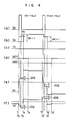
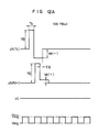
- The display unit of the first embodiment of this invention is shown in Fig. 5.
Reference numeral 11 designates a scan signal drive circuit, 12 an image signal drive circuit, 13 a first modulating circuit, and 14 a second modulating circuit. 15a, 15b, ..., 15z designates scan signal lines, 16a, 16b, ..., 16z image signal lines, 17a, 17b, ..., 17z common electrodes of storage capacitors Cs, and 18a, 18b, ..., 18z opposing electrodes of liquid crystals. - In this embodiment, storage capacitors and opposing electrodes are separated at each scan signal line. A modulating signal is applied to the common electrode of the storage capacitors at each scan signal line. The timing chart showing the scan signal and modulating signal is shown in Fig. 6. Shown in this timing chart are scan signals and modulating signals for the N-th and (N+1)-th scan signal lines. The relationship among the modulating signals, ΔV* and Vsig is essentially the same as that shown in Fig. 2. Namely, the polarities of the image signal and modulating signals are reversed alternately for each field.
- According to this embodiment, all the range from black to white could be driven bt a signal voltage with its amplitude only 3Vpp, while retaining a good display contrast with less flickers. The DC components among respective electrodes were almost zero with a good reliability of the liquid crystal for a long period. The brightness control of a display image was carried out by changing the amplitude of the modulating signal and hence of ΔV*.
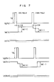
- In this embodiment, although the same circuit shown in Fig. 5 of the first embodiment is used, a voltage waveform of Ve shown in Fig. 7 is used which is different from that of the first embodiment. The voltage of Ve is different between the even and odd fields. The modulating signals Ve(N) and Ve(N+1) are changed two steps in the negative direction. Specifically, the Ve potential is changed during the on-period of TFT, and after TFT turns off, changed further in the negative direction by the amount smaller than the change in the positive direction.
- In addition to the advantages obtained by the first embodiment, this embodiment has another advantage that since the change of Ve in the negative direction during the on-period of TFT is small, the gate voltage necessary for a given image signal voltage is reduced.
- In this embodiment, although the same circuit of the first and second embodiments is used and the same voltage waveforms of Vg and Ve are used, the waveform of Vt at each scan line is reversed alternately for each field. The waveform of Vt changes its polarity during the on-period of TFT in the direction opposite to that the waveform Ve changes after the turning-off of TFT. With this arrangement, the modulating voltages Ve(+) and Ve(-) become smaller than those of the first and second embodiments.
- The circuit of the display unit of the fourth embodiment is shown in Fig. 8 and the voltage waveforms applied to this circuit are shown in Fig. 9. In Fig. 8, reference numeral 21a designates a first scan signal line, 21a′ a common electrode line of storage capacitors at the first scan signal line, 21z the last scan signal line, and 21z′ a scan signal line at the stage before the last stage. This embodiment is different from the first and second embodiments in that the common electrode of storage capacitors is connected to the scan line at the preceding stage. The modulating signal is therefore applied to the preceding stage scan signal line. As shown in Fig. 9, when a delay time τd lapses after scanning the (N+1)-th scan signal line, the polarity of the modulating signal applied to the N-th scan signal line is reversed.
- The polarity of the modulating signal may be reversed both for the N-th and (N+1)-th scan lines and for the even and odd fields, or only for the even and odd fields. The potential changes of the modulating signal by the amount Ve(+) in the positive direction and by the amount Ve(-) in the negative direction are made variable independently of each other.
- The advantages obtained by this embodiment are the same as those of the first embodiment.
- In this embodiment, the display unit having the same circuit as the fourth embodiment is driven by the signals having the waveforms shown in Fig. 10. In the fourth embodiment, the voltage Vg after modulation is the same for both the even and odd fields, whereas in this embodiment it is different between the even and odd fields. With the waveforms shown in Fig. 10, not only the advantages of the fourth embodiment are obtained, but also the gate amplitude required for driving the gate is made smaller.
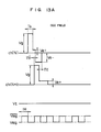
- The circuit of the display unit of the sixth embodiment is shown in Fig. 11, and the voltage waveforms applied to this circuit are shown in Fig. 12.
- This embodiment is the same as the fourth embodiment in that the modulating signal is applied to the scan signal line, but is different from the already described embodiments in that the opposing electrodes are not grouped into each scan signal line but all the electrodes within the display unit are supplied with a same potential, and in that the polarity of the potential between the pixel electrode and opposing electrode is changed alternately for each one scan period (1 H). In Fig. 11,
reference numeral 22 designates a scan signal drive circuit, 25 an image signal drive circuit, and 26 a second modulation signal generating circuit.Reference numerals - The potentials Ve(+) and VE(-) of the modulating signal immediately after the scan signal Vg in the waveforms Ch(N) and Ch(N+1) are changed independently of each other. The duration Ts of the scan signal Vg is made variable within the period smaller than one scan period. After the lapse of a delay time τd after scanning the succeeding stage Ch(N+1) scan line, the modulating signal is applied.
- By changing the potentials Ve(+) and Ve(-) of the modulating signal immediately after the scan signal independently of each other, the conditions of the equation (4a) can be satisfied.
- Also in this embodiment wherein the polarity of the potential at the pixel electrode is changed alternately for each one scan line, it is possible to compensate for the effects of the dielectric anisotropy of liquid crystal and of the DC voltage to be generated between the image signal line and pixel electrode, by adjusting the potentials Ve(+) and Ve(-) (it naturally follows that the average potential of image signals supplied to the image signal line becomes equal to that of pixel electrodes). Consequently, it is possible to remove the main causes of flickers and image memory phenomenon, improve the drive reliability, and reduce the drive power. The gradation controllability is also improved.
- Further, since all the opposing electrodes are maintained at the same potential, the number of second modulating signal output lines for the opposing electrodes can be reduced.
- Furthermore, since all the potentials of Vsigc of the image signal center voltage, opposing electrode potential Vtc, and Vpc of the pixel center potential can be made equal so that the DC components will become almost zero within the display unit.
- The occurrence of the image memory phenomenon was checked by displaying a fixed pattern such as window pattern, color bar, and resolution chart on the display unit and by using the drive method of this embodiment. After displaying a window pattern for four hours, the whole screen of the display unit was set at the halftone display condition. The burning phenomenon of the fixed pattern was not observed.
- The image burning phenomenon of two display panels driven in accordance with the conventional method was also checked for comparison therebetween. The first display panel has no storage capacitor for each pixel. With this display panel, the internal DC potential difference between the image signal line and pixel electrode induced by the scan signal via the parasitic capacitor Cgd is 3.5 to 4.0 V. After displaying a window pattern on this display panel for three minutes, the burning phenomenon was clearly observed. Also, after displaying a window pattern on this display panel for one hour, the burning phenomenon did not disappear for three hours. Other fixed patterns also resulted in the same burning phenomenon. The second display panel has a storage capacitor of 1 pF for each pixel, and the internal DC potential difference is 0.7 to 1.0 V. After displaying a fixed pattern for several minutes on this display panel, the burning phenomenon was not observed definitely, but after the one hour consecutive display, it was observed and continued thereafter for several hours.
- In this embodiment, the voltage waveforms of the fifth embodiment are used while the potential of the second modulating signal generator shown in Fig. 11 is made floated, i.e., while the opposing electrode are not connected to any circuit portion. In this case, the modulating signal Ve applied to the scan signal line is induced, via the internal electrostatic capacitor within the display unit, also to the opposing electrode. The image signal line is held at the potential irrelevant to the modulating signal Ve so that the amplitude of the second demodulating signal appearing at the opposing electrode is in general smaller than Ve, thereby not satisfying the conditional equation (4b′) correctly. However, the second modulating signal generator can be omitted, resulting in a large reduction of power consumption. An image of good quality can be displayed also in this case, satisfying almost all of the objects of the present invention.
- In this embodiment, the storage capacitor
common lines common lines - In this embodiment, the circuit shown in Fig. 11 is used and the voltage waveforms shown in Fig. 13 are applied to the display unit. The voltage waveforms Ch(N) and Ch(N+1) shown in Fig. 13 are modifications of those of the sixth embodiment shown in Fig. 12. Specifically, the voltage waveform Ch(N) in the odd field shown in Fig. 13A takes a potential Ve(+) after the on-period Ts of TFT, and after the lapse of a delay time τd′ (0 ≦ τd′ < Ts) after turning-on of TFT at the succeeding scan line as shown by Ch(N+1), takes a potential Ve(-). In the even field, the voltage waveform Ch(N+1) takes the same waveform as that of Ch(N) in the odd field. With the voltage waveforms shown in Fig. 13, it is possible that the potential change given to the succeeding pixel electrode during the on-period of TFT at the Ch(N) be made the same for both the even and odd fields. Flickers are thereby reduced more than that by the voltage waveforms shown in Fig. 12.
- This embodiment uses the circuit shown in Fig. 11 and the applied voltage waveforms shown in Fig. 14 which shows another modification of the voltage waveforms Ch(N) and Ch(N+1) of the sixth embodiment shown in Fig. 12. Specifically, the voltage waveform Ch(N) in the odd field shown in Fig. 14A takes a zero potential after the on-period Ts of TFT, and after the lapse of a delay time τd′ (0 ≦ τd′ < Ts) after turning-on of TFT at the succeeding scan line as shown by Ch(N+1), takes a potential Ve(-). On the other hand, the voltage waveform Ch(N+1) in the even field takes a zero potential after the on-period of TFT, and after the lapse of a delay time τd′ (0 ≦ τd′ < Ts) after turning-on of TFT at the succeeding scan line as shown by Ch(N+1), takes a potential Ve(+). Ch(N) in the odd field and Ch(N+1) in the even field are the same voltage waveform, and Ch(N) in the even field and Ch(N+1) in the odd field are the same voltage waveform. With the voltage waveforms shown in Fig. 14, it is possible that the potential change given to the succeeding pixel electrode during the on-period of TFT at the Ch(N) be made the same for both the even and odd field. Flickers are thereby reduced more than that by the voltage waveforms shown in Fig. 12.
- The ninth and tenth embodiments are modifications of the sixth embodiment, and the same advantages as the sixth embodiment are obtained by the ninth and tenth embodiments.
- As seen from the foregoing description, the present invention has the following distinctive advantages.
- First, the amplitude of voltage signals to be generated from the signal drive circuits in an active matrix display unit is considerably lowered, resulting in a reduction of power consumption by the drive circuits which deal with analog signals. Further, in the case of a color display, the amplitude of signals of chroma ICs are lowered to thus reduce power consumption. The drive power for the display unit as a whole can thus be reduced. The lower amplitude of voltage signals makes it easy to fabricate electronic circuitries which nowadays require more and more high integration and high frequency drive signals. In addition, the drive circuit can be operated within the region having a good linearity, thereby allowing a secondary advantage of improving the display quality.
- Second, the display quality can be improved. Even in AC driving the display unit alternately for each field as shown in the second and third embodiments, the causes of flickers can be eliminated. With the fourth embodiment, the display brightness can be made uniform and the gradation display performance can be considerably improved.
- Third, the reliability of a display unit can be improved, because there is removed the DC voltage conventionally generated unavoidably within the unit due to the anisotropy of liquid crystal, due to capacitive coupling of a scan signal via Cgd, or due to other causes. The DC voltage is the cause of inducing various display defects. By removing the DC voltage, there is less occurrence of the image burning phenomenon which might occur after the display of a fixed pattern. Further, the drive conditions satisfying the equation (4) are not adversely affected by the dielectric anisotropy of liquid crystal. This means that even if the dielectric constant itself changes, e.g., when a display unit is used within a broad temperature region, such change does not influence the operation of the display unit, thereby allowing a stable drive.
- In the above description, the present invention has been described using a liquid crystal display unit by way of example. The thought of this invention is applicable to driving other flat plate type display units.
- As appreciated above, according to the present invention, it is possible to considerably lower the output voltage signal amplitude of drive circuits for an active matrix display unit, to thereby reduce the power consumption by the drive circuits dealing with analog signals and improve both the image quality and reliability.
Claims (12)
CsVe(+) + CgdVg = CsVe(-) - CgdVg
where Cs is a storage capacitor, Cgd is a gate-drain capacitor and Csd is a source-drain capacitor of said thin film transistor.
Vth ≦ Δ V* ≦ Vmax
where ΔV* is expressed by:
ΔV* = (Ve(+) + Ve(-)) Cs/2Ct
Ct = Cs + Cgd + Csd + Clc
where the voltage range within which the transmission factor of a liquid crystal changes is from Vth to Vmax, Cs is the storage capacitor, Cgd is a gate-drain capacitor, Csd is a source-drain capacitor, and Clc is the liquid crystal capacitor.
ΔV* = (Vmax + Vth)/2
Applications Claiming Priority (2)
| Application Number | Priority Date | Filing Date | Title |
|---|---|---|---|
| JP63313456A JP2568659B2 (en) | 1988-12-12 | 1988-12-12 | Driving method of display device |
| JP313456/88 | 1988-12-12 |
Publications (3)
| Publication Number | Publication Date |
|---|---|
| EP0373565A2 true EP0373565A2 (en) | 1990-06-20 |
| EP0373565A3 EP0373565A3 (en) | 1991-09-11 |
| EP0373565B1 EP0373565B1 (en) | 1995-11-15 |
Family
ID=18041521
Family Applications (1)
| Application Number | Title | Priority Date | Filing Date |
|---|---|---|---|
| EP89122847A Expired - Lifetime EP0373565B1 (en) | 1988-12-12 | 1989-12-11 | Method of driving a display unit |
Country Status (5)
| Country | Link |
|---|---|
| US (1) | US5296847A (en) |
| EP (1) | EP0373565B1 (en) |
| JP (1) | JP2568659B2 (en) |
| KR (1) | KR920009030B1 (en) |
| DE (1) | DE68924836T2 (en) |
Cited By (18)
| Publication number | Priority date | Publication date | Assignee | Title |
|---|---|---|---|---|
| US5130829A (en) * | 1990-06-27 | 1992-07-14 | U.S. Philips Corporation | Active matrix liquid crystal display devices having a metal light shield for each switching device electrically connected to an adjacent row address conductor |
| US5151805A (en) * | 1989-11-28 | 1992-09-29 | Matsushita Electric Industrial Co., Ltd. | Capacitively coupled driving method for TFT-LCD to compensate for switching distortion and to reduce driving power |
| EP0535954A2 (en) * | 1991-10-04 | 1993-04-07 | Kabushiki Kaisha Toshiba | Liquid crystal display device |
| EP0536744A2 (en) * | 1991-10-09 | 1993-04-14 | Matsushita Electric Industrial Co., Ltd. | Driving method for a display device |
| EP0539185A1 (en) * | 1991-10-22 | 1993-04-28 | Sharp Kabushiki Kaisha | Driving apparatus and method for an active matrix type liquid crystal display apparatus |
| EP0588019A2 (en) * | 1992-07-21 | 1994-03-23 | Matsushita Electric Industrial Co., Ltd. | Active matrix liquid crystal display |
| EP0622655A2 (en) * | 1993-04-22 | 1994-11-02 | Matsushita Electric Industrial Co., Ltd. | Display device, method of driving the same and projection-type display apparatus using the same |
| EP0657864A1 (en) * | 1993-06-25 | 1995-06-14 | Hosiden Corporation | Method of ac-driving liquid crystal display, and the same using the method |
| WO1998027540A1 (en) * | 1996-12-19 | 1998-06-25 | Colorado Microdisplay, Inc. | Display system with modulation of an electrode voltage to alter state of the electro-optic layer |
| EP0907159A2 (en) * | 1997-06-13 | 1999-04-07 | Matsushita Electronic Components Co., Ltd. | Active matrix liquid crystal display panel and method of driving the same |
| US6329976B1 (en) | 1997-08-26 | 2001-12-11 | U.S. Philips Corporation | Electro-optical display device with temperature-dependent drive means |
| WO2002007142A1 (en) * | 2000-07-19 | 2002-01-24 | Matsushita Electric Industrial Co., Ltd. | Ocb liquid crystal display with active matrix and supplemental capacitors and driving method for the same |
| CN100356440C (en) * | 2001-07-16 | 2007-12-19 | 株式会社日立制作所 | Liquid crystal display device |
| CN101430466B (en) * | 2007-11-06 | 2010-12-01 | 瀚宇彩晶股份有限公司 | Pixel driving method, pixel driving device and liquid crystal display using thereof |
| US8188647B2 (en) | 1997-02-17 | 2012-05-29 | Seiko Epson Corporation | Current-driven light-emitting display apparatus and method of producing the same |
| CN102831871A (en) * | 2012-08-31 | 2012-12-19 | 京东方科技集团股份有限公司 | Display and image frame display method thereof |
| CN107195280A (en) * | 2017-07-31 | 2017-09-22 | 京东方科技集团股份有限公司 | A kind of pixel voltage compensation method, pixel voltage compensation system and display device |
| US11170726B2 (en) | 2009-12-18 | 2021-11-09 | Semiconductor Energy Laboratory Co., Ltd. | Method for driving liquid crystal display device |
Families Citing this family (77)
| Publication number | Priority date | Publication date | Assignee | Title |
|---|---|---|---|---|
| JP2950949B2 (en) * | 1990-08-28 | 1999-09-20 | 三洋電機株式会社 | Driving method of liquid crystal display device |
| JP2730286B2 (en) * | 1990-10-05 | 1998-03-25 | 松下電器産業株式会社 | Driving method of display device |
| JP2626451B2 (en) * | 1993-03-23 | 1997-07-02 | 日本電気株式会社 | Driving method of liquid crystal display device |
| JPH06289817A (en) * | 1993-04-01 | 1994-10-18 | Sharp Corp | Method and circuit for driving display device |
| TW270198B (en) * | 1994-06-21 | 1996-02-11 | Hitachi Seisakusyo Kk | |
| US5528256A (en) * | 1994-08-16 | 1996-06-18 | Vivid Semiconductor, Inc. | Power-saving circuit and method for driving liquid crystal display |
| US5986631A (en) * | 1995-07-05 | 1999-11-16 | Matsushita Electric Industrial Co., Ltd. | Method for driving active matrix LCD using only three voltage levels |
| KR100230793B1 (en) * | 1995-07-28 | 1999-11-15 | 김영환 | Driving method of lcd |
| TW315456B (en) * | 1995-11-06 | 1997-09-11 | Matsushita Electric Ind Co Ltd | |
| JP3069280B2 (en) * | 1995-12-12 | 2000-07-24 | 松下電器産業株式会社 | Active matrix type liquid crystal display device and driving method thereof |
| JP3037886B2 (en) * | 1995-12-18 | 2000-05-08 | インターナショナル・ビジネス・マシーンズ・コーポレイション | Driving method of liquid crystal display device |
| US6911962B1 (en) | 1996-03-26 | 2005-06-28 | Semiconductor Energy Laboratory Co., Ltd. | Driving method of active matrix display device |
| JP4307574B2 (en) * | 1996-09-03 | 2009-08-05 | 株式会社半導体エネルギー研究所 | Active matrix display device |
| US6046716A (en) | 1996-12-19 | 2000-04-04 | Colorado Microdisplay, Inc. | Display system having electrode modulation to alter a state of an electro-optic layer |
| US6078303A (en) | 1996-12-19 | 2000-06-20 | Colorado Microdisplay, Inc. | Display system having electrode modulation to alter a state of an electro-optic layer |
| CN100533528C (en) | 1997-02-17 | 2009-08-26 | 精工爱普生株式会社 | Display device |
| US6140993A (en) * | 1998-06-16 | 2000-10-31 | Atmel Corporation | Circuit for transferring high voltage video signal without signal loss |
| TW512303B (en) | 1998-08-21 | 2002-12-01 | Dar Chyi Technology Corp | Driving method of liquid crystal display |
| US6868154B1 (en) * | 1999-08-02 | 2005-03-15 | Robert O. Stuart | System and method for providing a service to a customer via a communication link |
| JP2001249319A (en) * | 2000-03-02 | 2001-09-14 | Hitachi Ltd | Liquid crystal display device |
| JPWO2001073738A1 (en) * | 2000-03-30 | 2004-01-08 | セイコーエプソン株式会社 | Display device |
| US6909415B2 (en) * | 2000-04-24 | 2005-06-21 | Matsushita Electric Industrial Co., Ltd. | Display unit and drive method therefor |
| JP3723747B2 (en) * | 2000-06-16 | 2005-12-07 | 松下電器産業株式会社 | Display device and driving method thereof |
| AU2002210928A1 (en) * | 2000-10-25 | 2002-05-06 | Matsushita Electric Industrial Co., Ltd. | Liquid crystal display drive method and liquid crystal display |
| JP2002333870A (en) | 2000-10-31 | 2002-11-22 | Matsushita Electric Ind Co Ltd | Liquid crystal display device, el display device and drive method therefor and display pattern evaluation method of subpixel |
| JP3832240B2 (en) | 2000-12-22 | 2006-10-11 | セイコーエプソン株式会社 | Driving method of liquid crystal display device |
| JP2002278517A (en) * | 2001-03-15 | 2002-09-27 | Hitachi Ltd | Liquid crystal display |
| US20020190942A1 (en) * | 2001-06-06 | 2002-12-19 | Lee Yu-Tuan | Driving method for thin film transistor liquid crystal display |
| JP2003005720A (en) * | 2001-06-21 | 2003-01-08 | Matsushita Electric Ind Co Ltd | Liquid crystal display method, liquid crystal display device, program, and medium |
| JP2003122358A (en) * | 2001-10-11 | 2003-04-25 | Sega Corp | Sound signal output method, and sound signal generating device and program |
| JP2005062396A (en) | 2003-08-11 | 2005-03-10 | Sony Corp | Display device and method for driving the same |
| JP2004046235A (en) * | 2003-09-05 | 2004-02-12 | Matsushita Electric Ind Co Ltd | Liquid crystal display device |
| US20050140634A1 (en) | 2003-12-26 | 2005-06-30 | Nec Corporation | Liquid crystal display device, and method and circuit for driving liquid crystal display device |
| JP4555063B2 (en) * | 2003-12-26 | 2010-09-29 | Nec液晶テクノロジー株式会社 | Liquid crystal display device, driving method and driving circuit thereof |
| EP1719104A1 (en) * | 2004-02-19 | 2006-11-08 | Koninklijke Philips Electronics N.V. | Display unit |
| TWI284879B (en) * | 2004-06-08 | 2007-08-01 | Fujitsu Ltd | Liquid crystal display apparatus and driving method thereof |
| US8836621B2 (en) | 2004-12-15 | 2014-09-16 | Nlt Technologies, Ltd. | Liquid crystal display apparatus, driving method for same, and driving circuit for same |
| JP4580775B2 (en) * | 2005-02-14 | 2010-11-17 | 株式会社 日立ディスプレイズ | Display device and driving method thereof |
| JP4843268B2 (en) * | 2005-07-08 | 2011-12-21 | 東芝モバイルディスプレイ株式会社 | Method for driving liquid crystal display device and liquid crystal display device |
| US8866717B2 (en) | 2005-08-18 | 2014-10-21 | Japan Display, Inc. | Display device and drive method providing improved signal linearity |
| TWI449009B (en) * | 2005-12-02 | 2014-08-11 | Semiconductor Energy Lab | Display device and electronic device using the same |
| KR20070078522A (en) * | 2006-01-27 | 2007-08-01 | 삼성전자주식회사 | Display device and liquid crystal display |
| KR101246830B1 (en) * | 2006-06-09 | 2013-03-28 | 삼성디스플레이 주식회사 | Display device and method of driving the same |
| JP2008015282A (en) * | 2006-07-06 | 2008-01-24 | Toshiba Matsushita Display Technology Co Ltd | Liquid crystal display |
| KR101337261B1 (en) * | 2006-07-24 | 2013-12-05 | 삼성디스플레이 주식회사 | Liquid crystal display and driving method thereof |
| JP4241781B2 (en) | 2006-08-10 | 2009-03-18 | エプソンイメージングデバイス株式会社 | Electro-optical device, drive circuit, and electronic device |
| JP5186913B2 (en) | 2007-01-22 | 2013-04-24 | セイコーエプソン株式会社 | Source driver, electro-optical device and electronic apparatus |
| US7928941B2 (en) | 2007-03-20 | 2011-04-19 | Sony Corporation | Electro-optical device, driving circuit and electronic apparatus |
| JP4428401B2 (en) * | 2007-05-21 | 2010-03-10 | エプソンイメージングデバイス株式会社 | Electro-optical device, drive circuit, and electronic device |
| US7830346B2 (en) * | 2007-07-12 | 2010-11-09 | Au Optronics Corporation | Liquid crystal display panel with color washout improvement by scanning line coupling and applications of same |
| TWI390279B (en) | 2007-08-30 | 2013-03-21 | Japan Display West Inc | Display apparatus and electronic equipment |
| JP5137744B2 (en) | 2007-08-30 | 2013-02-06 | 株式会社ジャパンディスプレイウェスト | Display device, driving method thereof, and electronic apparatus |
| JP5072489B2 (en) | 2007-08-30 | 2012-11-14 | 株式会社ジャパンディスプレイウェスト | Display device, driving method thereof, and electronic apparatus |
| WO2009034741A1 (en) | 2007-09-11 | 2009-03-19 | Sharp Kabushiki Kaisha | Display device, its driving circuit, and driving method |
| JP2009198981A (en) * | 2008-02-25 | 2009-09-03 | Seiko Epson Corp | Driving circuit of electrooptical device, driving method of electrooptical device, electrooptical device and electronic apparatus |
| CN101960510A (en) * | 2008-03-11 | 2011-01-26 | 夏普株式会社 | Drive circuit, drive method, liquid crystal display panel, liquid crystal module, and liquid crystal display device |
| GB2458957B (en) * | 2008-04-04 | 2010-11-24 | Sony Corp | Liquid crystal display module |
| US7916108B2 (en) * | 2008-04-21 | 2011-03-29 | Au Optronics Corporation | Liquid crystal display panel with color washout improvement and applications of same |
| JP2009300530A (en) * | 2008-06-10 | 2009-12-24 | Seiko Epson Corp | Driving device and method for electrooptical device, and electrooptical device and electronic equipment |
| JP2010008576A (en) * | 2008-06-25 | 2010-01-14 | Toshiba Mobile Display Co Ltd | Liquid crystal display, and method of driving liquid crystal display |
| US20100007591A1 (en) * | 2008-07-10 | 2010-01-14 | Himax Display, Inc. | Pixel unit for a display device and driving method thereof |
| TWI390498B (en) * | 2008-07-21 | 2013-03-21 | Chimei Innolux Corp | Amlcd and lcd panel |
| US8654288B2 (en) * | 2008-08-05 | 2014-02-18 | Sharp Kabushiki Kaisha | Method for manufacturing liquid crystal display device including forming alignment sustaining layers |
| JP2010197417A (en) * | 2009-02-23 | 2010-09-09 | Toppoly Optoelectronics Corp | Display device and electronic apparatus equipped with same |
| US20120086700A1 (en) * | 2009-06-29 | 2012-04-12 | Sharp Kabushiki Kaisha | Display Device And Method For Driving Same |
| WO2011033810A1 (en) * | 2009-09-16 | 2011-03-24 | シャープ株式会社 | Memory device, display device equipped with memory device, drive method for memory device, and drive method for display device |
| US20120274615A1 (en) * | 2009-11-13 | 2012-11-01 | Pioneer Corporation | Active matrix type module and driving method of active matrix type module |
| US20110234605A1 (en) * | 2010-03-26 | 2011-09-29 | Nathan James Smith | Display having split sub-pixels for multiple image display functions |
| US8633889B2 (en) | 2010-04-15 | 2014-01-21 | Semiconductor Energy Laboratory Co., Ltd. | Display device, driving method thereof, and electronic appliance |
| TWI534773B (en) | 2010-04-23 | 2016-05-21 | 半導體能源研究所股份有限公司 | Method for driving display device |
| GB2481008A (en) | 2010-06-07 | 2011-12-14 | Sharp Kk | Active storage pixel memory |
| JP5189149B2 (en) * | 2010-09-17 | 2013-04-24 | 奇美電子股▲ふん▼有限公司 | Active matrix display device and electronic apparatus having the same |
| US8896512B2 (en) | 2011-08-04 | 2014-11-25 | Sharp Kabushiki Kaisha | Display device for active storage pixel inversion and method of driving the same |
| US8836680B2 (en) | 2011-08-04 | 2014-09-16 | Sharp Kabushiki Kaisha | Display device for active storage pixel inversion and method of driving the same |
| US9142167B2 (en) * | 2011-12-29 | 2015-09-22 | Intel Corporation | Thin-film transitor backplane for displays |
| US20130328758A1 (en) * | 2012-06-08 | 2013-12-12 | Apple Inc. | Differential active-matrix displays |
| KR102170439B1 (en) * | 2013-09-09 | 2020-10-29 | 삼성디스플레이 주식회사 | Apparatus for detecting candidate region for afterimage and appratus for preventing afterimage including the same |
Citations (3)
| Publication number | Priority date | Publication date | Assignee | Title |
|---|---|---|---|---|
| EP0112700A2 (en) * | 1982-12-25 | 1984-07-04 | Kabushiki Kaisha Toshiba | Thin-film transistor circuit |
| US4675667A (en) * | 1983-09-21 | 1987-06-23 | Canon Kabushiki Kaisha | Method for driving liquid-crystal panel |
| GB2188471A (en) * | 1986-03-19 | 1987-09-30 | Sharp Kk | L C D devices |
Family Cites Families (16)
| Publication number | Priority date | Publication date | Assignee | Title |
|---|---|---|---|---|
| DE2953769C2 (en) * | 1978-02-08 | 1985-02-14 | Sharp K.K., Osaka | Liquid crystal display matrix with thin film transistor arrangement |
| JPS5957288A (en) * | 1982-09-27 | 1984-04-02 | シチズン時計株式会社 | Driving of matrix display |
| JPS603698A (en) * | 1983-06-21 | 1985-01-10 | ソニー株式会社 | Liquid crystal display |
| JPS6039620A (en) * | 1983-08-12 | 1985-03-01 | Asahi Glass Co Ltd | Image display device |
| JPS6083477A (en) * | 1983-10-13 | 1985-05-11 | Sharp Corp | Driving circuit of liquid crystal display device |
| JPS60151615A (en) * | 1984-01-19 | 1985-08-09 | Matsushita Electric Ind Co Ltd | Driving method of liquid-crystal display device |
| US4728172A (en) * | 1984-08-08 | 1988-03-01 | Energy Conversion Devices, Inc. | Subassemblies for displays having pixels with two portions and capacitors |
| JPS60156095A (en) * | 1984-11-22 | 1985-08-16 | ソニー株式会社 | Liquid crystal display unit |
| JP2583211B2 (en) * | 1985-05-10 | 1997-02-19 | シチズン時計株式会社 | Liquid crystal display |
| JPS61275823A (en) * | 1985-05-31 | 1986-12-05 | Seiko Epson Corp | Liquid crystal display device |
| JPS61275822A (en) * | 1985-05-31 | 1986-12-05 | Seiko Epson Corp | Liquid crystal display device |
| JPS61275824A (en) * | 1985-05-31 | 1986-12-05 | Seiko Epson Corp | Liquid crystal display device |
| JPS63249896A (en) * | 1987-04-06 | 1988-10-17 | 松下電器産業株式会社 | Liquid crystal display device |
| US4955697A (en) * | 1987-04-20 | 1990-09-11 | Hitachi, Ltd. | Liquid crystal display device and method of driving the same |
| KR920007167B1 (en) * | 1987-04-20 | 1992-08-27 | 가부시기가이샤 히다씨세이사구쇼 | Liquid crystal display apparatus and the method of driving the same |
| JP2737209B2 (en) * | 1988-03-11 | 1998-04-08 | 松下電器産業株式会社 | Driving method of display device |
-
1988
- 1988-12-12 JP JP63313456A patent/JP2568659B2/en not_active Expired - Lifetime
-
1989
- 1989-12-11 EP EP89122847A patent/EP0373565B1/en not_active Expired - Lifetime
- 1989-12-11 DE DE68924836T patent/DE68924836T2/en not_active Expired - Lifetime
- 1989-12-12 KR KR1019890018362A patent/KR920009030B1/en not_active IP Right Cessation
-
1992
- 1992-06-22 US US07/902,564 patent/US5296847A/en not_active Expired - Lifetime
Patent Citations (3)
| Publication number | Priority date | Publication date | Assignee | Title |
|---|---|---|---|---|
| EP0112700A2 (en) * | 1982-12-25 | 1984-07-04 | Kabushiki Kaisha Toshiba | Thin-film transistor circuit |
| US4675667A (en) * | 1983-09-21 | 1987-06-23 | Canon Kabushiki Kaisha | Method for driving liquid-crystal panel |
| GB2188471A (en) * | 1986-03-19 | 1987-09-30 | Sharp Kk | L C D devices |
Non-Patent Citations (1)
| Title |
|---|
| JAPAN DISPLAY'86, 1986, pages 192-195; T. YANAGISAWA et al.: "Compensation of the display electrode voltage distortion" * |
Cited By (34)
| Publication number | Priority date | Publication date | Assignee | Title |
|---|---|---|---|---|
| US5151805A (en) * | 1989-11-28 | 1992-09-29 | Matsushita Electric Industrial Co., Ltd. | Capacitively coupled driving method for TFT-LCD to compensate for switching distortion and to reduce driving power |
| US5130829A (en) * | 1990-06-27 | 1992-07-14 | U.S. Philips Corporation | Active matrix liquid crystal display devices having a metal light shield for each switching device electrically connected to an adjacent row address conductor |
| EP0535954A2 (en) * | 1991-10-04 | 1993-04-07 | Kabushiki Kaisha Toshiba | Liquid crystal display device |
| EP0535954A3 (en) * | 1991-10-04 | 1994-02-09 | Toshiba Kk | |
| US5686932A (en) * | 1991-10-04 | 1997-11-11 | Kabushiki Kaisha Toshiba | Compensative driving method type liquid crystal display device |
| US5398043A (en) * | 1991-10-09 | 1995-03-14 | Matsushita Electric Industrial Co. Ltd. | Driving method for a display device |
| EP0536744A2 (en) * | 1991-10-09 | 1993-04-14 | Matsushita Electric Industrial Co., Ltd. | Driving method for a display device |
| EP0536744A3 (en) * | 1991-10-09 | 1993-08-04 | Matsushita Electric Industrial Co., Ltd. | Driving method for a display device |
| EP0539185A1 (en) * | 1991-10-22 | 1993-04-28 | Sharp Kabushiki Kaisha | Driving apparatus and method for an active matrix type liquid crystal display apparatus |
| US5598177A (en) * | 1991-10-22 | 1997-01-28 | Sharp Kabushiki Kaisha | Driving apparatus and method for an active matrix type liquid crystal display apparatus |
| EP0588019A3 (en) * | 1992-07-21 | 1994-09-21 | Matsushita Electric Ind Co Ltd | Active matrix liquid crystal display |
| EP0588019A2 (en) * | 1992-07-21 | 1994-03-23 | Matsushita Electric Industrial Co., Ltd. | Active matrix liquid crystal display |
| EP0622655A3 (en) * | 1993-04-22 | 1995-09-13 | Matsushita Electric Ind Co Ltd | Display device, method of driving the same and projection-type display apparatus using the same. |
| EP0622655A2 (en) * | 1993-04-22 | 1994-11-02 | Matsushita Electric Industrial Co., Ltd. | Display device, method of driving the same and projection-type display apparatus using the same |
| US6177965B1 (en) | 1993-04-22 | 2001-01-23 | Matsushita Electric Industrial Co., Ltd. | Display device and projection-type display apparatus using the device |
| EP0657864A1 (en) * | 1993-06-25 | 1995-06-14 | Hosiden Corporation | Method of ac-driving liquid crystal display, and the same using the method |
| EP0657864A4 (en) * | 1993-06-25 | 1995-12-13 | Hosiden Corp | Method of ac-driving liquid crystal display, and the same using the method. |
| US5784039A (en) * | 1993-06-25 | 1998-07-21 | Hosiden Corporation | Liquid crystal display AC-drive method and liquid crystal display using the same |
| WO1998027540A1 (en) * | 1996-12-19 | 1998-06-25 | Colorado Microdisplay, Inc. | Display system with modulation of an electrode voltage to alter state of the electro-optic layer |
| US8188647B2 (en) | 1997-02-17 | 2012-05-29 | Seiko Epson Corporation | Current-driven light-emitting display apparatus and method of producing the same |
| US8362489B2 (en) | 1997-02-17 | 2013-01-29 | Seiko Epson Corporation | Current-driven light-emitting display apparatus and method of producing the same |
| EP0907159A2 (en) * | 1997-06-13 | 1999-04-07 | Matsushita Electronic Components Co., Ltd. | Active matrix liquid crystal display panel and method of driving the same |
| EP0907159A3 (en) * | 1997-06-13 | 1999-06-09 | Matsushita Electronic Components Co., Ltd. | Active matrix liquid crystal display panel and method of driving the same |
| US6329976B1 (en) | 1997-08-26 | 2001-12-11 | U.S. Philips Corporation | Electro-optical display device with temperature-dependent drive means |
| WO2002007142A1 (en) * | 2000-07-19 | 2002-01-24 | Matsushita Electric Industrial Co., Ltd. | Ocb liquid crystal display with active matrix and supplemental capacitors and driving method for the same |
| US8130187B2 (en) | 2000-07-19 | 2012-03-06 | Toshiba Matsushita Display Technology Co., Ltd. | OCB liquid crystal display with active matrix and supplemental capacitors and driving method for the same |
| CN100356440C (en) * | 2001-07-16 | 2007-12-19 | 株式会社日立制作所 | Liquid crystal display device |
| CN101430466B (en) * | 2007-11-06 | 2010-12-01 | 瀚宇彩晶股份有限公司 | Pixel driving method, pixel driving device and liquid crystal display using thereof |
| US11170726B2 (en) | 2009-12-18 | 2021-11-09 | Semiconductor Energy Laboratory Co., Ltd. | Method for driving liquid crystal display device |
| CN102831871A (en) * | 2012-08-31 | 2012-12-19 | 京东方科技集团股份有限公司 | Display and image frame display method thereof |
| CN102831871B (en) * | 2012-08-31 | 2015-06-24 | 京东方科技集团股份有限公司 | Display and image frame display method thereof |
| CN107195280A (en) * | 2017-07-31 | 2017-09-22 | 京东方科技集团股份有限公司 | A kind of pixel voltage compensation method, pixel voltage compensation system and display device |
| CN107195280B (en) * | 2017-07-31 | 2020-12-29 | 京东方科技集团股份有限公司 | Pixel voltage compensation method, pixel voltage compensation system and display device |
| US11410628B2 (en) | 2017-07-31 | 2022-08-09 | Boe Technology Group Co., Ltd. | Pixel voltage compensation method for liquid crystal display to suppress pixel electrode voltage cross-talk |
Also Published As
| Publication number | Publication date |
|---|---|
| JP2568659B2 (en) | 1997-01-08 |
| JPH02157815A (en) | 1990-06-18 |
| EP0373565B1 (en) | 1995-11-15 |
| DE68924836D1 (en) | 1995-12-21 |
| EP0373565A3 (en) | 1991-09-11 |
| KR920009030B1 (en) | 1992-10-12 |
| DE68924836T2 (en) | 1996-07-04 |
| US5296847A (en) | 1994-03-22 |
| KR900010633A (en) | 1990-07-09 |
Similar Documents
| Publication | Publication Date | Title |
|---|---|---|
| US5296847A (en) | Method of driving display unit | |
| US5706023A (en) | Method of driving an image display device by driving display materials with alternating current | |
| US5151805A (en) | Capacitively coupled driving method for TFT-LCD to compensate for switching distortion and to reduce driving power | |
| JP2806098B2 (en) | Driving method of display device | |
| US5995074A (en) | Driving method of liquid crystal display device | |
| US7193601B2 (en) | Active matrix liquid crystal display | |
| US7973757B2 (en) | Liquid crystal display | |
| US7321352B2 (en) | Liquid crystal display and method for driving the same | |
| EP0216168A2 (en) | Method of driving a display panel | |
| JPH05165431A (en) | Driving method for liquid crystal display device | |
| EP0436384B1 (en) | A driving circuit for a liquid crystal display apparatus | |
| JP2737209B2 (en) | Driving method of display device | |
| JP2730286B2 (en) | Driving method of display device | |
| KR20040009817A (en) | A liquid crystal display apparatus | |
| JP2629360B2 (en) | Driving method of liquid crystal display device | |
| JP3140088B2 (en) | Driving method of liquid crystal display device | |
| JPH0580354A (en) | Liquid crystal display device | |
| KR20030021873A (en) | device for driving liquid crystal display | |
| KR100443830B1 (en) | Liquid Crystal Display and Driving Method Thereof | |
| JPH05210088A (en) | Driving method for liquid crystal display device | |
| KR100617611B1 (en) | Circuit for yielding gate signal with multi-level in thin film transistor liquid crystal display | |
| KR100205427B1 (en) | Data sampling-holded circuit and its driving method for liquid crystal display device | |
| JPH0343786A (en) | Signal processing circuit for active matrix liquid crystal panel | |
| JPH0519235A (en) | Method for driving liquid crystal display device | |
| JPH0667146A (en) | Method for driving liquid crystal display device |
Legal Events
| Date | Code | Title | Description |
|---|---|---|---|
| PUAI | Public reference made under article 153(3) epc to a published international application that has entered the european phase |
Free format text: ORIGINAL CODE: 0009012 |
|
| AK | Designated contracting states |
Kind code of ref document: A2 Designated state(s): DE FR GB |
|
| 17P | Request for examination filed |
Effective date: 19901228 |
|
| PUAL | Search report despatched |
Free format text: ORIGINAL CODE: 0009013 |
|
| AK | Designated contracting states |
Kind code of ref document: A3 Designated state(s): DE FR GB |
|
| 17Q | First examination report despatched |
Effective date: 19930908 |
|
| GRAA | (expected) grant |
Free format text: ORIGINAL CODE: 0009210 |
|
| AK | Designated contracting states |
Kind code of ref document: B1 Designated state(s): DE FR GB |
|
| REF | Corresponds to: |
Ref document number: 68924836 Country of ref document: DE Date of ref document: 19951221 |
|
| ET | Fr: translation filed | ||
| PLBE | No opposition filed within time limit |
Free format text: ORIGINAL CODE: 0009261 |
|
| STAA | Information on the status of an ep patent application or granted ep patent |
Free format text: STATUS: NO OPPOSITION FILED WITHIN TIME LIMIT |
|
| 26N | No opposition filed | ||
| REG | Reference to a national code |
Ref country code: GB Ref legal event code: IF02 |
|
| REG | Reference to a national code |
Ref country code: GB Ref legal event code: 746 Effective date: 20031002 |
|
| REG | Reference to a national code |
Ref country code: FR Ref legal event code: D6 |
|
| REG | Reference to a national code |
Ref country code: GB Ref legal event code: 732E |
|
| REG | Reference to a national code |
Ref country code: FR Ref legal event code: TP |
|
| PGFP | Annual fee paid to national office [announced via postgrant information from national office to epo] |
Ref country code: DE Payment date: 20081205 Year of fee payment: 20 |
|
| PGFP | Annual fee paid to national office [announced via postgrant information from national office to epo] |
Ref country code: GB Payment date: 20081210 Year of fee payment: 20 |
|
| REG | Reference to a national code |
Ref country code: GB Ref legal event code: PE20 Expiry date: 20091210 |
|
| PG25 | Lapsed in a contracting state [announced via postgrant information from national office to epo] |
Ref country code: GB Free format text: LAPSE BECAUSE OF EXPIRATION OF PROTECTION Effective date: 20091210 |
|
| PGFP | Annual fee paid to national office [announced via postgrant information from national office to epo] |
Ref country code: FR Payment date: 20080830 Year of fee payment: 20 |