EP0376285A2 - Microcomputer having electrically erasable and programmable nonvolatile memory - Google Patents
Microcomputer having electrically erasable and programmable nonvolatile memory Download PDFInfo
- Publication number
- EP0376285A2 EP0376285A2 EP89124030A EP89124030A EP0376285A2 EP 0376285 A2 EP0376285 A2 EP 0376285A2 EP 89124030 A EP89124030 A EP 89124030A EP 89124030 A EP89124030 A EP 89124030A EP 0376285 A2 EP0376285 A2 EP 0376285A2
- Authority
- EP
- European Patent Office
- Prior art keywords
- data
- data write
- write process
- signal
- memory cell
- Prior art date
- Legal status (The legal status is an assumption and is not a legal conclusion. Google has not performed a legal analysis and makes no representation as to the accuracy of the status listed.)
- Granted
Links
- 238000000034 method Methods 0.000 claims abstract description 35
- 238000007864 suspending Methods 0.000 claims abstract description 6
- 230000004044 response Effects 0.000 description 21
- 238000005086 pumping Methods 0.000 description 11
- 208000037656 Respiratory Sounds Diseases 0.000 description 5
- 238000010586 diagram Methods 0.000 description 5
- 206010037833 rales Diseases 0.000 description 5
- 238000001514 detection method Methods 0.000 description 3
- 239000003990 capacitor Substances 0.000 description 1
- 238000010276 construction Methods 0.000 description 1
- 230000005669 field effect Effects 0.000 description 1
- 238000007667 floating Methods 0.000 description 1
- 230000002093 peripheral effect Effects 0.000 description 1
- 238000004886 process control Methods 0.000 description 1
- 230000002035 prolonged effect Effects 0.000 description 1
- 230000003068 static effect Effects 0.000 description 1
Images


Classifications
-
- G—PHYSICS
- G11—INFORMATION STORAGE
- G11C—STATIC STORES
- G11C16/00—Erasable programmable read-only memories
- G11C16/02—Erasable programmable read-only memories electrically programmable
- G11C16/06—Auxiliary circuits, e.g. for writing into memory
- G11C16/30—Power supply circuits
-
- G—PHYSICS
- G11—INFORMATION STORAGE
- G11C—STATIC STORES
- G11C16/00—Erasable programmable read-only memories
- G11C16/02—Erasable programmable read-only memories electrically programmable
- G11C16/06—Auxiliary circuits, e.g. for writing into memory
- G11C16/08—Address circuits; Decoders; Word-line control circuits
-
- G—PHYSICS
- G11—INFORMATION STORAGE
- G11C—STATIC STORES
- G11C16/00—Erasable programmable read-only memories
- G11C16/02—Erasable programmable read-only memories electrically programmable
- G11C16/06—Auxiliary circuits, e.g. for writing into memory
- G11C16/32—Timing circuits
-
- G—PHYSICS
- G11—INFORMATION STORAGE
- G11C—STATIC STORES
- G11C2216/00—Indexing scheme relating to G11C16/00 and subgroups, for features not directly covered by these groups
- G11C2216/12—Reading and writing aspects of erasable programmable read-only memories
- G11C2216/20—Suspension of programming or erasing cells in an array in order to read other cells in it
Definitions
- the present invention relates to a microcomputer and, more particularly, to a microcomputer having an electrically erasable and programmable nonvolatile memory (called hereinafter "E2PROM”) as a data memory.
- E2PROM electrically erasable and programmable nonvolatile memory
- RAM random access memory
- E2PROM is employed as a part of that data memory to store and hold data which are required to be kept stored even after a power voltage is cut off.
- a data write process to E2PROM consists of an erasing operation, which is first performed to initialize the memory cell at an address to be written with new data by erasing the data formerly stored at that address, and a writing operation, which is subsequently performed to write the new data into that address.
- the erasing and writing operations require a relatively long time duration, about 10 msec, respectively. This time duration is extremely long in comparison with an instruction execution time or a maching cycle time of CPU (Central Processing Unit). If CPU is programmed to perform the data write process to E2PROM, the execution efficiency of the program is deteriorated remarkably.
- an erasing and writing automaton circuit is provided to control the data write process to E2PROM in place of CPU.
- CPU receives a data write instruction to E2PROM, it issues the automaton circuit with a data write request including a write address information, data to be written (i.e., write data) and a write command signal.
- CPU is thereafter shifted to a subsequent operation to execute other instructions.
- the erasing and writing automaton circuit is initiated by the data write request to first perform the erasing operation in which a so-called Vpp voltage higher than a power voltage applied to the CPU is applied to memory cells of the selected address of E2PROM for the above-mentioned relatively long period.
- the data which have been stored in those memory cells, are thereby erased.
- the writing operation is performed to apply the Vpp voltage or ground voltage to the selected memory cells in accordance with data to be written for the relatively long period.
- the new data is thereby stored in the selected memory cells.
- the automaton circuit In order to detect each of the erasing and writing operation time durations, the automaton circuit includes a timer for counting a reference clock signal and to generate an operation end signal when a predetermine time has elapsed. In response to this operation end signal, the application of the Vpp voltage to the selected memory cells is terminated to thereby complete the erasing and writing operations.
- the data write process may be temporarily suspended by the data read request issued from CPU.
- the automaton circuit automatically completes the erasing and writing operations in response to the operation end signal generated by the timer. For this reason, the application time of the Vpp voltage to the selected memory cells is shortened by the suspended time of the data write process. The data is thereby not substantially written into E2PROM.
- This drawback can be solved by initializing or resetting the timer in response to the data read request. However, in that case, the data write process is again performed from the beginning, so that a time for preforming the data write process is prolonged undesirably.
- an object of the present invention is to provide a microcomputer including E2PROM equipped with an improved data erasing, writing and read control circuit.
- Another object of the present invention is to provide a microcomputer having E2PROM into which data is surely written without prolonging a data write processing time.
- Still another object of the present invention is to provide an E2PROM equipped with a control circuit which performs a data write process to surely write data into selected memory cells without prolonging a processing time even when a data read request is issued during the data write processing operation.
- a microcomputer comprises E2PROM, CPU executing a program and issuing a data write request and a data read request to E2PROM, and a data/erasing/writing/reading control circuit including a timer counting a time to generate a processing end signal when a predetermined time has elapsed, a data write process control circuit responding to the data write request to perform a data write process in which data stored in a selected memory cell of E2PROM is first erased and new data is then written into the selected memory cell and responding to the processing end signal to terminate the data write process, a data read control circuit responding to the data read request issued during the data write process to suspend the data write process, read out data from a selected memory cell and resume the suspended data write process, and a timer control circuit suspending the time counting operation of the timer during the suspended period of the data write process.
- the timer is supended to count a time, not initialized or reset. This is based upon a fact that while the Vpp voltage has to be applied to the memory cell for a preselected time in order to erase data thereof and write new data thereinto, the continuous application of the Vpp voltage over the preselected time is not required and the total application time of the Vpp voltage is required to satisfy the preselected time. For example, assuming that the preselected time is 10 msec, it is required to continuously apply the Vpp voltage for 10 msec, and the Vpp voltage can be applied five times 2 msec by 2 msec.
- E2PROM 10 is coupled to an address/data multiplex bus 70.
- the bus 70 is in turn coupled to CPU 20. Further coupled to the bus 70 are a data memory 30 constituted of a static type RAM (SRAM), a program memory 40 constituted of a mask ROM, and a peripheral I/O unit 50 including an A/D converter, a serial interface unit, a timer counter and so forth, all not shown.
- the unit 50 is also coupled to an I/O bus 80 to controlled devices (not shown).
- the respective units 10 to 50 are further interconnected via a control bus 60.
- CPU 20 reads out each instruction from the program memory 40 and by executing it, performs arithmetic and/or logic operation on operand data.
- CPU 20 further performs data read and write operations to E2PROM 10, data memory 30 and I/O unit 50.
- E2PROM 10 includes an E2PROM address detector 101, a write address latch circuit 102, a read address latch circuit 103, a write data latch circuit 104 and a bus driver 105 which are connected to the bus 70.
- the address detector 101 detects whether or not the address information on the bus 70 exists in a memory space allocated to E2PROM 10 and generates a high level address detection signal AED when the address information is detected to exist in the memory space.
- E2PROM 10 is allocated to a memory space from "500H" to "8FFH” and thus has a memory capacity of 1 K byte.
- the mark "H" represents a hexiadecimal notation.
- the detector 101 decodes more significant four bits of the address information on the bus 70 and generates the high level signal AED when the content of those four bits is "5H", “6H", “7H” or “8H”.
- the latch circuit 102 latches the information on the bus 70 as a write address in response to a write address latch enable signal WALE supplied thereto, and the latch circuit 103 latches the information on the bus as a read address in response to a read address latch enable signal RALE.
- the latch circuit 104 latches the information on the bus 70 as data to be written (i.e., write data) in response to a write data latch enable signal WDLE.
- the output address of the latch circuits 102 and 103 are supplied to a multiplexer (MPX) 106 controlled by an address selection signal AS.
- MPX 106 selects the output address of the latch circuit 102 when the signal AS assumes that low level and selects the output address of the latch circuit 103 when the signal AS assumes the high level.
- a part of the address selected by MPX 106 is supplied to a row decoder 109 as a row address and the remaining part thereof is supplied to a column selector 110 as a column address.
- An E2PROM cell array 111 includes a number of E2PROM memory cells arranged in rows and columns. A predetermined number of memory cells are selected by the row decoder 109 and the column selector 110.
- a data read operation data stored in the selected memory cells are read out therefrom and amplified by a read-out circuit (sense amplifier) 108 responsive to a sense-enable signal SE.
- the read-out data are then transferred onto the bus 70 via the bus driver 105 in response to an output-enable signal OE.
- each of the memory cells is constituted of an insulated gate field effect transistor having a floating gate, as shown in Fig. 7.
- the data erasing operation of the cell is performed with source S being grounded, drain D being opened and control gate being applied with Vpp voltage, as shown in Fig. 7A.
- the data writing operation of the cell is performed with source being opened, control gate being grounded and drain being applied with Vpp voltage or ground voltage from a write circuit 107 (Fig. 1) in accordance with data to be written, as shown in Fig. 7B.
- the data reading operation of the cell is performed with source being grounded and control gate being applied with a read-out voltage V RD , and drain is coupled to the sense amplifier 108 via the column selector 110.
- V RD read-out voltage
- the E2PROM cell array 11 is supplied with a source control signal SCS and a drain control signal DCS.
- the high level of the signal SCS grounds source of the selected memory cell and the low level thereof opens it.
- the high level of the signal DCS coupled to drain of the selected memory cell to the sense amplifier 108 and the write circuit 107 via the column selector 110 and the low level thereof opens it.
- the write circuit 107 is activated by a write-enable signal WE and then applies Vpp voltage or ground voltage to drain of the selected memory cell in accordance with the data to be written from the latch circuit 104.
- a gate control signal GCS is supplied to the row decoder 109 which further receives an energizing voltage V sup taking Vpp level in the erasing and writing operation and taking a power voltage level Vcc in the read operation, the power voltage Vcc being applied to E2PROM 10.
- the row decoder 109 applies Vpp voltage to control gate of the selected memory in the erasing operation and supplies the read-out voltage V RD thereto in the reading operation.
- the low level of the signal GCS grounds the control gate of the selected memory cell.
- the energizing voltage Vsup is further supplied to the column selector 110.
- control signals and energizing voltage are generated by a data erasing/writing/reading control circuit 112.
- This circuit 112 operates in predetermined sequence in response to the signal AED from the address detector 101 and write and read command signals WR and RD supplied via the control bus 60 from CPU 20.
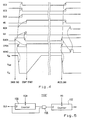
- the control circuit 112 includes four AND gates 1121 to 1124, two S-R type flip-flops (F/Fs) 1125 and 1126, a sequencer 1130, a charge-pumping circuit 1131 and a timer 1132.
- This timer 1132 includes a one-shot pulse generator 1135, an AND gate 1136 and a counter 1137.
- the AND gate 1122 responds to the write command signal WR, the address detection signal AED and a first CPU maching cycle control signal ⁇ 1 to generate the write address latch enable signal WALE.
- F/F 1125 is set by the signal WALE to inform the sequencer of the data write request from CPU 20 via a write request signal WCM.
- the AND gate 1121 responds to the signals WR and WCM and a second CPU machine cycle control signal ⁇ 2 to generates the write data latch enable signal WDLE.
- F/F 1125 is reset by a data write process end signal WEND from the sequencer 1130.
- the AND gate 1123 responds to the read command signal RD, the address detection signal AED and the first maching control signal ⁇ 1 to generate the read address latch enable signal RALE.
- F/F 1126 is set by the signal RALE to inform the sequencer 1130 of the data read request from CPU 20 via a read request signal RCM. This signal RCM is also supplied to MPX 106 as the address selection signal AS.
- the AND gate 1124 detects a data read bus cycle by the inverted signal RD and the signal ⁇ 1 and resets F/F 1126.
- the sequencer 1130 responds to the write request signal WCM, read request signal RCM and operation end signal EWEN from the timer 1132 to generate the above control signals SE, OE, WE, GCS, SCS and DCS in accordance with predetermined sequence.
- the sequence 1130 can be easily constituted of various gate circuits and/or a PLA (programmable logic array) circuit with reference to timing charts shown in Figs. 3 and 4 which will be described later.
- the sequence 1130 further generates a charge-pumping enable signal CPEN to the charge-pumping circuit 1131.
- this circuit 1131 has capacitors and transistor switches and boosts the Vcc voltage up to Vpp level in response to a boosting clock signal (not shown) and the active level of the signal CPEN.
- the inactive level of CPEN clamps the energizing voltage Vsup at Vcc level.
- the charge-pumping circuit 113 boosts Vcc voltage up to Vpp voltage
- the energizing voltage Vsup reaches Vpp level from Vcc level after a voltage raising-up time has elapsed, as shown by "T1" in Fig. 8.
- T1 voltage raising-up time
- the erasing/writing operation is terminated.
- the sum of these times T1 and T2 is a preset time T of the timer 1132.
- the timer 1132 detects the preset time T by counting a reference clock signal CLK by means of the counter 1137 and generates the operation end signal EWEN.
- the AND gate 1136 is inserted into the supply line of clock signal CLK. Accordingly, the counter 1137 counts the clock signal CLK during the open state of the gate 1136.
- the open and closed states of the gate 1136 is controlled by a one-shot pulse signal OSP from the generator 1135.
- the generator 1135 When F/F 1126 is set, i.e., when the data read request is issued, the generator 1135 changes the signal OSP to the low level during the predetermined time period to close the AND gate 1136.
- the generator 1135 may be constituted of a CR time constant circuit and an inverter.
- CPU 20 When CPU 20 executes a data write instruction to E2PROM 10, it generates the write command signal WR and transfers a write address onto the bus 70 in synchronism with the first maching cycle control signal ⁇ 1. CPU 20 thereafter transfers data to be written (write data) onto the bus 70 in synchronism with the second machine cycle control signal ⁇ 2.
- the AND gates generates the latch enable signal WALE, so that the latch circuit 102 latches the write address.
- the latch signal WDLE is generated by the AND gate 1121, the latch circuit 104 latches the write data. Since the signal AS assumes the low level, MPX 106 supplies the write address from the latch circuit 102 to the row decoder 109 and column selector 110.
- F/F 1125 is set by the signal WALE to change the write request signal WCM to the high level.
- the sequencer 1130 changes the drain control signal DCS to the low level to open drain of each of selected memory cells.
- the signals GCS and SCS are held at the high level.
- the sequencer 1130 further generates a reset pulse RS to reset the counter 1137 and changes the charge-pumping enable signal CPEN to the active, high, level.
- the counter 1137 starts to count to the clock signal CLK.
- the charge-pumping circuit 1131 starts the boosting operation.
- the energizing voltage Vsup of Vpp level is supplied to the row decoder 109, which is turn supplies Vpp level to the control gate of each selected memory cell having source grounded and drain opened. The erasing operation thus starts.
- CPU 20 after issuing the data write request to E2PROM 10, reads out each of subsequent instructions from the program memory 40 and executes it. Therefore, CPU 20 may encounter a data read instruction from E2PROM 10. When CPU 20 encounter such instruction, it generates the read command signal RD and transfers a read address onto the bus 70 in synchronism with the signal ⁇ 1. In response thereto, the AND gate 1123 generates the latch enable signal RALE, so that the read address is latched into the latch circuit 103. F/F 1126 is set by the signal RALE to change the signal AS (RCM) to the high level. MPX 106 selects the latch circuit 103 to supply the read address to the row decoder 109 and column selector 110.
- the sequencer 1130 changes the signal CPEN to the low level.
- the charge-pumping circuit 1131 is thereby deactived and the energizing voltage Vsup is clamped, at Vcc level.
- the sequence 1130 further changes the signal DCS to the high level and then changes the signal SE to the high level to activate the sense amplifier 108.
- the sequencer 1130 thereafter changes the signal OE to the high level in synchronism with ⁇ 2.
- the bus driver 105 is thereby activated, so that data stored in memory cells selected by the read address are transferred onto the bus 70.
- the generator 1135 changes the signal OSP to the low level.
- the AND gate 1136 is closed and the counter 1137 suspends to count the clock signal CLK.
- CPU 20 inverts the read command signal RD to the low level in synchronism with ⁇ 1, so that F/F 1126 is reset.
- As (RCM) signal is thereby changed to the low level.
- MPX 106 selects the latch circuit 102.
- the sequencer 1130 inverts SE, OE and DCS signals to the low level and further inverts CPEN signal to the high level. Therefore, the charge-pumping circuit 1131 starts the boosting operation and boosts the voltage Vsup up to Vpp level after the time T1.
- the OSP signal is held at the low level even after the read request signal RCM is changed to the low level.
- the charge-pumping circuit 1131 boosts the voltage Vsup up to Vpp level after T1 time has elapsed. During this time T1, the valid or substantial data erasing is not performed.
- the signal OSP is held at the low level.
- the generator 1135 changes the OSP signal to the high level. The counter 1137 thereby resumes to count the clock signal CLK. Since the voltage raising-up time T1 depends on the circuit construction of the charge-pumping circuit 1131 and since the data read bus cycle period is determined by ⁇ 1 and ⁇ 2, the low level period of OSP signal can be easily determined.
- the time count operation of the timer 1132 is also suspended during the period corresponding to the sum of the data read cycle period and the voltage raising-up time T1.
- the counter 1137 advances to count the clock signal CLK and, when the time T2 required to erase data has been elapsed, the timer 1132 generates the erasing end signal EWEN, as shown in Fig. 4.
- the sequencer 1130 produces the low level CPEN signal to clamp the voltage Vsup at Vcc level and then changes GCS, SCS and DCS signals to the low level, low level and high level, respectively.
- the sequencer 1130 produces the pulse RS to reset the counter and then changes CPEN and WE signals to the high level.
- the write circuit 107 is thereby activated. Thus, the writing operation starts.
- the counter 1137 starts to count the clock signal CLK.
- the timer 1132 When the time T has elapsed, the timer 1132 produces the writing end signal EWEN. In response thereto, the sequencer 1130 inverts CPEN signal to the low level and then changes GCS, SCS and WE signals to high level, high level and low level, respectively. The data write processing end signal WEND is thereafter generated to reset F/F 1125. Thus, the data write process responsive to the data write request is completed.
- CPU 20 issues the data read request during the writing operation, the writing operation is suspended and the data is then read out of the selected address, the suspended writing operation being thereafter resumed, similarly to Fig. 3.
- the counter 1137 also suspends the count operation during the period corresponding to the sum of the read bus cycle period and the voltage raising-up time T1.
- a time 1132′ includes a counter 1138 in place of the one-shot pulse generator 1135 shown in Fig. 2.
- This counter 1138 is reset by the high level RCM signal.
- the counter 1138 starts to count the clock pulse CLK and generates a high level overflow signal after the time T1 elapses.
- the AND gate 1136 is thereby opened.
- the high level overflow signal is held until the next high level RCM signal is applied to the counter 1138.
Abstract
Description
- The present invention relates to a microcomputer and, more particularly, to a microcomputer having an electrically erasable and programmable nonvolatile memory (called hereinafter "E²PROM") as a data memory.
- A random access memory (RAM) is generally employed as a data memory of a microcomputer, which stores data to be processed and processed resultant data. However, RAM has an unavoidable problem that data stored therein are destroyed when a power voltage supplied thereto is cut off. Therefore, E²PROM is employed as a part of that data memory to store and hold data which are required to be kept stored even after a power voltage is cut off.
- A data write process to E²PROM consists of an erasing operation, which is first performed to initialize the memory cell at an address to be written with new data by erasing the data formerly stored at that address, and a writing operation, which is subsequently performed to write the new data into that address. As well known in the art, the erasing and writing operations require a relatively long time duration, about 10 msec, respectively. This time duration is extremely long in comparison with an instruction execution time or a maching cycle time of CPU (Central Processing Unit). If CPU is programmed to perform the data write process to E²PROM, the execution efficiency of the program is deteriorated remarkably.
- In order to solve this problem, an erasing and writing automaton circuit is provided to control the data write process to E²PROM in place of CPU. When CPU receives a data write instruction to E²PROM, it issues the automaton circuit with a data write request including a write address information, data to be written (i.e., write data) and a write command signal. CPU is thereafter shifted to a subsequent operation to execute other instructions.
- On the other hand, the erasing and writing automaton circuit is initiated by the data write request to first perform the erasing operation in which a so-called Vpp voltage higher than a power voltage applied to the CPU is applied to memory cells of the selected address of E²PROM for the above-mentioned relatively long period. The data, which have been stored in those memory cells, are thereby erased. When the erasing operation is completed, the writing operation is performed to apply the Vpp voltage or ground voltage to the selected memory cells in accordance with data to be written for the relatively long period. The new data is thereby stored in the selected memory cells. In order to detect each of the erasing and writing operation time durations, the automaton circuit includes a timer for counting a reference clock signal and to generate an operation end signal when a predetermine time has elapsed. In response to this operation end signal, the application of the Vpp voltage to the selected memory cells is terminated to thereby complete the erasing and writing operations.
- Since CPU executed subsequent instructions in parallel to the data write process by the automaton circuit, there occurs a case that CPU encounters a data read instruction from E²PROM. Since that data read operation from E²PROM can be performed at a high speed, similarly to the data read operation from RAM, the data read instruction from E²PROM is executed immediately without being waited until the current data write process to E²PROM is completed. When CPU executed the data read instruction for reading out from E²PROM, it issued the automaton circuit with a data read request including read address information and a read command signal. In response to this request, the automaton circuit suspends the data write process and then brings E²PROM into a data read operation mode. An address of E²PROM selected by the read address information is accessed and data stored therein is then transferred to CPU. The suspended data write process is thereafter resumed.
- Thus, the data write process may be temporarily suspended by the data read request issued from CPU. However, the automaton circuit automatically completes the erasing and writing operations in response to the operation end signal generated by the timer. For this reason, the application time of the Vpp voltage to the selected memory cells is shortened by the suspended time of the data write process. The data is thereby not substantially written into E²PROM. This drawback can be solved by initializing or resetting the timer in response to the data read request. However, in that case, the data write process is again performed from the beginning, so that a time for preforming the data write process is prolonged undesirably.
- Therefore, an object of the present invention is to provide a microcomputer including E²PROM equipped with an improved data erasing, writing and read control circuit.
- Another object of the present invention is to provide a microcomputer having E²PROM into which data is surely written without prolonging a data write processing time.
- Still another object of the present invention is to provide an E²PROM equipped with a control circuit which performs a data write process to surely write data into selected memory cells without prolonging a processing time even when a data read request is issued during the data write processing operation.
- A microcomputer according to the present invention comprises E²PROM, CPU executing a program and issuing a data write request and a data read request to E²PROM, and a data/erasing/writing/reading control circuit including a timer counting a time to generate a processing end signal when a predetermined time has elapsed, a data write process control circuit responding to the data write request to perform a data write process in which data stored in a selected memory cell of E²PROM is first erased and new data is then written into the selected memory cell and responding to the processing end signal to terminate the data write process, a data read control circuit responding to the data read request issued during the data write process to suspend the data write process, read out data from a selected memory cell and resume the suspended data write process, and a timer control circuit suspending the time counting operation of the timer during the suspended period of the data write process.
- Thus, if the data write processed is suspended, the timer is supended to count a time, not initialized or reset. This is based upon a fact that while the Vpp voltage has to be applied to the memory cell for a preselected time in order to erase data thereof and write new data thereinto, the continuous application of the Vpp voltage over the preselected time is not required and the total application time of the Vpp voltage is required to satisfy the preselected time. For example, assuming that the preselected time is 10 msec, it is required to continuously apply the Vpp voltage for 10 msec, and the Vpp voltage can be applied five times 2 msec by 2 msec.
- As a result, even if the data write process is suspended by the data read request, the data is surely written into the selected memory cell of E²PROM without prolong the data write processing time.
- The above and other objects, advantages and features of the present invention will be more apparent from the following description taken in conjunction with the accompanying drawings, in which
- Fig. 1 is a block diagram representative of E²PROM according to an embodiment of the present invention;
- Fig. 2 is a block diagram representative of an erasing/writing/reading control circuit shown in Fig. 1;
- Figs. 3 and 4 are timing charts representative of an operation of E²PROM shown in Fig. 1;
- Fig. 5 is a block diagram representative of another embodiment of a timer shown in Fig. 2;
- Fig. 6 is block diagram representative of a microcomputer employing E²PROM shown in Fig. 1;
- Figs. 7A, 7B and 7C are equivalent circuits of one E²PROM memory cell in an erasing mode, a write mode and a reading mode, respectively; and
- Fig. 8 is a waveform diagram representative of an output voltage of a charge-pumping circuit shown in Fig. 2.
- Referring to Fig. 1, E²PROM 10 according to an embodiment of the present invention is coupled to an address/
data multiplex bus 70. - Referring to Fig. 6, the
bus 70 is in turn coupled toCPU 20. Further coupled to thebus 70 are adata memory 30 constituted of a static type RAM (SRAM), aprogram memory 40 constituted of a mask ROM, and a peripheral I/O unit 50 including an A/D converter, a serial interface unit, a timer counter and so forth, all not shown. Theunit 50 is also coupled to an I/O bus 80 to controlled devices (not shown). Therespective units 10 to 50 are further interconnected via acontrol bus 60.CPU 20 reads out each instruction from theprogram memory 40 and by executing it, performs arithmetic and/or logic operation on operand data.CPU 20 further performs data read and write operations to E²PROM 10,data memory 30 and I/O unit 50. - Turning back to Fig. 1, E²PROM 10 includes an E²PROM
address detector 101, a writeaddress latch circuit 102, a readaddress latch circuit 103, a writedata latch circuit 104 and abus driver 105 which are connected to thebus 70. Theaddress detector 101 detects whether or not the address information on thebus 70 exists in a memory space allocated to E²PROM 10 and generates a high level address detection signal AED when the address information is detected to exist in the memory space. In the present embodiment, E²PROM 10 is allocated to a memory space from "500H" to "8FFH" and thus has a memory capacity of 1 K byte. The mark "H" represents a hexiadecimal notation. Thedetector 101 decodes more significant four bits of the address information on thebus 70 and generates the high level signal AED when the content of those four bits is "5H", "6H", "7H" or "8H". Thelatch circuit 102 latches the information on thebus 70 as a write address in response to a write address latch enable signal WALE supplied thereto, and thelatch circuit 103 latches the information on the bus as a read address in response to a read address latch enable signal RALE. Thelatch circuit 104 latches the information on thebus 70 as data to be written (i.e., write data) in response to a write data latch enable signal WDLE. The output address of thelatch circuits MPX 106 selects the output address of thelatch circuit 102 when the signal AS assumes that low level and selects the output address of thelatch circuit 103 when the signal AS assumes the high level. A part of the address selected byMPX 106 is supplied to arow decoder 109 as a row address and the remaining part thereof is supplied to acolumn selector 110 as a column address. AnE²PROM cell array 111 includes a number of E²PROM memory cells arranged in rows and columns. A predetermined number of memory cells are selected by therow decoder 109 and thecolumn selector 110. In a data read operation, data stored in the selected memory cells are read out therefrom and amplified by a read-out circuit (sense amplifier) 108 responsive to a sense-enable signal SE. The read-out data are then transferred onto thebus 70 via thebus driver 105 in response to an output-enable signal OE. - In this embodiment, each of the memory cells is constituted of an insulated gate field effect transistor having a floating gate, as shown in Fig. 7. The data erasing operation of the cell is performed with source S being grounded, drain D being opened and control gate being applied with Vpp voltage, as shown in Fig. 7A. The data writing operation of the cell is performed with source being opened, control gate being grounded and drain being applied with Vpp voltage or ground voltage from a write circuit 107 (Fig. 1) in accordance with data to be written, as shown in Fig. 7B. The data reading operation of the cell is performed with source being grounded and control gate being applied with a read-out voltage VRD, and drain is coupled to the
sense amplifier 108 via thecolumn selector 110. Thus, in response to the respective operations, the voltage states of source, drain and control gate of the selected memory cell are controlled. - Turning back again to Fig. 1, the E²PROM cell array 11 is supplied with a source control signal SCS and a drain control signal DCS. The high level of the signal SCS grounds source of the selected memory cell and the low level thereof opens it. The high level of the signal DCS coupled to drain of the selected memory cell to the
sense amplifier 108 and thewrite circuit 107 via thecolumn selector 110 and the low level thereof opens it. Thewrite circuit 107 is activated by a write-enable signal WE and then applies Vpp voltage or ground voltage to drain of the selected memory cell in accordance with the data to be written from thelatch circuit 104. A gate control signal GCS is supplied to therow decoder 109 which further receives an energizing voltage Vsup taking Vpp level in the erasing and writing operation and taking a power voltage level Vcc in the read operation, the power voltage Vcc being applied toE²PROM 10. When the signal GCS assumes the high level, therow decoder 109 applies Vpp voltage to control gate of the selected memory in the erasing operation and supplies the read-out voltage VRD thereto in the reading operation. On the other hand, the low level of the signal GCS grounds the control gate of the selected memory cell. The energizing voltage Vsup is further supplied to thecolumn selector 110. The above-mentioned control signals and energizing voltage are generated by a data erasing/writing/reading control circuit 112. Thiscircuit 112 operates in predetermined sequence in response to the signal AED from theaddress detector 101 and write and read command signals WR and RD supplied via thecontrol bus 60 fromCPU 20. - Referring to Fig. 2, the
control circuit 112 includes four ANDgates 1121 to 1124, two S-R type flip-flops (F/Fs) 1125 and 1126, asequencer 1130, a charge-pumping circuit 1131 and atimer 1132. Thistimer 1132 includes a one-shot pulse generator 1135, an ANDgate 1136 and acounter 1137. The ANDgate 1122 responds to the write command signal WR, the address detection signal AED and a first CPU maching cycle control signal φ1 to generate the write address latch enable signal WALE. F/F 1125 is set by the signal WALE to inform the sequencer of the data write request fromCPU 20 via a write request signal WCM. The ANDgate 1121 responds to the signals WR and WCM and a second CPU machine cycle control signal φ2 to generates the write data latch enable signal WDLE. F/F 1125 is reset by a data write process end signal WEND from thesequencer 1130. The ANDgate 1123 responds to the read command signal RD, the address detection signal AED and the first maching control signal φ1 to generate the read address latch enable signal RALE. F/F 1126 is set by the signal RALE to inform thesequencer 1130 of the data read request fromCPU 20 via a read request signal RCM. This signal RCM is also supplied toMPX 106 as the address selection signal AS. The ANDgate 1124 detects a data read bus cycle by the inverted signalRD and the signal φ1 and resets F/F 1126. Thesequencer 1130 responds to the write request signal WCM, read request signal RCM and operation end signal EWEN from thetimer 1132 to generate the above control signals SE, OE, WE, GCS, SCS and DCS in accordance with predetermined sequence. Thesequence 1130 can be easily constituted of various gate circuits and/or a PLA (programmable logic array) circuit with reference to timing charts shown in Figs. 3 and 4 which will be described later. Thesequence 1130 further generates a charge-pumping enable signal CPEN to the charge-pumping circuit 1131. As well known in the art, thiscircuit 1131 has capacitors and transistor switches and boosts the Vcc voltage up to Vpp level in response to a boosting clock signal (not shown) and the active level of the signal CPEN. The inactive level of CPEN clamps the energizing voltage Vsup at Vcc level. Thus, since the charge-pumping circuit 113 boosts Vcc voltage up to Vpp voltage, the energizing voltage Vsup reaches Vpp level from Vcc level after a voltage raising-up time has elapsed, as shown by "T₁" in Fig. 8. When the voltage Vsup reaches Vpp level, the valid or substantial erasing/writing operation starts. After Vpp level is applied to the selected memory cell during a time T₂ shown in Fig. 8, the erasing/writing operation is terminated. The sum of these times T₁ and T₂ is a preset time T of thetimer 1132. Thetimer 1132 detects the preset time T by counting a reference clock signal CLK by means of thecounter 1137 and generates the operation end signal EWEN. The ANDgate 1136 is inserted into the supply line of clock signal CLK. Accordingly, thecounter 1137 counts the clock signal CLK during the open state of thegate 1136. The open and closed states of thegate 1136 is controlled by a one-shot pulse signal OSP from thegenerator 1135. When F/F 1126 is set, i.e., when the data read request is issued, thegenerator 1135 changes the signal OSP to the low level during the predetermined time period to close the ANDgate 1136. Thegenerator 1135 may be constituted of a CR time constant circuit and an inverter. - An operation will described below with reference also to Figs. 3 and 4.
- When
CPU 20 executes a data write instruction to E²PROM 10, it generates the write command signal WR and transfers a write address onto thebus 70 in synchronism with the first maching cycle control signal φ1.CPU 20 thereafter transfers data to be written (write data) onto thebus 70 in synchronism with the second machine cycle control signal φ2. In response thereto, the AND gates generates the latch enable signal WALE, so that thelatch circuit 102 latches the write address. Further, since the latch signal WDLE is generated by the ANDgate 1121, thelatch circuit 104 latches the write data. Since the signal AS assumes the low level,MPX 106 supplies the write address from thelatch circuit 102 to therow decoder 109 andcolumn selector 110. F/F 1125 is set by the signal WALE to change the write request signal WCM to the high level. In response thereto, thesequencer 1130 changes the drain control signal DCS to the low level to open drain of each of selected memory cells. The signals GCS and SCS are held at the high level. Thesequencer 1130 further generates a reset pulse RS to reset thecounter 1137 and changes the charge-pumping enable signal CPEN to the active, high, level. Thecounter 1137 starts to count to the clock signal CLK. The charge-pumping circuit 1131 starts the boosting operation. After the time T₁ is elapsed, the energizing voltage Vsup of Vpp level is supplied to therow decoder 109, which is turn supplies Vpp level to the control gate of each selected memory cell having source grounded and drain opened. The erasing operation thus starts. - On the other hand,
CPU 20, after issuing the data write request to E²PROM 10, reads out each of subsequent instructions from theprogram memory 40 and executes it. Therefore,CPU 20 may encounter a data read instruction fromE²PROM 10. WhenCPU 20 encounter such instruction, it generates the read command signal RD and transfers a read address onto thebus 70 in synchronism with the signal φ1. In response thereto, the ANDgate 1123 generates the latch enable signal RALE, so that the read address is latched into thelatch circuit 103. F/F 1126 is set by the signal RALE to change the signal AS (RCM) to the high level.MPX 106 selects thelatch circuit 103 to supply the read address to therow decoder 109 andcolumn selector 110. In response to the high level read request signal RCM, thesequencer 1130 changes the signal CPEN to the low level. The charge-pumping circuit 1131 is thereby deactived and the energizing voltage Vsup is clamped, at Vcc level. Thesequence 1130 further changes the signal DCS to the high level and then changes the signal SE to the high level to activate thesense amplifier 108. Thesequencer 1130 thereafter changes the signal OE to the high level in synchronism with φ2. Thebus driver 105 is thereby activated, so that data stored in memory cells selected by the read address are transferred onto thebus 70. In response to the high level read request signal RCM, thegenerator 1135 changes the signal OSP to the low level. As a result, the ANDgate 1136 is closed and thecounter 1137 suspends to count the clock signal CLK. -
CPU 20 inverts the read command signal RD to the low level in synchronism with φ1, so that F/F 1126 is reset. As (RCM) signal is thereby changed to the low level. In response to low level AS signal,MPX 106 selects thelatch circuit 102. In response to low level PCM signal, thesequencer 1130 inverts SE, OE and DCS signals to the low level and further inverts CPEN signal to the high level. Therefore, the charge-pumping circuit 1131 starts the boosting operation and boosts the voltage Vsup up to Vpp level after the time T₁. - It should be noted that the OSP signal is held at the low level even after the read request signal RCM is changed to the low level. As described above, the charge-
pumping circuit 1131 boosts the voltage Vsup up to Vpp level after T₁ time has elapsed. During this time T₁, the valid or substantial data erasing is not performed. In order to prevent thecounter 1137 from advancing the count value thereof, the signal OSP is held at the low level. At a time point corresponding to a timing at which the voltage Vsup reaches Vpp level, thegenerator 1135 changes the OSP signal to the high level. Thecounter 1137 thereby resumes to count the clock signal CLK. Since the voltage raising-up time T₁ depends on the circuit construction of the charge-pumping circuit 1131 and since the data read bus cycle period is determined by φ1 and φ2, the low level period of OSP signal can be easily determined. - Thus, if the data write process is suspended by the data read request, the time count operation of the
timer 1132 is also suspended during the period corresponding to the sum of the data read cycle period and the voltage raising-up time T₁. - The
counter 1137 advances to count the clock signal CLK and, when the time T₂ required to erase data has been elapsed, thetimer 1132 generates the erasing end signal EWEN, as shown in Fig. 4. In response thereto, thesequencer 1130 produces the low level CPEN signal to clamp the voltage Vsup at Vcc level and then changes GCS, SCS and DCS signals to the low level, low level and high level, respectively. Thereafter, thesequencer 1130 produces the pulse RS to reset the counter and then changes CPEN and WE signals to the high level. Thewrite circuit 107 is thereby activated. Thus, the writing operation starts. Thecounter 1137 starts to count the clock signal CLK. - When the time T has elapsed, the
timer 1132 produces the writing end signal EWEN. In response thereto, thesequencer 1130 inverts CPEN signal to the low level and then changes GCS, SCS and WE signals to high level, high level and low level, respectively. The data write processing end signal WEND is thereafter generated to reset F/F 1125. Thus, the data write process responsive to the data write request is completed. WhenCPU 20 issues the data read request during the writing operation, the writing operation is suspended and the data is then read out of the selected address, the suspended writing operation being thereafter resumed, similarly to Fig. 3. At this time, thecounter 1137 also suspends the count operation during the period corresponding to the sum of the read bus cycle period and the voltage raising-up time T₁. - Referring to Fig. 5, a
time 1132′ according to another embodiment includes acounter 1138 in place of the one-shot pulse generator 1135 shown in Fig. 2. Thiscounter 1138 is reset by the high level RCM signal. In response to the change of RCM signal to the low level, thecounter 1138 starts to count the clock pulse CLK and generates a high level overflow signal after the time T₁ elapses. The ANDgate 1136 is thereby opened. The high level overflow signal is held until the next high level RCM signal is applied to thecounter 1138. - The present invention is not limited to the above embodiments, but may be changed and modified without departing from the scope and spirit of the invention.
Claims (3)
Applications Claiming Priority (2)
| Application Number | Priority Date | Filing Date | Title |
|---|---|---|---|
| JP33171388 | 1988-12-27 | ||
| JP331713/88 | 1988-12-27 |
Publications (3)
| Publication Number | Publication Date |
|---|---|
| EP0376285A2 true EP0376285A2 (en) | 1990-07-04 |
| EP0376285A3 EP0376285A3 (en) | 1990-09-05 |
| EP0376285B1 EP0376285B1 (en) | 1994-03-09 |
Family
ID=18246757
Family Applications (1)
| Application Number | Title | Priority Date | Filing Date |
|---|---|---|---|
| EP89124030A Expired - Lifetime EP0376285B1 (en) | 1988-12-27 | 1989-12-27 | Microcomputer having electrically erasable and programmable nonvolatile memory |
Country Status (3)
| Country | Link |
|---|---|
| US (1) | US5287469A (en) |
| EP (1) | EP0376285B1 (en) |
| DE (1) | DE68913695T2 (en) |
Cited By (36)
| Publication number | Priority date | Publication date | Assignee | Title |
|---|---|---|---|---|
| US5214605A (en) * | 1990-08-20 | 1993-05-25 | Samsung Electronics Co., Ltd. | Automatic erasing optimization circuit for an electrically erasable and programmable semiconductor memory and method thereof |
| EP0587445A2 (en) * | 1992-09-11 | 1994-03-16 | Mitsubishi Denki Kabushiki Kaisha | Semiconductor integrated circuit and IC card using the same |
| EP0598974A2 (en) * | 1992-11-24 | 1994-06-01 | Mitsubishi Denki Kabushiki Kaisha | Semiconductor integrated circuit |
| EP0662691A1 (en) * | 1993-12-28 | 1995-07-12 | STMicroelectronics S.r.l. | Count unit for non volatile memories |
| EP0833250A1 (en) * | 1996-09-30 | 1998-04-01 | Nokia Mobile Phones Ltd. | Memory device |
| WO1998039773A1 (en) * | 1997-03-05 | 1998-09-11 | Advanced Micro Devices, Inc. | Non-volatile memory enabling simultaneous reading and writing by time multiplexing a decode path |
| US5847998A (en) * | 1996-12-20 | 1998-12-08 | Advanced Micro Devices, Inc. | Non-volatile memory array that enables simultaneous read and write operations |
| US5867430A (en) * | 1996-12-20 | 1999-02-02 | Advanced Micro Devices Inc | Bank architecture for a non-volatile memory enabling simultaneous reading and writing |
| EP0900440A1 (en) * | 1996-05-22 | 1999-03-10 | Macronix International Co., Ltd. | Flash memory device with multiple checkpoint erase suspend logic |
| EP0931289A4 (en) * | 1996-09-20 | 2000-10-04 | Intel Corp | Nonvolatile writeable memory with program suspend command |
| FR2798769A1 (en) * | 1999-09-20 | 2001-03-23 | St Microelectronics Sa | Circuit for programming or deleting data on a memory cell, comprises voltage generation and selection circuits and control unit with timing circuits to fix programming/deletion time to preset value |
| US7053034B2 (en) | 2002-04-10 | 2006-05-30 | Salvona, Llc | Targeted controlled delivery compositions activated by changes in pH or salt concentration |
| EP2966573A1 (en) * | 2014-07-08 | 2016-01-13 | Adesto Technologies Corporation | Concurrent read and write operations in a serial flash device |
| WO2016014249A1 (en) * | 2014-07-22 | 2016-01-28 | Sandisk Enterprise Ip Llc | Suspending and resuming non-volatile memory operations |
| US20160070473A1 (en) * | 2014-09-08 | 2016-03-10 | Apple Inc. | Method to enhance programming performance in multilevel nvm devices |
| US9436397B2 (en) | 2014-09-23 | 2016-09-06 | Sandisk Technologies Llc. | Validating the status of memory operations |
| US9558125B2 (en) | 2014-10-27 | 2017-01-31 | Sandisk Technologies Llc | Processing of un-map commands to enhance performance and endurance of a storage device |
| US9647697B2 (en) | 2015-03-16 | 2017-05-09 | Sandisk Technologies Llc | Method and system for determining soft information offsets |
| US9645765B2 (en) | 2015-04-09 | 2017-05-09 | Sandisk Technologies Llc | Reading and writing data at multiple, individual non-volatile memory portions in response to data transfer sent to single relative memory address |
| US9652415B2 (en) | 2014-07-09 | 2017-05-16 | Sandisk Technologies Llc | Atomic non-volatile memory data transfer |
| US9715939B2 (en) | 2015-08-10 | 2017-07-25 | Sandisk Technologies Llc | Low read data storage management |
| US9753653B2 (en) | 2015-04-14 | 2017-09-05 | Sandisk Technologies Llc | High-priority NAND operations management |
| US9753649B2 (en) | 2014-10-27 | 2017-09-05 | Sandisk Technologies Llc | Tracking intermix of writes and un-map commands across power cycles |
| US9778878B2 (en) | 2015-04-22 | 2017-10-03 | Sandisk Technologies Llc | Method and system for limiting write command execution |
| US9817752B2 (en) | 2014-11-21 | 2017-11-14 | Sandisk Technologies Llc | Data integrity enhancement to protect against returning old versions of data |
| US9824007B2 (en) | 2014-11-21 | 2017-11-21 | Sandisk Technologies Llc | Data integrity enhancement to protect against returning old versions of data |
| US9837146B2 (en) | 2016-01-08 | 2017-12-05 | Sandisk Technologies Llc | Memory system temperature management |
| US9864545B2 (en) | 2015-04-14 | 2018-01-09 | Sandisk Technologies Llc | Open erase block read automation |
| US9870149B2 (en) | 2015-07-08 | 2018-01-16 | Sandisk Technologies Llc | Scheduling operations in non-volatile memory devices using preference values |
| US9904621B2 (en) | 2014-07-15 | 2018-02-27 | Sandisk Technologies Llc | Methods and systems for flash buffer sizing |
| US9952978B2 (en) | 2014-10-27 | 2018-04-24 | Sandisk Technologies, Llc | Method for improving mixed random performance in low queue depth workloads |
| US10126970B2 (en) | 2015-12-11 | 2018-11-13 | Sandisk Technologies Llc | Paired metablocks in non-volatile storage device |
| US10228990B2 (en) | 2015-11-12 | 2019-03-12 | Sandisk Technologies Llc | Variable-term error metrics adjustment |
| US10372529B2 (en) | 2015-04-20 | 2019-08-06 | Sandisk Technologies Llc | Iterative soft information correction and decoding |
| US10481830B2 (en) | 2016-07-25 | 2019-11-19 | Sandisk Technologies Llc | Selectively throttling host reads for read disturbs in non-volatile memory system |
| US10732856B2 (en) | 2016-03-03 | 2020-08-04 | Sandisk Technologies Llc | Erase health metric to rank memory portions |
Families Citing this family (94)
| Publication number | Priority date | Publication date | Assignee | Title |
|---|---|---|---|---|
| JP3152535B2 (en) * | 1993-03-18 | 2001-04-03 | 富士通株式会社 | Data processing device |
| FR2711831B1 (en) * | 1993-10-26 | 1997-09-26 | Intel Corp | Method and circuit for storing and prioritizing erasure orders in a memory device. |
| US5559988A (en) * | 1993-12-30 | 1996-09-24 | Intel Corporation | Method and circuitry for queuing snooping, prioritizing and suspending commands |
| FR2732151B1 (en) * | 1995-03-21 | 1997-04-25 | Sgs Thomson Microelectronics | WRITE PROTECTION METHOD FOR A MEMORY IN AN INTEGRATED CIRCUIT AND CORRESPONDING INTEGRATED CIRCUIT |
| US5742787A (en) * | 1995-04-10 | 1998-04-21 | Intel Corporation | Hardware reset of a write state machine for flash memory |
| US5790813A (en) * | 1996-01-05 | 1998-08-04 | Unisys Corporation | Pre-arbitration system allowing look-around and bypass for significant operations |
| US5940861A (en) * | 1996-09-20 | 1999-08-17 | Intel Corporation | Method and apparatus for preempting operations in a nonvolatile memory in order to read code from the nonvolatile memory |
| US6201739B1 (en) | 1996-09-20 | 2001-03-13 | Intel Corporation | Nonvolatile writeable memory with preemption pin |
| US6189070B1 (en) * | 1997-08-28 | 2001-02-13 | Intel Corporation | Apparatus and method for suspending operation to read code in a nonvolatile writable semiconductor memory |
| JPH11203266A (en) * | 1998-01-07 | 1999-07-30 | Mitsubishi Electric Corp | Microcomputer |
| US6226728B1 (en) | 1998-04-21 | 2001-05-01 | Intel Corporation | Dynamic allocation for efficient management of variable sized data within a nonvolatile memory |
| US6930925B2 (en) * | 2003-10-14 | 2005-08-16 | Atmel Corporation | Suspend-resume programming method for flash memory |
| JP4510498B2 (en) * | 2004-04-05 | 2010-07-21 | セイコーインスツル株式会社 | Semiconductor integrated circuit |
| US7962576B2 (en) * | 2004-07-22 | 2011-06-14 | Sap Ag | Quantity conversion interface for external program calls |
| US20060053247A1 (en) * | 2004-09-08 | 2006-03-09 | Hugo Cheung | Incremental erasing of flash memory to improve system performance |
| EP1835508B1 (en) | 2006-03-16 | 2012-01-18 | Samsung Electronics Co., Ltd. | Pram and associated operation method and system |
| KR100816748B1 (en) * | 2006-03-16 | 2008-03-27 | 삼성전자주식회사 | Phase change memory device supporting program suspend/resume mode and program method thereof |
| WO2007132457A2 (en) | 2006-05-12 | 2007-11-22 | Anobit Technologies Ltd. | Combined distortion estimation and error correction coding for memory devices |
| WO2007132456A2 (en) | 2006-05-12 | 2007-11-22 | Anobit Technologies Ltd. | Memory device with adaptive capacity |
| WO2007132453A2 (en) | 2006-05-12 | 2007-11-22 | Anobit Technologies Ltd. | Distortion estimation and cancellation in memory devices |
| US8060806B2 (en) * | 2006-08-27 | 2011-11-15 | Anobit Technologies Ltd. | Estimation of non-linear distortion in memory devices |
| WO2008053472A2 (en) * | 2006-10-30 | 2008-05-08 | Anobit Technologies Ltd. | Reading memory cells using multiple thresholds |
| US7924648B2 (en) * | 2006-11-28 | 2011-04-12 | Anobit Technologies Ltd. | Memory power and performance management |
| WO2008068747A2 (en) | 2006-12-03 | 2008-06-12 | Anobit Technologies Ltd. | Automatic defect management in memory devices |
| US7900102B2 (en) | 2006-12-17 | 2011-03-01 | Anobit Technologies Ltd. | High-speed programming of memory devices |
| US7751240B2 (en) * | 2007-01-24 | 2010-07-06 | Anobit Technologies Ltd. | Memory device with negative thresholds |
| US8151166B2 (en) | 2007-01-24 | 2012-04-03 | Anobit Technologies Ltd. | Reduction of back pattern dependency effects in memory devices |
| WO2008111058A2 (en) | 2007-03-12 | 2008-09-18 | Anobit Technologies Ltd. | Adaptive estimation of memory cell read thresholds |
| US8001320B2 (en) | 2007-04-22 | 2011-08-16 | Anobit Technologies Ltd. | Command interface for memory devices |
| US8234545B2 (en) | 2007-05-12 | 2012-07-31 | Apple Inc. | Data storage with incremental redundancy |
| US8429493B2 (en) * | 2007-05-12 | 2013-04-23 | Apple Inc. | Memory device with internal signap processing unit |
| US7925936B1 (en) | 2007-07-13 | 2011-04-12 | Anobit Technologies Ltd. | Memory device with non-uniform programming levels |
| US8259497B2 (en) * | 2007-08-06 | 2012-09-04 | Apple Inc. | Programming schemes for multi-level analog memory cells |
| US8174905B2 (en) | 2007-09-19 | 2012-05-08 | Anobit Technologies Ltd. | Programming orders for reducing distortion in arrays of multi-level analog memory cells |
| WO2009050703A2 (en) | 2007-10-19 | 2009-04-23 | Anobit Technologies | Data storage in analog memory cell arrays having erase failures |
| US8068360B2 (en) | 2007-10-19 | 2011-11-29 | Anobit Technologies Ltd. | Reading analog memory cells using built-in multi-threshold commands |
| US8000141B1 (en) | 2007-10-19 | 2011-08-16 | Anobit Technologies Ltd. | Compensation for voltage drifts in analog memory cells |
| WO2009063450A2 (en) | 2007-11-13 | 2009-05-22 | Anobit Technologies | Optimized selection of memory units in multi-unit memory devices |
| US8225181B2 (en) * | 2007-11-30 | 2012-07-17 | Apple Inc. | Efficient re-read operations from memory devices |
| US8209588B2 (en) | 2007-12-12 | 2012-06-26 | Anobit Technologies Ltd. | Efficient interference cancellation in analog memory cell arrays |
| KR101339288B1 (en) * | 2007-12-14 | 2013-12-09 | 삼성전자 주식회사 | Nonvolatile memory device using variable resistive element |
| US8964488B2 (en) | 2007-12-14 | 2015-02-24 | Samsung Electronics Co., Ltd. | Non-volatile memory device using variable resistance element with an improved write performance |
| US8456905B2 (en) * | 2007-12-16 | 2013-06-04 | Apple Inc. | Efficient data storage in multi-plane memory devices |
| US8085586B2 (en) | 2007-12-27 | 2011-12-27 | Anobit Technologies Ltd. | Wear level estimation in analog memory cells |
| US8156398B2 (en) | 2008-02-05 | 2012-04-10 | Anobit Technologies Ltd. | Parameter estimation based on error correction code parity check equations |
| US7924587B2 (en) | 2008-02-21 | 2011-04-12 | Anobit Technologies Ltd. | Programming of analog memory cells using a single programming pulse per state transition |
| US8230300B2 (en) | 2008-03-07 | 2012-07-24 | Apple Inc. | Efficient readout from analog memory cells using data compression |
| US8059457B2 (en) | 2008-03-18 | 2011-11-15 | Anobit Technologies Ltd. | Memory device with multiple-accuracy read commands |
| US8400858B2 (en) | 2008-03-18 | 2013-03-19 | Apple Inc. | Memory device with reduced sense time readout |
| US7924613B1 (en) | 2008-08-05 | 2011-04-12 | Anobit Technologies Ltd. | Data storage in analog memory cells with protection against programming interruption |
| US7995388B1 (en) | 2008-08-05 | 2011-08-09 | Anobit Technologies Ltd. | Data storage using modified voltages |
| US8169825B1 (en) | 2008-09-02 | 2012-05-01 | Anobit Technologies Ltd. | Reliable data storage in analog memory cells subjected to long retention periods |
| US8949684B1 (en) | 2008-09-02 | 2015-02-03 | Apple Inc. | Segmented data storage |
| US8000135B1 (en) | 2008-09-14 | 2011-08-16 | Anobit Technologies Ltd. | Estimation of memory cell read thresholds by sampling inside programming level distribution intervals |
| US8482978B1 (en) | 2008-09-14 | 2013-07-09 | Apple Inc. | Estimation of memory cell read thresholds by sampling inside programming level distribution intervals |
| US8239734B1 (en) | 2008-10-15 | 2012-08-07 | Apple Inc. | Efficient data storage in storage device arrays |
| US8261159B1 (en) | 2008-10-30 | 2012-09-04 | Apple, Inc. | Data scrambling schemes for memory devices |
| US8208304B2 (en) | 2008-11-16 | 2012-06-26 | Anobit Technologies Ltd. | Storage at M bits/cell density in N bits/cell analog memory cell devices, M>N |
| US8248831B2 (en) | 2008-12-31 | 2012-08-21 | Apple Inc. | Rejuvenation of analog memory cells |
| US8397131B1 (en) | 2008-12-31 | 2013-03-12 | Apple Inc. | Efficient readout schemes for analog memory cell devices |
| US8924661B1 (en) | 2009-01-18 | 2014-12-30 | Apple Inc. | Memory system including a controller and processors associated with memory devices |
| US8228701B2 (en) * | 2009-03-01 | 2012-07-24 | Apple Inc. | Selective activation of programming schemes in analog memory cell arrays |
| US8250328B2 (en) * | 2009-03-24 | 2012-08-21 | Micron Technology, Inc. | Apparatus and method for buffered write commands in a memory |
| US8259506B1 (en) | 2009-03-25 | 2012-09-04 | Apple Inc. | Database of memory read thresholds |
| US8832354B2 (en) | 2009-03-25 | 2014-09-09 | Apple Inc. | Use of host system resources by memory controller |
| US8238157B1 (en) | 2009-04-12 | 2012-08-07 | Apple Inc. | Selective re-programming of analog memory cells |
| US8479080B1 (en) | 2009-07-12 | 2013-07-02 | Apple Inc. | Adaptive over-provisioning in memory systems |
| US8004884B2 (en) | 2009-07-31 | 2011-08-23 | International Business Machines Corporation | Iterative write pausing techniques to improve read latency of memory systems |
| US8495465B1 (en) | 2009-10-15 | 2013-07-23 | Apple Inc. | Error correction coding over multiple memory pages |
| US8677054B1 (en) | 2009-12-16 | 2014-03-18 | Apple Inc. | Memory management schemes for non-volatile memory devices |
| US8694814B1 (en) | 2010-01-10 | 2014-04-08 | Apple Inc. | Reuse of host hibernation storage space by memory controller |
| US8677203B1 (en) | 2010-01-11 | 2014-03-18 | Apple Inc. | Redundant data storage schemes for multi-die memory systems |
| US8694853B1 (en) | 2010-05-04 | 2014-04-08 | Apple Inc. | Read commands for reading interfering memory cells |
| US8572423B1 (en) | 2010-06-22 | 2013-10-29 | Apple Inc. | Reducing peak current in memory systems |
| US8595591B1 (en) | 2010-07-11 | 2013-11-26 | Apple Inc. | Interference-aware assignment of programming levels in analog memory cells |
| US9104580B1 (en) | 2010-07-27 | 2015-08-11 | Apple Inc. | Cache memory for hybrid disk drives |
| US8645794B1 (en) | 2010-07-31 | 2014-02-04 | Apple Inc. | Data storage in analog memory cells using a non-integer number of bits per cell |
| US8856475B1 (en) | 2010-08-01 | 2014-10-07 | Apple Inc. | Efficient selection of memory blocks for compaction |
| US8493781B1 (en) | 2010-08-12 | 2013-07-23 | Apple Inc. | Interference mitigation using individual word line erasure operations |
| US8694854B1 (en) | 2010-08-17 | 2014-04-08 | Apple Inc. | Read threshold setting based on soft readout statistics |
| US9021181B1 (en) | 2010-09-27 | 2015-04-28 | Apple Inc. | Memory management for unifying memory cell conditions by using maximum time intervals |
| US8374040B2 (en) | 2011-02-25 | 2013-02-12 | International Business Machines Corporation | Write bandwidth in a memory characterized by a variable write time |
| US9754648B2 (en) | 2012-10-26 | 2017-09-05 | Micron Technology, Inc. | Apparatuses and methods for memory operations having variable latencies |
| US9740485B2 (en) | 2012-10-26 | 2017-08-22 | Micron Technology, Inc. | Apparatuses and methods for memory operations having variable latencies |
| US9734097B2 (en) | 2013-03-15 | 2017-08-15 | Micron Technology, Inc. | Apparatuses and methods for variable latency memory operations |
| JP2014186787A (en) * | 2013-03-25 | 2014-10-02 | Toshiba Corp | Nonvolatile semiconductor memory device, memory controller, and memory system |
| US9727493B2 (en) | 2013-08-14 | 2017-08-08 | Micron Technology, Inc. | Apparatuses and methods for providing data to a configurable storage area |
| US9563565B2 (en) | 2013-08-14 | 2017-02-07 | Micron Technology, Inc. | Apparatuses and methods for providing data from a buffer |
| US10365835B2 (en) | 2014-05-28 | 2019-07-30 | Micron Technology, Inc. | Apparatuses and methods for performing write count threshold wear leveling operations |
| CN111863095B (en) * | 2019-04-29 | 2022-07-29 | 北京兆易创新科技股份有限公司 | Method and device for erasing NOR flash memory |
| US11061578B2 (en) * | 2019-08-05 | 2021-07-13 | Micron Technology, Inc. | Monitoring flash memory erase progress using erase credits |
| US11556416B2 (en) | 2021-05-05 | 2023-01-17 | Apple Inc. | Controlling memory readout reliability and throughput by adjusting distance between read thresholds |
| US11847342B2 (en) | 2021-07-28 | 2023-12-19 | Apple Inc. | Efficient transfer of hard data and confidence levels in reading a nonvolatile memory |
| US20230251795A1 (en) * | 2022-02-10 | 2023-08-10 | Stmicroelectronics S.R.L. | Data memory access collision manager, device and method |
Citations (2)
| Publication number | Priority date | Publication date | Assignee | Title |
|---|---|---|---|---|
| EP0092976A2 (en) * | 1982-04-22 | 1983-11-02 | Fanuc Ltd. | Memory writing control apparatus |
| EP0270410A1 (en) * | 1986-11-04 | 1988-06-08 | STMicroelectronics S.A. | Integrated circuit of the logic type with an EPROM |
Family Cites Families (3)
| Publication number | Priority date | Publication date | Assignee | Title |
|---|---|---|---|---|
| US3961312A (en) * | 1974-07-15 | 1976-06-01 | International Business Machines Corporation | Cycle interleaving during burst mode operation |
| US4077060A (en) * | 1976-12-27 | 1978-02-28 | International Business Machines Corporation | Asymmetrical multiprocessor system |
| US4479179A (en) * | 1979-07-30 | 1984-10-23 | International Business Machines Corporation | Synchronous cycle steal mechanism for transferring data between a processor storage unit and a separate data handling unit |
-
1989
- 1989-12-27 DE DE68913695T patent/DE68913695T2/en not_active Expired - Lifetime
- 1989-12-27 EP EP89124030A patent/EP0376285B1/en not_active Expired - Lifetime
- 1989-12-27 US US07/457,245 patent/US5287469A/en not_active Expired - Fee Related
Patent Citations (2)
| Publication number | Priority date | Publication date | Assignee | Title |
|---|---|---|---|---|
| EP0092976A2 (en) * | 1982-04-22 | 1983-11-02 | Fanuc Ltd. | Memory writing control apparatus |
| EP0270410A1 (en) * | 1986-11-04 | 1988-06-08 | STMicroelectronics S.A. | Integrated circuit of the logic type with an EPROM |
Cited By (51)
| Publication number | Priority date | Publication date | Assignee | Title |
|---|---|---|---|---|
| US5214605A (en) * | 1990-08-20 | 1993-05-25 | Samsung Electronics Co., Ltd. | Automatic erasing optimization circuit for an electrically erasable and programmable semiconductor memory and method thereof |
| EP0587445A2 (en) * | 1992-09-11 | 1994-03-16 | Mitsubishi Denki Kabushiki Kaisha | Semiconductor integrated circuit and IC card using the same |
| EP0587445A3 (en) * | 1992-09-11 | 1994-11-09 | Mitsubishi Electric Corp | Semiconductor integrated circuit and IC card using the same. |
| US5517460A (en) * | 1992-09-11 | 1996-05-14 | Mitsubishi Denki Kabushiki Kaisha | Semiconductor integrated circuit and IC card using the same |
| EP0598974A2 (en) * | 1992-11-24 | 1994-06-01 | Mitsubishi Denki Kabushiki Kaisha | Semiconductor integrated circuit |
| EP0598974A3 (en) * | 1992-11-24 | 1994-11-09 | Mitsubishi Electric Corp | Semiconductor integrated circuit. |
| EP0662691A1 (en) * | 1993-12-28 | 1995-07-12 | STMicroelectronics S.r.l. | Count unit for non volatile memories |
| US5687135A (en) * | 1993-12-28 | 1997-11-11 | Sgs-Thomson Microelectronics S.R.L. | Count unit for nonvolatile memories |
| EP0900440A1 (en) * | 1996-05-22 | 1999-03-10 | Macronix International Co., Ltd. | Flash memory device with multiple checkpoint erase suspend logic |
| EP0900440A4 (en) * | 1996-05-22 | 1999-04-07 | ||
| EP0931289A4 (en) * | 1996-09-20 | 2000-10-04 | Intel Corp | Nonvolatile writeable memory with program suspend command |
| GB2317721B (en) * | 1996-09-30 | 2001-09-12 | Nokia Mobile Phones Ltd | Memory device |
| US5912848A (en) * | 1996-09-30 | 1999-06-15 | Nokia Mobile Phones Limited | Methods and apparatus for efficiently managing flash memory |
| EP0833250A1 (en) * | 1996-09-30 | 1998-04-01 | Nokia Mobile Phones Ltd. | Memory device |
| EP1209570A2 (en) * | 1996-09-30 | 2002-05-29 | Nokia Corporation | Memory device |
| EP1209570A3 (en) * | 1996-09-30 | 2006-01-04 | Nokia Corporation | Memory device |
| US5867430A (en) * | 1996-12-20 | 1999-02-02 | Advanced Micro Devices Inc | Bank architecture for a non-volatile memory enabling simultaneous reading and writing |
| US5847998A (en) * | 1996-12-20 | 1998-12-08 | Advanced Micro Devices, Inc. | Non-volatile memory array that enables simultaneous read and write operations |
| US5841696A (en) * | 1997-03-05 | 1998-11-24 | Advanced Micro Devices, Inc. | Non-volatile memory enabling simultaneous reading and writing by time multiplexing a decode path |
| WO1998039773A1 (en) * | 1997-03-05 | 1998-09-11 | Advanced Micro Devices, Inc. | Non-volatile memory enabling simultaneous reading and writing by time multiplexing a decode path |
| FR2798769A1 (en) * | 1999-09-20 | 2001-03-23 | St Microelectronics Sa | Circuit for programming or deleting data on a memory cell, comprises voltage generation and selection circuits and control unit with timing circuits to fix programming/deletion time to preset value |
| US7053034B2 (en) | 2002-04-10 | 2006-05-30 | Salvona, Llc | Targeted controlled delivery compositions activated by changes in pH or salt concentration |
| EP2966573A1 (en) * | 2014-07-08 | 2016-01-13 | Adesto Technologies Corporation | Concurrent read and write operations in a serial flash device |
| US9652415B2 (en) | 2014-07-09 | 2017-05-16 | Sandisk Technologies Llc | Atomic non-volatile memory data transfer |
| US9904621B2 (en) | 2014-07-15 | 2018-02-27 | Sandisk Technologies Llc | Methods and systems for flash buffer sizing |
| WO2016014249A1 (en) * | 2014-07-22 | 2016-01-28 | Sandisk Enterprise Ip Llc | Suspending and resuming non-volatile memory operations |
| US9645744B2 (en) | 2014-07-22 | 2017-05-09 | Sandisk Technologies Llc | Suspending and resuming non-volatile memory operations |
| US20160070473A1 (en) * | 2014-09-08 | 2016-03-10 | Apple Inc. | Method to enhance programming performance in multilevel nvm devices |
| WO2016039932A1 (en) * | 2014-09-08 | 2016-03-17 | Apple Inc | A method to enhance programming performance in multilevel nvm devices |
| US9423961B2 (en) | 2014-09-08 | 2016-08-23 | Apple Inc. | Method to enhance programming performance in multilevel NVM devices |
| US9436397B2 (en) | 2014-09-23 | 2016-09-06 | Sandisk Technologies Llc. | Validating the status of memory operations |
| US9952978B2 (en) | 2014-10-27 | 2018-04-24 | Sandisk Technologies, Llc | Method for improving mixed random performance in low queue depth workloads |
| US9558125B2 (en) | 2014-10-27 | 2017-01-31 | Sandisk Technologies Llc | Processing of un-map commands to enhance performance and endurance of a storage device |
| US9753649B2 (en) | 2014-10-27 | 2017-09-05 | Sandisk Technologies Llc | Tracking intermix of writes and un-map commands across power cycles |
| US9824007B2 (en) | 2014-11-21 | 2017-11-21 | Sandisk Technologies Llc | Data integrity enhancement to protect against returning old versions of data |
| US9817752B2 (en) | 2014-11-21 | 2017-11-14 | Sandisk Technologies Llc | Data integrity enhancement to protect against returning old versions of data |
| US9647697B2 (en) | 2015-03-16 | 2017-05-09 | Sandisk Technologies Llc | Method and system for determining soft information offsets |
| US9772796B2 (en) | 2015-04-09 | 2017-09-26 | Sandisk Technologies Llc | Multi-package segmented data transfer protocol for sending sub-request to multiple memory portions of solid-state drive using a single relative memory address |
| US9652175B2 (en) | 2015-04-09 | 2017-05-16 | Sandisk Technologies Llc | Locally generating and storing RAID stripe parity with single relative memory address for storing data segments and parity in multiple non-volatile memory portions |
| US9645765B2 (en) | 2015-04-09 | 2017-05-09 | Sandisk Technologies Llc | Reading and writing data at multiple, individual non-volatile memory portions in response to data transfer sent to single relative memory address |
| US9753653B2 (en) | 2015-04-14 | 2017-09-05 | Sandisk Technologies Llc | High-priority NAND operations management |
| US9864545B2 (en) | 2015-04-14 | 2018-01-09 | Sandisk Technologies Llc | Open erase block read automation |
| US10372529B2 (en) | 2015-04-20 | 2019-08-06 | Sandisk Technologies Llc | Iterative soft information correction and decoding |
| US9778878B2 (en) | 2015-04-22 | 2017-10-03 | Sandisk Technologies Llc | Method and system for limiting write command execution |
| US9870149B2 (en) | 2015-07-08 | 2018-01-16 | Sandisk Technologies Llc | Scheduling operations in non-volatile memory devices using preference values |
| US9715939B2 (en) | 2015-08-10 | 2017-07-25 | Sandisk Technologies Llc | Low read data storage management |
| US10228990B2 (en) | 2015-11-12 | 2019-03-12 | Sandisk Technologies Llc | Variable-term error metrics adjustment |
| US10126970B2 (en) | 2015-12-11 | 2018-11-13 | Sandisk Technologies Llc | Paired metablocks in non-volatile storage device |
| US9837146B2 (en) | 2016-01-08 | 2017-12-05 | Sandisk Technologies Llc | Memory system temperature management |
| US10732856B2 (en) | 2016-03-03 | 2020-08-04 | Sandisk Technologies Llc | Erase health metric to rank memory portions |
| US10481830B2 (en) | 2016-07-25 | 2019-11-19 | Sandisk Technologies Llc | Selectively throttling host reads for read disturbs in non-volatile memory system |
Also Published As
| Publication number | Publication date |
|---|---|
| US5287469A (en) | 1994-02-15 |
| EP0376285A3 (en) | 1990-09-05 |
| DE68913695T2 (en) | 1994-10-20 |
| EP0376285B1 (en) | 1994-03-09 |
| DE68913695D1 (en) | 1994-04-14 |
Similar Documents
| Publication | Publication Date | Title |
|---|---|---|
| EP0376285B1 (en) | Microcomputer having electrically erasable and programmable nonvolatile memory | |
| US5907700A (en) | Controlling flash memory program and erase pulses | |
| US10359944B2 (en) | Memory devices having distributed controller systems | |
| EP0931289B1 (en) | Nonvolatile writeable memory with program suspend command | |
| US6032248A (en) | Microcontroller including a single memory module having a data memory sector and a code memory sector and supporting simultaneous read/write access to both sectors | |
| US7440337B2 (en) | Nonvolatile semiconductor memory apparatus having buffer memory for storing a program and buffering work data | |
| US5355464A (en) | Circuitry and method for suspending the automated erasure of a non-volatile semiconductor memory | |
| US6000004A (en) | Nonvolatile semiconductor memory device with write protect data settings for disabling erase from and write into a block, and erase and re-erase settings for enabling write into and erase from a block | |
| US5991201A (en) | Non-volatile memory with over-program protection and method therefor | |
| JP3947781B2 (en) | Program algorithm for low voltage single power flash memory | |
| EP0883133B1 (en) | Non-volatile semiconductor | |
| EP0370529B1 (en) | Microcomputer having EEPROM | |
| US7136307B2 (en) | Write state machine architecture for flash memory internal instructions | |
| US5765002A (en) | Method and apparatus for minimizing power consumption in a microprocessor controlled storage device | |
| JP3542637B2 (en) | Current measuring method and microcontroller system | |
| JP3580702B2 (en) | Nonvolatile semiconductor memory device | |
| JP2000137992A (en) | Flash memory device and its verifying method | |
| JP2636449B2 (en) | Microcomputer | |
| JP2005503631A (en) | Independent asynchronous boot block for synchronous non-volatile storage | |
| JPH06282995A (en) | Method for uniform programming of electrically programmable memory and memory for execution of said method | |
| US20020114182A1 (en) | Write state machine architecture for flash memory internal instructions | |
| JPS59191196A (en) | Nonvolatile semiconductor storage device | |
| WO2002067268A1 (en) | Write state machine architecture for flash memory internal instructions | |
| JPH04102296A (en) | Semiconductor memory | |
| JPH0793021B2 (en) | Nonvolatile semiconductor memory device |
Legal Events
| Date | Code | Title | Description |
|---|---|---|---|
| PUAI | Public reference made under article 153(3) epc to a published international application that has entered the european phase |
Free format text: ORIGINAL CODE: 0009012 |
|
| 17P | Request for examination filed |
Effective date: 19900123 |
|
| AK | Designated contracting states |
Kind code of ref document: A2 Designated state(s): DE FR GB |
|
| PUAL | Search report despatched |
Free format text: ORIGINAL CODE: 0009013 |
|
| AK | Designated contracting states |
Kind code of ref document: A3 Designated state(s): DE FR GB |
|
| 17Q | First examination report despatched |
Effective date: 19930517 |
|
| GRAA | (expected) grant |
Free format text: ORIGINAL CODE: 0009210 |
|
| AK | Designated contracting states |
Kind code of ref document: B1 Designated state(s): DE FR GB |
|
| REF | Corresponds to: |
Ref document number: 68913695 Country of ref document: DE Date of ref document: 19940414 |
|
| ET | Fr: translation filed | ||
| PLBE | No opposition filed within time limit |
Free format text: ORIGINAL CODE: 0009261 |
|
| STAA | Information on the status of an ep patent application or granted ep patent |
Free format text: STATUS: NO OPPOSITION FILED WITHIN TIME LIMIT |
|
| 26N | No opposition filed | ||
| PGFP | Annual fee paid to national office [announced via postgrant information from national office to epo] |
Ref country code: FR Payment date: 20011212 Year of fee payment: 13 |
|
| PGFP | Annual fee paid to national office [announced via postgrant information from national office to epo] |
Ref country code: GB Payment date: 20011227 Year of fee payment: 13 |
|
| REG | Reference to a national code |
Ref country code: GB Ref legal event code: IF02 |
|
| PGFP | Annual fee paid to national office [announced via postgrant information from national office to epo] |
Ref country code: DE Payment date: 20020109 Year of fee payment: 13 |
|
| PG25 | Lapsed in a contracting state [announced via postgrant information from national office to epo] |
Ref country code: GB Free format text: LAPSE BECAUSE OF NON-PAYMENT OF DUE FEES Effective date: 20021227 |
|
| PG25 | Lapsed in a contracting state [announced via postgrant information from national office to epo] |
Ref country code: DE Free format text: LAPSE BECAUSE OF NON-PAYMENT OF DUE FEES Effective date: 20030701 |
|
| GBPC | Gb: european patent ceased through non-payment of renewal fee |
Effective date: 20021227 |
|
| PG25 | Lapsed in a contracting state [announced via postgrant information from national office to epo] |
Ref country code: FR Free format text: LAPSE BECAUSE OF NON-PAYMENT OF DUE FEES Effective date: 20030901 |
|
| REG | Reference to a national code |
Ref country code: FR Ref legal event code: ST |