EP0410631A2 - Article comprising a stacked array of electronic subassemblies - Google Patents
Article comprising a stacked array of electronic subassemblies Download PDFInfo
- Publication number
- EP0410631A2 EP0410631A2 EP90307844A EP90307844A EP0410631A2 EP 0410631 A2 EP0410631 A2 EP 0410631A2 EP 90307844 A EP90307844 A EP 90307844A EP 90307844 A EP90307844 A EP 90307844A EP 0410631 A2 EP0410631 A2 EP 0410631A2
- Authority
- EP
- European Patent Office
- Prior art keywords
- article
- base member
- holes
- openings
- coolant fluid
- Prior art date
- Legal status (The legal status is an assumption and is not a legal conclusion. Google has not performed a legal analysis and makes no representation as to the accuracy of the status listed.)
- Granted
Links
Images

Classifications
-
- H—ELECTRICITY
- H01—ELECTRIC ELEMENTS
- H01L—SEMICONDUCTOR DEVICES NOT COVERED BY CLASS H10
- H01L23/00—Details of semiconductor or other solid state devices
- H01L23/34—Arrangements for cooling, heating, ventilating or temperature compensation ; Temperature sensing arrangements
- H01L23/46—Arrangements for cooling, heating, ventilating or temperature compensation ; Temperature sensing arrangements involving the transfer of heat by flowing fluids
- H01L23/467—Arrangements for cooling, heating, ventilating or temperature compensation ; Temperature sensing arrangements involving the transfer of heat by flowing fluids by flowing gases, e.g. air
-
- H—ELECTRICITY
- H01—ELECTRIC ELEMENTS
- H01L—SEMICONDUCTOR DEVICES NOT COVERED BY CLASS H10
- H01L25/00—Assemblies consisting of a plurality of individual semiconductor or other solid state devices ; Multistep manufacturing processes thereof
- H01L25/03—Assemblies consisting of a plurality of individual semiconductor or other solid state devices ; Multistep manufacturing processes thereof all the devices being of a type provided for in the same subgroup of groups H01L27/00 - H01L33/00, or in a single subclass of H10K, H10N, e.g. assemblies of rectifier diodes
- H01L25/04—Assemblies consisting of a plurality of individual semiconductor or other solid state devices ; Multistep manufacturing processes thereof all the devices being of a type provided for in the same subgroup of groups H01L27/00 - H01L33/00, or in a single subclass of H10K, H10N, e.g. assemblies of rectifier diodes the devices not having separate containers
- H01L25/065—Assemblies consisting of a plurality of individual semiconductor or other solid state devices ; Multistep manufacturing processes thereof all the devices being of a type provided for in the same subgroup of groups H01L27/00 - H01L33/00, or in a single subclass of H10K, H10N, e.g. assemblies of rectifier diodes the devices not having separate containers the devices being of a type provided for in group H01L27/00
- H01L25/0652—Assemblies consisting of a plurality of individual semiconductor or other solid state devices ; Multistep manufacturing processes thereof all the devices being of a type provided for in the same subgroup of groups H01L27/00 - H01L33/00, or in a single subclass of H10K, H10N, e.g. assemblies of rectifier diodes the devices not having separate containers the devices being of a type provided for in group H01L27/00 the devices being arranged next and on each other, i.e. mixed assemblies
-
- H—ELECTRICITY
- H01—ELECTRIC ELEMENTS
- H01L—SEMICONDUCTOR DEVICES NOT COVERED BY CLASS H10
- H01L25/00—Assemblies consisting of a plurality of individual semiconductor or other solid state devices ; Multistep manufacturing processes thereof
- H01L25/03—Assemblies consisting of a plurality of individual semiconductor or other solid state devices ; Multistep manufacturing processes thereof all the devices being of a type provided for in the same subgroup of groups H01L27/00 - H01L33/00, or in a single subclass of H10K, H10N, e.g. assemblies of rectifier diodes
- H01L25/04—Assemblies consisting of a plurality of individual semiconductor or other solid state devices ; Multistep manufacturing processes thereof all the devices being of a type provided for in the same subgroup of groups H01L27/00 - H01L33/00, or in a single subclass of H10K, H10N, e.g. assemblies of rectifier diodes the devices not having separate containers
- H01L25/065—Assemblies consisting of a plurality of individual semiconductor or other solid state devices ; Multistep manufacturing processes thereof all the devices being of a type provided for in the same subgroup of groups H01L27/00 - H01L33/00, or in a single subclass of H10K, H10N, e.g. assemblies of rectifier diodes the devices not having separate containers the devices being of a type provided for in group H01L27/00
- H01L25/0655—Assemblies consisting of a plurality of individual semiconductor or other solid state devices ; Multistep manufacturing processes thereof all the devices being of a type provided for in the same subgroup of groups H01L27/00 - H01L33/00, or in a single subclass of H10K, H10N, e.g. assemblies of rectifier diodes the devices not having separate containers the devices being of a type provided for in group H01L27/00 the devices being arranged next to each other
-
- H—ELECTRICITY
- H01—ELECTRIC ELEMENTS
- H01L—SEMICONDUCTOR DEVICES NOT COVERED BY CLASS H10
- H01L25/00—Assemblies consisting of a plurality of individual semiconductor or other solid state devices ; Multistep manufacturing processes thereof
- H01L25/03—Assemblies consisting of a plurality of individual semiconductor or other solid state devices ; Multistep manufacturing processes thereof all the devices being of a type provided for in the same subgroup of groups H01L27/00 - H01L33/00, or in a single subclass of H10K, H10N, e.g. assemblies of rectifier diodes
- H01L25/10—Assemblies consisting of a plurality of individual semiconductor or other solid state devices ; Multistep manufacturing processes thereof all the devices being of a type provided for in the same subgroup of groups H01L27/00 - H01L33/00, or in a single subclass of H10K, H10N, e.g. assemblies of rectifier diodes the devices having separate containers
- H01L25/105—Assemblies consisting of a plurality of individual semiconductor or other solid state devices ; Multistep manufacturing processes thereof all the devices being of a type provided for in the same subgroup of groups H01L27/00 - H01L33/00, or in a single subclass of H10K, H10N, e.g. assemblies of rectifier diodes the devices having separate containers the devices being of a type provided for in group H01L27/00
-
- H—ELECTRICITY
- H01—ELECTRIC ELEMENTS
- H01L—SEMICONDUCTOR DEVICES NOT COVERED BY CLASS H10
- H01L2224/00—Indexing scheme for arrangements for connecting or disconnecting semiconductor or solid-state bodies and methods related thereto as covered by H01L24/00
- H01L2224/01—Means for bonding being attached to, or being formed on, the surface to be connected, e.g. chip-to-package, die-attach, "first-level" interconnects; Manufacturing methods related thereto
- H01L2224/10—Bump connectors; Manufacturing methods related thereto
- H01L2224/15—Structure, shape, material or disposition of the bump connectors after the connecting process
- H01L2224/16—Structure, shape, material or disposition of the bump connectors after the connecting process of an individual bump connector
-
- H—ELECTRICITY
- H01—ELECTRIC ELEMENTS
- H01L—SEMICONDUCTOR DEVICES NOT COVERED BY CLASS H10
- H01L2225/00—Details relating to assemblies covered by the group H01L25/00 but not provided for in its subgroups
- H01L2225/03—All the devices being of a type provided for in the same subgroup of groups H01L27/00 - H01L33/648 and H10K99/00
- H01L2225/10—All the devices being of a type provided for in the same subgroup of groups H01L27/00 - H01L33/648 and H10K99/00 the devices having separate containers
- H01L2225/1005—All the devices being of a type provided for in the same subgroup of groups H01L27/00 - H01L33/648 and H10K99/00 the devices having separate containers the devices being of a type provided for in group H01L27/00
- H01L2225/1011—All the devices being of a type provided for in the same subgroup of groups H01L27/00 - H01L33/648 and H10K99/00 the devices having separate containers the devices being of a type provided for in group H01L27/00 the containers being in a stacked arrangement
- H01L2225/1017—All the devices being of a type provided for in the same subgroup of groups H01L27/00 - H01L33/648 and H10K99/00 the devices having separate containers the devices being of a type provided for in group H01L27/00 the containers being in a stacked arrangement the lowermost container comprising a device support
- H01L2225/1023—All the devices being of a type provided for in the same subgroup of groups H01L27/00 - H01L33/648 and H10K99/00 the devices having separate containers the devices being of a type provided for in group H01L27/00 the containers being in a stacked arrangement the lowermost container comprising a device support the support being an insulating substrate
-
- H—ELECTRICITY
- H01—ELECTRIC ELEMENTS
- H01L—SEMICONDUCTOR DEVICES NOT COVERED BY CLASS H10
- H01L2225/00—Details relating to assemblies covered by the group H01L25/00 but not provided for in its subgroups
- H01L2225/03—All the devices being of a type provided for in the same subgroup of groups H01L27/00 - H01L33/648 and H10K99/00
- H01L2225/10—All the devices being of a type provided for in the same subgroup of groups H01L27/00 - H01L33/648 and H10K99/00 the devices having separate containers
- H01L2225/1005—All the devices being of a type provided for in the same subgroup of groups H01L27/00 - H01L33/648 and H10K99/00 the devices having separate containers the devices being of a type provided for in group H01L27/00
- H01L2225/1011—All the devices being of a type provided for in the same subgroup of groups H01L27/00 - H01L33/648 and H10K99/00 the devices having separate containers the devices being of a type provided for in group H01L27/00 the containers being in a stacked arrangement
- H01L2225/1047—Details of electrical connections between containers
- H01L2225/107—Indirect electrical connections, e.g. via an interposer, a flexible substrate, using TAB
Definitions
- This application pertains to articles that comprise a stacked array of electronic subassemblies.
- 3D packaging rather than mounting the large numbers of ICs on individual circuit boards, designers mount them on multiplicities of circuit boards (or other base members) that are arranged in relatively closely spaced stacks.
- circuit boards or other base members
- all of the electrical interconnections extend along a single plane.
- a 3D package incorporates not only conventional planar interconnections within single circuit boards, but also interconnections, here called “vertical interconnections," between different boards.
- many schemes for 3D packaging include a special circuit board, here called an I/O board. All signals entering or leaving the 3D package pass through the I/O board.
- the I/O board incorporates the input and output connections for the 3D package as a whole.
- the I/O board may be connected to any or all of the other individual circuit boards.
- 3D packaging As a result of 3D packaging, some propagation delays are reduced by providing shorter electrical connections and reducing parasitic capacitance along the propagation path.
- electrical interconnections are simplified by providing an additional direction, namely the vertical direction, for interconnection.
- 3D packaging can increase the average circuit-board edge length per IC, thus providing more room at the edges of the circuit boards for mounting electrical terminals for interconnections.
- 3D packaging having made it possible to design packages having a very high volume density of ICs, for example, computing devices having more than 600 VLSI ICs packed in a volume of only about 140 cubic centimeters.
- Such compact packaging is desirable, for example, for making desktop computers having the power of mainframe computers, or for making computing devices to be installed on aircraft or satellites.
- the removal of heat becomes a significant problem.
- Hundreds of watts of thermal power may need to be removed from relatively compact packages having a maximum lateral extent of, for example, less than about 10 cm.
- channels such as tubes or heat pipes, for circulating coolant fluid between a region of a circuit board that is populated with ICs and a heat exchanger.
- a heat exchanger may comprise, for example, fins that are open to the atmosphere, or it may be cooled by a closed-cycle refrigeration system.
- the use of such circulation channels may be disadvantageous because it is a relatively expensive approach, and heat exchangers may make an undesirable contribution to the total volume of the electronic package.
- fins can be mounted on the external surfaces of the walls. In that case, heat is conducted, via the plates and the walls, to the fins, which are convectively cooled.
- U.S. Patent No. 4,536,824 issued to Howard W. Barrett and Paul F. Fledderjohann on August 20, 1985, describes a 3D package incorporating cooling channels mounted between ICs and a printed circuit board.
- the channels are either metal tubes underlying the ICs, or bores in a metal plate that lies under or adjacent the ICs.
- the package is cooled by forced air flowing through the channels in a direction substantially parallel to the printed circuit boards.
- Coolant channels are relatively expensive, add weight, and limit the vertical stacking density of circuit boards. More generally, whenever cooling air is directed parallel to the circuit boards, resistance to the flow of air is offered by cool surfaces and by relatively thermally non-conductive surfaces as well as by warm, thermally conductive surfaces, thus reducing the efficiency of the cooling process. This problem can become even more severe as the vertical packing density of circuit boards is reduced, because the resulting constriction of the spaces between successive circuit boards can increase the resistance to flow of the coolant air.
- the present invention provides a 3D package in which a multiplicity of densely vertically packed, populated circuit boards (or other support members) can be efficiently cooled by the forced flow of coolant along a direction substantially parallel to the stacking axis, and thus substantially perpendicular to the circuit boards.
- the invention is an electronic article comprising a multiplicity of essentially planar electronic subassemblies, such as printed wiring boards, supported in a vertical stack such that the subassemblies overlap each other and are substantially perpendicular to a stacking axis.
- each subassembly comprises a thermally conductive base member, which may be the circuit board itself, or may be, for example, a metal film or metal plate underlying the circuit board.
- Each base member is perforated by holes passing through it in a substantially vertical direction, that is, substantially parallel to the stacking axis.
- the holes are so arranged that a fluid coolant, set in motion by impelling means, such as a pump or a fan, will readily pass through all of the base members by flowing through at least some of the holes in each member.
- impelling means such as a pump or a fan
- the holes induce turbulence in the coolant flow. This turbulence enhances the thermal contact between the coolant and at least some of the major surfaces of the subassemblies. As a consequence, a substantial portion of the cooling takes place at major surfaces (i.e., surfaces that are substantially perpendicular to the stacking axis and to the principle flow direction).
- the use of fins for cooling relies upon either laminar or turbulent flow near the cooling surfaces, and the cooling surfaces of fins extend along the principle flow direction.
- the subassemblies comprise silicon-on silicon or silicon-on-ceramic multichip modules, which are mounted on base members comprising thermally conductive printed wiring boards. Sandwiched between the printed wiring boards is spacer material capable of conducting electrical signals in a vertical direction. The stack is clamped together by, for example, a multiplicity of threaded bolts passing vertically through the stack from one side, and engaging tightenable nuts on the other side.
- Each printed wiring board has a peripheral region that is perforated by holes. Air is drawn in by a fan and passes through the holes, cooling the subassemblies.
- a single fan mounted at the end of the package can be used to draw coolant air through the stack of subassemblies.
- the number of subassemblies in the package, and thus the length of the stack can be increased without any need to enlarge the fan (to intercept a larger area), or to add more fans.
- an increase in the vertical packing density of the subassemblies results in only a relatively modest increase in the resistance of the package to the flow of coolant air.
- circuit packs 10 are mounted on bolts 20 and vertically interconnected to each other by connective elements 30.
- the connective elements 30 are composed, for example, of material sold by AT&T under the tradename Conductive Polymer Interconnect (CPI).
- CPI is an elastic, compressible, sheet-like material that conducts electricity only in the vertical direction; i.e., in the direction perpendicular to the major surfaces of a sheet of the material.
- electrical connections between aligned contacts on facing surfaces of adjacent circuit packs are readily made by sandwiching a sheet of CPI between the circuit packs and slightly compressing the sheet between the circuit packs.
- circuit packs that are interconnected in this manner are not separated by air gaps, because at least part of the space between them is filled by the CPI. As a result, it is impossible to air-cool such packages in the conventional way, by flowing air through air gaps between circuit packs in a direction substantially parallel to the major surfaces of the circuit packs.
- Spacers 35 can be interposed between each pair of such CPI sheets.
- Suitable spacers comprise, for example, pieces of pc board containing vias, i.e., mutually electrically isolated, metal-lined holes capable of conducting electrical signals from one side of the pc board to the other.
- the connective elements 30 may be, for example, elements sold by AMP under the tradename Interposer, or button contacts sold under the tradename CIN-APSE by Cinch, a division of Labinal Components and Systems, Inc.
- Each circuit pack 10 comprises a substrate 15, here called a primary substrate, having a pattern of electric conductors formed on it, and having one or more multichip modules 40 mounted on it in electrical contact with the conductor pattern.
- the primary substrate is thermally conductive.
- the primary substrate 15 may be made, for example, from a thermally conductive ceramic material such as aluminum nitride or silicon carbide.
- the primary substrate may be a composite printed wiring board structure in which the conductor pattern is formed on one or both outer surfaces of a composite, multiple-layer laminated body.
- the outer, i.e., top and bottom, layers of the laminated body are relatively thin, e.g., about 20-mils-thick (0.51 mm thick), layers of conventional, polymeric material.
- the core layer, between the top and bottom layers, is a relatively thick, e.g., about 40-mils-thick (1.02 mm thick), layer of highly thermally conductive material.
- the total thickness of the primary substrate is desirably in the range 30-75 mils (0.76-1.91 mm).
- the thickness is preferably about 40 mils (1.02 mm) because although thermal resistance tends to fall off as the substrate is made thicker, such decrease is relatively shallow for substrate thicknesses greater than about 40 mils (1.02 mm).
- the separation between primary substrates is desirably in the range 75-200 mils (1.91-5.08 mm).
- the separation is preferably about 100 mils (2.54 mm) because empirical observations suggest that at such separation, the air-flow pattern provides particularly effective cooling.
- the core layer is not only thermally conductive, but also highly electrically conductive, so that it can also be used as an electrical ground plane.
- a preferred material for the core layer is, for example, aluminum, or, alternatively, a copper-molybdenum composite having a thermal coefficient of expansion close to that of the silicon or ceramic substrates of the multichip modules.
- the primary substrate has two major surfaces, i.e., a top surface and a bottom surface, on which a conductor pattern may be formed.
- the primary substrate comprises a composite, multi-layer laminated body
- additional electrically conductive layers in addition to the core layer, are readily formed intermediate the top and bottom layers.
- Such intermediate conductive layers are separated and electrically insulated from one another by layers of, for example, polymeric or ceramic material. Electrical contact is readily made from multichip modules mounted on a primary substrate to intermediate conductive layers within the substrate via apertures extending through the overlying layers.
- the primary substrate represents the level of organization within the 3D package having a relatively large spatial scale.
- the conductor pattern formed on the primary substrate typically has a line width of about 100-200 ⁇ m.
- Each multichip module comprises a silicon or ceramic substrate 45, here called a secondary substrate, having a pattern of electrical conductors formed on its top surface for electrically contacting integrated circuits 50. Electrical conductors in the form, for example, of wirebonds are also provided, for electrically connecting the conductor pattern on the top surface of the secondary substrate to the conductor pattern on the primary substrate 15 on which the multichip module is mounted. Mounted on the top surface of the secondary substrate, in electrical contact with the conductor pattern on that surface, is at least one integrated circuit 50.
- the secondary substrate 45 represents the level of organization within the 3D package having an intermediate spatial scale.
- the conductor pattern formed on the secondary substrate typically has a line width of about 10-20 ⁇ m.
- ICs are mounted directly on the top surface of the secondary substrate.
- the ICs represent the level of organization having a relatively small spatial scale.
- ICs typically have a linewidth of about 1 ⁇ m.
- Each primary substrate 15 has a pattern of electrical conductors formed on its top surface for electrically contacting the multichip modules 40 mounted on it, and may also have a similar pattern of electrical conductors on its bottom surface for mounting multichip modules on that surface as well.
- each primary substrate in contact with the conductor patterns on that substrate, are contacts for electrically connecting the conductor patterns to the connective elements 30.
- Each circuit pack 10 includes a cooling region 55.
- a cooling region is readily formed which comprises an outer portion 60 of primary substrate 15.
- Outer portion 60 is substantially free of multichip modules or attached electronic components. This outer portion is perforated, e.g., drilled, with a multiplicity of holes 70.
- Outer portion 60 is intended to serve as a heat sink, and also as a heat exchanger, transferring heat from the primary substrate to air passing through the holes, as described below.
- Heat generated by the integrated circuits is conducted through the secondary substrates 45, and from the secondary substrates 45 to the primary substrates 15. Within the primary substrates, heat is conducted from the regions adjacent the multichip modules, toward the outer portions 60.
- Ambient air is drawn through the holes in outer portions 60 by a fan 80, mounted at one end, e.g., the top end, of the stack of circuit packs.
- the action of the fan is to vent air in the upward direction, as viewed in FIG. 1, so that air is drawn from, e.g., the bottom end of the stack upward, through the holes in outer portions 60, to the fan and from the fan out to the ambient atmosphere.
- An example of an appropriate fan for cooling e.g., a 250-watt device, is the fan sold under the tradename Muffin-XL.
- Heat conducted through primary substrate 15 toward outer portion 60 is transferred at or near holes 70 to air passing through the holes as a result of the action of fan 80.
- Some heat is transferred through the walls of the holes to air (or other coolant fluid, e.g., coolant liquid impelled by a pump instead of a fan) passing through the holes.
- air or other coolant fluid, e.g., coolant liquid impelled by a pump instead of a fan
- the holes induce turbulence in the flow of coolant. It is believed that through mixing of warmer and cooler portions of the coolant fluid and/or regrowth of the boundary layer, this turbulence increases thermal contact between the coolant and those portions of the major surfaces that are adjacent to the holes. As a consequence, a substantial amount of heat is transferred from at least one major surface of each perforated base member to the coolant.
- the sizes and distribution of cooling holes on a circuit pack are readily adjusted in accordance with local cooling requirements. For example, if a particular circuit pack has a substantially higher power dissipation level than neighboring circuit packs, the rate of heat transfer from that circuit pack to the cooling air can be enhanced by providing the outer portion of the corresponding primary substrate with smaller and more densely distributed holes.
- the local rate of airflow may be greater in a smaller hole. Faster airflow can lead to greater turbulence, which can, in turn, increase the rate at which heat is transferred to the coolant fluid. Additionally, because the wall area of a hole is proportional to the square root of its facial area, smaller holes make more efficient use of substrate area in instances where substantial heat is transferred to coolant fluid through the walls of the holes.
- holes can be formed in portions of the circuit pack other than the outer portion, in order to enhance the rate of cooling near sources of high thermal power. For example, the hottest region of the circuit pack is often in the center. Thus, as depicted in FIG. 2, holes 70 can be readily formed in the central portion of a circuit pack 10 in order to enhance the cooling of that portion.
- the primary substrates are readily graduated in size in order to achieve a more uniform temperature distribution along the flow direction. That is, the cooling air tends to increase in temperature as it passes through successive circuit packs. As a result of the increase in temperature, the rate at which heat is transferred to the cooling air tends to decrease.
- This dropoff in cooling rate can be at least partially compensated by increasing the lateral extent of outer portion 60 in order to increase its effectiveness as a heat sink, and by increasing the heat-exchange area. If the outer portion 60 is increased in lateral extent, the heat-exchange area is also readily increased by increasing the number of holes 70.
- the spatially averaged temperatures of all the circuit packs can be kept within a few Celsius degrees of each other by increasing the lateral extents of successive outer portions 60, increasing the numbers of cooling holes accordingly, and using an appropriate airflow velocity.
- the growth direction is upward (see Fig. 1) or downstream; that is, outer portions that are nearer the fan are larger than outer portions that are farther from the fan.
- cooling region 55 comprises a heat distributing element 130, as depicted, for example, in FIG. 4.
- Element 130 comprises a highly thermally conductive, perforated or porous heat sink that is physically distinct from primary substrate 15.
- Element 130 is thermally conductively attached to an edge of primary substrate 15, for example, by engaging the substrate edge in a slot in the edge of element 130, and affixing the substrate with solder or thermally conductive epoxy adhesive. Cooling air passes through the holes or pores in element 130 in a manner analogous to the passage of cooling air through the holes in outer portions 60.
- Elements 130 are readily used either in addition to, or instead of, perforated outer portions 60.
- An example of a porous element 130 is an aluminum or copper sponge mounted in a metal frame. Cooling air, or other coolant fluid, passes readily through the pores or interstices in such a metallic sponge.
- cooling holes are used, whether in outer portion 60 or in element 130, the transfer of heat to the cooling air is readily further enhanced by placing porous, highly thermally conductive material within some or all of the holes, in thermal contact with the material defining the sides of the holes.
- porous, highly thermally conductive material is metal sponge, or, alternatively. folded wire similar to button contacts, but relatively loosely packed in order to offer relatively low flow resistance to the cooling air.
- the signals entering and leaving the 3D package enter and leave by way of a special circuit pack 90, here called the I/O circuit pack.
- the I/O circuit pack may occupy any circuit-pack position within the 3D package, and there may even be multiple I/O circuit packs. For ease of access, however, it is advantageous for the I/O circuit pack to be the bottom circuit pack (as viewed in FIG. 1); that is, the circuit pack occupying the end position farthest from fan 80.
- Contacts are provided on circuit pack 90 for electrically connecting electrical conductors bearing incoming or outgoing signals to the conductor pattern on circuit pack 90.
- Optical signals may enter and leave the I/O circuit pack in addition to electrical signals, or alternatively to electrical signals.
- Optical connectors are readily provided on circuit pack 90 for connecting incoming or outgoing lightwave channels, for example optical fibers, to optical or optoelectronic devices mounted on circuit pack 90.
- I/O circuit pack 90 is readily provided with cooling holes in its outer portion.
- I/O circuit pack 90 is readily used as a mother board. That is, it is readily made substantially larger than the other circuit packs, and used for mounting of large electronic components, or, for example, power conditioning components.
- the interconnections between the components mounted on circuit pack 90 may be, for example, by optical fibers, or by large-scale electrical means such as cables, or by small-scale means such as printed conductor patterns and wirebonds. If circuit pack 90 belongs to an electronic device comprising more than one 3D package such as is described here, circuit pack 90 may be used as the I/O circuit pack for a multiplicity of 3D packages, each incorporating a portion of circuit pack 90 as a circuit pack occupying an end position.
- the 3D package may be immersed in a liquid coolant, and an impeller, such as a pump, may be employed to force the liquid coolant to flow through the 3D package in a substantially vertical direction, through the holes in the circuit packs.
- an impeller such as a pump
- heat is transferred from the circuit packs to the liquid coolant in a manner analogous to the air-cooling process described above. Heat is readily removed from the liquid coolant by contact with a heat exchanger.
- each primary substrate includes a copper core layer 12.7 cm square and 40 mils (1.02 mm) in thickness and has one major surface adapted for mounting four multichip modules.
- a peripheral area of the core layer about 1.5 cm wide, extending beyond the outer layers on all four sides, is perforated with cooling holes arranged in three staggered rows.
- the hole diameter is about 2.5 mm, and the separation between holes in the same row, and between the inner and outer rows, is about 0.8 cm.
- the vertical separation between primary substrates is about 2.5 mm.
- the hole patterns on alternate substrates are offset such that each hole falls on the median line between two holes of the preceding or following substrate.
- a stack of eight perforated heat sinks was cooled by an electric exhaust fan.
- the heat sinks were perforated aluminum plates 1.52 mm in thickness.
- the cooling region of each plate consisted of a peripheral region 25.4 mm wide.
- the holes in the plates were 3.18 mm in diameter, and arranged in staggered rows with a pitch of 8.89 mm.
- a cooling rate of 250 watts was measured, while temperatures near the centers of the plates were maintained at less than 85°C.
Abstract
Description
- This application pertains to articles that comprise a stacked array of electronic subassemblies.
- Conventional techniques for packaging large numbers of integrated circuits (ICs) make use of individual circuit board. However, as the number of ICs mounted on a single board becomes very large, it becomes difficult to fit all of the necessary interconnections on the board. Moreover, as circuit boards are made larger in order to accommodate increasing numbers of ICs, signal propagation delays are added. In many cases, for example in the design of computers, such additional delay is undesirable, because it reduces processing speed, whereas the very reason for interconnecting very large numbers of components is to create the capacity to process information at a high rate.
- As a result of these considerations, designers of electronic devices, for example, of computers, are introducing techniques of three dimensional (3D) packaging. In 3D packaging, rather than mounting the large numbers of ICs on individual circuit boards, designers mount them on multiplicities of circuit boards (or other base members) that are arranged in relatively closely spaced stacks. In a conventional circuit board, all of the electrical interconnections extend along a single plane. A 3D package, by contrast, incorporates not only conventional planar interconnections within single circuit boards, but also interconnections, here called "vertical interconnections," between different boards. In addition, many schemes for 3D packaging include a special circuit board, here called an I/O board. All signals entering or leaving the 3D package pass through the I/O board. Thus, the I/O board incorporates the input and output connections for the 3D package as a whole. The I/O board may be connected to any or all of the other individual circuit boards.
- As a result of 3D packaging, some propagation delays are reduced by providing shorter electrical connections and reducing parasitic capacitance along the propagation path. In addition, electrical interconnections are simplified by providing an additional direction, namely the vertical direction, for interconnection. Furthermore, by dividing the total IC-bearing area among a multiplicity of individual circuit boards, 3D packaging can increase the average circuit-board edge length per IC, thus providing more room at the edges of the circuit boards for mounting electrical terminals for interconnections.
- These benefits of 3D packaging having made it possible to design packages having a very high volume density of ICs, for example, computing devices having more than 600 VLSI ICs packed in a volume of only about 140 cubic centimeters. Such compact packaging is desirable, for example, for making desktop computers having the power of mainframe computers, or for making computing devices to be installed on aircraft or satellites. However, at such high densities, the removal of heat becomes a significant problem. Hundreds of watts of thermal power may need to be removed from relatively compact packages having a maximum lateral extent of, for example, less than about 10 cm.
- Various techniques of heat removal have been applied to 3D packages. For example, various closed-cycle refrigeration systems have been proposed. These include cooling of the 3D package by immersion in a refrigerated coolant, or cooling by thermally contacting the circuit boards with cold plates internally cooled by circulating, refrigerated coolant. Such refrigerated cooling systems are disadvantageous in applications where extreme economy of space is required, because the volume occupied by the refrigeration apparatus makes a significant contribution to the total volume of the package.
- Other approaches have used channels, such as tubes or heat pipes, for circulating coolant fluid between a region of a circuit board that is populated with ICs and a heat exchanger. Such a heat exchanger may comprise, for example, fins that are open to the atmosphere, or it may be cooled by a closed-cycle refrigeration system. The use of such circulation channels may be disadvantageous because it is a relatively expensive approach, and heat exchangers may make an undesirable contribution to the total volume of the electronic package.
- Still other approaches have relied upon the thermal conduction of heat through a plate or heat sink to a radiative or heat-exchanging structure in contact with the atmosphere. For example, U.S. Patent No. 4,027,206, issued to Lawrence Y. Lee on May 31, 1977, describes a highly thermally conductive heat sink to which solid state electronic components are secured, and upon which radiator fins are mounted. A circuit board, carrying circuitry, may be mounted directly on the heat sink. The radiator fins are cooled by forced air flowing substantially parallel to the plane of the circuit board or heat sink. A multiplicity of assemblies of circuit boards and heat sinks may be mounted within an enclosure, and the associated radiator fins may be cooled by airflow within the enclosure.
- Similarly, U.S. Patent No. 4,502,098, issued to David F. Brown and Michael J. Anstey on February 25, 1985, describes a circuit assembly in which a multiplicity of plates, carrying integrated circuits, are supported in a stack within a mounting structure having walls. The structure is cooled by directing air through perforations in the walls, such that the air flows over and between the circuit-bearing plates in a direction substantially parallel to the plates. Alternatively, fins can be mounted on the external surfaces of the walls. In that case, heat is conducted, via the plates and the walls, to the fins, which are convectively cooled.
- Also similarly, U.S. Patent No. 4,536,824, issued to Howard W. Barrett and Paul F. Fledderjohann on August 20, 1985, describes a 3D package incorporating cooling channels mounted between ICs and a printed circuit board. The channels are either metal tubes underlying the ICs, or bores in a metal plate that lies under or adjacent the ICs. The package is cooled by forced air flowing through the channels in a direction substantially parallel to the printed circuit boards.
- The above-described air-cooled packaging techniques offer certain disadvantages where cooling of very compactly packaged ICs must be achieved while making extremely efficient use of space. Fins are wasteful of space and add possibly undesirable extra weight. Coolant channels are relatively expensive, add weight, and limit the vertical stacking density of circuit boards. More generally, whenever cooling air is directed parallel to the circuit boards, resistance to the flow of air is offered by cool surfaces and by relatively thermally non-conductive surfaces as well as by warm, thermally conductive surfaces, thus reducing the efficiency of the cooling process. This problem can become even more severe as the vertical packing density of circuit boards is reduced, because the resulting constriction of the spaces between successive circuit boards can increase the resistance to flow of the coolant air.
- The present invention provides a 3D package in which a multiplicity of densely vertically packed, populated circuit boards (or other support members) can be efficiently cooled by the forced flow of coolant along a direction substantially parallel to the stacking axis, and thus substantially perpendicular to the circuit boards.
- In a general sense, the invention is an electronic article comprising a multiplicity of essentially planar electronic subassemblies, such as printed wiring boards, supported in a vertical stack such that the subassemblies overlap each other and are substantially perpendicular to a stacking axis. Moreover, each subassembly comprises a thermally conductive base member, which may be the circuit board itself, or may be, for example, a metal film or metal plate underlying the circuit board. Each base member is perforated by holes passing through it in a substantially vertical direction, that is, substantially parallel to the stacking axis. The holes are so arranged that a fluid coolant, set in motion by impelling means, such as a pump or a fan, will readily pass through all of the base members by flowing through at least some of the holes in each member. The holes induce turbulence in the coolant flow. This turbulence enhances the thermal contact between the coolant and at least some of the major surfaces of the subassemblies. As a consequence, a substantial portion of the cooling takes place at major surfaces (i.e., surfaces that are substantially perpendicular to the stacking axis and to the principle flow direction). By contrast, the use of fins for cooling relies upon either laminar or turbulent flow near the cooling surfaces, and the cooling surfaces of fins extend along the principle flow direction.
- In at least one embodiment of the invention, the subassemblies comprise silicon-on silicon or silicon-on-ceramic multichip modules, which are mounted on base members comprising thermally conductive printed wiring boards. Sandwiched between the printed wiring boards is spacer material capable of conducting electrical signals in a vertical direction. The stack is clamped together by, for example, a multiplicity of threaded bolts passing vertically through the stack from one side, and engaging tightenable nuts on the other side.
- Each printed wiring board has a peripheral region that is perforated by holes. Air is drawn in by a fan and passes through the holes, cooling the subassemblies.
- Because the coolant air passes through the package in a direction substantially parallel to the stacking axis, a single fan mounted at the end of the package can be used to draw coolant air through the stack of subassemblies. As a consequence of this arrangement, the number of subassemblies in the package, and thus the length of the stack, can be increased without any need to enlarge the fan (to intercept a larger area), or to add more fans. As a further consequence of this arrangement, an increase in the vertical packing density of the subassemblies results in only a relatively modest increase in the resistance of the package to the flow of coolant air.
-
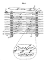
- FIG. 1 is a schematic end view showing one example of a 3D package for an electronic device made in accordance with the invention.
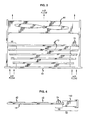
- FIG. 2 is a schematic top view of a circuit pack made in accordance with the invention, showing an alternate arrangement of cooling holes.
- FIG. 3 is a schematic end view showing an example of a 3D package having primary substrates of graduated size.
- FIG. 4 is a schematic end view of a circuit pack made in accordance with the invention, comprising an alternate cooling region in the form of a perforated or porous heat sink.
- As a pedagogical aid to a more complete understanding of the invention, a specific embodiment of the invention is described below.
- With reference to FIG. 1, circuit packs 10 are mounted on
bolts 20 and vertically interconnected to each other byconnective elements 30. Theconnective elements 30 are composed, for example, of material sold by AT&T under the tradename Conductive Polymer Interconnect (CPI). CPI is an elastic, compressible, sheet-like material that conducts electricity only in the vertical direction; i.e., in the direction perpendicular to the major surfaces of a sheet of the material. Thus, electrical connections between aligned contacts on facing surfaces of adjacent circuit packs are readily made by sandwiching a sheet of CPI between the circuit packs and slightly compressing the sheet between the circuit packs. Significantly, circuit packs that are interconnected in this manner are not separated by air gaps, because at least part of the space between them is filled by the CPI. As a result, it is impossible to air-cool such packages in the conventional way, by flowing air through air gaps between circuit packs in a direction substantially parallel to the major surfaces of the circuit packs. - Additional vertical spacing between successive circuit packs is readily achieved by sandwiching more than one sheet of CPI between the circuit packs.
Spacers 35 can be interposed between each pair of such CPI sheets. Suitable spacers comprise, for example, pieces of pc board containing vias, i.e., mutually electrically isolated, metal-lined holes capable of conducting electrical signals from one side of the pc board to the other. - Alternatively, the
connective elements 30 may be, for example, elements sold by AMP under the tradename Interposer, or button contacts sold under the tradename CIN-APSE by Cinch, a division of Labinal Components and Systems, Inc. - Each
circuit pack 10 comprises asubstrate 15, here called a primary substrate, having a pattern of electric conductors formed on it, and having one or moremultichip modules 40 mounted on it in electrical contact with the conductor pattern. The primary substrate is thermally conductive. Theprimary substrate 15 may be made, for example, from a thermally conductive ceramic material such as aluminum nitride or silicon carbide. Alternatively, the primary substrate may be a composite printed wiring board structure in which the conductor pattern is formed on one or both outer surfaces of a composite, multiple-layer laminated body. The outer, i.e., top and bottom, layers of the laminated body are relatively thin, e.g., about 20-mils-thick (0.51 mm thick), layers of conventional, polymeric material. The core layer, between the top and bottom layers, is a relatively thick, e.g., about 40-mils-thick (1.02 mm thick), layer of highly thermally conductive material. The total thickness of the primary substrate is desirably in the range 30-75 mils (0.76-1.91 mm). The thickness is preferably about 40 mils (1.02 mm) because although thermal resistance tends to fall off as the substrate is made thicker, such decrease is relatively shallow for substrate thicknesses greater than about 40 mils (1.02 mm). The separation between primary substrates is desirably in the range 75-200 mils (1.91-5.08 mm). For air cooling, the separation is preferably about 100 mils (2.54 mm) because empirical observations suggest that at such separation, the air-flow pattern provides particularly effective cooling. Advantageously, the core layer is not only thermally conductive, but also highly electrically conductive, so that it can also be used as an electrical ground plane. Thus a preferred material for the core layer is, for example, aluminum, or, alternatively, a copper-molybdenum composite having a thermal coefficient of expansion close to that of the silicon or ceramic substrates of the multichip modules. - The primary substrate has two major surfaces, i.e., a top surface and a bottom surface, on which a conductor pattern may be formed. In addition, if the primary substrate comprises a composite, multi-layer laminated body, additional electrically conductive layers, in addition to the core layer, are readily formed intermediate the top and bottom layers. Such intermediate conductive layers are separated and electrically insulated from one another by layers of, for example, polymeric or ceramic material. Electrical contact is readily made from multichip modules mounted on a primary substrate to intermediate conductive layers within the substrate via apertures extending through the overlying layers.
- The primary substrate represents the level of organization within the 3D package having a relatively large spatial scale. Thus, for example, the conductor pattern formed on the primary substrate typically has a line width of about 100-200 µm.
- Mounted on each
primary substrate 15 is at least onemultichip module 40. Each multichip module comprises a silicon orceramic substrate 45, here called a secondary substrate, having a pattern of electrical conductors formed on its top surface for electrically contactingintegrated circuits 50. Electrical conductors in the form, for example, of wirebonds are also provided, for electrically connecting the conductor pattern on the top surface of the secondary substrate to the conductor pattern on theprimary substrate 15 on which the multichip module is mounted. Mounted on the top surface of the secondary substrate, in electrical contact with the conductor pattern on that surface, is at least oneintegrated circuit 50. - The
secondary substrate 45 represents the level of organization within the 3D package having an intermediate spatial scale. Thus, for example, the conductor pattern formed on the secondary substrate typically has a line width of about 10-20 µm. ICs are mounted directly on the top surface of the secondary substrate. The ICs represent the level of organization having a relatively small spatial scale. Thus, for example, ICs typically have a linewidth of about 1 µm. - Each
primary substrate 15 has a pattern of electrical conductors formed on its top surface for electrically contacting themultichip modules 40 mounted on it, and may also have a similar pattern of electrical conductors on its bottom surface for mounting multichip modules on that surface as well. - Also formed on each primary substrate, in contact with the conductor patterns on that substrate, are contacts for electrically connecting the conductor patterns to the
connective elements 30. - Each
circuit pack 10 includes acooling region 55. For example, a cooling region is readily formed which comprises anouter portion 60 ofprimary substrate 15.Outer portion 60 is substantially free of multichip modules or attached electronic components. This outer portion is perforated, e.g., drilled, with a multiplicity ofholes 70.Outer portion 60 is intended to serve as a heat sink, and also as a heat exchanger, transferring heat from the primary substrate to air passing through the holes, as described below. Heat generated by the integrated circuits is conducted through thesecondary substrates 45, and from thesecondary substrates 45 to theprimary substrates 15. Within the primary substrates, heat is conducted from the regions adjacent the multichip modules, toward theouter portions 60. - Ambient air is drawn through the holes in
outer portions 60 by afan 80, mounted at one end, e.g., the top end, of the stack of circuit packs. The action of the fan is to vent air in the upward direction, as viewed in FIG. 1, so that air is drawn from, e.g., the bottom end of the stack upward, through the holes inouter portions 60, to the fan and from the fan out to the ambient atmosphere. An example of an appropriate fan for cooling, e.g., a 250-watt device, is the fan sold under the tradename Muffin-XL. - Heat conducted through
primary substrate 15 towardouter portion 60 is transferred at ornear holes 70 to air passing through the holes as a result of the action offan 80. Some heat is transferred through the walls of the holes to air (or other coolant fluid, e.g., coolant liquid impelled by a pump instead of a fan) passing through the holes. Significantly, it is believed that an even larger amount of heat is transferred to the cooling air (or other coolant fluid) from one or both major surfaces of the primary substrate. That is, the holes induce turbulence in the flow of coolant. It is believed that through mixing of warmer and cooler portions of the coolant fluid and/or regrowth of the boundary layer, this turbulence increases thermal contact between the coolant and those portions of the major surfaces that are adjacent to the holes. As a consequence, a substantial amount of heat is transferred from at least one major surface of each perforated base member to the coolant. - The sizes and distribution of cooling holes on a circuit pack are readily adjusted in accordance with local cooling requirements. For example, if a particular circuit pack has a substantially higher power dissipation level than neighboring circuit packs, the rate of heat transfer from that circuit pack to the cooling air can be enhanced by providing the outer portion of the corresponding primary substrate with smaller and more densely distributed holes.
- That is, the local rate of airflow may be greater in a smaller hole. Faster airflow can lead to greater turbulence, which can, in turn, increase the rate at which heat is transferred to the coolant fluid. Additionally, because the wall area of a hole is proportional to the square root of its facial area, smaller holes make more efficient use of substrate area in instances where substantial heat is transferred to coolant fluid through the walls of the holes.
- In addition, holes can be formed in portions of the circuit pack other than the outer portion, in order to enhance the rate of cooling near sources of high thermal power. For example, the hottest region of the circuit pack is often in the center. Thus, as depicted in FIG. 2, holes 70 can be readily formed in the central portion of a
circuit pack 10 in order to enhance the cooling of that portion. - In addition, as depicted, for example, in FIG. 3, the primary substrates are readily graduated in size in order to achieve a more uniform temperature distribution along the flow direction. That is, the cooling air tends to increase in temperature as it passes through successive circuit packs. As a result of the increase in temperature, the rate at which heat is transferred to the cooling air tends to decrease. This dropoff in cooling rate can be at least partially compensated by increasing the lateral extent of
outer portion 60 in order to increase its effectiveness as a heat sink, and by increasing the heat-exchange area. If theouter portion 60 is increased in lateral extent, the heat-exchange area is also readily increased by increasing the number ofholes 70. - Thus, even in a 3D package in which the power dissipation levels of the circuit packs vary by several hundred percent, the spatially averaged temperatures of all the circuit packs can be kept within a few Celsius degrees of each other by increasing the lateral extents of successive
outer portions 60, increasing the numbers of cooling holes accordingly, and using an appropriate airflow velocity. The growth direction is upward (see Fig. 1) or downstream; that is, outer portions that are nearer the fan are larger than outer portions that are farther from the fan. - A different example of cooling
region 55 comprises aheat distributing element 130, as depicted, for example, in FIG. 4.Element 130 comprises a highly thermally conductive, perforated or porous heat sink that is physically distinct fromprimary substrate 15.Element 130 is thermally conductively attached to an edge ofprimary substrate 15, for example, by engaging the substrate edge in a slot in the edge ofelement 130, and affixing the substrate with solder or thermally conductive epoxy adhesive. Cooling air passes through the holes or pores inelement 130 in a manner analogous to the passage of cooling air through the holes inouter portions 60.Elements 130 are readily used either in addition to, or instead of, perforatedouter portions 60. An example of aporous element 130 is an aluminum or copper sponge mounted in a metal frame. Cooling air, or other coolant fluid, passes readily through the pores or interstices in such a metallic sponge. - In addition, wherever cooling holes are used, whether in
outer portion 60 or inelement 130, the transfer of heat to the cooling air is readily further enhanced by placing porous, highly thermally conductive material within some or all of the holes, in thermal contact with the material defining the sides of the holes. An example of material suitable for that purpose is metal sponge, or, alternatively. folded wire similar to button contacts, but relatively loosely packed in order to offer relatively low flow resistance to the cooling air. - Referring back to FIG. 1, the signals entering and leaving the 3D package enter and leave by way of a
special circuit pack 90, here called the I/O circuit pack. The I/O circuit pack may occupy any circuit-pack position within the 3D package, and there may even be multiple I/O circuit packs. For ease of access, however, it is advantageous for the I/O circuit pack to be the bottom circuit pack (as viewed in FIG. 1); that is, the circuit pack occupying the end position farthest fromfan 80. Contacts are provided oncircuit pack 90 for electrically connecting electrical conductors bearing incoming or outgoing signals to the conductor pattern oncircuit pack 90. Optical signals may enter and leave the I/O circuit pack in addition to electrical signals, or alternatively to electrical signals. Optical connectors are readily provided oncircuit pack 90 for connecting incoming or outgoing lightwave channels, for example optical fibers, to optical or optoelectronic devices mounted oncircuit pack 90. - Like the other circuit packs, I/
O circuit pack 90 is readily provided with cooling holes in its outer portion. - In addition, I/
O circuit pack 90 is readily used as a mother board. That is, it is readily made substantially larger than the other circuit packs, and used for mounting of large electronic components, or, for example, power conditioning components. The interconnections between the components mounted oncircuit pack 90 may be, for example, by optical fibers, or by large-scale electrical means such as cables, or by small-scale means such as printed conductor patterns and wirebonds. Ifcircuit pack 90 belongs to an electronic device comprising more than one 3D package such as is described here,circuit pack 90 may be used as the I/O circuit pack for a multiplicity of 3D packages, each incorporating a portion ofcircuit pack 90 as a circuit pack occupying an end position. - Other embodiments of the invention are also useful. For example, the 3D package may be immersed in a liquid coolant, and an impeller, such as a pump, may be employed to force the liquid coolant to flow through the 3D package in a substantially vertical direction, through the holes in the circuit packs. In that case, heat is transferred from the circuit packs to the liquid coolant in a manner analogous to the air-cooling process described above. Heat is readily removed from the liquid coolant by contact with a heat exchanger.
- In a currently preferred embodiment, each primary substrate includes a copper core layer 12.7 cm square and 40 mils (1.02 mm) in thickness and has one major surface adapted for mounting four multichip modules. A peripheral area of the core layer about 1.5 cm wide, extending beyond the outer layers on all four sides, is perforated with cooling holes arranged in three staggered rows. The hole diameter is about 2.5 mm, and the separation between holes in the same row, and between the inner and outer rows, is about 0.8 cm. The vertical separation between primary substrates is about 2.5 mm. The hole patterns on alternate substrates are offset such that each hole falls on the median line between two holes of the preceding or following substrate.
- A stack of eight perforated heat sinks was cooled by an electric exhaust fan. The heat sinks were perforated aluminum plates 1.52 mm in thickness. The cooling region of each plate consisted of a peripheral region 25.4 mm wide. The holes in the plates were 3.18 mm in diameter, and arranged in staggered rows with a pitch of 8.89 mm. A cooling rate of 250 watts was measured, while temperatures near the centers of the plates were maintained at less than 85°C.
Claims (14)
a) at least two electronic subassemblies;
b) means for supporting the subassemblies in a stack such that the subassemblies overlap each other and are substantially perpendicular to a stacking axis;
c) cooling means comprising thermally conductive members having openings for the passage of coolant fluid through the members in a direction substantially parallel to the stacking axis; and
d) motivating means for causing a coolant fluid to pass through the openings;
CHARACTERIZED IN THAT
e) each electronic subassembly comprises: a base member having substantially planar first and second major surfaces that are substantially perpendicular to the stacking axis; a pattern of electric conductors formed on at least one of the major surfaces; and at least one integrated circuit mounted on a major surface in electrical contact with the conductor pattern;
f) the thermally conductive members are layers incorporated in the base members such that each base member incorporates at least one thermally conductive member; and
g) the openings are holes adapted to provide efficient mixing of the coolant fluid and enhanced thermal contact between the coolant fluid and at least one major surface of each of the base members.
a) at least two electronic subassemblies;
b) means for supporting the subassemblies in a stack such that the subassemblies overlap each other and are substantially perpendicular to a stacking axis;
c) cooling means comprising thermally conductive members having openings for the passage of coolant fluid through the members in a direction substantially parallel to the stacking axis; and
d) motivating means for causing a coolant fluid to pass through the openings;
CHARACTERIZED IN THAT
e) each electronic subassembly comprises: a base member having essentially planar first and second major surfaces that are substantially perpendicular to the stacking axis; a pattern of electric conductors formed on at least one of the major surfaces; and at least one multichip module mounted on a major surface in electrical contact with the conductor pattern;
f) the thermally conductive members are copper core layers, about 40 mils (1.02 mm) in thickness, one such core layer being incorporated in each base member, each core layer having four sides and a peripheral region extending around all four sides;
g) the openings are holes passing through the peripheral regions, the holes being adapted to provide efficient thermal contact between the coolant fluid and at least one major surface of each of the base members; and
h) the vertical separation between subassemblies is at least about 75 mils (1.91 mm) but not more than about 200 mils (5.08 mm).
Applications Claiming Priority (4)
| Application Number | Priority Date | Filing Date | Title |
|---|---|---|---|
| US38748089A | 1989-07-28 | 1989-07-28 | |
| US387480 | 1989-07-28 | ||
| US519728 | 1990-05-10 | ||
| US07/519,728 US5049982A (en) | 1989-07-28 | 1990-05-10 | Article comprising a stacked array of electronic subassemblies |
Publications (3)
| Publication Number | Publication Date |
|---|---|
| EP0410631A2 true EP0410631A2 (en) | 1991-01-30 |
| EP0410631A3 EP0410631A3 (en) | 1992-03-18 |
| EP0410631B1 EP0410631B1 (en) | 1997-03-26 |
Family
ID=27011889
Family Applications (1)
| Application Number | Title | Priority Date | Filing Date |
|---|---|---|---|
| EP90307844A Expired - Lifetime EP0410631B1 (en) | 1989-07-28 | 1990-07-18 | Article comprising a stacked array of electronic subassemblies |
Country Status (4)
| Country | Link |
|---|---|
| US (1) | US5049982A (en) |
| EP (1) | EP0410631B1 (en) |
| JP (1) | JPH0671057B2 (en) |
| DE (1) | DE69030288T2 (en) |
Cited By (4)
| Publication number | Priority date | Publication date | Assignee | Title |
|---|---|---|---|---|
| EP0465196A2 (en) * | 1990-07-02 | 1992-01-08 | General Electric Company | Compact high density interconnect structure |
| EP0555659A2 (en) * | 1992-02-14 | 1993-08-18 | International Business Machines Corporation | Multi-chip Module |
| WO1993024955A1 (en) * | 1992-05-25 | 1993-12-09 | Mannesmann Ag | Fluid-cooled power transistor arrangement |
| FR2760593A1 (en) * | 1997-01-27 | 1998-09-11 | Hughes Aircraft Co | Electronic assembly with high heat dissipation |
Families Citing this family (42)
| Publication number | Priority date | Publication date | Assignee | Title |
|---|---|---|---|---|
| US5343447A (en) * | 1990-05-23 | 1994-08-30 | Olympus Optical Co., Ltd. | Self-cooling optomagnetic disk device with locking internal mechanism |
| US5590345A (en) * | 1990-11-13 | 1996-12-31 | International Business Machines Corporation | Advanced parallel array processor(APAP) |
| US5588152A (en) * | 1990-11-13 | 1996-12-24 | International Business Machines Corporation | Advanced parallel processor including advanced support hardware |
| US5630162A (en) * | 1990-11-13 | 1997-05-13 | International Business Machines Corporation | Array processor dotted communication network based on H-DOTs |
| US5734921A (en) * | 1990-11-13 | 1998-03-31 | International Business Machines Corporation | Advanced parallel array processor computer package |
| US5963746A (en) * | 1990-11-13 | 1999-10-05 | International Business Machines Corporation | Fully distributed processing memory element |
| US5966528A (en) * | 1990-11-13 | 1999-10-12 | International Business Machines Corporation | SIMD/MIMD array processor with vector processing |
| US5625836A (en) * | 1990-11-13 | 1997-04-29 | International Business Machines Corporation | SIMD/MIMD processing memory element (PME) |
| US5765012A (en) * | 1990-11-13 | 1998-06-09 | International Business Machines Corporation | Controller for a SIMD/MIMD array having an instruction sequencer utilizing a canned routine library |
| US5815723A (en) * | 1990-11-13 | 1998-09-29 | International Business Machines Corporation | Picket autonomy on a SIMD machine |
| US5752067A (en) * | 1990-11-13 | 1998-05-12 | International Business Machines Corporation | Fully scalable parallel processing system having asynchronous SIMD processing |
| US5809292A (en) * | 1990-11-13 | 1998-09-15 | International Business Machines Corporation | Floating point for simid array machine |
| US5963745A (en) * | 1990-11-13 | 1999-10-05 | International Business Machines Corporation | APAP I/O programmable router |
| US5794059A (en) * | 1990-11-13 | 1998-08-11 | International Business Machines Corporation | N-dimensional modified hypercube |
| ATE180586T1 (en) * | 1990-11-13 | 1999-06-15 | Ibm | PARALLEL ASSOCIATIVE PROCESSOR SYSTEM |
| US5828894A (en) * | 1990-11-13 | 1998-10-27 | International Business Machines Corporation | Array processor having grouping of SIMD pickets |
| US5765011A (en) * | 1990-11-13 | 1998-06-09 | International Business Machines Corporation | Parallel processing system having a synchronous SIMD processing with processing elements emulating SIMD operation using individual instruction streams |
| US5765015A (en) * | 1990-11-13 | 1998-06-09 | International Business Machines Corporation | Slide network for an array processor |
| US5617577A (en) * | 1990-11-13 | 1997-04-01 | International Business Machines Corporation | Advanced parallel array processor I/O connection |
| US5304845A (en) * | 1991-04-09 | 1994-04-19 | Digital Equipment Corporation | Apparatus for an air impingement heat sink using secondary flow generators |
| US5594918A (en) * | 1991-05-13 | 1997-01-14 | International Business Machines Corporation | Parallel computer system providing multi-ported intelligent memory |
| US5168348A (en) * | 1991-07-15 | 1992-12-01 | International Business Machines Corporation | Impingment cooled compliant heat sink |
| US5200631A (en) * | 1991-08-06 | 1993-04-06 | International Business Machines Corporation | High speed optical interconnect |
| DE69218913T2 (en) * | 1992-01-31 | 1997-07-17 | Cit Alcatel | Method for determining the transit time between a remote end station and a central end station, in a bidirectional point-to-multipoint transmission system |
| JP2642039B2 (en) * | 1992-05-22 | 1997-08-20 | インターナショナル・ビジネス・マシーンズ・コーポレイション | Array processor |
| DE69330450T2 (en) * | 1992-08-05 | 2001-11-08 | Fujitsu Ltd | Three-dimensional multichip module |
| US5854534A (en) * | 1992-08-05 | 1998-12-29 | Fujitsu Limited | Controlled impedence interposer substrate |
| US5334029A (en) * | 1993-05-11 | 1994-08-02 | At&T Bell Laboratories | High density connector for stacked circuit boards |
| US6110306A (en) * | 1999-11-18 | 2000-08-29 | The United States Of America As Represented By The Secretary Of The Navy | Complexed liquid fuel compositions |
| WO2001080561A1 (en) * | 2000-04-18 | 2001-10-25 | Rtimage Inc. | System and method for the lossless progressive streaming of images over a communication network |
| US6977346B2 (en) * | 2002-06-10 | 2005-12-20 | Visteon Global Technologies, Inc. | Vented circuit board for cooling power components |
| DE10243026B3 (en) * | 2002-09-13 | 2004-06-03 | Oliver Laing | Device for local cooling or heating of an object |
| US20040115995A1 (en) * | 2002-11-25 | 2004-06-17 | Sanders Samuel Sidney | Circuit array module |
| US20040160742A1 (en) * | 2003-02-14 | 2004-08-19 | Weiss Roger E. | Three-dimensional electrical device packaging employing low profile elastomeric interconnection |
| US20070089902A1 (en) * | 2005-10-25 | 2007-04-26 | Tourne Joseph A | Circuit board having a multi-signal via |
| JP4885529B2 (en) * | 2005-12-08 | 2012-02-29 | 住友重機械工業株式会社 | Radiation detection unit and radiation inspection apparatus |
| US7432702B2 (en) * | 2005-12-22 | 2008-10-07 | Honeywell International Inc. | Circuit board damping assembly |
| US20090226696A1 (en) * | 2008-02-06 | 2009-09-10 | World Properties, Inc. | Conductive Polymer Foams, Method of Manufacture, And Uses Thereof |
| US8623265B2 (en) * | 2007-02-06 | 2014-01-07 | World Properties, Inc. | Conductive polymer foams, method of manufacture, and articles thereof |
| WO2008097571A1 (en) * | 2007-02-06 | 2008-08-14 | World Properties, Inc. | Conductive polymer foams, method of manufacture, and uses thereof |
| JP2013515840A (en) * | 2009-12-29 | 2013-05-09 | ロジャース コーポレーション | Conductive polymer foam, its production method and use |
| JP5758584B2 (en) * | 2010-03-18 | 2015-08-05 | 本田技研工業株式会社 | Junction box |
Citations (3)
| Publication number | Priority date | Publication date | Assignee | Title |
|---|---|---|---|---|
| US4536824A (en) * | 1983-03-28 | 1985-08-20 | Goodyear Aerospace Corporation | Indirect cooling of electronic circuits |
| US4839774A (en) * | 1988-01-25 | 1989-06-13 | Digital Equipment Corporation | Apparatus and method for cooling electronic component packages using an array of directed nozzles fabricated in the circuit board |
| US4841355A (en) * | 1988-02-10 | 1989-06-20 | Amdahl Corporation | Three-dimensional microelectronic package for semiconductor chips |
Family Cites Families (2)
| Publication number | Priority date | Publication date | Assignee | Title |
|---|---|---|---|---|
| US3727114A (en) * | 1971-08-03 | 1973-04-10 | Mitsubishi Electric Corp | Air cooled semiconductor stack |
| JPS60234762A (en) * | 1984-05-03 | 1985-11-21 | Toyoda Autom Loom Works Ltd | Method and device for producing fiber reinforced molding |
-
1990
- 1990-05-10 US US07/519,728 patent/US5049982A/en not_active Expired - Lifetime
- 1990-07-18 DE DE69030288T patent/DE69030288T2/en not_active Expired - Fee Related
- 1990-07-18 EP EP90307844A patent/EP0410631B1/en not_active Expired - Lifetime
- 1990-07-26 JP JP2196409A patent/JPH0671057B2/en not_active Expired - Lifetime
Patent Citations (3)
| Publication number | Priority date | Publication date | Assignee | Title |
|---|---|---|---|---|
| US4536824A (en) * | 1983-03-28 | 1985-08-20 | Goodyear Aerospace Corporation | Indirect cooling of electronic circuits |
| US4839774A (en) * | 1988-01-25 | 1989-06-13 | Digital Equipment Corporation | Apparatus and method for cooling electronic component packages using an array of directed nozzles fabricated in the circuit board |
| US4841355A (en) * | 1988-02-10 | 1989-06-20 | Amdahl Corporation | Three-dimensional microelectronic package for semiconductor chips |
Cited By (6)
| Publication number | Priority date | Publication date | Assignee | Title |
|---|---|---|---|---|
| EP0465196A2 (en) * | 1990-07-02 | 1992-01-08 | General Electric Company | Compact high density interconnect structure |
| EP0465196A3 (en) * | 1990-07-02 | 1992-03-11 | General Electric Company | Compact high density interconnect structure |
| EP0555659A2 (en) * | 1992-02-14 | 1993-08-18 | International Business Machines Corporation | Multi-chip Module |
| EP0555659A3 (en) * | 1992-02-14 | 1993-12-22 | Ibm | Multi-chip module |
| WO1993024955A1 (en) * | 1992-05-25 | 1993-12-09 | Mannesmann Ag | Fluid-cooled power transistor arrangement |
| FR2760593A1 (en) * | 1997-01-27 | 1998-09-11 | Hughes Aircraft Co | Electronic assembly with high heat dissipation |
Also Published As
| Publication number | Publication date |
|---|---|
| EP0410631B1 (en) | 1997-03-26 |
| DE69030288D1 (en) | 1997-04-30 |
| US5049982A (en) | 1991-09-17 |
| JPH03124053A (en) | 1991-05-27 |
| DE69030288T2 (en) | 1997-09-25 |
| EP0410631A3 (en) | 1992-03-18 |
| JPH0671057B2 (en) | 1994-09-07 |
Similar Documents
| Publication | Publication Date | Title |
|---|---|---|
| US5049982A (en) | Article comprising a stacked array of electronic subassemblies | |
| US4884168A (en) | Cooling plate with interboard connector apertures for circuit board assemblies | |
| US7233501B1 (en) | Interleaved memory heat sink | |
| US7400505B2 (en) | Hybrid cooling system and method for a multi-component electronics system | |
| US5826643A (en) | Method of cooling electronic devices using a tube in plate heat sink | |
| US9456527B2 (en) | Fabricating separable and integrated heat sinks facilitating cooling multi-component electronic assembly | |
| US5304846A (en) | Narrow channel finned heat sinking for cooling high power electronic components | |
| US6496367B2 (en) | Apparatus for liquid cooling of specific computer components | |
| US6055157A (en) | Large area, multi-device heat pipe for stacked MCM-based systems | |
| US5986882A (en) | Electronic apparatus having removable processor/heat pipe cooling device modules therein | |
| US6466441B1 (en) | Cooling device of electronic part having high and low heat generating elements | |
| US5088005A (en) | Cold plate for cooling electronics | |
| US5036384A (en) | Cooling system for IC package | |
| US6496375B2 (en) | Cooling arrangement for high density packaging of electronic components | |
| US4283754A (en) | Cooling system for multiwafer high density circuit | |
| US5294831A (en) | Circuit pack layout with improved dissipation of heat produced by high power electronic components | |
| US20050018406A1 (en) | Stack up assembly | |
| JPH0563119B2 (en) | ||
| US7145775B2 (en) | Chassis conducted cooling thermal dissipation apparatus for servers | |
| US20080192428A1 (en) | Thermal management system for computers | |
| JP2901835B2 (en) | Semiconductor device | |
| EP0630521A1 (en) | Three dimensional, multi-chip module | |
| US5812372A (en) | Tube in plate heat sink | |
| US10721838B1 (en) | Stacked base heat sink with heat pipes in-line with airflow | |
| US5343359A (en) | Apparatus for cooling daughter boards |
Legal Events
| Date | Code | Title | Description |
|---|---|---|---|
| PUAI | Public reference made under article 153(3) epc to a published international application that has entered the european phase |
Free format text: ORIGINAL CODE: 0009012 |
|
| AK | Designated contracting states |
Kind code of ref document: A2 Designated state(s): DE FR GB |
|
| PUAL | Search report despatched |
Free format text: ORIGINAL CODE: 0009013 |
|
| AK | Designated contracting states |
Kind code of ref document: A3 Designated state(s): DE FR GB |
|
| 17P | Request for examination filed |
Effective date: 19920904 |
|
| RAP3 | Party data changed (applicant data changed or rights of an application transferred) |
Owner name: AT&T CORP. |
|
| 17Q | First examination report despatched |
Effective date: 19940907 |
|
| GRAG | Despatch of communication of intention to grant |
Free format text: ORIGINAL CODE: EPIDOS AGRA |
|
| GRAH | Despatch of communication of intention to grant a patent |
Free format text: ORIGINAL CODE: EPIDOS IGRA |
|
| GRAH | Despatch of communication of intention to grant a patent |
Free format text: ORIGINAL CODE: EPIDOS IGRA |
|
| GRAA | (expected) grant |
Free format text: ORIGINAL CODE: 0009210 |
|
| AK | Designated contracting states |
Kind code of ref document: B1 Designated state(s): DE FR GB |
|
| REF | Corresponds to: |
Ref document number: 69030288 Country of ref document: DE Date of ref document: 19970430 |
|
| ET | Fr: translation filed | ||
| PLBE | No opposition filed within time limit |
Free format text: ORIGINAL CODE: 0009261 |
|
| STAA | Information on the status of an ep patent application or granted ep patent |
Free format text: STATUS: NO OPPOSITION FILED WITHIN TIME LIMIT |
|
| 26N | No opposition filed | ||
| PGFP | Annual fee paid to national office [announced via postgrant information from national office to epo] |
Ref country code: FR Payment date: 20010625 Year of fee payment: 12 |
|
| PGFP | Annual fee paid to national office [announced via postgrant information from national office to epo] |
Ref country code: GB Payment date: 20010628 Year of fee payment: 12 |
|
| PGFP | Annual fee paid to national office [announced via postgrant information from national office to epo] |
Ref country code: DE Payment date: 20010928 Year of fee payment: 12 |
|
| REG | Reference to a national code |
Ref country code: GB Ref legal event code: IF02 |
|
| PG25 | Lapsed in a contracting state [announced via postgrant information from national office to epo] |
Ref country code: GB Free format text: LAPSE BECAUSE OF NON-PAYMENT OF DUE FEES Effective date: 20020718 |
|
| PG25 | Lapsed in a contracting state [announced via postgrant information from national office to epo] |
Ref country code: DE Free format text: LAPSE BECAUSE OF NON-PAYMENT OF DUE FEES Effective date: 20030201 |
|
| GBPC | Gb: european patent ceased through non-payment of renewal fee |
Effective date: 20020718 |
|
| PG25 | Lapsed in a contracting state [announced via postgrant information from national office to epo] |
Ref country code: FR Free format text: LAPSE BECAUSE OF NON-PAYMENT OF DUE FEES Effective date: 20030331 |
|
| REG | Reference to a national code |
Ref country code: FR Ref legal event code: ST |