EP0424191A2 - Device and method for defect handling in semi-conductor memory - Google Patents
Device and method for defect handling in semi-conductor memory Download PDFInfo
- Publication number
- EP0424191A2 EP0424191A2 EP19900402578 EP90402578A EP0424191A2 EP 0424191 A2 EP0424191 A2 EP 0424191A2 EP 19900402578 EP19900402578 EP 19900402578 EP 90402578 A EP90402578 A EP 90402578A EP 0424191 A2 EP0424191 A2 EP 0424191A2
- Authority
- EP
- European Patent Office
- Prior art keywords
- defects
- data
- list
- information list
- memory
- Prior art date
- Legal status (The legal status is an assumption and is not a legal conclusion. Google has not performed a legal analysis and makes no representation as to the accuracy of the status listed.)
- Granted
Links
Images


Classifications
-
- G—PHYSICS
- G11—INFORMATION STORAGE
- G11C—STATIC STORES
- G11C29/00—Checking stores for correct operation ; Subsequent repair; Testing stores during standby or offline operation
- G11C29/70—Masking faults in memories by using spares or by reconfiguring
- G11C29/76—Masking faults in memories by using spares or by reconfiguring using address translation or modifications
- G11C29/765—Masking faults in memories by using spares or by reconfiguring using address translation or modifications in solid state disks
Definitions
- This invention relates generally to semi-conductor memory, and more specifically to a simplified scheme for accessing sequential data in a non-volatile memory such as an EEprom or Flash EEprom memory and handling the defects therein.
- Semi-conductor memory is formed as an integrated circuit (IC) device with a two-dimensional array of memory cells arrayed in rows and columns. Each cell contains a transistor which can be put into one of its conduction states designating one of the memory states.
- IC integrated circuit
- disk drives are disadvantageous in that they are bulky and in their requirement for high precision moving mechanical parts. Consequently, they are not rugged, and are complicated and prone to reliability problems, as well as consuming significant amounts of power.
- RAM Random Access Memory
- ROM Read only Memory
- PROM Programmable read-only memory
- UVEPROM UV Erasable PROM
- EEprom Electrically Erasable programmable read-only memory
- Flash EEprom Flash EEprom
- ROM, EEprom and Flash EEprom are all non-volatile solid state memories. They retain their memory even after power is shut down. However, ROM and PROM cannot be reprogrammed. UVPROM cannot be erased electrically. On the other hand, EEprom and Flash EEprom have the further advantage of being electrically writable (or programmable) and erasable. Nevertheless, conventional EEprom and Flash EEprom have a limited lifetime due to the endurance-related stress the device suffers each time it goes through an erase/program cycle. The endurance of a Flash EEprom device is its ability to withstand a given number of program/erase cycles.
- the physical phenomenon limiting the endurance of conventional EEprom and Flash EEprom devices is trapping of electrons in the active dielectric films of the device.
- electrons are injected from the substrate to the floating gate through a dielectric interface.
- electrons are extracted from the floating gate to the erase gate through a dielectric interface.
- some of the electrons are trapped by the dielectric interface.
- the trapped electrons oppose the applied electric field in subsequent program/erase cycles thereby causing the programmed threshold voltage to shift to a lower value and the erased threshold voltage to shift to a higher value. This can be seen in a gradual closure in the threshold voltage "window" between the "0" and "1" states. Beyond approximately l x 10.
- the window closure can become sufficiently severe to cause the reading circuitry to malfunction. If cycling is continued, the device eventually experiences catastrophic failure due to a ruptured dielectric. This typically occurs at between 1 x 10⁶ and 1 x 10⁷ cycles, and is known as the intrinsic breakdown of the device. Thus, with use, defects tend to build up in the memory array and typically the devices are rendered unreliable after 103 to 104 write/erase cycles.
- EEprom and Flash EEprom are used in applications where semi-permanent storage of data or program is required but with a limited need for reprogramming.
- ECC Error Correction Code
- Another way of treating defects in EEprom and Flash EEprom is to use schemes similar to defect remapping in disks.
- the medium In the normal disk system the medium is divided into cylinders and sectors, the sector being the basic unit in which data is stored.
- a controller is used to manage the operations of the disk and handle defect remapping. Before use, the medium must be initialized (or "formatted") to remap the defects. The system is partitioned into the various sectors. The sectors containing the defects are identified and are marked as bad and not to be used by the system. This is done in several ways.
- a defect map table is stored on a particular portion of the disk to be used by the interfacing controller. Normally, it is located both in the drive directory and in the header field of a data sector.
- the bad sectors are marked as bad by special I.D. and flag markers.
- the defect is at an address, the data that would normally be stored there is placed in an alternative location.
- the requirement for alternative sectors makes the system assigns spare sectors at some specific interval or location. This reduces the amount of memory capacity and is a performance issue in how the alternative sectors are located.
- the alternative sector remapping is not necessarily sequential with the rest of the data. Generally a sophisticated and expensive controller with microprocessor intelligence is required to handle this type of defect management.
- An example of defect mapping in EEprom system is disclosed in copending U.S. Patent application, Serial No. 337,566, filed April 13, 1989, entitled "Flash EEprom System.” The copending application is assigned to the same assignee of the present application and the disclosure of which is hereby incorporated by reference.
- One application of the present invention is in the storage of sequential data in a portable and detachable EEprom or Flash EEprom device. Examples would be in data logging, audio or image data applications.
- the device is in a detachable format functionally similar to magnetic tape cassettes or floppy disks.
- the invention takes advantage of the sequential nature of the data and the limited operations required by a field recording device. Because each data file is written in integral of a whole file by a long series of sequential write and not in a random access fashion, and new files are appended after the last written one, the controller needs only support simple append operations. In another implementation it may also support sequential read operations. Other functionalities such as erase and initialization may be furnished, when required, by attaching the memory medium to other systems having controllers with such capabilities. Thus by distributing the functionalities into several specialized controllers, each controller may be simplified.
- the sequential writing and reading of the data in the memory also allows a defect list of the memory device to be ordered sequentially with the data.
- the defect list is scanned along with data access of memory locations, so that the locations, integrity can be checked simply by sequentially inspecting the current entry in the defect list.
- a solid-state memory such as an EEprom or Flash EEprom memory array is partitioned into a user data portion and a first information list portion.
- the user data portion or user memory is used for storing user data.
- the first information list includes a directory of previously detected defects. The defects are ordered sequentially in the same way as data is stored in the data portion.
- a controller references the defects listed in the first information list while accessing the user data portion. Any locations containing a defect are skipped over.
- addressing and referencing by the controller is simplified to stepping sequentially to the next location in the user memory and after a defect is processed to the next defect on the list and comparing the next location address with the next defect address from the list.
- the first information list includes an ordered list of column defects and an ordered list of other defects previously detected. Both defect lists are referenced when writing to and reading from the user memory.
- the memory is further partitioned into a second information list.
- This list is maintained by the controller and provides an ordered directory of files written in the user data portion and any defects detected in the user data portion during writing.
- the second information list is referenced sequentially together with the first list by the controller in a read operation such that any locations containing a listed defect are skipped over.
- a method of handling defects in solid-state memory includes assigning an ordered addressing system to the memory, detecting defects in the memory prior to commencing writing a file to the memory, storing in the memory a first list of the defects, addresses and types, and referencing the first list for skipping over the defects while accessing the memory.
- the method of the present invention also includes writing data files to the memory, storing in a second ordered list in the memory file-markers of data files, verifying each write operation, skipping over defects detected in failures in write verifications, and storing the addresses and the type of the defects detected in the second ordered list.
- the method of the present invention also includes reading data files from the memory, and skipping over the defects by referencing the first and second ordered lists.
- the restricted functionality and the data structure allow a simple and low cost controller without the need for microprocessor intelligence, and yet be able to handle defects endemic to EEprom or Flash EEprom and other solid-state memory devices.
- Figure 1 illustrates a system of semiconductor memory.
- it comprises one or more non-volatile, EEprom or Flash EEprom memory devices 10, 12 managed by a controller 20 via an address/data bus 30 and a control bus 40.
- the control bus 40 carries various control, clock and miscellaneous handshake signals, if any. In other embodiments, some of the above buses can be combined into multiplexed buses or separated into single purpose buses.
- the controller 20 itself is connected to a larger system (not shown) via system address/data bus 50 and system control bus 60.
- the larger system may be a microprocessor based system or other digital system such as a data collecting system.
- the system is typically used for logging sequential data, and therefore the controller 20 is only required to perform simple write operations and/or read operations on the memory devices 10, 12.
- the EEprom or Flash EEprom memory devices 10 or 12 may be detached from the system and be re-connected to another, full-feature system for other operations such as initialization and erase.
- Copending U.S. Patent application, Serial No. 337,579, filed April 13, 1989, entitled “Multi-state EEprom Read and Write circuits and techniques,” discloses an EEprom system capable of various operations, the disclosure of which is hereby incorporated by reference.
- Figure 2 shows a two dimensional array of memory cells 100 arranged in rows and columns.
- the memory array 100 is the storage part of the memory device such as 10, 12. Before the memory array is used for the first time, any existing defects are treated by an initialization process, much like that of formatting in magnetic disks.
- a bit defect occurs when a single cell such as 102 is defective.
- a column defect such as 104, 106 can occur when a whole column of cells is shorted.
- a row defect 108 occurs when a whole row of cells are rendered inoperative.
- Flash EEprom device Even after the initially detected defects are handled, the nature of the Flash EEprom device tends to have more and more cell failures with increasing write/erase cycling. ECC is used to correct a limited number of random errors that may arise in between write and read operations. However, the errors from the defective cells that accumulate with use will eventually overwhelm the ECC and render the device unusable.
- One important feature of the present invention is the ability of the system also to detect and handle these defects on-the-fly. Defective cells are detected by their failure to write correctly. As soon as a defective cell is identified, the controller skips over the defect location while accessing the memory and adds the new defect to the defect list. This dynamic handling of defects, in addition to conventional error correction schemes, significantly increases the reliability and prolongs the life of the device.
- the present invention is concerned with the storage of data which are sequential or quasi-sequential in their use of the storage in the memory.
- Managing defects in the memory array requires listing the defects found and referencing the listed defects while accessing the memory, thereby being able to avoid using locations occupied by these defects in the array.
- the memory space is partitioned into three portions as illustrated in Figure 3A.
- User data portion or user memory 110 fills up from one end (e.g. bottom) of the memory array 10.
- the other two portions are located at the other end (top) of the memory array 100.
- the first portion is where the static information list 120 resides. It has a size which is fixed at initialization of the memory device.
- the second portion preferably begins where the first portion ends and is where the dynamic information list 130 resides.
- the user data portion 110 is for a user to store data files.
- the static information list 120 contains the starting address of the dynamic information list as well as information about defects known at initialization of the memory array 100. It is written there at initialization and remains unchanged until the next initialization at which time any additional defects which have been detected are incorporated into the new list.
- the dynamic information list 130 essentially logs the write history of the user data portion 110 since the last initialization. It is maintained by the controller 20 and is a directory (file markers) of data files which have been written in the user data portion 110 as well as any defects found during write verification.
- the user data portion 110 and the dynamic information list may be regarded as sharing the same memory space.
- the dynamic information list 130 fills from the other end (e.g. top down), with free memory space in between. In this way, allowance is made to accommodate the variable size of the user data portion and the dynamic information list portion. In the event when the two portions meet, the memory capacity is completely filled and no further data may be written.
- Figure 3B shows an alternative arrangement in which the static information list 120 is written at one end (e.g. bottom) of the memory array 100 at initialization.
- the user data portion 110 extends upwards from where the static information list 120 ends.
- the dynamic information list 130 begins from the top end of the memory array 100 and extends downwards.
- One important feature of the present invention is the requirement that the data being written to the memory array is sequential. This allows simplification in addressing by restricting the write operation to be an append operation. Thus new files must always be appended at the end of the last written file.
- This architecture allows ordered lists to be built for both the static information list 120 and the dynamic information list 130. As a result, addressing and defect tracking are greatly simplified.
- the memory array 100 shown in Figures 3A and 3B is a two dimensional array of memory cells arranged in rows and columns.
- the memory array 100 is filled in a definite sequence from one end to another end.
- the memory space is filled row by row.
- data will fill across the bottom row starting from the cell in the first column.
- the data will move up to the next row starting from the cell in the first column again.
- the contents of the static information list 120 and the dynamic information list 130 fill the memory space in similar manner except they start from the top of the memory space and fill row by row downwards.
- the memory array 100 is two-dimensional, it will be understood that discussion of rows and columns are interchangeable. Thus it is equally applicable to fill the memory column by column. Indeed, since the two-dimensional array may be randomly accessed, it could be filled in any prescribed order. All these cases are within the scope of the present protected invention.
- Figure 4A illustrates schematically the contents of the user data portion 110, the static information list 120 and the dynamic information list 130.
- the three portions of the memory array 100 are illustrated schematically as three linear memory arrays each with a starting location at the bottom and an ending location at the top.
- the current access positions on the user data portion 110, the static information list 120 and the dynamic information list 130 are respectively denoted by arrows 101, 103, 105.
- the memory array Before the memory array is used for the first time after it is manufactured, it is tested for defects. Defects detected are treated by an initialization process, much like that of formatting in magnetic disks. The initialization may be done at the factory. Essentially, a memory tester is used to locate the various defects and their types. Any defects detected in the user data portion 110 at this stage will be recorded in the static information list 120 in the order they occur in the user data portion.
- the static column defects are treated at the same level as the other static defects.
- the addresses of all static defects are placed on the static information list 120 as one list and in the order they appear in the user data portion 110. They static column defects will therefore appear in the list 120 periodically.
- the static information list 120 will be referenced by the controller 20 in order to skip over the defects listed in the list.
- the column defects are preferably isolated from the rest of the defects in the static information list 120 and placed in a separate static column defect list 150 (see Figure 4B.) This is done at initialization.
- the list 150 is an ordered subdirectory of column defects and may be regarded as part of the static information list 120 which resides in the memory array 100.
- column defects 104, 106 cut across the rows in the user data portion 110. If the memory is filled row by row, these column defects will be encountered at every row at the same column locations. Since these defects come up frequently and regularly, they are preferably collected in a separate static column defect list 150 instead of manifesting in multiples and periodically in the list 120.
- both the static column defect list 150 and the other defects listed in the static information list 120 will be referenced by the controller 20 in order to skip over all the defects listed.
- the static column defect list 150 Since the static column defect list 150 is referenced during accessing of every row, it may be partially or preferably fully buffered into the controller and placed in a storage 140 for easy access prior to a write or read operation. In this way, the column defect list can be accessed quickly and efficiently in the controller 20 without having to fetch them every time from the static information list located in the memory device 10.
- the current position in the static column defect list 150 which also resides in the storage 140 is denoted by an arrow 141.
- the static information list 120 As the static information list 120 is being compiled and written to the memory array 100, care must be taken not to lay it on any possible defective locations therein.
- One way of handling defects in the portion where the static information list 120 resides is to use a highly redundant code for coding the information list as well as marking the defective locations of the information list. In this way when a code designating the present location in the information list as defective is written to that defective location, it is still recognizable as such, even though it may have been somewhat corrupted.
- the controller avoids laying the static information list in locations where defects are detected in the portion for the list 120 and also marks those locations as defective with a code.
- the controller will then be able to detect the bad locations and skip over them.
- Other ways of handling defects in the information lists include the use of redundant lists and discarding any highly defective device which could not be handled by the schemes described.
- the controller puts the starting address of file1 in the dynamic information list 130 and begins to write the content of filel sequentially into user memory 110.
- defects are handled in two ways depending on whether the defects are found at initialization or are found during a write-verify failure.
- the static information list 120 is examined to see if that new location coincides with a defect. If a defect such as DC1 or D1 exists, the defective location will be skipped and data is written to the next good location.
- Each write can be followed by a verification step. (An improved EEprom or Flash EEprom device with write-verification is also disclosed in co-pending U.S. Patent application, Serial No. 337,579, and pertinent portions of which are hereby incorporated by reference.) If a write fails to be verified correctly at a location, that location is declared defective and data is written onto the next good location.
- the write-verify-failure defect address is stored in the dynamic information list 130 for future reference.
- the dynamic information list 130 must not be laid on any possible defective locations in the memory array 100.
- the technique for avoiding possible defect locations are similar to that of the static information list 120 described earlier.
- the dynamic information list 130 effectively logs the write history of the user memory 110. It contains an ordered list of file markers (addresses and/or file-identifers) and addresses of embedded defects that were discovered during the course of writing the files. Since the write operation is sequential, both the file markers designating the addresses and/or file-identifers of the written files and the defect addresses will automatically be put in the order they occurred in the user data portion 110.
- a tag 152 associated with each address listed in the dynamic information list identifies whether the address refers to a file nmarker or a defect of a certain type.
- file markers include Start-Of-List, End-Of-List, Start-Of-File and End-Of-File and File-Identifier.
- the information in the dynamic information list is
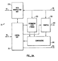
- Figure 5A is a schematic circuit block diagram illustrating the functional blocks within the controller for implementing write and read operations incorporating defect handling.
- the controller 20 is comprised of a control unit 210, information lists storage 220, pointers 230, comparators 240 and a data manipulation unit 250. As in Figure 1, the controller 20 is in communication with a larger system via a system address/data bus 50 and a system control bus 60. The controller is also detachably connected with memory devices 10, 12 via an output data bus 251, and output address bus 253 and an output control bus 255.
- Figure 5B illustrates the components included in the information lists storage block 220 of the controller.
- One component is a static information list storage 222 which is used for storing items retrieved from the static information list 120. In particular, during defect processing, the storage 222 is used for storing the address and type of the current static defect.
- a second component is the static column defect list storage 140 mentioned before. It is used to store a partial, or preferably complete, list of column defects 150 which is buffered into the controller prior to the first write or read operation.
- a third component is a dynamic information list storage 224 which is used for storing items retrieved from the dynamic information list 130.
- Figure 5C illustrates the components included in the pointers block 230 of the controller. It includes a data pointer 232, a static information list pointer 234, a static column defect list pointer 236 and a dynamic information list pointer 238.
- the pointers 232, 234, 236, 238 respectively hold the addresses for accessing the user data portion 110, the static information list 120, the static column defect list 140 and the dynamic information list 130.
- Figure 5D illustrates the components included in the data manipulation unit block 250 of the controller.
- the data manipulation unit 250 is under the control of the control unit 210 (see Figure 5A.) It comprises a system I/O buffer 262, a staging buffer 264 and a write/read block buffer 266.
- data from the system address/data bus 50 is buffered by the system I/O buffer 262 buffers data before being staged at the staging buffer 264.
- the staging buffer 264 sets up each write block of data which is buffered by the write/read block buffer 266 for writing to user data portion 110. It inserts a zero in each place in the write block which corresponds to a defective cell in the user data portion 110. After the write block of data is properly set up, it is sent to be written to the user data portion via the data bus 251.
- a read block of data read from the user data portion 110 is sent to the write/read block buffer 266 via the data bus 251.
- the read block of data is then buffered into the staging buffer 264.
- the staging buffer 264 essentially performs the reverse of that during write operations. It packs the read block of data by ignoring each place in the read block which corresponds to a defective cell in the user data portion 110.
- the packed read data is then buffered by the system I/O buffer 262 before being sent out via the system address/data bus 50.
- a memory cell is designated to be in the "zero" state when it is erased, and in the "one" state when it is programmed or written. In the case of a multi-state memory cell, the "one" state may designate the most programmed state.
- a write operation is performed in the following steps:
- a read operation is performed in the following steps:
Abstract
Description
- This invention relates generally to semi-conductor memory, and more specifically to a simplified scheme for accessing sequential data in a non-volatile memory such as an EEprom or Flash EEprom memory and handling the defects therein.
- Semi-conductor memory is formed as an integrated circuit (IC) device with a two-dimensional array of memory cells arrayed in rows and columns. Each cell contains a transistor which can be put into one of its conduction states designating one of the memory states.
- Computers and digital systems typically use magnetic disk drives for permanent mass storage of data. However, disk drives are disadvantageous in that they are bulky and in their requirement for high precision moving mechanical parts. Consequently, they are not rugged, and are complicated and prone to reliability problems, as well as consuming significant amounts of power.
- Solid state memory devices such as Random Access Memory (RAM), Read only Memory (ROM), Programmable read-only memory (PROM), UV Erasable PROM (UVEPROM), Electrically Erasable programmable read-only memory (EEprom) and Flash EEprom do not suffer from these disadvantages. However, in the case of RAM, the memory is volatile, and requires constant power to maintain its memory. Consequently, RAMs are typically used as temporary working storage.
- ROM, EEprom and Flash EEprom are all non-volatile solid state memories. They retain their memory even after power is shut down. However, ROM and PROM cannot be reprogrammed. UVPROM cannot be erased electrically. On the other hand, EEprom and Flash EEprom have the further advantage of being electrically writable (or programmable) and erasable. Nevertheless, conventional EEprom and Flash EEprom have a limited lifetime due to the endurance-related stress the device suffers each time it goes through an erase/program cycle. The endurance of a Flash EEprom device is its ability to withstand a given number of program/erase cycles. The physical phenomenon limiting the endurance of conventional EEprom and Flash EEprom devices is trapping of electrons in the active dielectric films of the device. During programming, electrons are injected from the substrate to the floating gate through a dielectric interface. Similarly, during erasing, electrons are extracted from the floating gate to the erase gate through a dielectric interface. In both cases, some of the electrons are trapped by the dielectric interface. The trapped electrons oppose the applied electric field in subsequent program/erase cycles thereby causing the programmed threshold voltage to shift to a lower value and the erased threshold voltage to shift to a higher value. This can be seen in a gradual closure in the threshold voltage "window" between the "0" and "1" states. Beyond approximately
l x 10. program/erase cycles the window closure can become sufficiently severe to cause the reading circuitry to malfunction. If cycling is continued, the device eventually experiences catastrophic failure due to a ruptured dielectric. This typically occurs at between 1 x 10⁶ and 1 x 10⁷ cycles, and is known as the intrinsic breakdown of the device. Thus, with use, defects tend to build up in the memory array and typically the devices are rendered unreliable after 10³ to 10⁴ write/erase cycles. Traditionally, EEprom and Flash EEprom are used in applications where semi-permanent storage of data or program is required but with a limited need for reprogramming. - Physical defects in memory devices give rise to defective cells. Data becomes corrupted whenever it is stored in the defective cells. In conventional memory devices such as RAM and magnetic disks, any physical defects arising from the manufacturing process are corrected at the factory.
- It is the usual practice in semi-conductor memories to have redundant memory cells built into the chip. Those defective cells discovered after fabrication are discarded and remapped to these redundant cells in the array. The remapping is usually done by hard wiring at the factory. The device is then assumed to be perfect and there is little or no provision for replacing defective cells resulting from physical defects that appear later during normal operation. Error corrections mainly rely on schemes using error correction codes (ECC) which typically correct a limited number of random errors.
- Similarly for EEprom or Flash EEprom devices, defects initially detected after fabrication must be treated. Subsequently, ECC may be used to correct a limited number of random errors. However, the nature of these devices is such that they tend to have more and more cell failures with increasing write/erase cycling while cell failures are largely unaffected by read cycles. If the device is used in applications going through many write/erase cycles, the errors from the defective cells that accumulate will eventually overwhelm the ECC and render the device unreliable.
- Conventional handling of defects in solid-state memories are inadequate for EEprom devices in at least two respects. First, there is no effective provision for detecting and handling defects on-the-fly. Secondly, the scheme where redundant rows and columns are used to replace defective ones is inefficient. In this scheme the whole row or column is discarded and remapped even if it contains only a single defective bit. While this is very simple defect management, the number of memory bits wasted are quite material for each defect. This scheme is less acceptable for EEprom devices with higher instances of initial defects. Moreover, if the new defects are to be detected and remapped, more rows and columns will need to be mapped out and eventually reducing the memory size substantially.
- Another way of treating defects in EEprom and Flash EEprom is to use schemes similar to defect remapping in disks. In the normal disk system the medium is divided into cylinders and sectors, the sector being the basic unit in which data is stored. A controller is used to manage the operations of the disk and handle defect remapping. Before use, the medium must be initialized (or "formatted") to remap the defects. The system is partitioned into the various sectors. The sectors containing the defects are identified and are marked as bad and not to be used by the system. This is done in several ways. A defect map table is stored on a particular portion of the disk to be used by the interfacing controller. Normally, it is located both in the drive directory and in the header field of a data sector. In addition, the bad sectors are marked as bad by special I.D. and flag markers. When the defect is at an address, the data that would normally be stored there is placed in an alternative location. The requirement for alternative sectors makes the system assigns spare sectors at some specific interval or location. This reduces the amount of memory capacity and is a performance issue in how the alternative sectors are located. Also, the alternative sector remapping is not necessarily sequential with the rest of the data. Generally a sophisticated and expensive controller with microprocessor intelligence is required to handle this type of defect management. An example of defect mapping in EEprom system is disclosed in copending U.S. Patent application, Serial No. 337,566, filed April 13, 1989, entitled "Flash EEprom System." The copending application is assigned to the same assignee of the present application and the disclosure of which is hereby incorporated by reference.
- Accordingly it is an object of the present invention to provide a memory system without the above-mentioned disadvantages.
- It is another object of the invention to provide a simple and low cost memory system for storing sequential data.
- It is another object of the invention to provide an EEprom or Flash EEprom system for storing sequential data.
- It is another object of the invention to provide a solid-state memory system capable of handling defects detected during use of the device.
- It is another object of the invention to provide a simplified and low cost controller only for writing sequential data in an EEprom or Flash EEprom system.
- It is another object of the invention to provide a simplified and low cost controller only for writing and reading sequential data in an EEprom or Flash EEprom system.
- These and additional objects are accomplished by improvements in solid-state memory systems such as EEprom and Flash EEprom systems and in techniques that allow simple and effective handling of defects, so that solid-state memory, even if having defects, may be used to store sequential data reliably and cheaply.
- One application of the present invention is in the storage of sequential data in a portable and detachable EEprom or Flash EEprom device. Examples would be in data logging, audio or image data applications. The device is in a detachable format functionally similar to magnetic tape cassettes or floppy disks.
- The invention takes advantage of the sequential nature of the data and the limited operations required by a field recording device. Because each data file is written in integral of a whole file by a long series of sequential write and not in a random access fashion, and new files are appended after the last written one, the controller needs only support simple append operations. In another implementation it may also support sequential read operations. Other functionalities such as erase and initialization may be furnished, when required, by attaching the memory medium to other systems having controllers with such capabilities. Thus by distributing the functionalities into several specialized controllers, each controller may be simplified.
- The sequential writing and reading of the data in the memory also allows a defect list of the memory device to be ordered sequentially with the data. The defect list is scanned along with data access of memory locations, so that the locations, integrity can be checked simply by sequentially inspecting the current entry in the defect list.
- According to one aspect of the invention, a solid-state memory such as an EEprom or Flash EEprom memory array is partitioned into a user data portion and a first information list portion. The user data portion or user memory is used for storing user data. The first information list includes a directory of previously detected defects. The defects are ordered sequentially in the same way as data is stored in the data portion. A controller references the defects listed in the first information list while accessing the user data portion. Any locations containing a defect are skipped over. Since both the user data portion and the defect list are ordered sequentially, addressing and referencing by the controller is simplified to stepping sequentially to the next location in the user memory and after a defect is processed to the next defect on the list and comparing the next location address with the next defect address from the list.
- According to another aspect of the invention, the first information list includes an ordered list of column defects and an ordered list of other defects previously detected. Both defect lists are referenced when writing to and reading from the user memory.
- According to another aspect of the invention, the memory is further partitioned into a second information list. This list is maintained by the controller and provides an ordered directory of files written in the user data portion and any defects detected in the user data portion during writing. The second information list is referenced sequentially together with the first list by the controller in a read operation such that any locations containing a listed defect are skipped over.
- According to another aspect of the invention, a method of handling defects in solid-state memory includes assigning an ordered addressing system to the memory, detecting defects in the memory prior to commencing writing a file to the memory, storing in the memory a first list of the defects, addresses and types, and referencing the first list for skipping over the defects while accessing the memory.
- According to another aspect of the invention, the method of the present invention also includes writing data files to the memory, storing in a second ordered list in the memory file-markers of data files, verifying each write operation, skipping over defects detected in failures in write verifications, and storing the addresses and the type of the defects detected in the second ordered list.
- According to yet another aspect of the invention, the method of the present invention also includes reading data files from the memory, and skipping over the defects by referencing the first and second ordered lists.
- The restricted functionality and the data structure allow a simple and low cost controller without the need for microprocessor intelligence, and yet be able to handle defects endemic to EEprom or Flash EEprom and other solid-state memory devices.
- Additional objects, features and advantages of the present invention will be understood from the following description of the preferred embodiments, which description should be taken in conjunction with the accompanying drawings.
-
- Figure 1 illustrates a system of memory devices under the control of a controller;
- Figure 2 is a schematic illustration of the various types of defects that may exist in an EEprom memory array;
- Figure 3A illustrates the memory organization according to one embodiment of the present invention;
- Figure 3B illustrates an alternative memory organization according to another embodiment of the present invention;
- Figure 4A illustrates the linkage between the user memory, the static information list and the dynamic information list;
- Figure 4B illustrates schematically the static column defects list residing in a buffer in the controller;
- Figure 5A is a schematic circuit block diagram illustrating the functional blocks within the controller for implementing write and read operations of the memory array;
- Figure 5B illustrates the components included in the Information Lists Storage block of the controller;
- Figure 5C illustrates the components included in the Pointers block of the controller;
- Figure 5D illustrates the components included in the Data Manipulation Unit block of the controller.
- Figure 1 illustrates a system of semiconductor memory. In the preferred embodiment, it comprises one or more non-volatile, EEprom or Flash
EEprom memory devices controller 20 via an address/data bus 30 and acontrol bus 40. Thecontrol bus 40 carries various control, clock and miscellaneous handshake signals, if any. In other embodiments, some of the above buses can be combined into multiplexed buses or separated into single purpose buses. Thecontroller 20 itself is connected to a larger system (not shown) via system address/data bus 50 andsystem control bus 60. The larger system may be a microprocessor based system or other digital system such as a data collecting system. As mentioned before, the system is typically used for logging sequential data, and therefore thecontroller 20 is only required to perform simple write operations and/or read operations on thememory devices EEprom memory devices - Figure 2 shows a two dimensional array of
memory cells 100 arranged in rows and columns. Thememory array 100 is the storage part of the memory device such as 10, 12. Before the memory array is used for the first time, any existing defects are treated by an initialization process, much like that of formatting in magnetic disks. - Various types of defects are possible. A bit defect occurs when a single cell such as 102 is defective. A column defect such as 104, 106 can occur when a whole column of cells is shorted. Similarly, a
row defect 108 occurs when a whole row of cells are rendered inoperative. There are also types of defects which are schematic in nature. For example in one scheme a block of four rows is flash-erased at a time. If the erase block fails to erase properly or a large number of cells therein are defective, the whole erase block such as an eraseblock 109 is declared defective. Similarly, writing and reading are usually performed with a chunk of data at a time. One example is a 64 bit write/read block (or chunk). If any bits within a chunk fails to be written correctly, the whole chunk of cells such as achunk 112 may be declared defective. - Even after the initially detected defects are handled, the nature of the Flash EEprom device tends to have more and more cell failures with increasing write/erase cycling. ECC is used to correct a limited number of random errors that may arise in between write and read operations. However, the errors from the defective cells that accumulate with use will eventually overwhelm the ECC and render the device unusable. One important feature of the present invention is the ability of the system also to detect and handle these defects on-the-fly. Defective cells are detected by their failure to write correctly. As soon as a defective cell is identified, the controller skips over the defect location while accessing the memory and adds the new defect to the defect list. This dynamic handling of defects, in addition to conventional error correction schemes, significantly increases the reliability and prolongs the life of the device.
- The present invention is concerned with the storage of data which are sequential or quasi-sequential in their use of the storage in the memory. Managing defects in the memory array requires listing the defects found and referencing the listed defects while accessing the memory, thereby being able to avoid using locations occupied by these defects in the array.
- Accordingly, the memory space is partitioned into three portions as illustrated in Figure 3A. User data portion or
user memory 110 fills up from one end (e.g. bottom) of thememory array 10. The other two portions are located at the other end (top) of thememory array 100. The first portion is where thestatic information list 120 resides. It has a size which is fixed at initialization of the memory device. The second portion preferably begins where the first portion ends and is where thedynamic information list 130 resides. - The
user data portion 110 is for a user to store data files. - The
static information list 120 contains the starting address of the dynamic information list as well as information about defects known at initialization of thememory array 100. It is written there at initialization and remains unchanged until the next initialization at which time any additional defects which have been detected are incorporated into the new list. - The
dynamic information list 130 essentially logs the write history of theuser data portion 110 since the last initialization. It is maintained by thecontroller 20 and is a directory (file markers) of data files which have been written in theuser data portion 110 as well as any defects found during write verification. - The
user data portion 110 and the dynamic information list may be regarded as sharing the same memory space. As theuser data portion 110 fills from one end (e.g. bottom up) of thememory array 100, thedynamic information list 130 fills from the other end (e.g. top down), with free memory space in between. In this way, allowance is made to accommodate the variable size of the user data portion and the dynamic information list portion. In the event when the two portions meet, the memory capacity is completely filled and no further data may be written. - Figure 3B shows an alternative arrangement in which the
static information list 120 is written at one end (e.g. bottom) of thememory array 100 at initialization. Theuser data portion 110 extends upwards from where thestatic information list 120 ends. Thedynamic information list 130 begins from the top end of thememory array 100 and extends downwards. - One important feature of the present invention is the requirement that the data being written to the memory array is sequential. This allows simplification in addressing by restricting the write operation to be an append operation. Thus new files must always be appended at the end of the last written file. This architecture allows ordered lists to be built for both the
static information list 120 and thedynamic information list 130. As a result, addressing and defect tracking are greatly simplified. - The
memory array 100 shown in Figures 3A and 3B is a two dimensional array of memory cells arranged in rows and columns. Thememory array 100 is filled in a definite sequence from one end to another end. In the preferred embodiment, the memory space is filled row by row. For example referring to Figure 3A, data will fill across the bottom row starting from the cell in the first column. When the row is filled the data will move up to the next row starting from the cell in the first column again. The contents of thestatic information list 120 and thedynamic information list 130 fill the memory space in similar manner except they start from the top of the memory space and fill row by row downwards. - Since the
memory array 100 is two-dimensional, it will be understood that discussion of rows and columns are interchangeable. Thus it is equally applicable to fill the memory column by column. Indeed, since the two-dimensional array may be randomly accessed, it could be filled in any prescribed order. All these cases are within the scope of the present protected invention. - Figure 4A illustrates schematically the contents of the
user data portion 110, thestatic information list 120 and thedynamic information list 130. For clarity of illustration, the three portions of thememory array 100 are illustrated schematically as three linear memory arrays each with a starting location at the bottom and an ending location at the top. The current access positions on theuser data portion 110, thestatic information list 120 and thedynamic information list 130 are respectively denoted byarrows - Before the memory array is used for the first time after it is manufactured, it is tested for defects. Defects detected are treated by an initialization process, much like that of formatting in magnetic disks. The initialization may be done at the factory. Essentially, a memory tester is used to locate the various defects and their types. Any defects detected in the
user data portion 110 at this stage will be recorded in thestatic information list 120 in the order they occur in the user data portion. - For example, if at initialization, column defects DC1, DC2 and defects of other types D1, D2 are detected at the
user memory 110 designated for user data, their addresses will be recorded in thestatic information list 120 in the order indicated by the prescribed sequence theuser memory 110 will be filled. Information about the defect type will also be recorded as atag 142 to each listed defect address at the same time. - In one embodiment, the static column defects are treated at the same level as the other static defects. Thus, the addresses of all static defects are placed on the
static information list 120 as one list and in the order they appear in theuser data portion 110. They static column defects will therefore appear in thelist 120 periodically. During accessing of theuser data portion 110, thestatic information list 120 will be referenced by thecontroller 20 in order to skip over the defects listed in the list. - In another embodiment, the column defects are preferably isolated from the rest of the defects in the
static information list 120 and placed in a separate static column defect list 150 (see Figure 4B.) This is done at initialization. Thelist 150 is an ordered subdirectory of column defects and may be regarded as part of thestatic information list 120 which resides in thememory array 100. As described in connection with Figure 2,column defects 104, 106 cut across the rows in theuser data portion 110. If the memory is filled row by row, these column defects will be encountered at every row at the same column locations. Since these defects come up frequently and regularly, they are preferably collected in a separate staticcolumn defect list 150 instead of manifesting in multiples and periodically in thelist 120. During accessing of theuser data portion 110, both the staticcolumn defect list 150 and the other defects listed in thestatic information list 120 will be referenced by thecontroller 20 in order to skip over all the defects listed. - Since the static
column defect list 150 is referenced during accessing of every row, it may be partially or preferably fully buffered into the controller and placed in astorage 140 for easy access prior to a write or read operation. In this way, the column defect list can be accessed quickly and efficiently in thecontroller 20 without having to fetch them every time from the static information list located in thememory device 10. The current position in the staticcolumn defect list 150 which also resides in thestorage 140 is denoted by anarrow 141. - As the
static information list 120 is being compiled and written to thememory array 100, care must be taken not to lay it on any possible defective locations therein. One way of handling defects in the portion where thestatic information list 120 resides is to use a highly redundant code for coding the information list as well as marking the defective locations of the information list. In this way when a code designating the present location in the information list as defective is written to that defective location, it is still recognizable as such, even though it may have been somewhat corrupted. Thus, the controller avoids laying the static information list in locations where defects are detected in the portion for thelist 120 and also marks those locations as defective with a code. In this way, when the portion for thelist 120 is subsequently accessed to read out the static information, the controller will then be able to detect the bad locations and skip over them. Other ways of handling defects in the information lists include the use of redundant lists and discarding any highly defective device which could not be handled by the schemes described. - After the
memory device 10 is initialized, it is ready for writing. For example, referring to the Figure 4A, the controller puts the starting address of file1 in thedynamic information list 130 and begins to write the content of filel sequentially intouser memory 110. - During write operations defects are handled in two ways depending on whether the defects are found at initialization or are found during a write-verify failure. Before each new location in the
user data portion 110 is written to, thestatic information list 120 is examined to see if that new location coincides with a defect. If a defect such as DC1 or D1 exists, the defective location will be skipped and data is written to the next good location. Each write can be followed by a verification step. (An improved EEprom or Flash EEprom device with write-verification is also disclosed in co-pending U.S. Patent application, Serial No. 337,579, and pertinent portions of which are hereby incorporated by reference.) If a write fails to be verified correctly at a location, that location is declared defective and data is written onto the next good location. - At the same time the write-verify-failure defect address is stored in the
dynamic information list 130 for future reference. Again thedynamic information list 130 must not be laid on any possible defective locations in thememory array 100. The technique for avoiding possible defect locations are similar to that of thestatic information list 120 described earlier. - In this way the
dynamic information list 130 effectively logs the write history of theuser memory 110. It contains an ordered list of file markers (addresses and/or file-identifers) and addresses of embedded defects that were discovered during the course of writing the files. Since the write operation is sequential, both the file markers designating the addresses and/or file-identifers of the written files and the defect addresses will automatically be put in the order they occurred in theuser data portion 110. - A
tag 152 associated with each address listed in the dynamic information list identifies whether the address refers to a file nmarker or a defect of a certain type. Example of file markers include Start-Of-List, End-Of-List, Start-Of-File and End-Of-File and File-Identifier. - The information in the dynamic information list is
- Figure 5A is a schematic circuit block diagram illustrating the functional blocks within the controller for implementing write and read operations incorporating defect handling.
- The
controller 20 is comprised of acontrol unit 210, information listsstorage 220,pointers 230,comparators 240 and adata manipulation unit 250. As in Figure 1, thecontroller 20 is in communication with a larger system via a system address/data bus 50 and asystem control bus 60. The controller is also detachably connected withmemory devices output data bus 251, andoutput address bus 253 and anoutput control bus 255. - Figure 5B illustrates the components included in the information lists
storage block 220 of the controller. One component is a staticinformation list storage 222 which is used for storing items retrieved from thestatic information list 120. In particular, during defect processing, thestorage 222 is used for storing the address and type of the current static defect. A second component is the static columndefect list storage 140 mentioned before. It is used to store a partial, or preferably complete, list ofcolumn defects 150 which is buffered into the controller prior to the first write or read operation. A third component is a dynamic information list storage 224 which is used for storing items retrieved from thedynamic information list 130. - Figure 5C illustrates the components included in the pointers block 230 of the controller. It includes a
data pointer 232, a staticinformation list pointer 234, a static columndefect list pointer 236 and a dynamicinformation list pointer 238. Thepointers user data portion 110, thestatic information list 120, the staticcolumn defect list 140 and thedynamic information list 130. - Figure 5D illustrates the components included in the data
manipulation unit block 250 of the controller. Thedata manipulation unit 250 is under the control of the control unit 210 (see Figure 5A.) It comprises a system I/O buffer 262, a stagingbuffer 264 and a write/read block buffer 266. - During write operations, data from the system address/
data bus 50 is buffered by the system I/O buffer 262 buffers data before being staged at thestaging buffer 264. The stagingbuffer 264 sets up each write block of data which is buffered by the write/read block buffer 266 for writing touser data portion 110. It inserts a zero in each place in the write block which corresponds to a defective cell in theuser data portion 110. After the write block of data is properly set up, it is sent to be written to the user data portion via thedata bus 251. - During read operations, a read block of data read from the
user data portion 110 is sent to the write/read block buffer 266 via thedata bus 251. The read block of data is then buffered into the stagingbuffer 264. The stagingbuffer 264 essentially performs the reverse of that during write operations. It packs the read block of data by ignoring each place in the read block which corresponds to a defective cell in theuser data portion 110. The packed read data is then buffered by the system I/O buffer 262 before being sent out via the system address/data bus 50. - The sequencing of data and signals between the
controller 20 and thememory device 10 for write and read operations are given in the following section. For convenience in description, a memory cell is designated to be in the "zero" state when it is erased, and in the "one" state when it is programmed or written. In the case of a multi-state memory cell, the "one" state may designate the most programmed state. - Referring to Figures 5A-5D and Figures 4A and 4B, a write operation is performed in the following steps:
- (1) Locate the next empty location in the
user data portion 110 and prepare to write the file. - (1) (a) The
control unit 210 forces the staticinformation list pointer 222 inpointers 230 to point to the beginning of thestatic information list 120. The static information is then accessed sequentially to obtain two sets of information. The first set is the staticcolumn defect list 150 which is read into thebuffer 140 included in the information listsstorage 220 via thedata bus 251. The second set of information is the startingaddress 151 of thedynamic information list 130 which is placed into the dynamicinformation list pointer 238 inpointers 230. - (1) (b) The dynamic
information list pointer 238 is used to scan thelist 130 sequentially until the End-Of-List mark is encountered. As each End-Of-File mark is encountered during the scan, thedata pointer 232 is loaded from the address area of the file mark. - (1) (c) The
data pointer 232 which is now pointing to the end of the last file in theuser data portion 110, is advanced, if necessary, to the next address boundary suitable for beginning a file. - (1) (d) The End-Of-List entry previously written in the
dynamic information list 130 is overwritten to force it to be ignored during subsequent operations as described in step (3) (g). - (1) (e) The dynamic
information list pointer 238 is advanced to the next sequential location in thelist 130. At this location a Start-Of-File mark is written to the list with the address area of the mark set equal to the contents of thedata pointer 232. Then a File-Identification mark is written with an identifier for the file (for example a file number or name) using the procedure described in step (3) below. The dynamic information list pointer is then advanced in preparation for storing the first write verification defect or, if no verification errors are encountered while writing the file, for storing the End-Of-File mark. - (1) (f) The static
information list pointer 234 and static columndefect list pointer 236 are then advanced so that each is pointing at the current defect in its respective list (i.e., the first one with an address greater or equal to the address in the data pointer 232).
This is achieved by advancing each list pointer and reading each list item by item. Thestatic information list 120 items are read into the staticinformation list storage 222 via thedata bus 251. The staticcolumn defect list 150 is already in thestorage 140. Each item from bothlists comparators 240. When a defect address is encountered which is equal to or greater than the current address, thecomparators 240 signal thecontrol unit 210 which in turn stops advancing therespective pointers lists - (1) (g) The
controller 20 is now ready to write the first block of data and proceeds to Step (2). - (2) The following procedure is followed for writing each block of data in the data file.
- (2) (a) Data sufficient to fill a write block is copied from the system I/
O buffer 262 to thestaging buffer 264 in thedata manipulation unit 250 of the controller. The write-block buffer 266 is initialized to the empty state. - (2) (b) Before writing a block of data to a location, the location's address (found in the data pointer 232) is compared with the address in the dynamic
defect list pointer 238. If no match occurs, free memory space is still available and operation proceeds to step (2) (c). If a match occurs, the memory is full, the writing of user data is prematurely terminated, an End-Of-List mark is written at the current location of thedynamic defect list 130 as described in step (3) and operation terminates, returning an error status condition to the system. - (2) (c) The write-block location's address (found in the data pointer 232) is compared with the address portion of the current defect from each list which will be located in the
storage area 220. If any address of the current defect from any list precedes the write-block address (in the prescribed data access sequence) then the next entry in that list is fetched and operation returns directly to step (2) (b). - (2) (d) lf the address of the current defect from any list matches the write-block location's address, defect handling is initiated by proceeding to step (2) (e); otherwise, the block of data is written to the location by proceeding directly to step (2) (f).
- (2) (e) A defect has been found to coincide with the write-block location. Its defect type is determined and the
control unit 210 signals thedata manipulation unit 250 to stage the data so that it skips over the defective area. In the preferred embodiment, thedata manipulation unit 250 and in particular the stagingbuffer 264 inserts zeros in positions in the data string which correspond to defective cells. The portion of the data which cannot be stored in the current block is held in the controller and is inserted at the beginning of the following block. This operation is accomplished by performing one of steps (2) (e) (1) through (2) (e) (3) depending upon the type of defect encountered. - (2) (e) (1) If a row defect or an erase block defect is found to coincide with the current write-block location, the
data pointer 232 is advanced to the first write block beyond the defect. The column defect pointer is reinitialized to the beginning of the column defect list and processing continues with step (2) (b). - (2) (e) (2) If the defect is a write-block defect, the defective write block will be skipped and data will not be written there. The column defect pointer is reinitialized to the beginning of the column defect list and processing continues with step (2) (b).
- (2) (e) (3) If the defect is a bit defect or a column defect exists within the block, the data which will appear in the write block before the location of the defective cell is transferred from the staging
buffer 264 and appended to the data in the write-block buffer 266.
A dummy bit is inserted into the write-block buffer (e.g., a zero bit) at the location corresponding to where the defect has been detected.
Processing then returns to step (2) (b) in case any additional bit or column defects affect this write block. - (2) (f) At this step there are no additional known defects in the write block which is to be written. An attempt is made to write the block of data from the write-
block buffer 266 as described below. - (2) (f) (1) Data bits from the staging
buffer 264 are transferred and appended to the write-block buffer 266 until the write-block buffer is full.
If the system has indicated an End-Of-File condition to the controller and therefore there are insufficient bits available in thestaging buffer 264 to fill the write-block buffer, dummy bits (e.g., zero bits) are appended to the write-block buffer until it is full. The following actions are taken in this situation. An End-Of-File status is set in the controller. An End-Of-File marker indicating the bit address of the first dummy bit used to fill out the write block is stored in the dynamicinformation list storage 238 in the controller. If all bits in the write-block buffer are dummy bits, no block is written and operation proceeds to step (2) (g) (1). - (2) (f) (2) The data in the write-
block buffer 266 is then written to memory location in theuser data portion 110 indicated by thedata pointer 232. - (2) (g) Thereafter the written data can be verified and appropriate steps taken depending upon the results of the verification. If no verification is performed, operations proceed as though verification had been successful.
- (2) (g) (1) This step is performed if the write operation is verified successfully and therefore, the block of data has been successfully written into the location in the user data portion.
If the End-Of-File flag is set, operation proceeds to step (3) (a) to write the End-Of-File mark to thedynamic information list 130.
Otherwise, those bits in the system I/O buffer 262 in thedata manipulation unit 250 which correspond to the bits which were just written to theuser data portion 110 are now removed from the system I/O buffer. The replenishment of the system I/O buffer 262 by the system can be readily and conventionally implemented either synchronously or asynchronously. Thedata pointer 232 is advanced to point to the next available write block in theuser data portion 110.
The controller is now ready to perform the next write-block operation and returns to step (2) (a). - (2) (g) (2) This step is performed if the write operation is verified unsuccessfully and therefore the block of data written to the
user data portion 110 has been corrupted.
The End-Of-File status is cleared if set.
A write-block defect mark is generated by joining the address in thedata pointer 232 with the write-block defect tag 152 and placing them in the dynamic information list storage 224.
The write-block defect is written to thedynamic information list 130 using the general method described in step (3). Following that, thedata pointer 232 is advanced and operations continue from step (2) (a). - (3) These steps describe the addition of information to the
dynamic information list 130.
These steps presume that the dynamic information list pointer is pointing to the write-block where the defect mark or file mark will be written. They further presume that the mark to be written has been assembled from a tag and an address and is in the dynamic information lists storage 224 in the controller.
The encoding of the information in each entry of all the information lists is highly redundant, so that the vast majority of codes which could be encountered upon reading the entry indicate an ignore-this-entry condition. For example, this may be accomplished by requiring that all or part of the information in the entry is encoded with each information bit coded as a pair of bits in the entry where one of the bits must be zero and the other of the bits must be one (Manchester coding). If more than a specified number of the bit pairs read back from the information list entry have identical states rather than the opposite states expected, the entry satisfies the ignore-this-entry condition. - (3) (a) The dynamic
information list pointer 238 is compared with thedata pointer 232. If the dynamic list pointer has passed the data pointer (i.e., a collision between the data anddynamic information list 130 has taken place), then all writing is terminated immediately and a write-failure-memory-full status is made available to the system. - (3) (b) The write-block location which is pointed to by the dynamic
information list pointer 238 is read and tested for an all zero (properly erased) condition. If the location is not properly erased, operation proceeds to step (3) (g) to mark the location as an ignore-this-entry entry. Otherwise, the location is properly erased and operation continues at step (3) (c). - (3) (c) An ECC code for the mark is computed and appended to the mark.
- (3) (d) The mark is encoded using a highly redundant code, for example, the Manchester encoding algorithm which ensures that each bit in the mark is represented by both a zero bit and a one bit. (The ECC portion may or may not be Manchester coded.)
- (3) (e) The mark is written to the location in the
dynamic information list 130 as indicated by itspointer 238. - (3) (f) The location indicated by the dynamic
information list pointer 238 is read back into the controller and compared with the value just written. If no discrepancy is found, thedynamic information list 130 has been updated successfully, and the operation proceeds to step (3) (i). If a discrepancy is found, a defect has been encountered in thedynamic information list 130 and the operation proceeds to step (3) (g). - (3) (g) The location indicated by the dynamic
information list pointer 238 is forced into an ignore-this-item condition by attempting to force both bits of each bit pair to the same state, i.e., if either bit of the pair is already programmed (ones state), then both bits of the pair are written with a one and bit pairs which already are both zero are left zero. - (3) (h) The dynamic
information list pointer 238 is advanced to the next location in thedynamic information list 130 and operation returns to step (3) (a) to add the desired mark the next location in thedynamic information list 130. - (3) (i) At this point the desired entry has been successfully written to the
dynamic information list 130. Now the dynamicinformation list pointer 238 is advanced to the next write block for thedynamic information list 130.
If an End-Of-File mark was just written, it is converted to an End-Of-List mark in the dynamic information list storage 224 in the controller and the End-Of-List mark is written out by going to step (3) (a).
If an End-Of-List mark was just written, the write operation is terminated and an Operation-Complete status is made available to the system. If an error condition caused the End-Of-List mark to be written prematurely, error status is also made available to the system.
Otherwise, the operation returns to the particular step in the group of steps headed by step (1) or step (2) from where it came. - Referring to Figures 5A-5D and Figures 4A and 4B, 10 a read operation is performed in the following steps:
- (4) Prepare to read a desired file by locating the start of the file location in the
user data portion 110. - (4) (a) This step is similar to step (1) (a) of the write operation. The
control unit 210 forces the staticinformation list pointer 234 inpointers 230 to point to the beginning of the static information list. The static information is then accessed sequentially to obtain two sets of information. The first set is the staticcolumn defect list 150 which is read into thestorage 140 included in thestorage 220 for information lists viadata bus 251. The second set of information is the startingaddress 151 of thedynamic information list 130 which is placed into the dynamicinformation list pointer 238 inpointers 230. - (4) (b) The dynamic
information list pointer 238 is used to scan thelist 130 sequentially until the File-Identification mark which matches the desired file is encountered. As each Start-Of-File mark is encountered during the scan, thedata pointer 232 is set equal to the dynamicinformation list pointer 238. Therefore, the data pointer will point to the location in thedynamic information list 130 which contains the Start-Of-File mark which corresponds to the desired file. - (4) (c) The dynamic
information list pointer 238 is now set equal to the data pointer, so that it now points to the Start-Of-File mark for the file.
The dynamicinformation list pointer 238 is now used to scan thedynamic information list 130 until an End-Of-File mark, an End-Of-List, or invalid entry is encountered.
If an End-Of-File mark is encountered, the desired file is complete in the memory. Reading of the file proceeds from step (4) (d).
If an End-Of-List or invalid entry is encountered, then the desired file is incomplete in memory. In this case, operation is terminated and error status is made available to the system. - (4) (d) The dynamic
information list pointer 238 is now set equal to the data pointer, so that it now points to the Start-Of-File mark for the file. - (4) (e) The data pointer is now loaded from the address portion of the Start-Of-File mark for the file.
- (4) (f) The data pointer is now pointing to the beginning of the desired file in the
user data portion 110. - (4) (g) The
dynamic information list 130 is now scanned until a defect-mark entry or an End-Of-File entry is encountered. The final entry encountered is left in the dynamic information list storage 224 in the controller.
This simply skips over the Start-Of-File mark, the File-Identification mark and any Ignore-Item marks to locate the first defect listed in thedynamic information list 130 for the file, or the end of the file mark for the file if no defects for the file appear in thedynamic information list 130. - (4) (h) The controller is now ready to read the first block of data and proceeds to step 5.
- (5) The following procedure is followed for reading each block of data in the file.
- (5) (a) The read-block is read from the
user data portion 110 into the read-block buffer 266. - (5) (b) The read-block location,s address (found in the data pointer 232) is compared with the address portion of the current defect from each list (the current defects will be located in the storage area 220). If any address of the current defect from any list precedes the read-block address (in the prescribed data access sequence), then the next entry in that list is fetched and operation returns directly to the beginning of this step (5) (b).
- (5) (c) If the address of the current defect or the End-Of-File mark from any list matches the read-block location's address, defect handling is initiated by proceeding to step (5) (d); otherwise, the read-
block buffer 266 is transferred to thestaging buffer 264 by proceeding directly to step (5) (f). - (5) (d) A defect or file mark has been found to coincide with the block location. Its defect type is determined and the
control unit 210 signals thedata manipulation unit 250 to stage the data so that it skips over the defective area. In the preferred embodiment, thedata manipulation unit 250 removes data in positions in the data string which correspond to defective cells as the data is transferred from the read-block buffer 266 to thestaging buffer 264. This operation is accomplished by performing one of steps (5) (e) (1) through (5) (e) (4) depending upon the type of defect encountered. The steps are listed in the order of their priority. - (5) (e) (I) If the next "defect" is an End-Of-File mark, data in the read-
block buffer 266 at and beyond the bit address indicated by the mark are not part of the current file. The data which appears in the read-block buffer before the position of the End-Of-File are transferred from the read-block buffer 266 to thestaging buffer 264. If the staging buffer becomes full during this operation, its contents are emptied and appended to the system I/O buffer 262. If any data remains in the staging buffer after the preceding transfer, it is transferred from the staging buffer and appended to the system I/O buffer.
The read operation is terminated and an operationcomplete status is made available to the system. - (5) (e) (2) If the next defect is a row defect or an erase-block defect which is found to coincide with the current read-block location, the
data pointer 232 is advanced to the first read-block beyond the defect. The staticcolumn defect pointer 236 is reinitialized to the beginning of the staticcolumn defect list 150 and processing continues with step (5) (a). - (5) (e) (3) lf the next defect is a write-block defect, the
data pointer 232 is advanced to the next read-block (which will be beyond the defect). The staticcolumn defect pointer 236 is reinitialized to the beginning of the staticcolumn defect list 150 and processing continues with step (5) (a). - (5) (e) (4) If the next defect is a bit defect or a column defect, the defect exists within the block. The data which appears in the read-
block buffer 266 before the position of the defective cell are transferred from the read-block buffer and appended to the data in thestaging buffer 264. If the staging buffer becomes full during this operation its contents are emptied and appended to the system I/O buffer 262.
The bit at the position corresponding to where the first defect has been detected is then removed from the read-block buffer 266.
Processing then returns to step (5) (b) in case any additional bit or column defects affect this write block. - (5) (f) Read operation continues from here if there are no remaining unprocessed defects or End-Of-File marks associated with the current read-block.
Any data remaining in the read-block buffer 266 are transferred and appended to thestaging buffer 264. If the staging buffer becomes full during this operation, its contents are emptied and appended to the system I/O buffer 262.
After all data has been transferred to the staging buffer, theData pointer 232 is incremented and reading continues with the next location by proceeding to step (5) (a). - While the embodiments of the various aspects of the present invention that have been described are the preferred implementation, those skilled in the art will understand that variations thereof may also be possible. Therefore, the invention is entitled to protection within the scope of the appended claims.
Claims (13)
a memory array formed by a plurality of memory cells;
a data portion of the memory array usable for storing data files, said data portion being accessible in a prescribed order;
a first information list in the memory array, said first information list including an ordered directory of previously detected defects of the data portion, said ordered directory listing the defects according to the prescribed order of the data portion;
a controller connected to the memory array for controlling access operations thereof, said controller accessing locations in the data portion in the prescribed order thereof while responsive sequentially to the first information list for skipping over locations occupied by the previously detected defects.
the ordered directory of previously detected defects also contains defect types, said defect types including that of column defects, row defects, erase-block defects, write-block defects and bit defects; and
the controller is also responsive to the defect type of each defect listed for skipping over a number of defective cells appropriate for the defect type.
an ordered subdirectory of previously detected defects of the column defect type, said ordered subdirectory listing the column defects according to the prescribed order of the data portion; wherein
the controller is also responsive sequentially to the ordered subdirectory of column defects when skipping over locations occupied by the previously detected defects.
an ordered subdirectory of previously detected defects of the column defect type, said ordered subdirectory listing the column defects according to the prescribed order of the data portion;
a buffer in the controller for storing one or more items of the subdirectory; and wherein
the controller is responsive sequentially to the ordered subdirectory of column defects in the buffer when skipping over locations occupied by the previously detected defects.
a second information list in the memory array maintained by the controller, said second list including an ordered directory of files stored in the data portion and defects detected while writing the files, said ordered directory of files and defects listing the files and defects according to the prescribed order of the data portion; wherein
the controller accesses locations in the data portion in the prescribed order thereof while responsive sequentially to the first list for skipping over locations occupied by the previously detected defects as well as to the second information list for skipping over locations occupied by defects detected while writing the files.
the plurality of memory cells are assigned addresses in a prescribed order with a first end and second end;
the first information list occupies the memory cells from the first end and extends therefrom;
the data portion is substantially adjacent the first information list and extendable therefrom; and
the second list occupies the memory cells from the second end and is extendable therefrom.
the plurality of memory cells are assigned addresses in a prescribed order with a first end and second end;
the data portion occupies the first end and is extendable therefrom;
the first information list occupies the second end and extends therefrom; and
the second information list is substantially adjacent the first information list and is extendable therefrom.
a control means; pointer means controlled by the control means for indicating the current accessing positions on the data portion, the first information list, the subdirectory of column defects and the second information list;
storage means controlled by the control means for holding the addresses of the current defects in the memory array;
comparator means for determining whether the current address in the data portion coincides with any one of the current defects, said control means being responsive to the comparator means; and
data manipulation means controlled by said control means for staging data such that data accessing of the data portion skips over defects.
assigning an address to each memory cell according to a prescribed order;
detecting a first set of defects of the memory array and determining the address and type of each defect in the first set, said first set being detected prior to accessing of the memory;
storing in the memory array the first set of defects, each defect being labeled by the address and type thereof and arranged by address according to the prescribed order; and
skipping over the defects while accessing the memory array by referencing the ordered first list such that a number of memory cells appropriate to the defect type are skipped over.
storing in the memory array a second ordered list of file-markers, said file-markers providing demarcation addresses and identification of files written to the memory array;
detecting any defects in each write block by failure in verifying the data therein and skipping over any failed write block;
storing the addresses of any failed write block in the second ordered list such that the file-markers and the failed write blocks are ordered according to the prescribed order.
skipping over the defects by referencing both the first ordered list of the previously detected defects and the second ordered list of failed write blocks such that a number of memory cells appropriate to the defect type are skipped over.
Applications Claiming Priority (2)
| Application Number | Priority Date | Filing Date | Title |
|---|---|---|---|
| US07/422,949 US5200959A (en) | 1989-10-17 | 1989-10-17 | Device and method for defect handling in semi-conductor memory |
| US422949 | 1989-10-17 |
Publications (3)
| Publication Number | Publication Date |
|---|---|
| EP0424191A2 true EP0424191A2 (en) | 1991-04-24 |
| EP0424191A3 EP0424191A3 (en) | 1992-05-27 |
| EP0424191B1 EP0424191B1 (en) | 1995-12-13 |
Family
ID=23677073
Family Applications (1)
| Application Number | Title | Priority Date | Filing Date |
|---|---|---|---|
| EP90402578A Expired - Lifetime EP0424191B1 (en) | 1989-10-17 | 1990-09-19 | Device and method for defect handling in semi-conductor memory |
Country Status (4)
| Country | Link |
|---|---|
| US (1) | US5200959A (en) |
| EP (1) | EP0424191B1 (en) |
| JP (1) | JP3145104B2 (en) |
| DE (1) | DE69024169T2 (en) |
Cited By (42)
| Publication number | Priority date | Publication date | Assignee | Title |
|---|---|---|---|---|
| GB2254173A (en) * | 1991-02-11 | 1992-09-30 | Intel Corp | Row redundancy for flash memories |
| EP0569040A2 (en) * | 1992-05-08 | 1993-11-10 | Kabushiki Kaisha Toshiba | Memory card device |
| FR2708364A1 (en) * | 1993-06-30 | 1995-02-03 | Intel Corp | Non-volatile memory card with interactive setup of addresses |
| US5388083A (en) * | 1993-03-26 | 1995-02-07 | Cirrus Logic, Inc. | Flash memory mass storage architecture |
| US5479638A (en) * | 1993-03-26 | 1995-12-26 | Cirrus Logic, Inc. | Flash memory mass storage architecture incorporation wear leveling technique |
| WO1998002816A1 (en) * | 1996-07-11 | 1998-01-22 | Memory Corporation Plc | Block erasable memory system defect handling |
| US5838614A (en) * | 1995-07-31 | 1998-11-17 | Lexar Microsystems, Inc. | Identification and verification of a sector within a block of mass storage flash memory |
| US5860157A (en) * | 1994-01-26 | 1999-01-12 | Intel Corporation | Nonvolatile memory card controller with an optimized memory address mapping window scheme |
| US5907856A (en) * | 1995-07-31 | 1999-05-25 | Lexar Media, Inc. | Moving sectors within a block of information in a flash memory mass storage architecture |
| US5928370A (en) * | 1997-02-05 | 1999-07-27 | Lexar Media, Inc. | Method and apparatus for verifying erasure of memory blocks within a non-volatile memory structure |
| US5930815A (en) * | 1995-07-31 | 1999-07-27 | Lexar Media, Inc. | Moving sequential sectors within a block of information in a flash memory mass storage architecture |
| US6034897A (en) * | 1999-04-01 | 2000-03-07 | Lexar Media, Inc. | Space management for managing high capacity nonvolatile memory |
| US6040997A (en) * | 1998-03-25 | 2000-03-21 | Lexar Media, Inc. | Flash memory leveling architecture having no external latch |
| US6069827A (en) * | 1995-09-27 | 2000-05-30 | Memory Corporation Plc | Memory system |
| US6076137A (en) * | 1997-12-11 | 2000-06-13 | Lexar Media, Inc. | Method and apparatus for storing location identification information within non-volatile memory devices |
| US6081447A (en) * | 1991-09-13 | 2000-06-27 | Western Digital Corporation | Wear leveling techniques for flash EEPROM systems |
| US6081878A (en) * | 1997-03-31 | 2000-06-27 | Lexar Media, Inc. | Increasing the memory performance of flash memory devices by writing sectors simultaneously to multiple flash memory devices |
| US6115785A (en) * | 1995-07-31 | 2000-09-05 | Lexar Media, Inc. | Direct logical block addressing flash memory mass storage architecture |
| US6122195A (en) * | 1997-03-31 | 2000-09-19 | Lexar Media, Inc. | Method and apparatus for decreasing block write operation times performed on nonvolatile memory |
| US6125435A (en) * | 1995-09-13 | 2000-09-26 | Lexar Media, Inc. | Alignment of cluster address to block addresses within a semiconductor non-volatile mass storage memory |
| US6141249A (en) * | 1999-04-01 | 2000-10-31 | Lexar Media, Inc. | Organization of blocks within a nonvolatile memory unit to effectively decrease sector write operation time |
| US6262918B1 (en) | 1999-04-01 | 2001-07-17 | Lexar Media, Inc. | Space management for managing high capacity nonvolatile memory |
| US6374337B1 (en) | 1998-11-17 | 2002-04-16 | Lexar Media, Inc. | Data pipelining method and apparatus for memory control circuit |
| US6411546B1 (en) | 1997-03-31 | 2002-06-25 | Lexar Media, Inc. | Nonvolatile memory using flexible erasing methods and method and system for using same |
| US6567307B1 (en) | 2000-07-21 | 2003-05-20 | Lexar Media, Inc. | Block management for mass storage |
| US6728851B1 (en) | 1995-07-31 | 2004-04-27 | Lexar Media, Inc. | Increasing the memory performance of flash memory devices by writing sectors simultaneously to multiple flash memory devices |
| US6757800B1 (en) | 1995-07-31 | 2004-06-29 | Lexar Media, Inc. | Increasing the memory performance of flash memory devices by writing sectors simultaneously to multiple flash memory devices |
| US6801979B1 (en) | 1995-07-31 | 2004-10-05 | Lexar Media, Inc. | Method and apparatus for memory control circuit |
| US6813678B1 (en) | 1998-01-22 | 2004-11-02 | Lexar Media, Inc. | Flash memory system |
| US6898662B2 (en) | 2001-09-28 | 2005-05-24 | Lexar Media, Inc. | Memory system sectors |
| US7120729B2 (en) | 2002-10-28 | 2006-10-10 | Sandisk Corporation | Automated wear leveling in non-volatile storage systems |
| WO2007011677A1 (en) * | 2005-07-15 | 2007-01-25 | Kyocera Wireless Corp. | Apparatus, system and method for accessing persistent files in non-execute-in-place flash memory |
| WO2008087082A1 (en) * | 2007-01-15 | 2008-07-24 | Thomson Licensing | Method and apparatus for recording data into a matrix of memory devices |
| US7725628B1 (en) | 2004-04-20 | 2010-05-25 | Lexar Media, Inc. | Direct secondary device interface by a host |
| US7743290B2 (en) | 2004-08-27 | 2010-06-22 | Lexar Media, Inc. | Status of overall health of nonvolatile memory |
| US7865659B2 (en) | 2004-04-30 | 2011-01-04 | Micron Technology, Inc. | Removable storage device |
| US7908426B2 (en) | 1995-07-31 | 2011-03-15 | Lexar Media, Inc. | Moving sectors within a block of information in a flash memory mass storage architecture |
| US7917709B2 (en) | 2001-09-28 | 2011-03-29 | Lexar Media, Inc. | Memory system for data storage and retrieval |
| US7944762B2 (en) | 2001-09-28 | 2011-05-17 | Micron Technology, Inc. | Non-volatile memory control |
| US7949822B2 (en) | 2004-08-27 | 2011-05-24 | Micron Technology, Inc. | Storage capacity status |
| US8171203B2 (en) | 1995-07-31 | 2012-05-01 | Micron Technology, Inc. | Faster write operations to nonvolatile memory using FSInfo sector manipulation |
| US8386695B2 (en) | 2001-09-28 | 2013-02-26 | Micron Technology, Inc. | Methods and apparatus for writing data to non-volatile memory |
Families Citing this family (267)
| Publication number | Priority date | Publication date | Assignee | Title |
|---|---|---|---|---|
| EP0617363B1 (en) * | 1989-04-13 | 2000-01-26 | SanDisk Corporation | Defective cell substitution in EEprom array |
| JP2617026B2 (en) * | 1989-12-22 | 1997-06-04 | インターナショナル・ビジネス・マシーンズ・コーポレーション | Fault Tolerant Memory System |
| JPH0440700A (en) * | 1990-06-06 | 1992-02-12 | Mitsubishi Electric Corp | Counter circuit |
| US5363502A (en) * | 1990-06-08 | 1994-11-08 | Hitachi, Ltd. | Hot stand-by method and computer system for implementing hot stand-by method |
| JPH0444673A (en) * | 1990-06-11 | 1992-02-14 | Toshiba Corp | Defective information recording system for disk device |
| GB2251324B (en) * | 1990-12-31 | 1995-05-10 | Intel Corp | File structure for a non-volatile semiconductor memory |
| GB2251323B (en) * | 1990-12-31 | 1994-10-12 | Intel Corp | Disk emulation for a non-volatile semiconductor memory |
| US6002614A (en) * | 1991-02-08 | 1999-12-14 | Btg International Inc. | Memory apparatus including programmable non-volatile multi-bit memory cell, and apparatus and method for demarcating memory states of the cell |
| US5218569A (en) | 1991-02-08 | 1993-06-08 | Banks Gerald J | Electrically alterable non-volatile memory with n-bits per memory cell |
| US5295255A (en) * | 1991-02-22 | 1994-03-15 | Electronic Professional Services, Inc. | Method and apparatus for programming a solid state processor with overleaved array memory modules |
| US5663901A (en) | 1991-04-11 | 1997-09-02 | Sandisk Corporation | Computer memory cards using flash EEPROM integrated circuit chips and memory-controller systems |
| US5394525A (en) * | 1991-07-16 | 1995-02-28 | Canon Kabushiki Kaisha | Image memorizing device utilizing the significance of unavailable data |
| US5430859A (en) * | 1991-07-26 | 1995-07-04 | Sundisk Corporation | Solid state memory system including plural memory chips and a serialized bus |
| US5438573A (en) * | 1991-09-13 | 1995-08-01 | Sundisk Corporation | Flash EEPROM array data and header file structure |
| FR2683924B1 (en) * | 1991-11-18 | 1997-01-03 | Bull Sa | INTEGRATED MEMORY, ITS MANAGEMENT METHOD AND RESULTING COMPUTER SYSTEM. |
| US6347051B2 (en) | 1991-11-26 | 2002-02-12 | Hitachi, Ltd. | Storage device employing a flash memory |
| US5974544A (en) * | 1991-12-17 | 1999-10-26 | Dell Usa, L.P. | Method and controller for defect tracking in a redundant array |
| JP3178909B2 (en) * | 1992-01-10 | 2001-06-25 | 株式会社東芝 | Semiconductor memory device |
| US6222762B1 (en) * | 1992-01-14 | 2001-04-24 | Sandisk Corporation | Multi-state memory |
| JP3485938B2 (en) * | 1992-03-31 | 2004-01-13 | 株式会社東芝 | Nonvolatile semiconductor memory device |
| JPH05324489A (en) * | 1992-05-15 | 1993-12-07 | Toshiba Corp | Storage device |
| US5657332A (en) * | 1992-05-20 | 1997-08-12 | Sandisk Corporation | Soft errors handling in EEPROM devices |
| JP3412839B2 (en) * | 1992-07-01 | 2003-06-03 | 株式会社東芝 | Nonvolatile semiconductor memory device |
| JP2647312B2 (en) * | 1992-09-11 | 1997-08-27 | インターナショナル・ビジネス・マシーンズ・コーポレイション | Batch erase nonvolatile semiconductor memory device |
| US5473753A (en) * | 1992-10-30 | 1995-12-05 | Intel Corporation | Method of managing defects in flash disk memories |
| US5369616A (en) * | 1992-10-30 | 1994-11-29 | Intel Corporation | Method for assuring that an erase process for a memory array has been properly completed |
| US5357475A (en) * | 1992-10-30 | 1994-10-18 | Intel Corporation | Method for detaching sectors in a flash EEPROM memory array |
| US5740395A (en) * | 1992-10-30 | 1998-04-14 | Intel Corporation | Method and apparatus for cleaning up a solid state memory disk storing floating sector data |
| US5452311A (en) * | 1992-10-30 | 1995-09-19 | Intel Corporation | Method and apparatus to improve read reliability in semiconductor memories |
| US5471604A (en) * | 1992-10-30 | 1995-11-28 | Intel Corporation | Method for locating sector data in a memory disk by examining a plurality of headers near an initial pointer |
| US5535369A (en) * | 1992-10-30 | 1996-07-09 | Intel Corporation | Method for allocating memory in a solid state memory disk |
| US5341330A (en) * | 1992-10-30 | 1994-08-23 | Intel Corporation | Method for writing to a flash memory array during erase suspend intervals |
| US5416782A (en) * | 1992-10-30 | 1995-05-16 | Intel Corporation | Method and apparatus for improving data failure rate testing for memory arrays |
| US5448577A (en) * | 1992-10-30 | 1995-09-05 | Intel Corporation | Method for reliably storing non-data fields in a flash EEPROM memory array |
| US5337275A (en) * | 1992-10-30 | 1994-08-09 | Intel Corporation | Method for releasing space in flash EEPROM memory array to allow the storage of compressed data |
| US5479633A (en) * | 1992-10-30 | 1995-12-26 | Intel Corporation | Method of controlling clean-up of a solid state memory disk storing floating sector data |
| US5359570A (en) * | 1992-11-13 | 1994-10-25 | Silicon Storage Technology, Inc. | Solid state peripheral storage device |
| JPH06161867A (en) * | 1992-11-20 | 1994-06-10 | Fujitsu Ltd | Controller for memory unit provided in electronic equipment |
| US5870520A (en) * | 1992-12-23 | 1999-02-09 | Packard Bell Nec | Flash disaster recovery ROM and utility to reprogram multiple ROMS |
| US5715253A (en) * | 1993-02-15 | 1998-02-03 | Lg Semicon Co., Ltd. | ROM repair circuit |
| US5603036A (en) * | 1993-02-19 | 1997-02-11 | Intel Corporation | Power management system for components used in battery powered applications |
| US5586285A (en) * | 1993-02-19 | 1996-12-17 | Intel Corporation | Method and circuitry for increasing reserve memory in a solid state memory disk |
| US5740349A (en) * | 1993-02-19 | 1998-04-14 | Intel Corporation | Method and apparatus for reliably storing defect information in flash disk memories |
| US5835933A (en) * | 1993-02-19 | 1998-11-10 | Intel Corporation | Method and apparatus for updating flash memory resident firmware through a standard disk drive interface |
| US5581723A (en) * | 1993-02-19 | 1996-12-03 | Intel Corporation | Method and apparatus for retaining flash block structure data during erase operations in a flash EEPROM memory array |
| US5519843A (en) * | 1993-03-15 | 1996-05-21 | M-Systems | Flash memory system providing both BIOS and user storage capability |
| US5522038A (en) * | 1993-04-16 | 1996-05-28 | Micron Technology, Inc. | Testing mapped signal sources |
| US5640529A (en) * | 1993-07-29 | 1997-06-17 | Intel Corporation | Method and system for performing clean-up of a solid state disk during host command execution |
| US5479609A (en) * | 1993-08-17 | 1995-12-26 | Silicon Storage Technology, Inc. | Solid state peripheral storage device having redundent mapping memory algorithm |
| DE4329012A1 (en) * | 1993-08-28 | 1995-03-02 | Sel Alcatel Ag | Method and device for error checking and error correction in memory modules |
| US5490264A (en) * | 1993-09-30 | 1996-02-06 | Intel Corporation | Generally-diagonal mapping of address space for row/column organizer memories |
| SG49632A1 (en) * | 1993-10-26 | 1998-06-15 | Intel Corp | Programmable code store circuitry for a nonvolatile semiconductor memory device |
| US5457606A (en) * | 1993-11-10 | 1995-10-10 | Raymond Engineering Inc. | Hermetically sealed PC card unit including a header secured to a connector |
| US5596486A (en) * | 1993-11-10 | 1997-01-21 | Kaman Aerospace Corporation | Hermetically sealed memory or PC card unit having a frame, header and covers in bonded engagement |
| SE502576C2 (en) * | 1993-11-26 | 1995-11-13 | Ellemtel Utvecklings Ab | Fault tolerant queuing system |
| WO1995024035A1 (en) * | 1994-03-03 | 1995-09-08 | Cirrus Logic, Inc. | A table driven method and apparatus for automatic split field processing |
| US5455721A (en) * | 1994-03-03 | 1995-10-03 | Cirrus Logic, Inc. | Method and apparatus for automatic sector pulse generation and split field calculation in disk drives |
| KR100276148B1 (en) * | 1994-03-03 | 2000-12-15 | 로버트 에프. 도나휴 | Apparatus and method for defect menagement for automatic track processing without id field |
| US6025966A (en) * | 1994-03-03 | 2000-02-15 | Cirrus Logic, Inc. | Defect management for automatic track processing without ID field |
| JP3154892B2 (en) * | 1994-05-10 | 2001-04-09 | 株式会社東芝 | IC memory card and inspection method of the IC memory card |
| US5765175A (en) * | 1994-08-26 | 1998-06-09 | Intel Corporation | System and method for removing deleted entries in file systems based on write-once or erase-slowly media |
| US5822256A (en) * | 1994-09-06 | 1998-10-13 | Intel Corporation | Method and circuitry for usage of partially functional nonvolatile memory |
| US5696775A (en) * | 1994-09-23 | 1997-12-09 | Cirrus Logic, Inc. | Method and apparatus for detecting the transfer of a wrong sector |
| US5754817A (en) * | 1994-09-29 | 1998-05-19 | Intel Corporation | Execution in place of a file stored non-contiguously in a non-volatile memory |
| US5809558A (en) * | 1994-09-29 | 1998-09-15 | Intel Corporation | Method and data storage system for storing data in blocks without file reallocation before erasure |
| US5563828A (en) * | 1994-12-27 | 1996-10-08 | Intel Corporation | Method and apparatus for searching for data in multi-bit flash EEPROM memory arrays |
| US5475693A (en) * | 1994-12-27 | 1995-12-12 | Intel Corporation | Error management processes for flash EEPROM memory arrays |
| US5954828A (en) * | 1995-01-05 | 1999-09-21 | Macronix International Co., Ltd. | Non-volatile memory device for fault tolerant data |
| WO1996021229A1 (en) * | 1995-01-05 | 1996-07-11 | Macronix International Co., Ltd. | Non-volatile memory device for fault tolerant data |
| US6353554B1 (en) | 1995-02-27 | 2002-03-05 | Btg International Inc. | Memory apparatus including programmable non-volatile multi-bit memory cell, and apparatus and method for demarcating memory states of the cell |
| KR100243314B1 (en) | 1995-04-07 | 2000-02-01 | 윤종용 | Error log method using defect list |
| US5621736A (en) * | 1995-04-12 | 1997-04-15 | Winbond Electronics Corp. | Formatting of a memory having defective cells |
| US5758063A (en) * | 1995-05-04 | 1998-05-26 | Micron Technology, Inc. | Testing mapped signal sources |
| US6009500A (en) * | 1995-06-07 | 1999-12-28 | Compaq Computer Corporation | Replacement of erroneous firmware in a redundant non-volatile memory system |
| JP3782840B2 (en) | 1995-07-14 | 2006-06-07 | 株式会社ルネサステクノロジ | External storage device and memory access control method thereof |
| US5875477A (en) * | 1995-12-22 | 1999-02-23 | Intel Corporation | Method and apparatus for error management in a solid state disk drive using primary and secondary logical sector numbers |
| US5787445A (en) * | 1996-03-07 | 1998-07-28 | Norris Communications Corporation | Operating system including improved file management for use in devices utilizing flash memory as main memory |
| US5860082A (en) * | 1996-03-28 | 1999-01-12 | Datalight, Inc. | Method and apparatus for allocating storage in a flash memory |
| US6009537A (en) * | 1996-03-29 | 1999-12-28 | Kabushiki Kaisha Toshiba | Disk wear prevention by relocating data in response to a head slide count |
| US5781921A (en) * | 1996-05-06 | 1998-07-14 | Ohmeda Inc. | Method and apparatus to effect firmware upgrades using a removable memory device under software control |
| US6009536A (en) * | 1996-09-20 | 1999-12-28 | Micron Electronics, Inc. | Method for using fuse identification codes for masking bad bits on memory modules |
| US6728825B1 (en) * | 1996-10-15 | 2004-04-27 | Micron Technology, Inc. | Apparatus and method for reducing programming cycles for multistate memory system |
| US5956473A (en) * | 1996-11-25 | 1999-09-21 | Macronix International Co., Ltd. | Method and system for managing a flash memory mass storage system |
| US6038680A (en) * | 1996-12-11 | 2000-03-14 | Compaq Computer Corporation | Failover memory for a computer system |
| US5911054A (en) * | 1997-04-29 | 1999-06-08 | Hewlett Packaged Company | Single-operation list entry update method in mixed bus environments |
| US5909449A (en) * | 1997-09-08 | 1999-06-01 | Invox Technology | Multibit-per-cell non-volatile memory with error detection and correction |
| US6034891A (en) * | 1997-12-01 | 2000-03-07 | Micron Technology, Inc. | Multi-state flash memory defect management |
| US6108797A (en) * | 1997-12-11 | 2000-08-22 | Winbond Electronics Corp. | Method and system for loading microprograms in partially defective memory |
| CN1249585C (en) | 1997-12-16 | 2006-04-05 | Tdk株式会社 | Flash memory system |
| US5946234A (en) * | 1997-12-18 | 1999-08-31 | Advanced Micro Devices, Inc. | Constant current source programming of electrically programmable memory arrays |
| CN1249586C (en) | 1997-12-22 | 2006-04-05 | Tdk株式会社 | Flash memory system |
| US6182239B1 (en) * | 1998-02-06 | 2001-01-30 | Stmicroelectronics, Inc. | Fault-tolerant codes for multi-level memories |
| US6314527B1 (en) | 1998-03-05 | 2001-11-06 | Micron Technology, Inc. | Recovery of useful areas of partially defective synchronous memory components |
| US6332183B1 (en) | 1998-03-05 | 2001-12-18 | Micron Technology, Inc. | Method for recovery of useful areas of partially defective synchronous memory components |
| US6141768A (en) * | 1998-03-12 | 2000-10-31 | Winbond Electronics Corp. | Self-corrective memory system and method |
| US5901082A (en) * | 1998-04-06 | 1999-05-04 | Winbond Electronics Corp. | Endurance testing system for an EEPROM |
| US6381707B1 (en) | 1998-04-28 | 2002-04-30 | Micron Technology, Inc. | System for decoding addresses for a defective memory array |
| US6381708B1 (en) | 1998-04-28 | 2002-04-30 | Micron Technology, Inc. | Method for decoding addresses for a defective memory array |
| US6260156B1 (en) | 1998-12-04 | 2001-07-10 | Datalight, Inc. | Method and system for managing bad areas in flash memory |
| US6496876B1 (en) | 1998-12-21 | 2002-12-17 | Micron Technology, Inc. | System and method for storing a tag to identify a functional storage location in a memory device |
| US6104638A (en) * | 1999-02-26 | 2000-08-15 | Hewlett-Packard Company | Use of erasable non-volatile memory for storage of changing information |
| US7102671B1 (en) | 2000-02-08 | 2006-09-05 | Lexar Media, Inc. | Enhanced compact flash memory card |
| US6426893B1 (en) | 2000-02-17 | 2002-07-30 | Sandisk Corporation | Flash eeprom system with simultaneous multiple data sector programming and storage of physical block characteristics in other designated blocks |
| TW463175B (en) * | 2000-03-01 | 2001-11-11 | Winbond Electronics Corp | Memory processing method and system |
| US6578157B1 (en) | 2000-03-06 | 2003-06-10 | Micron Technology, Inc. | Method and apparatus for recovery of useful areas of partially defective direct rambus rimm components |
| US7269765B1 (en) | 2000-04-13 | 2007-09-11 | Micron Technology, Inc. | Method and apparatus for storing failing part locations in a module |
| US6438638B1 (en) | 2000-07-06 | 2002-08-20 | Onspec Electronic, Inc. | Flashtoaster for reading several types of flash-memory cards with or without a PC |
| US7295443B2 (en) | 2000-07-06 | 2007-11-13 | Onspec Electronic, Inc. | Smartconnect universal flash media card adapters |
| US6721843B1 (en) | 2000-07-07 | 2004-04-13 | Lexar Media, Inc. | Flash memory architecture implementing simultaneously programmable multiple flash memory banks that are host compatible |
| US7167944B1 (en) | 2000-07-21 | 2007-01-23 | Lexar Media, Inc. | Block management for mass storage |
| US7155559B1 (en) | 2000-08-25 | 2006-12-26 | Lexar Media, Inc. | Flash memory architecture with separate storage of overhead and user data |
| US6772274B1 (en) | 2000-09-13 | 2004-08-03 | Lexar Media, Inc. | Flash memory system and method implementing LBA to PBA correlation within flash memory array |
| US7113432B2 (en) * | 2000-09-14 | 2006-09-26 | Sandisk Corporation | Compressed event counting technique and application to a flash memory system |
| US6345001B1 (en) | 2000-09-14 | 2002-02-05 | Sandisk Corporation | Compressed event counting technique and application to a flash memory system |
| US6650492B2 (en) | 2000-09-28 | 2003-11-18 | Seagate Technology Llc | Self-contained disc drive write authentication test |
| US6684289B1 (en) | 2000-11-22 | 2004-01-27 | Sandisk Corporation | Techniques for operating non-volatile memory systems with data sectors having different sizes than the sizes of the pages and/or blocks of the memory |
| US6829721B2 (en) * | 2001-02-05 | 2004-12-07 | M-Systems Flash Disk Pioneers Ltd. | Method for recording and storage of system information in multi-board solid-state storage systems |
| US6985388B2 (en) * | 2001-09-17 | 2006-01-10 | Sandisk Corporation | Dynamic column block selection |
| US7170802B2 (en) * | 2003-12-31 | 2007-01-30 | Sandisk Corporation | Flexible and area efficient column redundancy for non-volatile memories |
| US20030056141A1 (en) * | 2001-09-18 | 2003-03-20 | Lai Chen Nan | Control method used in and-gate type system to increase efficiency and lengthen lifetime of use |
| GB0123417D0 (en) | 2001-09-28 | 2001-11-21 | Memquest Ltd | Improved data processing |
| GB0123421D0 (en) * | 2001-09-28 | 2001-11-21 | Memquest Ltd | Power management system |
| GB0123419D0 (en) | 2001-09-28 | 2001-11-21 | Memquest Ltd | Data handling system |
| JP4122750B2 (en) * | 2001-10-24 | 2008-07-23 | 沖電気工業株式会社 | Semiconductor memory device and data writing method of semiconductor memory device |
| US6950918B1 (en) | 2002-01-18 | 2005-09-27 | Lexar Media, Inc. | File management of one-time-programmable nonvolatile memory devices |
| US6957295B1 (en) | 2002-01-18 | 2005-10-18 | Lexar Media, Inc. | File management of one-time-programmable nonvolatile memory devices |
| US7231643B1 (en) | 2002-02-22 | 2007-06-12 | Lexar Media, Inc. | Image rescue system including direct communication between an application program and a device driver |
| US6871257B2 (en) | 2002-02-22 | 2005-03-22 | Sandisk Corporation | Pipelined parallel programming operation in a non-volatile memory system |
| US6901498B2 (en) | 2002-12-09 | 2005-05-31 | Sandisk Corporation | Zone boundary adjustment for defects in non-volatile memories |
| US7173852B2 (en) * | 2003-10-03 | 2007-02-06 | Sandisk Corporation | Corrected data storage and handling methods |
| US7012835B2 (en) * | 2003-10-03 | 2006-03-14 | Sandisk Corporation | Flash memory data correction and scrub techniques |
| JP2007515024A (en) | 2003-12-17 | 2007-06-07 | レクサー メディア, インコーポレイテッド | Activation of electronic device sales locations to avoid theft |
| US7173863B2 (en) * | 2004-03-08 | 2007-02-06 | Sandisk Corporation | Flash controller cache architecture |
| WO2005081891A2 (en) * | 2004-02-23 | 2005-09-09 | Lexar Media, Inc. | Secure compact flash |
| JP4514028B2 (en) * | 2004-05-20 | 2010-07-28 | ルネサスエレクトロニクス株式会社 | Fault diagnosis circuit and fault diagnosis method |
| US7558999B2 (en) * | 2004-05-21 | 2009-07-07 | International Business Machines Corporation | Learning based logic diagnosis |
| US7380180B2 (en) * | 2004-07-16 | 2008-05-27 | Intel Corporation | Method, system, and apparatus for tracking defective cache lines |
| US7509526B2 (en) * | 2004-09-24 | 2009-03-24 | Seiko Epson Corporation | Method of correcting NAND memory blocks and to a printing device employing the method |
| US7395404B2 (en) * | 2004-12-16 | 2008-07-01 | Sandisk Corporation | Cluster auto-alignment for storing addressable data packets in a non-volatile memory array |
| US7315916B2 (en) * | 2004-12-16 | 2008-01-01 | Sandisk Corporation | Scratch pad block |
| US7430145B2 (en) * | 2005-09-16 | 2008-09-30 | Hewlett-Packard Development Company, L.P. | System and method for avoiding attempts to access a defective portion of memory |
| US7640424B2 (en) * | 2005-10-13 | 2009-12-29 | Sandisk Corporation | Initialization of flash storage via an embedded controller |
| US20070106842A1 (en) * | 2005-11-04 | 2007-05-10 | Conley Kevin M | Enhanced first level storage caching methods using nonvolatile memory |
| US7634585B2 (en) * | 2005-11-04 | 2009-12-15 | Sandisk Corporation | In-line cache using nonvolatile memory between host and disk device |
| US7379330B2 (en) * | 2005-11-08 | 2008-05-27 | Sandisk Corporation | Retargetable memory cell redundancy methods |
| US20070141731A1 (en) * | 2005-12-20 | 2007-06-21 | Hemink Gerrit J | Semiconductor memory with redundant replacement for elements posing future operability concern |
| US7441068B2 (en) * | 2006-01-06 | 2008-10-21 | Phison Electronics Corp. | Flash memory and method for utilizing the same |
| SG134195A1 (en) * | 2006-01-23 | 2007-08-29 | Phison Electronics Corp | Flash memory and method for utilizing the same |
| WO2007112201A2 (en) | 2006-03-24 | 2007-10-04 | Sandisk Corporation | Non-volatile memory and method with redundancy data buffered in data latches for defective locations |
| US7394690B2 (en) * | 2006-03-24 | 2008-07-01 | Sandisk Corporation | Method for column redundancy using data latches in solid-state memories |
| US7324389B2 (en) * | 2006-03-24 | 2008-01-29 | Sandisk Corporation | Non-volatile memory with redundancy data buffered in remote buffer circuits |
| US7224605B1 (en) | 2006-03-24 | 2007-05-29 | Sandisk Corporation | Non-volatile memory with redundancy data buffered in data latches for defective locations |
| US7352635B2 (en) * | 2006-03-24 | 2008-04-01 | Sandisk Corporation | Method for remote redundancy for non-volatile memory |
| US8156403B2 (en) * | 2006-05-12 | 2012-04-10 | Anobit Technologies Ltd. | Combined distortion estimation and error correction coding for memory devices |
| CN103258572B (en) | 2006-05-12 | 2016-12-07 | 苹果公司 | Distortion estimation in storage device and elimination |
| US7697326B2 (en) * | 2006-05-12 | 2010-04-13 | Anobit Technologies Ltd. | Reducing programming error in memory devices |
| US8239735B2 (en) * | 2006-05-12 | 2012-08-07 | Apple Inc. | Memory Device with adaptive capacity |
| US20080010510A1 (en) * | 2006-06-19 | 2008-01-10 | Tony Turner | Method and system for using multiple memory regions for redundant remapping |
| WO2008026203A2 (en) | 2006-08-27 | 2008-03-06 | Anobit Technologies | Estimation of non-linear distortion in memory devices |
| US20080071981A1 (en) * | 2006-09-20 | 2008-03-20 | Mediatek Inc. | Method of providing defect list for optical disc |
| US7886204B2 (en) * | 2006-09-27 | 2011-02-08 | Sandisk Corporation | Methods of cell population distribution assisted read margining |
| US7716538B2 (en) | 2006-09-27 | 2010-05-11 | Sandisk Corporation | Memory with cell population distribution assisted read margining |
| US7975192B2 (en) | 2006-10-30 | 2011-07-05 | Anobit Technologies Ltd. | Reading memory cells using multiple thresholds |
| CN101601094B (en) | 2006-10-30 | 2013-03-27 | 苹果公司 | Reading memory cells using multiple thresholds |
| US7924648B2 (en) | 2006-11-28 | 2011-04-12 | Anobit Technologies Ltd. | Memory power and performance management |
| US8595573B2 (en) * | 2006-12-03 | 2013-11-26 | Apple Inc. | Automatic defect management in memory devices |
| US8151163B2 (en) * | 2006-12-03 | 2012-04-03 | Anobit Technologies Ltd. | Automatic defect management in memory devices |
| US7593263B2 (en) * | 2006-12-17 | 2009-09-22 | Anobit Technologies Ltd. | Memory device with reduced reading latency |
| US7900102B2 (en) * | 2006-12-17 | 2011-03-01 | Anobit Technologies Ltd. | High-speed programming of memory devices |
| US8151166B2 (en) | 2007-01-24 | 2012-04-03 | Anobit Technologies Ltd. | Reduction of back pattern dependency effects in memory devices |
| US7751240B2 (en) * | 2007-01-24 | 2010-07-06 | Anobit Technologies Ltd. | Memory device with negative thresholds |
| CN101715595A (en) * | 2007-03-12 | 2010-05-26 | 爱诺彼得技术有限责任公司 | Adaptive estimation of memory cell read thresholds |
| US7774525B2 (en) * | 2007-03-13 | 2010-08-10 | Dell Products L.P. | Zoned initialization of a solid state drive |
| US7573773B2 (en) * | 2007-03-28 | 2009-08-11 | Sandisk Corporation | Flash memory with data refresh triggered by controlled scrub data reads |
| US7477547B2 (en) * | 2007-03-28 | 2009-01-13 | Sandisk Corporation | Flash memory refresh techniques triggered by controlled scrub data reads |
| US8001320B2 (en) * | 2007-04-22 | 2011-08-16 | Anobit Technologies Ltd. | Command interface for memory devices |
| WO2008139441A2 (en) | 2007-05-12 | 2008-11-20 | Anobit Technologies Ltd. | Memory device with internal signal processing unit |
| US8234545B2 (en) * | 2007-05-12 | 2012-07-31 | Apple Inc. | Data storage with incremental redundancy |
| US7925936B1 (en) | 2007-07-13 | 2011-04-12 | Anobit Technologies Ltd. | Memory device with non-uniform programming levels |
| US8259497B2 (en) | 2007-08-06 | 2012-09-04 | Apple Inc. | Programming schemes for multi-level analog memory cells |
| US7984329B2 (en) * | 2007-09-04 | 2011-07-19 | International Business Machines Corporation | System and method for providing DRAM device-level repair via address remappings external to the device |
| US8174905B2 (en) * | 2007-09-19 | 2012-05-08 | Anobit Technologies Ltd. | Programming orders for reducing distortion in arrays of multi-level analog memory cells |
| US7773413B2 (en) | 2007-10-08 | 2010-08-10 | Anobit Technologies Ltd. | Reliable data storage in analog memory cells in the presence of temperature variations |
| US8527819B2 (en) * | 2007-10-19 | 2013-09-03 | Apple Inc. | Data storage in analog memory cell arrays having erase failures |
| US8068360B2 (en) * | 2007-10-19 | 2011-11-29 | Anobit Technologies Ltd. | Reading analog memory cells using built-in multi-threshold commands |
| US8000141B1 (en) | 2007-10-19 | 2011-08-16 | Anobit Technologies Ltd. | Compensation for voltage drifts in analog memory cells |
| US8270246B2 (en) * | 2007-11-13 | 2012-09-18 | Apple Inc. | Optimized selection of memory chips in multi-chips memory devices |
| US8225181B2 (en) | 2007-11-30 | 2012-07-17 | Apple Inc. | Efficient re-read operations from memory devices |
| US8209588B2 (en) * | 2007-12-12 | 2012-06-26 | Anobit Technologies Ltd. | Efficient interference cancellation in analog memory cell arrays |
| US8456905B2 (en) | 2007-12-16 | 2013-06-04 | Apple Inc. | Efficient data storage in multi-plane memory devices |
| US8085586B2 (en) * | 2007-12-27 | 2011-12-27 | Anobit Technologies Ltd. | Wear level estimation in analog memory cells |
| US8156398B2 (en) * | 2008-02-05 | 2012-04-10 | Anobit Technologies Ltd. | Parameter estimation based on error correction code parity check equations |
| JP5273780B2 (en) * | 2008-06-09 | 2013-08-28 | 株式会社ソニー・コンピュータエンタテインメント | Memory access control method, memory control device, and computer program |
| US7924587B2 (en) * | 2008-02-21 | 2011-04-12 | Anobit Technologies Ltd. | Programming of analog memory cells using a single programming pulse per state transition |
| US7864573B2 (en) | 2008-02-24 | 2011-01-04 | Anobit Technologies Ltd. | Programming analog memory cells for reduced variance after retention |
| US8230300B2 (en) * | 2008-03-07 | 2012-07-24 | Apple Inc. | Efficient readout from analog memory cells using data compression |
| US8400858B2 (en) | 2008-03-18 | 2013-03-19 | Apple Inc. | Memory device with reduced sense time readout |
| US8059457B2 (en) * | 2008-03-18 | 2011-11-15 | Anobit Technologies Ltd. | Memory device with multiple-accuracy read commands |
| JP5218228B2 (en) * | 2008-04-23 | 2013-06-26 | 新東工業株式会社 | Conveying device and blasting device |
| US7924613B1 (en) * | 2008-08-05 | 2011-04-12 | Anobit Technologies Ltd. | Data storage in analog memory cells with protection against programming interruption |
| US8498151B1 (en) | 2008-08-05 | 2013-07-30 | Apple Inc. | Data storage in analog memory cells using modified pass voltages |
| US8949684B1 (en) | 2008-09-02 | 2015-02-03 | Apple Inc. | Segmented data storage |
| US8169825B1 (en) | 2008-09-02 | 2012-05-01 | Anobit Technologies Ltd. | Reliable data storage in analog memory cells subjected to long retention periods |
| US8000135B1 (en) | 2008-09-14 | 2011-08-16 | Anobit Technologies Ltd. | Estimation of memory cell read thresholds by sampling inside programming level distribution intervals |
| US8482978B1 (en) | 2008-09-14 | 2013-07-09 | Apple Inc. | Estimation of memory cell read thresholds by sampling inside programming level distribution intervals |
| US8239734B1 (en) | 2008-10-15 | 2012-08-07 | Apple Inc. | Efficient data storage in storage device arrays |
| US8261159B1 (en) | 2008-10-30 | 2012-09-04 | Apple, Inc. | Data scrambling schemes for memory devices |
| US8208304B2 (en) * | 2008-11-16 | 2012-06-26 | Anobit Technologies Ltd. | Storage at M bits/cell density in N bits/cell analog memory cell devices, M>N |
| US8174857B1 (en) | 2008-12-31 | 2012-05-08 | Anobit Technologies Ltd. | Efficient readout schemes for analog memory cell devices using multiple read threshold sets |
| US8248831B2 (en) * | 2008-12-31 | 2012-08-21 | Apple Inc. | Rejuvenation of analog memory cells |
| US8924661B1 (en) | 2009-01-18 | 2014-12-30 | Apple Inc. | Memory system including a controller and processors associated with memory devices |
| US8103919B1 (en) * | 2009-01-23 | 2012-01-24 | Xilinx, Inc. | Circuit for and method of repairing defective memory |
| US7944729B2 (en) * | 2009-01-28 | 2011-05-17 | Seagate Technology Llc | Simultaneously writing multiple addressable blocks of user data to a resistive sense memory cell array |
| US8228701B2 (en) | 2009-03-01 | 2012-07-24 | Apple Inc. | Selective activation of programming schemes in analog memory cell arrays |
| US8832354B2 (en) * | 2009-03-25 | 2014-09-09 | Apple Inc. | Use of host system resources by memory controller |
| US8259506B1 (en) | 2009-03-25 | 2012-09-04 | Apple Inc. | Database of memory read thresholds |
| US8238157B1 (en) | 2009-04-12 | 2012-08-07 | Apple Inc. | Selective re-programming of analog memory cells |
| US8102705B2 (en) | 2009-06-05 | 2012-01-24 | Sandisk Technologies Inc. | Structure and method for shuffling data within non-volatile memory devices |
| US8027195B2 (en) * | 2009-06-05 | 2011-09-27 | SanDisk Technologies, Inc. | Folding data stored in binary format into multi-state format within non-volatile memory devices |
| US7974124B2 (en) * | 2009-06-24 | 2011-07-05 | Sandisk Corporation | Pointer based column selection techniques in non-volatile memories |
| US20110002169A1 (en) | 2009-07-06 | 2011-01-06 | Yan Li | Bad Column Management with Bit Information in Non-Volatile Memory Systems |
| US8479080B1 (en) | 2009-07-12 | 2013-07-02 | Apple Inc. | Adaptive over-provisioning in memory systems |
| CN101615145B (en) * | 2009-07-24 | 2011-12-07 | 中兴通讯股份有限公司 | Method and device for improving reliability of data caching of memorizer |
| US8495465B1 (en) | 2009-10-15 | 2013-07-23 | Apple Inc. | Error correction coding over multiple memory pages |
| US8677054B1 (en) | 2009-12-16 | 2014-03-18 | Apple Inc. | Memory management schemes for non-volatile memory devices |
| US8144512B2 (en) | 2009-12-18 | 2012-03-27 | Sandisk Technologies Inc. | Data transfer flows for on-chip folding |
| US8468294B2 (en) * | 2009-12-18 | 2013-06-18 | Sandisk Technologies Inc. | Non-volatile memory with multi-gear control using on-chip folding of data |
| US8725935B2 (en) | 2009-12-18 | 2014-05-13 | Sandisk Technologies Inc. | Balanced performance for on-chip folding of non-volatile memories |
| US8694814B1 (en) | 2010-01-10 | 2014-04-08 | Apple Inc. | Reuse of host hibernation storage space by memory controller |
| US8572311B1 (en) | 2010-01-11 | 2013-10-29 | Apple Inc. | Redundant data storage in multi-die memory systems |
| US8694853B1 (en) | 2010-05-04 | 2014-04-08 | Apple Inc. | Read commands for reading interfering memory cells |
| US8572423B1 (en) | 2010-06-22 | 2013-10-29 | Apple Inc. | Reducing peak current in memory systems |
| US8595591B1 (en) | 2010-07-11 | 2013-11-26 | Apple Inc. | Interference-aware assignment of programming levels in analog memory cells |
| US9104580B1 (en) | 2010-07-27 | 2015-08-11 | Apple Inc. | Cache memory for hybrid disk drives |
| US8645794B1 (en) | 2010-07-31 | 2014-02-04 | Apple Inc. | Data storage in analog memory cells using a non-integer number of bits per cell |
| US8856475B1 (en) | 2010-08-01 | 2014-10-07 | Apple Inc. | Efficient selection of memory blocks for compaction |
| US8493781B1 (en) | 2010-08-12 | 2013-07-23 | Apple Inc. | Interference mitigation using individual word line erasure operations |
| US8694854B1 (en) | 2010-08-17 | 2014-04-08 | Apple Inc. | Read threshold setting based on soft readout statistics |
| US9021181B1 (en) | 2010-09-27 | 2015-04-28 | Apple Inc. | Memory management for unifying memory cell conditions by using maximum time intervals |
| US9342446B2 (en) | 2011-03-29 | 2016-05-17 | SanDisk Technologies, Inc. | Non-volatile memory system allowing reverse eviction of data updates to non-volatile binary cache |
| JP5652333B2 (en) * | 2011-05-31 | 2015-01-14 | 富士通株式会社 | Storage device, storage system, and storage device control method |
| US8687421B2 (en) | 2011-11-21 | 2014-04-01 | Sandisk Technologies Inc. | Scrub techniques for use with dynamic read |
| US8892968B2 (en) * | 2011-12-07 | 2014-11-18 | Skymedi Corporation | Bit-level memory controller and a method thereof |
| US8959416B1 (en) | 2011-12-16 | 2015-02-17 | Western Digital Technologies, Inc. | Memory defect management using signature identification |
| US8842473B2 (en) | 2012-03-15 | 2014-09-23 | Sandisk Technologies Inc. | Techniques for accessing column selecting shift register with skipped entries in non-volatile memories |
| US9727417B2 (en) * | 2012-03-29 | 2017-08-08 | Intel Corporation | Chunk redundancy architecture for memory |
| US8681548B2 (en) | 2012-05-03 | 2014-03-25 | Sandisk Technologies Inc. | Column redundancy circuitry for non-volatile memory |
| US9076506B2 (en) | 2012-09-28 | 2015-07-07 | Sandisk Technologies Inc. | Variable rate parallel to serial shift register |
| US8897080B2 (en) | 2012-09-28 | 2014-11-25 | Sandisk Technologies Inc. | Variable rate serial to parallel shift register |
| US9490035B2 (en) | 2012-09-28 | 2016-11-08 | SanDisk Technologies, Inc. | Centralized variable rate serializer and deserializer for bad column management |
| TWI470431B (en) * | 2013-06-14 | 2015-01-21 | Phison Electronics Corp | Data writing method, memory controller and memory storage apparatus |
| WO2015094349A1 (en) * | 2013-12-20 | 2015-06-25 | Empire Technology Development, Llc | Data storage in degraded solid state memory |
| US9230689B2 (en) | 2014-03-17 | 2016-01-05 | Sandisk Technologies Inc. | Finding read disturbs on non-volatile memories |
| US9465705B2 (en) * | 2014-04-15 | 2016-10-11 | Infineon Technologies Ag | Processing a target memory |
| US9552171B2 (en) | 2014-10-29 | 2017-01-24 | Sandisk Technologies Llc | Read scrub with adaptive counter management |
| US9934872B2 (en) | 2014-10-30 | 2018-04-03 | Sandisk Technologies Llc | Erase stress and delta erase loop count methods for various fail modes in non-volatile memory |
| US9978456B2 (en) | 2014-11-17 | 2018-05-22 | Sandisk Technologies Llc | Techniques for reducing read disturb in partially written blocks of non-volatile memory |
| US9349479B1 (en) | 2014-11-18 | 2016-05-24 | Sandisk Technologies Inc. | Boundary word line operation in nonvolatile memory |
| US9224502B1 (en) | 2015-01-14 | 2015-12-29 | Sandisk Technologies Inc. | Techniques for detection and treating memory hole to local interconnect marginality defects |
| US10032524B2 (en) | 2015-02-09 | 2018-07-24 | Sandisk Technologies Llc | Techniques for determining local interconnect defects |
| US9564219B2 (en) | 2015-04-08 | 2017-02-07 | Sandisk Technologies Llc | Current based detection and recording of memory hole-interconnect spacing defects |
| US9269446B1 (en) | 2015-04-08 | 2016-02-23 | Sandisk Technologies Inc. | Methods to improve programming of slow cells |
| KR102322299B1 (en) * | 2015-06-08 | 2021-11-08 | 주식회사 엘엑스세미콘 | Lighting device and control device thereof |
| US10120816B2 (en) * | 2016-07-20 | 2018-11-06 | Sandisk Technologies Llc | Bad column management with data shuffle in pipeline |
| KR20180097220A (en) * | 2017-02-23 | 2018-08-31 | 에스케이하이닉스 주식회사 | Operating method of data storage device |
| US11556416B2 (en) | 2021-05-05 | 2023-01-17 | Apple Inc. | Controlling memory readout reliability and throughput by adjusting distance between read thresholds |
| US11847342B2 (en) | 2021-07-28 | 2023-12-19 | Apple Inc. | Efficient transfer of hard data and confidence levels in reading a nonvolatile memory |
Citations (3)
| Publication number | Priority date | Publication date | Assignee | Title |
|---|---|---|---|---|
| JPS56137594A (en) * | 1980-03-29 | 1981-10-27 | Ricoh Co Ltd | Control system for nonvolatile memory |
| WO1984000628A1 (en) * | 1982-07-30 | 1984-02-16 | Western Electric Co | Management of defects in storage media |
| JPS63306053A (en) * | 1987-06-08 | 1988-12-14 | Minolta Camera Co Ltd | Data recorder |
Family Cites Families (9)
| Publication number | Priority date | Publication date | Assignee | Title |
|---|---|---|---|---|
| US3633175A (en) * | 1969-05-15 | 1972-01-04 | Honeywell Inc | Defect-tolerant digital memory system |
| JPS5267227A (en) * | 1975-12-01 | 1977-06-03 | Fujitsu Ltd | Memory unit |
| US4355376A (en) * | 1980-09-30 | 1982-10-19 | Burroughs Corporation | Apparatus and method for utilizing partially defective memory devices |
| EP0096030B1 (en) * | 1981-12-17 | 1988-09-21 | International Business Machines Corporation | Apparatus for high speed fault mapping of large memories |
| US4453248A (en) * | 1982-06-16 | 1984-06-05 | International Business Machines Corporation | Fault alignment exclusion method to prevent realignment of previously paired memory defects |
| US4479214A (en) * | 1982-06-16 | 1984-10-23 | International Business Machines Corporation | System for updating error map of fault tolerant memory |
| US4527251A (en) * | 1982-12-17 | 1985-07-02 | Honeywell Information Systems Inc. | Remap method and apparatus for a memory system which uses partially good memory devices |
| US4924331A (en) * | 1985-11-20 | 1990-05-08 | Seagate Technology, Inc. | Method for mapping around defective sectors in a disc drive |
| US4953122A (en) * | 1986-10-31 | 1990-08-28 | Laserdrive Ltd. | Pseudo-erasable and rewritable write-once optical disk memory system |
-
1989
- 1989-10-17 US US07/422,949 patent/US5200959A/en not_active Expired - Lifetime
-
1990
- 1990-09-19 DE DE69024169T patent/DE69024169T2/en not_active Expired - Lifetime
- 1990-09-19 EP EP90402578A patent/EP0424191B1/en not_active Expired - Lifetime
- 1990-10-16 JP JP27759690A patent/JP3145104B2/en not_active Expired - Lifetime
Patent Citations (3)
| Publication number | Priority date | Publication date | Assignee | Title |
|---|---|---|---|---|
| JPS56137594A (en) * | 1980-03-29 | 1981-10-27 | Ricoh Co Ltd | Control system for nonvolatile memory |
| WO1984000628A1 (en) * | 1982-07-30 | 1984-02-16 | Western Electric Co | Management of defects in storage media |
| JPS63306053A (en) * | 1987-06-08 | 1988-12-14 | Minolta Camera Co Ltd | Data recorder |
Non-Patent Citations (3)
| Title |
|---|
| PATENT ABSTRACTS OF JAPAN vol. 006, no. 013 (P-099)26 January 1982 & JP-A-56 137 594 ( RICOH CO LTD. ) 27 October 1981 * |
| PATENT ABSTRACTS OF JAPAN vol. 012, no. 173 (P-706)24 May 1988 * |
| PATENT ABSTRACTS OF JAPAN vol. 013, no. 140 (M-810)6 April 1989 & JP-A-63 306 053 ( MINOLTA CAMERA CO LTD ) 14 December 1988 * |
Cited By (81)
| Publication number | Priority date | Publication date | Assignee | Title |
|---|---|---|---|---|
| GB2254173A (en) * | 1991-02-11 | 1992-09-30 | Intel Corp | Row redundancy for flash memories |
| GB2254173B (en) * | 1991-02-11 | 1995-04-05 | Intel Corp | Row redundancy for flash memories |
| US6594183B1 (en) | 1991-09-13 | 2003-07-15 | Sandisk Corporation | Wear leveling techniques for flash EEPROM systems |
| US6081447A (en) * | 1991-09-13 | 2000-06-27 | Western Digital Corporation | Wear leveling techniques for flash EEPROM systems |
| US6850443B2 (en) | 1991-09-13 | 2005-02-01 | Sandisk Corporation | Wear leveling techniques for flash EEPROM systems |
| US6230233B1 (en) | 1991-09-13 | 2001-05-08 | Sandisk Corporation | Wear leveling techniques for flash EEPROM systems |
| US7353325B2 (en) | 1991-09-13 | 2008-04-01 | Sandisk Corporation | Wear leveling techniques for flash EEPROM systems |
| US6161195A (en) * | 1992-05-08 | 2000-12-12 | Kabushiki Kaisha Toshiba | EEPROM memory card device having defect relieving means |
| EP0569040A2 (en) * | 1992-05-08 | 1993-11-10 | Kabushiki Kaisha Toshiba | Memory card device |
| EP0569040A3 (en) * | 1992-05-08 | 1995-03-08 | Tokyo Shibaura Electric Co | Memory card device. |
| US5479638A (en) * | 1993-03-26 | 1995-12-26 | Cirrus Logic, Inc. | Flash memory mass storage architecture incorporation wear leveling technique |
| US5388083A (en) * | 1993-03-26 | 1995-02-07 | Cirrus Logic, Inc. | Flash memory mass storage architecture |
| FR2708364A1 (en) * | 1993-06-30 | 1995-02-03 | Intel Corp | Non-volatile memory card with interactive setup of addresses |
| US5860157A (en) * | 1994-01-26 | 1999-01-12 | Intel Corporation | Nonvolatile memory card controller with an optimized memory address mapping window scheme |
| US8032694B2 (en) | 1995-07-31 | 2011-10-04 | Micron Technology, Inc. | Direct logical block addressing flash memory mass storage architecture |
| US6145051A (en) * | 1995-07-31 | 2000-11-07 | Lexar Media, Inc. | Moving sectors within a block of information in a flash memory mass storage architecture |
| US8078797B2 (en) | 1995-07-31 | 2011-12-13 | Micron Technology, Inc. | Increasing the memory performance of flash memory devices by writing sectors simultaneously to multiple flash memory devices |
| US8397019B2 (en) | 1995-07-31 | 2013-03-12 | Micron Technology, Inc. | Memory for accessing multiple sectors of information substantially concurrently |
| US8554985B2 (en) | 1995-07-31 | 2013-10-08 | Micron Technology, Inc. | Memory block identified by group of logical block addresses, storage device with movable sectors, and methods |
| US6115785A (en) * | 1995-07-31 | 2000-09-05 | Lexar Media, Inc. | Direct logical block addressing flash memory mass storage architecture |
| US7908426B2 (en) | 1995-07-31 | 2011-03-15 | Lexar Media, Inc. | Moving sectors within a block of information in a flash memory mass storage architecture |
| US5930815A (en) * | 1995-07-31 | 1999-07-27 | Lexar Media, Inc. | Moving sequential sectors within a block of information in a flash memory mass storage architecture |
| US6128695A (en) * | 1995-07-31 | 2000-10-03 | Lexar Media, Inc. | Identification and verification of a sector within a block of mass storage flash memory |
| US7774576B2 (en) | 1995-07-31 | 2010-08-10 | Lexar Media, Inc. | Direct logical block addressing flash memory mass storage architecture |
| US8793430B2 (en) | 1995-07-31 | 2014-07-29 | Micron Technology, Inc. | Electronic system having memory with a physical block having a sector storing data and indicating a move status of another sector of the physical block |
| US8171203B2 (en) | 1995-07-31 | 2012-05-01 | Micron Technology, Inc. | Faster write operations to nonvolatile memory using FSInfo sector manipulation |
| US5907856A (en) * | 1995-07-31 | 1999-05-25 | Lexar Media, Inc. | Moving sectors within a block of information in a flash memory mass storage architecture |
| US6172906B1 (en) | 1995-07-31 | 2001-01-09 | Lexar Media, Inc. | Increasing the memory performance of flash memory devices by writing sectors simultaneously to multiple flash memory devices |
| US6223308B1 (en) | 1995-07-31 | 2001-04-24 | Lexar Media, Inc. | Identification and verification of a sector within a block of mass STO rage flash memory |
| US5838614A (en) * | 1995-07-31 | 1998-11-17 | Lexar Microsystems, Inc. | Identification and verification of a sector within a block of mass storage flash memory |
| US6912618B2 (en) | 1995-07-31 | 2005-06-28 | Lexar Media, Inc. | Direct logical block addressing flash memory mass storage architecture |
| US9026721B2 (en) | 1995-07-31 | 2015-05-05 | Micron Technology, Inc. | Managing defective areas of memory |
| US6801979B1 (en) | 1995-07-31 | 2004-10-05 | Lexar Media, Inc. | Method and apparatus for memory control circuit |
| US6757800B1 (en) | 1995-07-31 | 2004-06-29 | Lexar Media, Inc. | Increasing the memory performance of flash memory devices by writing sectors simultaneously to multiple flash memory devices |
| US6393513B2 (en) | 1995-07-31 | 2002-05-21 | Lexar Media, Inc. | Identification and verification of a sector within a block of mass storage flash memory |
| US6728851B1 (en) | 1995-07-31 | 2004-04-27 | Lexar Media, Inc. | Increasing the memory performance of flash memory devices by writing sectors simultaneously to multiple flash memory devices |
| US6125435A (en) * | 1995-09-13 | 2000-09-26 | Lexar Media, Inc. | Alignment of cluster address to block addresses within a semiconductor non-volatile mass storage memory |
| US6069827A (en) * | 1995-09-27 | 2000-05-30 | Memory Corporation Plc | Memory system |
| US6345367B1 (en) * | 1996-07-11 | 2002-02-05 | Memory Corporation Plc | Defective memory block handling system by addressing a group of memory blocks for erasure and changing the content therewith |
| WO1998002816A1 (en) * | 1996-07-11 | 1998-01-22 | Memory Corporation Plc | Block erasable memory system defect handling |
| US5928370A (en) * | 1997-02-05 | 1999-07-27 | Lexar Media, Inc. | Method and apparatus for verifying erasure of memory blocks within a non-volatile memory structure |
| US6122195A (en) * | 1997-03-31 | 2000-09-19 | Lexar Media, Inc. | Method and apparatus for decreasing block write operation times performed on nonvolatile memory |
| US6587382B1 (en) | 1997-03-31 | 2003-07-01 | Lexar Media, Inc. | Nonvolatile memory using flexible erasing methods and method and system for using same |
| US6411546B1 (en) | 1997-03-31 | 2002-06-25 | Lexar Media, Inc. | Nonvolatile memory using flexible erasing methods and method and system for using same |
| US6081878A (en) * | 1997-03-31 | 2000-06-27 | Lexar Media, Inc. | Increasing the memory performance of flash memory devices by writing sectors simultaneously to multiple flash memory devices |
| US6327639B1 (en) | 1997-12-11 | 2001-12-04 | Lexar Media, Inc. | Method and apparatus for storing location identification information within non-volatile memory devices |
| US6076137A (en) * | 1997-12-11 | 2000-06-13 | Lexar Media, Inc. | Method and apparatus for storing location identification information within non-volatile memory devices |
| US6813678B1 (en) | 1998-01-22 | 2004-11-02 | Lexar Media, Inc. | Flash memory system |
| US6040997A (en) * | 1998-03-25 | 2000-03-21 | Lexar Media, Inc. | Flash memory leveling architecture having no external latch |
| US6374337B1 (en) | 1998-11-17 | 2002-04-16 | Lexar Media, Inc. | Data pipelining method and apparatus for memory control circuit |
| US6141249A (en) * | 1999-04-01 | 2000-10-31 | Lexar Media, Inc. | Organization of blocks within a nonvolatile memory unit to effectively decrease sector write operation time |
| US6034897A (en) * | 1999-04-01 | 2000-03-07 | Lexar Media, Inc. | Space management for managing high capacity nonvolatile memory |
| US6262918B1 (en) | 1999-04-01 | 2001-07-17 | Lexar Media, Inc. | Space management for managing high capacity nonvolatile memory |
| US6134151A (en) * | 1999-04-01 | 2000-10-17 | Lexar Media, Inc. | Space management for managing high capacity nonvolatile memory |
| US6567307B1 (en) | 2000-07-21 | 2003-05-20 | Lexar Media, Inc. | Block management for mass storage |
| US7944762B2 (en) | 2001-09-28 | 2011-05-17 | Micron Technology, Inc. | Non-volatile memory control |
| US8135925B2 (en) | 2001-09-28 | 2012-03-13 | Micron Technology, Inc. | Methods of operating a memory system |
| US9489301B2 (en) | 2001-09-28 | 2016-11-08 | Micron Technology, Inc. | Memory systems |
| US7917709B2 (en) | 2001-09-28 | 2011-03-29 | Lexar Media, Inc. | Memory system for data storage and retrieval |
| US9032134B2 (en) | 2001-09-28 | 2015-05-12 | Micron Technology, Inc. | Methods of operating a memory system that include outputting a data pattern from a sector allocation table to a host if a logical sector is indicated as being erased |
| US6898662B2 (en) | 2001-09-28 | 2005-05-24 | Lexar Media, Inc. | Memory system sectors |
| US8694722B2 (en) | 2001-09-28 | 2014-04-08 | Micron Technology, Inc. | Memory systems |
| US8386695B2 (en) | 2001-09-28 | 2013-02-26 | Micron Technology, Inc. | Methods and apparatus for writing data to non-volatile memory |
| US8208322B2 (en) | 2001-09-28 | 2012-06-26 | Micron Technology, Inc. | Non-volatile memory control |
| US7552272B2 (en) | 2002-10-28 | 2009-06-23 | Sandisk Corporation | Automated wear leveling in non-volatile storage systems |
| US7120729B2 (en) | 2002-10-28 | 2006-10-10 | Sandisk Corporation | Automated wear leveling in non-volatile storage systems |
| US8316165B2 (en) | 2004-04-20 | 2012-11-20 | Micron Technology, Inc. | Direct secondary device interface by a host |
| US8090886B2 (en) | 2004-04-20 | 2012-01-03 | Micron Technology, Inc. | Direct secondary device interface by a host |
| US7725628B1 (en) | 2004-04-20 | 2010-05-25 | Lexar Media, Inc. | Direct secondary device interface by a host |
| US8612671B2 (en) | 2004-04-30 | 2013-12-17 | Micron Technology, Inc. | Removable devices |
| US7865659B2 (en) | 2004-04-30 | 2011-01-04 | Micron Technology, Inc. | Removable storage device |
| US8151041B2 (en) | 2004-04-30 | 2012-04-03 | Micron Technology, Inc. | Removable storage device |
| US9576154B2 (en) | 2004-04-30 | 2017-02-21 | Micron Technology, Inc. | Methods of operating storage systems including using a key to determine whether a password can be changed |
| US10049207B2 (en) | 2004-04-30 | 2018-08-14 | Micron Technology, Inc. | Methods of operating storage systems including encrypting a key salt |
| US8296545B2 (en) | 2004-08-27 | 2012-10-23 | Micron Technology, Inc. | Storage capacity status |
| US7949822B2 (en) | 2004-08-27 | 2011-05-24 | Micron Technology, Inc. | Storage capacity status |
| US7743290B2 (en) | 2004-08-27 | 2010-06-22 | Lexar Media, Inc. | Status of overall health of nonvolatile memory |
| WO2007011677A1 (en) * | 2005-07-15 | 2007-01-25 | Kyocera Wireless Corp. | Apparatus, system and method for accessing persistent files in non-execute-in-place flash memory |
| US7454673B2 (en) | 2005-07-15 | 2008-11-18 | Kyocera Wireless Corp. | Apparatus, system, and method for accessing persistent files in non-execute-in-place flash memory |
| KR100975748B1 (en) * | 2005-07-15 | 2010-08-12 | 키오세라 와이어리스 코포레이션 | Apparatus, system and method for accessing persistent files in non-execute-in-place flash memory |
| WO2008087082A1 (en) * | 2007-01-15 | 2008-07-24 | Thomson Licensing | Method and apparatus for recording data into a matrix of memory devices |
Also Published As
| Publication number | Publication date |
|---|---|
| DE69024169D1 (en) | 1996-01-25 |
| EP0424191B1 (en) | 1995-12-13 |
| EP0424191A3 (en) | 1992-05-27 |
| JPH03167644A (en) | 1991-07-19 |
| DE69024169T2 (en) | 1996-06-20 |
| US5200959A (en) | 1993-04-06 |
| JP3145104B2 (en) | 2001-03-12 |
Similar Documents
| Publication | Publication Date | Title |
|---|---|---|
| EP0424191B1 (en) | Device and method for defect handling in semi-conductor memory | |
| KR100906519B1 (en) | Unusable block management within a non-volatile memory system | |
| US5448577A (en) | Method for reliably storing non-data fields in a flash EEPROM memory array | |
| US6014755A (en) | Method of managing defects in flash disk memories | |
| US5844910A (en) | Flash-erase-type nonvolatile semiconductor storage device | |
| US5471478A (en) | Flash EEPROM array data and header file structure | |
| JP3226042B2 (en) | Flash EEprom system | |
| KR101029938B1 (en) | Flash memory system startup operation | |
| US7616485B2 (en) | Semiconductor memory device having faulty cells | |
| US6426893B1 (en) | Flash eeprom system with simultaneous multiple data sector programming and storage of physical block characteristics in other designated blocks | |
| US5379262A (en) | Nonvolatile semiconductor memory device | |
| US7447066B2 (en) | Memory with retargetable memory cell redundancy | |
| US6865658B2 (en) | Nonvolatile data management system using data segments and link information | |
| US7313648B2 (en) | Corruption tolerant method and system for deploying and modifying data in flash memory | |
| JP2000222291A (en) | Method for accessing flash memory and flash memory storing data to be accessed by the same |
Legal Events
| Date | Code | Title | Description |
|---|---|---|---|
| PUAI | Public reference made under article 153(3) epc to a published international application that has entered the european phase |
Free format text: ORIGINAL CODE: 0009012 |
|
| AK | Designated contracting states |
Kind code of ref document: A2 Designated state(s): DE FR GB IT |
|
| RIN1 | Information on inventor provided before grant (corrected) |
Inventor name: NORMAN, ROBERT D. Inventor name: GROSS, STEPHEN |
|
| PUAL | Search report despatched |
Free format text: ORIGINAL CODE: 0009013 |
|
| AK | Designated contracting states |
Kind code of ref document: A3 Designated state(s): DE FR GB IT |
|
| 17P | Request for examination filed |
Effective date: 19920731 |
|
| 17Q | First examination report despatched |
Effective date: 19940228 |
|
| GRAA | (expected) grant |
Free format text: ORIGINAL CODE: 0009210 |
|
| AK | Designated contracting states |
Kind code of ref document: B1 Designated state(s): DE FR GB IT |
|
| PG25 | Lapsed in a contracting state [announced via postgrant information from national office to epo] |
Ref country code: IT Free format text: LAPSE BECAUSE OF FAILURE TO SUBMIT A TRANSLATION OF THE DESCRIPTION OR TO PAY THE FEE WITHIN THE PRE;WARNING: LAPSES OF ITALIAN PATENTS WITH EFFECTIVE DATE BEFORE 2007 MAY HAVE OCCURRED AT ANY TIME BEFORE 2007. THE CORRECT EFFECTIVE DATE MAY BE DIFFERENT FROM THE ONE RECORDED.SCRIBED TIME-LIMIT Effective date: 19951213 |
|
| ET | Fr: translation filed | ||
| REF | Corresponds to: |
Ref document number: 69024169 Country of ref document: DE Date of ref document: 19960125 |
|
| REG | Reference to a national code |
Ref country code: FR Ref legal event code: CD |
|
| PLBE | No opposition filed within time limit |
Free format text: ORIGINAL CODE: 0009261 |
|
| STAA | Information on the status of an ep patent application or granted ep patent |
Free format text: STATUS: NO OPPOSITION FILED WITHIN TIME LIMIT |
|
| 26N | No opposition filed | ||
| REG | Reference to a national code |
Ref country code: GB Ref legal event code: IF02 |
|
| PGFP | Annual fee paid to national office [announced via postgrant information from national office to epo] |
Ref country code: GB Payment date: 20070926 Year of fee payment: 18 |
|
| GBPC | Gb: european patent ceased through non-payment of renewal fee |
Effective date: 20080919 |
|
| PG25 | Lapsed in a contracting state [announced via postgrant information from national office to epo] |
Ref country code: GB Free format text: LAPSE BECAUSE OF NON-PAYMENT OF DUE FEES Effective date: 20080919 |
|
| PGFP | Annual fee paid to national office [announced via postgrant information from national office to epo] |
Ref country code: DE Payment date: 20090917 Year of fee payment: 20 |
|
| PGFP | Annual fee paid to national office [announced via postgrant information from national office to epo] |
Ref country code: FR Payment date: 20091012 Year of fee payment: 20 |
|
| PG25 | Lapsed in a contracting state [announced via postgrant information from national office to epo] |
Ref country code: DE Free format text: LAPSE BECAUSE OF EXPIRATION OF PROTECTION Effective date: 20100919 |