EP0462561B1 - Optical recording and playback device - Google Patents
Optical recording and playback device Download PDFInfo
- Publication number
- EP0462561B1 EP0462561B1 EP91109951A EP91109951A EP0462561B1 EP 0462561 B1 EP0462561 B1 EP 0462561B1 EP 91109951 A EP91109951 A EP 91109951A EP 91109951 A EP91109951 A EP 91109951A EP 0462561 B1 EP0462561 B1 EP 0462561B1
- Authority
- EP
- European Patent Office
- Prior art keywords
- servo loop
- servo
- playback device
- optical recording
- signal
- Prior art date
- Legal status (The legal status is an assumption and is not a legal conclusion. Google has not performed a legal analysis and makes no representation as to the accuracy of the status listed.)
- Expired - Lifetime
Links
Images

Classifications
-
- G—PHYSICS
- G11—INFORMATION STORAGE
- G11B—INFORMATION STORAGE BASED ON RELATIVE MOVEMENT BETWEEN RECORD CARRIER AND TRANSDUCER
- G11B7/00—Recording or reproducing by optical means, e.g. recording using a thermal beam of optical radiation by modifying optical properties or the physical structure, reproducing using an optical beam at lower power by sensing optical properties; Record carriers therefor
- G11B7/08—Disposition or mounting of heads or light sources relatively to record carriers
- G11B7/09—Disposition or mounting of heads or light sources relatively to record carriers with provision for moving the light beam or focus plane for the purpose of maintaining alignment of the light beam relative to the record carrier during transducing operation, e.g. to compensate for surface irregularities of the latter or for track following
- G11B7/0941—Methods and circuits for servo gain or phase compensation during operation
Definitions
- the present invention relates to an optical recording and playback device which records and reads code information, audio and video information using an optical read/writable medium by means of a semiconductor laser or other light source.
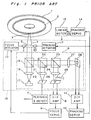
- FIG. 1 A prior art optical recording and playback device is shown in Fig. 1, which uses an optical disk 1 on which data recording/playback track 2 is formed.
- the light beam 4 emitted by the laser diode 17 is converted to a parallel beam by a collimator lens 18, passed through a half mirror 19, and focused to a spot 3 by an objective lens 5 on the optical disk 1.
- the light reflected from the optical disk 1 passes the objective lens 5 and is partially reflected by the half mirror 19 to the half mirror 20, which splits the beam in two.
- the reflected light from the half mirror 20 passes the coupling lens 21 and is converted to an electrical data read signal by the photodetector 22 and which is applied to the playback signal detector 7.
- the light which passes through the half mirror 20 is again split by another half mirror 23.
- the light reflected by the half mirror 23 passes the coupling lens 24 and is partially blocked by knife edge 25; the unblocked part is incident upon 1/2 divided photodetector 26, and an electrical focus error signal is detected by a differential amplifier 8.
- Phase compensation and other processing is applied to the focus error signal by the focus servo circuit 9, and the light beam 4 is focused on the recording medium surface of the optical disk 1 by moving the objective lens 5 in a roughly vertical perpendicular direction to the optical disk 1 surface by means of the focus actuator 10 according to the output of the focus servo circuit 9.
- the light passing through the half mirror 23 passes the coupling lens 27 and is incident upon the 1/2 divided photodetector 28, and is converted to an electrical tracking error signal by the differential amplifier 11.
- Phase compensation and other processing is applied to the tracking error signal by the tracking servo circuit 12, and the spot 3 is tracked along the data recording/playback track 2 by moving the objective lens 5 laterally in an approximately perpendicular direction to the track 2, i.e., perpendicular direction to the sheet when viewed in Fig. 1, by means of tracking actuator 13 based on the output of the tracking servo circuit 12.
- the output of the tracking servo circuit 12 is also input to the traverse servo circuit 14, which applies phase compensation and other processing before outputting the signal.
- the traverse servo circuit 14 is used to drive the linear motor 15 to move the optical head 6 fixed to the transport block 16, the focus actuator 10, and the tracking actuator 13 in a roughly laterally perpendicular direction to the signal recording/playback track 2, as effected when jumping a number of tracks.
- a light beam generated by a semiconductor laser or similar light source is focused on a disk-shaped recording medium rotating at a predetermined velocity to record and playback a signal thereon.
- This recording medium typically has a spiral recording track or concentric recording tracks approximately 1.2 ⁇ m wide at an approximately 1.6 ⁇ m pitch.
- a focusing servo focuses the light beam to a microscopic light spot with a maximum 1 ⁇ m diameter on the disk surface
- a tracking servo causes the light spot to track the signal track
- a traverse servo moves the optical head in a direction approximately perpendicular to the signal track.
- This prior art device differs from the above prior art device in the provision of a servo error signal detector which detects the deviation of the light beam from the control target position and converges the deviation into an electric signal to be outputted, an external disturbance generator which generates an external disturbance signal in a given characteristic, an adder which adds the external disturbance signal to the servo error signal from the servo error signal detector, and a servo circuit which corrects the phase and amplyfies the output signal from the adder.
- the servo error signal detector, the servo circuit and the actuator carry out the focus servo to focus the light beam to the recording medium on the optical disc and the tracking servo to trace the light beam to the track of the signal recording and reproducing.
- the output signals from the servo error signal detector and the adder are inputted to first and second band pass filters.
- the band pass filters which have the same frequency characteristics filter the frequency component of the given frequency of the external disturbance signal included in the output signals from the servo signal detector and the adder, respectively.
- a gain calculator which detects the amplitudes of the output signals from the band pass filters and obtains the gain at the given frequency in the servo loop by calculating the ratio (output amplitude of the first band pass filter)/(output amplitude of the second band pass filter), and a gain adjuster which manages the servo circuit to make the gain at the servo circuit a given value in accordance with the output signal from the gain calculator.
- the adjustment of the gain at the servo circuit results in the adjustment of the gain at the servo loop.
- this conventional optical recording and playback device is required to be provided with band pass filters in a narrow frequency band and a high accuracy in order to detect accurately the servo gain.
- an object of the present invention is to provide an optical recording and playback device in a small scale circuit capable of adjusting, at a high speed and at a high accuracy, the phase and gain characteristics of the servo loop.
- an optical recording and playback device for irradiating a light beam spot on a track of a data carrying medium comprising:
- a sine wave, single frequency reference signal is applied to the servo loop by the reference signal generator, the complex amplitude of the reference signal applied to the servo loop is detected by the detector for the complex amplitude of the signal ; the servo loop phase and gain characteristics are calculated from the output of the complex amplitude detection means and the complex amplitude of the previously stored reference signal applied to the servo loop, and a command is applied to the phase/gain adjustment means by the control means according to the operator output to set the servo loop phase and gain characteristics to the predetermined values.
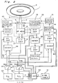
- FIG. 2 a block diagram of an optical recording and playback device according to a preferred embodiment of the present invention is shown, wherein a digital signal processor (hereinafter DSP) is used for the control means.
- DSP digital signal processor
- the optical recording and playback device comprises an optical disk 1, signal recording/playback track 2, optical spot 3, light beam 4, objective lens 5, optical head 6, differential amplifier 8, differential amplifier 11, focus actuator 10, tracking actuator 13, linear motor 15, and transport block 16, each said component being the same as those in the prior art optical recording and playback device described above.
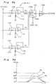
- a circuit diagram of an example of differential amplifier 8 is shown in Fig. 3, wherein reference number 100 is an operational amplifier and 101, 102, 103, and 104 are resistors.
- the optical recording and playback device also comprises a digital signal processor 30, sine wave data table 31, A/D convertor 32 and D/A convertor 33, a switch 34 to switch the input to the A/D convertor 32 as controlled by the DSP 30, a switch 35 to switch the output from the D/A convertor 33 as controlled by the DSP 30, an adder 36 for adding the output from differential amplifier 8 and the output from switch 35, an adder 39 for adding the output from differential amplifier 11 and the output from switch 35, and an adder 42 for adding the output from tracking servo circuit 41 and the output from switch 35.
- the variable gain amplifiers 37, 40 and 43 change the gain level as controlled by the DSP 30.
- An example of the variable gain amplifier 37 is shown in Fig. 4.
- This variable gain amplifier uses a multiplying type D/A convertor 110, which employs ladder resistors and a switch.
- a signal input to the reference input of the D/A convertor 110 is varied in response to the digital data applied to convertor 110 from DSP 30 such that, for example, when a digital data indicative of 5 is applied to D/A 110 from DSP 30, the reference input signal is amplified by 5 times, and similarly when a digital data indicative of 10 is applied to D/A 110 from DSP 30, the reference input signal is amplified by 10 times.
- the focusing servo circuit 38 and the tracking servo circuit 41 both switch the phase characteristics according to DSP 30 control, and each have a basically equivalent circuit design.
- An example of the focusing servo circuit 38 and tracking servo circuit 41 is shown in Fig. 5a which is a type that can present three different phase characteristics, such as shown by curves Pa, Pb and Pc in Fig. 5b. As shown in Fig.
- the servo circuit comprises operational amplifiers 111, 115 and 119, resistors 112, 113, 116, 117, 120 and 121, capacitors 114, 118 and 122, and a switch 123 which switches the input to the power amplifier 109 between operational amplifier 111, operational amplifier 115, and operational amplifier 119 as controlled by the DSP 30.
- the servo circuit comprises three phase compensation circuits: one formed by operational amplifier 111, resistors 112 and 113, and capacitor 114; one by operational amplifier 115, resistors 116 and 117, and capacitor 118; and one by operational amplifier 119, resistors 120 and 121, and capacitor 122.
- the three phase compensation circuits have the same gain but different phase characteristics at the gain crossover frequency f0 of the servo loop.
- a signal having a phase characteristics Pa shown in Fig. 5b is produced so that the phase difference of 50° is obtained at the gain crossover frequency f0.
- a signal having a phase characteristics Pb or Pc shown in Fig. 5b is produced so that the phase difference of 40° or 30° is obtained at the gain crossover frequency f0.
- phase difference of about 40°-50° at the gain crossover frequency f0, so that when a phase is detected as having a degree smaller than the required degree, e.g., 40°, DSP 30 selects terminal 123a to increase the phase difference. On the other hand, when the detected phase is greater than the required degree 50°, DSP selects terminal 123c to decrease the phase difference.
- the traverse servo loop 44 switches the phase characteristics as controlled by the DSP 30.
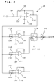
- An example of the traverse servo loop 44 is shown in Fig. 6.
- the traverse servo circuit shown in Fig. 6 switches between three types of circuit phase characteristics, in a similar manner to that shown in Fig. 5b.
- the servo circuit 44 comprises operational amplifiers 130, 135, 139, and 143, resistors 131, 132, 136, 137, 140, 141, 144 and 145, capacitors 133, 134, 138, 142, and 146, and a switch 147 which switches the input to the power amplifier 148 between operational amplifiers 135, 139, and 143 as controlled by the DSP 30.
- the servo circuit comprises three phase compensation circuits: one formed by operational amplifier 135, resistors 136 and 137, and capacitor 138; one by operational amplifier 139, resistors 140 and 141, and capacitor 142; and one by operational amplifier 143, resistors 144 and 145, and capacitor 146.
- the three phase compensation circuits have the same gain but different phase characteristics at the gain crossover frequency f0 of the servo loop.
- the circuit formed by the operational amplifier 130, resistors 131 and 132, and capacitors 133 and 134 has frequency characteristics approximately equal to those of the tracking actuator, and estimates the displacement from the midpoint of the tracking actuator.
- An optical recording and playback device constructed as described above operates as follows.
- a servo control system generally includes an adder AD and an operating arrangement GS.
- a focus servo system defined by elements 37, 38, 10, 8, 5 and 6 for the focus servo arrangement and adder 36
- a tracking servo system defined by elements 40, 41, 13, 11, 5 and 6 for the tracking servo arrangement and adder 39
- a traverse servo system defined by elements 43, 44, 15 and 16 for the traverse servo arrangement and adder 42.
- Each servo arrangement has its input A and output B, and also each servo system has its input X and output Y, wherein X and Y are complex numbers. The description hereinbelow is particularly directed to the focus servo system, but is applicable to the other two servo systems.
- the servo system of the present invention controls the gain of servo loop by changing the gain in the variable gain amplifier 37 to maintain the crossover frequency at f0 at which 0dB gain is obtained.
- the servo system of the present invention automatically returns the gain characteristics to the desired characteristics g1. For example, when the gain characteristics deviates from g1 to g2, the gain of the servo loop is decreased by variable gain amplifier 37 to return the gain characteristics to g1. In other words, the crossover frequency at which the 0dB gain is obtained is shifted from f2 to f0.
- the gain of the servo loop is increased by variable gain amplifier 37 to return the gain characteristics to g1.
- the crossover frequency at which the 0dB gain is obtained is shifted from f3 to f0.
- the phase difference dP may be change to be greater or smaller than the preferable range 40°-50°.
- the focus servo circuit 38 is also activated to change the phase characteristics, as shown in Fig. 5b, in a manner described above.
- the focusing servo, tracking servo, and traverse servo are made operative (step S1). Then, by the control of DSP 30, the switch 34 is turned to output 34a which is connected to the output of the differential amplifier 8, and the switch 35 is turned to output 35a which is connected to the adder 36 (step S2).
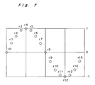
- the memory Acr in DSP 30 for storing the real part of output Y (Fig. 8a) and the memory Ari in DSP 30 for storing the imaginary part of output Y are reset to zero, and also address counter n for counting the r n in the sine table 31 shown in Fig. 7 is reset to zero, so as to be ready for start counting a sine wave.
- the DSP 30 reads the numeric data for the sine wave from the sine wave data table 31.
- the sine wave data table 31 may be formed by a ROM or RAM device.
- the DSP 30 sequentially reads the sine wave data table 31 at a constant time interval, and a D/A convertor 33 generates an analog signal from the read data to generate the sine wave signal r n ⁇ kf, wherein kf is a constant (step S4).
- the sine wave signal r n ⁇ kf is used as the input X (Fig. 8a) which is applied to adder 36.
- the DSP 30 then waits a predetermined time Ts before reading the next data r1 from the sine wave data table 31.
- the DSP 30 reads the focus error signal d1 digitally converted by the A/D convertor 32, multiplies this signal by the r1 read from the sine wave data table 31, adds the result d1 ⁇ r1 to the memory Aci which then adds the new result d1 ⁇ r1 to old results d0 ⁇ r0 so far added.
- the DSP 30 multiplies the focus error signal d1 by the r5 value read from the sine wave data table 31, adds the result d1 ⁇ r5 to the value already stored in memory Acr.
- step S7 The above operation is thereafter repeated while advancing the respective addresses r2, r3, to complete one sine waveform and r6, r7, to complete one cosine waveform.
- Such a calculation using one complete sine wave or one complete cosine wave is repeated K times (step S7) to accumulate data in memories Acr and Aci.
- a complex amplitude of the frequency component of the reference signal in the focus error signal can be obtained by dividing the data accumulated after K cycles of the sine wave by (N x K ö 2).
- the DSP 30 obtains G0/G and applies the result to the variable gain amplifier 37 to adjust the servo loop gain to the desired value (step S8).
- the DSP 30 applies a command to the focusing servo circuit 38 to change the servo loop phase characteristics to the phase compensation circuit with a greater phase advance, such as from terminal 123b to terminal 123a, when the measured phase advance is less than the specified value, to the phase compensation circuit with a smaller phase advance, such as from terminal 123b to terminal 123c, when the measured phase advance is greater than the specified value, and to hold the present phase compensation circuit when the measured phase advance is approximately equal to the specified value, thus adjusting the phase characteristics of the servo loop to approximately the specified value (step S9).
- a greater phase advance such as from terminal 123b to terminal 123a
- the phase compensation circuit with a smaller phase advance such as from terminal 123b to terminal 123c
- phase characteristics can also be switched by determining the shift in the phase characteristics of the servo loop directly from the Gi/Gr value without calculating tan ⁇ 1.
- the gain and phase characteristics of the tracking servo loop can also be adjusted with the same operation as that of the focusing servo adjustment by the switch 34 being turned to terminal 34b for the connection to the differential amplifier 11 and the switch 35 being turned to terminal 35b for the connection to the adder 39, as controlled by the DSP 30.
- the sine wave data table may be the same as that used for focus servo adjustment, or a different one may be used. Furthermore, by changing the time interval Ts at which data is read from the table, a reference signal with a frequency different from that used in focus servo adjustment can be obtained. The frequency can also be changed by outputting the values of the sine wave data table 31 in a non-consecutive sequence, or by outputting the same sine wave data table 31 data plural times. In addition, the coefficient kf and repeat K values may also differ from those used during focus servo adjustment.
- step S11 the focusing servo, tracking servo, and traverse servo are made operative.
- the switch 34 is turned to terminal 34c for connection with the output of the tracking servo circuit 41 and the switch 35 is turned to terminal 35c for connection with the adder 42, based on DSP 30 control (step S12).
- various parameters are reset (step S13).
- the DSP 30 reads the numeric data for the sine wave from the sine wave data table 31 in sequence from r0, multiplies the data by a predetermined coefficient kf and a D/A convertor converts the signal to an analog signal which is output as the reference signal.
- the reference signal is added to the tracking drive signal, which is the output of the tracking servo circuit 41, by the adder 42.
- the DSP 30 reads the tracking drive signal d0 converted to a digital signal by the A/D convertor 32, multiplies this signal by the r0 read from the sine wave data table 31 and writes the value to memory Aci.
- the DSP 30 multiplies the r4 read from the sine wave data table 31 by the read tracking drive signal d0, and writes the result to memory Acr.
- the DSP 30 then waits a predetermined time Ts before re-reading the data r0 from the sine wave data table 31.
- the data is converted to an analog signal by the D/A convertor and added to the tracking drive signal.
- the DSP 30 reads the tracking drive signal d1 digitally converted by the A/D convertor 32, multiplies this signal by the r0 value read from the sine wave data table 31, adds the result to the value stored to memory Aci, and thereafter the value is accumulated in memory Aci.
- the DSP 30 multiplies the tracking drive signal d1 by the r4 read from the sine wave data table 31, adds the result to the value stored to memory Acr, and thereafter the value is accumulated in memory Acr.
- the value read from the sine wave data table 31 is advanced by one, and the same calculations are performed using the values r1 and r5.
- the complex amplitude of the frequency component of the reference signal in the tracking drive signal can be obtained by dividing the data accumulated after K cycles of the sine wave by (N ⁇ K ⁇ M ö 2).
- the frequency of the reference signal at this time is 1/M the reference frequency during focus servo and tracking servo adjustment. This frequency approximates the frequency at which the tracking actuator gain and the traverse servo gain are equal.
- the traverse servo characteristics can be adjusted by performing the same calculations and adjustments from the detected complex amplitude as during focus servo and tracking servo adjustment.
- sine wave data table is used for focus servo and tracking servo adjustment and for traverse servo adjustment, but a distinct sine wave data table can also be used for traverse servo adjustment.
- the stability of the servo loop is determined by the frequency characteristics near the gain crossover, it is important to obtain the frequency characteristics near the gain crossover. It is therefore effective to use, as the frequency for characteristics measurement, a frequency near the gain crossover where there is little disk address or other noise. Furthermore, because the loop gain is approximately 1 if the frequency of the reference signal is a frequency near the gain crossover frequency of the servo loop, the precision of the gain calculation and complex amplitude detection of the signal can be increased.
- Standard 86 mm optomagnetic disks have a calibration zone on the inside and outside circumferences, and these zones may also be used for adjustments because the characteristics thereof are typical of the read/write area of the disk.
- the gain can be measured in the high density track at the inside circumference of the disk and stored as a value typical of the read-only area, and the gain measured in the calibration zone can be stored as the characteristic typical of the read/write area of the disk, and these values be selectively used in the read/write and read-only areas of the disk.
- the reference signal applied to the servo loop may be placed within the servo circuit or after the servo circuit. Furthermore, by storing the characteristics between the point where the reference signal is added and the point where the complex amplitude of the reference signal added in the servo loop is measured, the characteristics of the servo loop can be obtained by calculation insofar as the point where the complex amplitude of the signal is measured is in the servo loop.
- the sine wave data table can be obtained by storing values for only a 1/2 or 1/4 cycle of the sine wave signal, and the one cycle signal can be obtained from these divisions through calculation. For example, if the values for the first 1/2 cycle are stored, the signals can be output without modification for the first 1/2 cycle of the signal, and the signals for the second half cycle can be obtained by multiplying the first 1/2 cycle values by -1, thus making it possible to output values for one full sine wave cycle.
- the values for the first 1/4 cycle of the sine wave are stored, the values for the first 1/4 cycle can be output without modification, the values for the next 1/4 cycle can be inverted and output for the corresponding address in the next 1/4 cycle, and the values for the second 1/2 of the cycle can be obtained by multiplying the values for the first 1/2 cycle by -1, thus making it possible to output values for one full sine wave cycle while storing the values for only 1/4 cycle.
- a constant gain detection precision can be obtained by calculating the complex amplitude each time the reference signal is output one full cycle, obtaining the distribution of the complex amplitude of the reference signal in the detected servo loop, and measuring until the distribution divided by N is less than a preset value when the number of the detected complex amplitudes is N.
- the sinusoidal waveform signal generator 31 generates a sinusoidal waveform having a frequency at approximately the same as a gain crossover frequency of the servo loop.
- the sinusoidal waveform signal generator 31 generates a sine waveform and cosine waveform for use in the orthogonal phase heterodyne detection.
- the frequency of the sinusoidal waveform signal for reference signal is varied by changing the data table read time.
- the frequency of the sinusoidal waveform signal for reference signal is varied by changing the number of times the same data is read from the data table.
- the gain characteristics (G) and the servo loop phase are calculated in DSP 30 at the time the disk is loaded, and preferably every after a predetermined time interval repeatedly until the distribution of the detected signal complex amplitude is reduced lower than a predetermined value.
- the gain characteristics (G) and the servo loop phase are calculated during the light beam spot irradiating at the disk read/write area and at the disk area where data is pre-recorded with a pit-land signal.
- the reference signal is executed for multiple of one full cycle of a single frequency reference signal.
- the servo circuits may also be formed by a digital filter using, e.g., a DSP.
- the gain and phase characteristics in this case can be set by changing the coefficient of the digital filter.
- a RAM having a same size as that used for the reference signal table, for periodically accumulating and storing the data read from the A/D converter so that after the data accumulation of M cycles (M being an integer) of the reference signal, the complex amplitude of the signal is calculated using the values from the reference signal table to calculate the complex amplitude of the signal.
- an optical recording and playback device can automatically measure the servo loop gain and phase characteristics, and can achieve stable servo characteristics by adjusting the servo loop gain and phase characteristics to preset values.
Landscapes
- Optical Recording Or Reproduction (AREA)
- Moving Of The Head To Find And Align With The Track (AREA)
Description
- The present invention relates to an optical recording and playback device which records and reads code information, audio and video information using an optical read/writable medium by means of a semiconductor laser or other light source.
- A prior art optical recording and playback device is shown in Fig. 1, which uses an
optical disk 1 on which data recording/playback track 2 is formed. Thelight beam 4 emitted by the laser diode 17 is converted to a parallel beam by acollimator lens 18, passed through a half mirror 19, and focused to aspot 3 by anobjective lens 5 on theoptical disk 1. The light reflected from theoptical disk 1 passes theobjective lens 5 and is partially reflected by the half mirror 19 to thehalf mirror 20, which splits the beam in two. The reflected light from thehalf mirror 20 passes thecoupling lens 21 and is converted to an electrical data read signal by thephotodetector 22 and which is applied to theplayback signal detector 7. The light which passes through thehalf mirror 20 is again split by anotherhalf mirror 23. - The light reflected by the
half mirror 23 passes thecoupling lens 24 and is partially blocked byknife edge 25; the unblocked part is incident upon 1/2 dividedphotodetector 26, and an electrical focus error signal is detected by adifferential amplifier 8. Phase compensation and other processing is applied to the focus error signal by thefocus servo circuit 9, and thelight beam 4 is focused on the recording medium surface of theoptical disk 1 by moving theobjective lens 5 in a roughly vertical perpendicular direction to theoptical disk 1 surface by means of thefocus actuator 10 according to the output of thefocus servo circuit 9. - The light passing through the
half mirror 23 passes thecoupling lens 27 and is incident upon the 1/2 dividedphotodetector 28, and is converted to an electrical tracking error signal by the differential amplifier 11. Phase compensation and other processing is applied to the tracking error signal by thetracking servo circuit 12, and thespot 3 is tracked along the data recording/playback track 2 by moving theobjective lens 5 laterally in an approximately perpendicular direction to thetrack 2, i.e., perpendicular direction to the sheet when viewed in Fig. 1, by means of trackingactuator 13 based on the output of thetracking servo circuit 12. - The output of the
tracking servo circuit 12 is also input to thetraverse servo circuit 14, which applies phase compensation and other processing before outputting the signal. Thetraverse servo circuit 14 is used to drive thelinear motor 15 to move theoptical head 6 fixed to thetransport block 16, thefocus actuator 10, and thetracking actuator 13 in a roughly laterally perpendicular direction to the signal recording/playback track 2, as effected when jumping a number of tracks. - In the prior art optical recording and playback device, a light beam generated by a semiconductor laser or similar light source is focused on a disk-shaped recording medium rotating at a predetermined velocity to record and playback a signal thereon. This recording medium typically has a spiral recording track or concentric recording tracks approximately 1.2 µm wide at an approximately 1.6 µm pitch. To record a signal to this track or read a recorded signal back from this track, a focusing servo focuses the light beam to a microscopic light spot with a maximum 1 µm diameter on the disk surface, a tracking servo causes the light spot to track the signal track, and a traverse servo moves the optical head in a direction approximately perpendicular to the signal track.
- It is known a further conventional optical recording and playback device defining the closest prior art from which the invention proceeds. This prior art device differs from the above prior art device in the provision of a servo error signal detector which detects the deviation of the light beam from the control target position and converges the deviation into an electric signal to be outputted, an external disturbance generator which generates an external disturbance signal in a given characteristic, an adder which adds the external disturbance signal to the servo error signal from the servo error signal detector, and a servo circuit which corrects the phase and amplyfies the output signal from the adder. The servo error signal detector, the servo circuit and the actuator carry out the focus servo to focus the light beam to the recording medium on the optical disc and the tracking servo to trace the light beam to the track of the signal recording and reproducing. The output signals from the servo error signal detector and the adder are inputted to first and second band pass filters. The band pass filters which have the same frequency characteristics filter the frequency component of the given frequency of the external disturbance signal included in the output signals from the servo signal detector and the adder, respectively. Furthermore, there are provided a gain calculator which detects the amplitudes of the output signals from the band pass filters and obtains the gain at the given frequency in the servo loop by calculating the ratio (output amplitude of the first band pass filter)/(output amplitude of the second band pass filter), and a gain adjuster which manages the servo circuit to make the gain at the servo circuit a given value in accordance with the output signal from the gain calculator. In such a way, the adjustment of the gain at the servo circuit results in the adjustment of the gain at the servo loop. However, this conventional optical recording and playback device is required to be provided with band pass filters in a narrow frequency band and a high accuracy in order to detect accurately the servo gain.
- Therefore, an object of the present invention is to provide an optical recording and playback device in a small scale circuit capable of adjusting, at a high speed and at a high accuracy, the phase and gain characteristics of the servo loop.
- To achieve the aforementioned object, in accordance with the present invention there is provided an optical recording and playback device for irradiating a light beam spot on a track of a data carrying medium comprising:
- a deviation detection means for outputting a signal representing the deviation of the light beam spot from a servo control target position;
- servo control means defining a closed servo loop with said deviation detection means for moving said light beam spot to and holding it at said servo control target position; and
- a reference signal generator for generating an external reference signal containing a predetermined frequency component and applying it to said servo loop;
- characterized in that said optical recording and playback device further comprises:
- means for calculating the real part and imaginary part of the complex number representation of said predetermined frequency component contained in the deviation signal as detected by said deviation detection means in relation to the predetermined frequency component applied to the servo loop ;
- means for calculating the gain characteristics and phase characteristics of the servo loop from the real and imaginary parts of said calculated complex number, and the real and imaginary parts of the complex number of said predetermined frequency component contained in the external reference signal which are preliminarily stored; and
- adjustment means inserted into said servo loop for changing the gain characteristics of said servo loop in response to the calculated gain characteristics.
- Further advantageous embodiments are defined in the sub-claims.
- In the servo assembly of an optical recording and playback device constructed as described above, while driving the servos based on the servo error signal detected by the servo error signal detector, a sine wave, single frequency reference signal is applied to the servo loop by the reference signal generator, the complex amplitude of the reference signal applied to the servo loop is detected by the detector for the complex amplitude of the signal ; the servo loop phase and gain characteristics are calculated from the output of the complex amplitude detection means and the complex amplitude of the previously stored reference signal applied to the servo loop, and a command is applied to the phase/gain adjustment means by the control means according to the operator output to set the servo loop phase and gain characteristics to the predetermined values.
- The present invention will become more fully understood from the detailed description given below and the accompanying diagrams wherein:
- Fig. 1 is a block diagram of a prior art optical recording and playback device;
- Fig. 2 is a block diagram of an optical recording and playback device according to a preferred embodiment of the present invention;
- Fig. 3 is a circuit diagram of a differential circuit employed in the circuit of Fig. 2;
- Fig. 4 is a circuit diagram of a variable gain amplifier employed in the circuit of Fig. 2;
- Fig. 5a is a circuit diagram of a basic focusing servo circuit and a tracking servo circuit employed in the circuit of Fig. 2;
- Fig. 5b is a graph showing different phase signals produced from the circuit of Fig. 5a;
- Fig. 6 is a circuit diagram of a traverse servo circuit employed in the circuit of Fig. 2;
- Fig. 7 is a graph showing a data array in a sine wave data table employed in the circuit of Fig. 2;
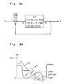
- Fig. 8a is a diagram of servo system of the circuit of Fig. 2;
- Fig. 8b is a graph showing gain characteristics and phase characteristics of the servo system;
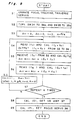
- Fig. 9 is a flow chart showing an operation of the focusing servo and tracking servo; and
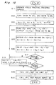
- Fig. 10 is a flow chart showing an operation of the traverse servo.
- Referring to Fig. 2 a block diagram of an optical recording and playback device according to a preferred embodiment of the present invention is shown, wherein a digital signal processor (hereinafter DSP) is used for the control means. As shown in Fig. 2, the optical recording and playback device comprises an
optical disk 1, signal recording/playback track 2,optical spot 3,light beam 4,objective lens 5,optical head 6,differential amplifier 8, differential amplifier 11,focus actuator 10,tracking actuator 13,linear motor 15, andtransport block 16, each said component being the same as those in the prior art optical recording and playback device described above. A circuit diagram of an example ofdifferential amplifier 8 is shown in Fig. 3, whereinreference number 100 is an operational amplifier and 101, 102, 103, and 104 are resistors. - As shown in Fig. 2, the optical recording and playback device also comprises a
digital signal processor 30, sine wave data table 31, A/D convertor 32 and D/A convertor 33, aswitch 34 to switch the input to the A/D convertor 32 as controlled by theDSP 30, aswitch 35 to switch the output from the D/A convertor 33 as controlled by theDSP 30, anadder 36 for adding the output fromdifferential amplifier 8 and the output fromswitch 35, anadder 39 for adding the output from differential amplifier 11 and the output fromswitch 35, and anadder 42 for adding the output from trackingservo circuit 41 and the output fromswitch 35. The variable gain amplifiers 37, 40 and 43 change the gain level as controlled by theDSP 30. An example of thevariable gain amplifier 37 is shown in Fig. 4. This variable gain amplifier uses a multiplying type D/A convertor 110, which employs ladder resistors and a switch. A signal input to the reference input of the D/A convertor 110 is varied in response to the digital data applied toconvertor 110 fromDSP 30 such that, for example, when a digital data indicative of 5 is applied to D/A 110 fromDSP 30, the reference input signal is amplified by 5 times, and similarly when a digital data indicative of 10 is applied to D/A 110 fromDSP 30, the reference input signal is amplified by 10 times. - The focusing
servo circuit 38 and the trackingservo circuit 41 both switch the phase characteristics according toDSP 30 control, and each have a basically equivalent circuit design. An example of the focusingservo circuit 38 and trackingservo circuit 41 is shown in Fig. 5a which is a type that can present three different phase characteristics, such as shown by curves Pa, Pb and Pc in Fig. 5b. As shown in Fig. 5a, the servo circuit comprisesoperational amplifiers resistors capacitors switch 123 which switches the input to thepower amplifier 109 between operational amplifier 111,operational amplifier 115, andoperational amplifier 119 as controlled by theDSP 30. The servo circuit comprises three phase compensation circuits: one formed by operational amplifier 111,resistors capacitor 114; one byoperational amplifier 115,resistors capacitor 118; and one byoperational amplifier 119,resistors capacitor 122. The three phase compensation circuits have the same gain but different phase characteristics at the gain crossover frequency f₀ of the servo loop. Thus, when terminal 123a is selected byDSP 30, a signal having a phase characteristics Pa shown in Fig. 5b is produced so that the phase difference of 50° is obtained at the gain crossover frequency f₀. Similarly, whenterminals DSP 30, a signal having a phase characteristics Pb or Pc shown in Fig. 5b is produced so that the phase difference of 40° or 30° is obtained at the gain crossover frequency f₀. It is preferable to have a phase difference of about 40°-50° at the gain crossover frequency f₀, so that when a phase is detected as having a degree smaller than the required degree, e.g., 40°,DSP 30 selects terminal 123a to increase the phase difference. On the other hand, when the detected phase is greater than the required degree 50°, DSP selects terminal 123c to decrease the phase difference. - The
traverse servo loop 44 switches the phase characteristics as controlled by theDSP 30. An example of thetraverse servo loop 44 is shown in Fig. 6. The traverse servo circuit shown in Fig. 6 switches between three types of circuit phase characteristics, in a similar manner to that shown in Fig. 5b. As shown in Fig. 6, theservo circuit 44 comprisesoperational amplifiers resistors capacitors switch 147 which switches the input to thepower amplifier 148 betweenoperational amplifiers DSP 30. The servo circuit comprises three phase compensation circuits: one formed byoperational amplifier 135,resistors capacitor 138; one byoperational amplifier 139,resistors capacitor 142; and one byoperational amplifier 143,resistors capacitor 146. The three phase compensation circuits have the same gain but different phase characteristics at the gain crossover frequency f₀ of the servo loop. The circuit formed by theoperational amplifier 130,resistors capacitors - An optical recording and playback device according to the preferred embodiment of the present invention constructed as described above operates as follows.
- As shown in Fig. 8a, a servo control system generally includes an adder AD and an operating arrangement GS. In the circuit of Fig. 2, there are three servo control systems: a focus servo system defined by
elements adder 36; a tracking servo system defined byelements adder 39; and a traverse servo system defined byelements adder 42. Each servo arrangement has its input A and output B, and also each servo system has its input X and output Y, wherein X and Y are complex numbers. The description hereinbelow is particularly directed to the focus servo system, but is applicable to the other two servo systems. - The aim of the focus servo system according to the present invention is to maintain the gain G of the focus servo arrangement to be equal to 1 with a crossover frequency being fixed at f₀, as indicated below,


variable gain amplifier 37 to maintain the crossover frequency at f₀ at which 0dB gain is obtained. - When the gain characteristics deviates from a desired characteristics, such as shown by line gl in Fig. 8b, to undesired characteristics, such as shown by line g2 or g3, due to the temperature change and/or variation in the constructing parts, the servo system of the present invention automatically returns the gain characteristics to the desired characteristics g1. For example, when the gain characteristics deviates from g1 to g2, the gain of the servo loop is decreased by
variable gain amplifier 37 to return the gain characteristics to g1. In other words, the crossover frequency at which the 0dB gain is obtained is shifted from f₂ to f₀. On the other hand, when the gain characteristics deviates from g1 to g3, the gain of the servo loop is increased byvariable gain amplifier 37 to return the gain characteristics to g1. In other words, the crossover frequency at which the 0dB gain is obtained is shifted from f₃ to f₀. - When the gain characteristic line is changed, e.g., from gl to g2, the phase difference dP may be change to be greater or smaller than the
preferable range 40°-50°. In such a case, according to the present invention, thefocus servo circuit 38 is also activated to change the phase characteristics, as shown in Fig. 5b, in a manner described above. - The focusing servo characteristics adjustment operation is further described with reference to the flow chart shown in Fig. 9.
- First, the focusing servo, tracking servo, and traverse servo are made operative (step S1). Then, by the control of
DSP 30, theswitch 34 is turned tooutput 34a which is connected to the output of thedifferential amplifier 8, and theswitch 35 is turned tooutput 35a which is connected to the adder 36 (step S2). The memory Acr inDSP 30 for storing the real part of output Y (Fig. 8a) and the memory Ari inDSP 30 for storing the imaginary part of output Y are reset to zero, and also address counter n for counting the rn in the sine table 31 shown in Fig. 7 is reset to zero, so as to be ready for start counting a sine wave. Furthermore, m=N/4 is set, wherein N is the maximum of the address counter in the sine table of Fig. 7, so as to be ready for starting counting a cosine wave (step S3). - Then, the
DSP 30 reads the numeric data for the sine wave from the sine wave data table 31. The sine wave data table 31 may be formed by a ROM or RAM device. Fig. 7 is a chart of the data in a 16-point data sine wave data table 31 where the rn (n=0, 1, 2, ......, N) values are stored in the ROM or RAM device. TheDSP 30 sequentially reads the sine wave data table 31 at a constant time interval, and a D/A convertor 33 generates an analog signal from the read data to generate the sine wave signal rn·kf, wherein kf is a constant (step S4). The sine wave signal rn·kf is used as the input X (Fig. 8a) which is applied to adder 36. - In the first cycle operation, the
DSP 30 reads the data from the sine wave data table 31 in sequence from r₀, multiplies the data by a predetermined coefficient kf and a D/A convertor 33 converts the signal to an analog signal which is output as the reference signal X=r₀·kf. The reference signal X is added to the focus error signal-Y=d₀ to obtain r₀·kf+d₀. In the meantime, theDSP 30 reads the focus error signal-Y=d₀ which is converted to a digital signal by the A/D convertor 32. Then, inDSP 30, the focus error signal-Y=d₀ is multiplied by the r₀ read from the sine wave data table 31 and writes the value d₀·r₀ to memory Aci representing the imaginary part of-Y (step S5). Furthermore, theDSP 30 multiplies r₄ representing cosine as read from the sine wave data table 31 by the read focus error signal-Y=d₀, and writes the result d₀·r₄ to memory Acr representing the real part of-Y (step S6). If N is the number of data values for one complete sine wave cycle, then the cosine wave signal can be obtained by reading the sine wave data table 31 from a point which is offset N/4. - The
DSP 30 then waits a predetermined time Ts before reading the next data r₁ from the sine wave data table 31. This data is multiplied by the coefficient kf and is converted to an analog signal by the D/A convertor 33 and added to the focusing servo error signal-Y=d₁ to obtain r₁·kf+d₁. In the meantime, theDSP 30 reads the focus error signal d₁ digitally converted by the A/D convertor 32, multiplies this signal by the r₁ read from the sine wave data table 31, adds the result d₁·r₁ to the memory Aci which then adds the new result d₁·r₁ to old results d₀·r₀ so far added. Next, theDSP 30 multiplies the focus error signal d₁ by the r₅ value read from the sine wave data table 31, adds the result d₁·r₅ to the value already stored in memory Acr. - The above operation is thereafter repeated while advancing the respective addresses r2, r3, to complete one sine waveform and r6, r7, to complete one cosine waveform. Such a calculation using one complete sine wave or one complete cosine wave is repeated K times (step S7) to accumulate data in memories Acr and Aci.
- After the above operation, a complex amplitude of the frequency component of the reference signal in the focus error signal can be obtained by dividing the data accumulated after K cycles of the sine wave by (N x K ö 2).
- Thus, if the complex amplitude of the reference signal, which is the value of the sine wave data table 31 multiplied by a specific coefficient kf, is Xc, and the complex amplitude of the frequency component of the reference signal in the detected focus error signal is Yc, then the complex expression Gc of the servo loop gain in the frequency of the applied reference signal can be obtained using the equation:


- The gain G is obtained from the real number Gr and imaginary number Gi components of Gc using the equation

- To adjust the detected gain G to the preset gain GO, the
DSP 30 obtains G0/G and applies the result to thevariable gain amplifier 37 to adjust the servo loop gain to the desired value (step S8). - The phase P of the servo loop in the frequency of the applied reference signal is obtained by the
DSP 30 as
- To adjust detected phase P to the specified phase, the
DSP 30 applies a command to the focusingservo circuit 38 to change the servo loop phase characteristics to the phase compensation circuit with a greater phase advance, such as from terminal 123b to terminal 123a, when the measured phase advance is less than the specified value, to the phase compensation circuit with a smaller phase advance, such as from terminal 123b to terminal 123c, when the measured phase advance is greater than the specified value, and to hold the present phase compensation circuit when the measured phase advance is approximately equal to the specified value, thus adjusting the phase characteristics of the servo loop to approximately the specified value (step S9). - It is to be noted that the phase characteristics can also be switched by determining the shift in the phase characteristics of the servo loop directly from the Gi/Gr value without calculating tan⁻¹.
- The gain and phase characteristics of the tracking servo loop can also be adjusted with the same operation as that of the focusing servo adjustment by the
switch 34 being turned toterminal 34b for the connection to the differential amplifier 11 and theswitch 35 being turned toterminal 35b for the connection to theadder 39, as controlled by theDSP 30. - For adjustment of the tracking servo, the sine wave data table may be the same as that used for focus servo adjustment, or a different one may be used. Furthermore, by changing the time interval Ts at which data is read from the table, a reference signal with a frequency different from that used in focus servo adjustment can be obtained. The frequency can also be changed by outputting the values of the sine wave data table 31 in a non-consecutive sequence, or by outputting the same sine wave data table 31 data plural times. In addition, the coefficient kf and repeat K values may also differ from those used during focus servo adjustment.
- Next is described traverse servo adjustment in the preferred embodiment, in connection with Fig. 10.
- In operation, at first, the focusing servo, tracking servo, and traverse servo are made operative (step S11). Then, the
switch 34 is turned to terminal 34c for connection with the output of the trackingservo circuit 41 and theswitch 35 is turned to terminal 35c for connection with theadder 42, based onDSP 30 control (step S12). Then, various parameters are reset (step S13). - Then, the
DSP 30 reads the numeric data for the sine wave from the sine wave data table 31 in sequence from r₀, multiplies the data by a predetermined coefficient kf and a D/A convertor converts the signal to an analog signal which is output as the reference signal. The reference signal is added to the tracking drive signal, which is the output of the trackingservo circuit 41, by theadder 42. TheDSP 30 reads the tracking drive signal d₀ converted to a digital signal by the A/D convertor 32, multiplies this signal by the r₀ read from the sine wave data table 31 and writes the value to memory Aci. Next, theDSP 30 multiplies the r₄ read from the sine wave data table 31 by the read tracking drive signal d₀, and writes the result to memory Acr. - The
DSP 30 then waits a predetermined time Ts before re-reading the data r₀ from the sine wave data table 31. The data is converted to an analog signal by the D/A convertor and added to the tracking drive signal. TheDSP 30 reads the tracking drive signal d₁ digitally converted by the A/D convertor 32, multiplies this signal by the r₀ value read from the sine wave data table 31, adds the result to the value stored to memory Aci, and thereafter the value is accumulated in memory Aci. Next, theDSP 30 multiplies the tracking drive signal d₁ by the r4 read from the sine wave data table 31, adds the result to the value stored to memory Acr, and thereafter the value is accumulated in memory Acr. After repeating this sequence M times, the value read from the sine wave data table 31 is advanced by one, and the same calculations are performed using the values r₁ and r₅. - The above operation is thereafter repeated while advancing the respective addresses r₂, r₃, ...... and r₆, r₇, .... by one with each repetition until reaching r₁₅, after which the loop returns to r₀, performing the calculation K times the sine wave cycle while accumulating the data.
- In this case, if the number of data values read from the data table for one cycle is N and the number of times the same data is output is M, the complex amplitude of the frequency component of the reference signal in the tracking drive signal can be obtained by dividing the data accumulated after K cycles of the sine wave by (N × K × M ö 2). The frequency of the reference signal at this time is 1/M the reference frequency during focus servo and tracking servo adjustment. This frequency approximates the frequency at which the tracking actuator gain and the traverse servo gain are equal. The traverse servo characteristics can be adjusted by performing the same calculations and adjustments from the detected complex amplitude as during focus servo and tracking servo adjustment.
- In the above description, the same sine wave data table is used for focus servo and tracking servo adjustment and for traverse servo adjustment, but a distinct sine wave data table can also be used for traverse servo adjustment.
- It is to be noted that because the stability of the servo loop is determined by the frequency characteristics near the gain crossover, it is important to obtain the frequency characteristics near the gain crossover. It is therefore effective to use, as the frequency for characteristics measurement, a frequency near the gain crossover where there is little disk address or other noise. Furthermore, because the loop gain is approximately 1 if the frequency of the reference signal is a frequency near the gain crossover frequency of the servo loop, the precision of the gain calculation and complex amplitude detection of the signal can be increased.
- In addition, it is also possible to adjust only the gain in a servo circuit with low phase change, or to adjust only the phase characteristics in a servo circuit with low gain change.
- Furthermore, by adjusting the gain and phase characteristics when the disk is loaded, it is also possible to compensate for the detection characteristics when the detection characteristics of the servo error signal vary with the disk. In addition, by performing the adjustment at a regular time interval, it is also possible to compensate for changes in the actuator characteristics and detection characteristics of the servo error signal caused by temperature changes.
- Standard 86 mm optomagnetic disks have a calibration zone on the inside and outside circumferences, and these zones may also be used for adjustments because the characteristics thereof are typical of the read/write area of the disk. In addition, in a disk comprising a read/write area and a read-only area recorded with a pit and land signal, the gain can be measured in the high density track at the inside circumference of the disk and stored as a value typical of the read-only area, and the gain measured in the calibration zone can be stored as the characteristic typical of the read/write area of the disk, and these values be selectively used in the read/write and read-only areas of the disk.
- It is to be noted that so long as the reference signal applied to the servo loop is within the servo loop, it may be placed within the servo circuit or after the servo circuit. Furthermore, by storing the characteristics between the point where the reference signal is added and the point where the complex amplitude of the reference signal added in the servo loop is measured, the characteristics of the servo loop can be obtained by calculation insofar as the point where the complex amplitude of the signal is measured is in the servo loop.
- The sine wave data table can be obtained by storing values for only a 1/2 or 1/4 cycle of the sine wave signal, and the one cycle signal can be obtained from these divisions through calculation. For example, if the values for the first 1/2 cycle are stored, the signals can be output without modification for the first 1/2 cycle of the signal, and the signals for the second half cycle can be obtained by multiplying the first 1/2 cycle values by -1, thus making it possible to output values for one full sine wave cycle. In addition, if the values for the first 1/4 cycle of the sine wave are stored, the values for the first 1/4 cycle can be output without modification, the values for the next 1/4 cycle can be inverted and output for the corresponding address in the next 1/4 cycle, and the values for the second 1/2 of the cycle can be obtained by multiplying the values for the first 1/2 cycle by -1, thus making it possible to output values for one full sine wave cycle while storing the values for only 1/4 cycle.
- It is to be noted that a constant gain detection precision can be obtained by calculating the complex amplitude each time the reference signal is output one full cycle, obtaining the distribution of the complex amplitude of the reference signal in the detected servo loop, and measuring until the distribution divided by N is less than a preset value when the number of the detected complex amplitudes is N.
- According to the present invention, the sinusoidal
waveform signal generator 31 generates a sinusoidal waveform having a frequency at approximately the same as a gain crossover frequency of the servo loop. - Also, the sinusoidal
waveform signal generator 31 generates a sine waveform and cosine waveform for use in the orthogonal phase heterodyne detection. - Furthermore, the frequency of the sinusoidal waveform signal for reference signal is varied by changing the data table read time.
- Also, the frequency of the sinusoidal waveform signal for reference signal is varied by changing the number of times the same data is read from the data table.
- The gain characteristics (G) and the servo loop phase are calculated in
DSP 30 at the time the disk is loaded, and preferably every after a predetermined time interval repeatedly until the distribution of the detected signal complex amplitude is reduced lower than a predetermined value. - Furthermore, the gain characteristics (G) and the servo loop phase are calculated during the light beam spot irradiating at the disk read/write area and at the disk area where data is pre-recorded with a pit-land signal.
- Preferably, the reference signal is executed for multiple of one full cycle of a single frequency reference signal.
- It is to be noted that the servo circuits may also be formed by a digital filter using, e.g., a DSP. The gain and phase characteristics in this case can be set by changing the coefficient of the digital filter.
- It is also possible to further provide a RAM, having a same size as that used for the reference signal table, for periodically accumulating and storing the data read from the A/D converter so that after the data accumulation of M cycles (M being an integer) of the reference signal, the complex amplitude of the signal is calculated using the values from the reference signal table to calculate the complex amplitude of the signal.
- In this case, it is preferable to obtain an average of the complex amplitude from reference signals calculated a plurality of times at an interval with a predetermined variation so that the gain detection can be effected with the noise signal having a frequency close to the frequency of the reference signal being eliminated.
- As thus described hereinabove, an optical recording and playback device according to the present invention can automatically measure the servo loop gain and phase characteristics, and can achieve stable servo characteristics by adjusting the servo loop gain and phase characteristics to preset values.
Claims (16)
- An optical recording and playback device for irradiating a light beam spot on a track of a data carrying medium comprising:a deviation detection means (8, 11) for outputting a signal (di) representing the deviation of the light beam spot from a servo control target position;servo control means (38, 10; 5, 6; 41, 13) defining a closed servo loop with said deviation detection means (8, 11) for moving said light beam spot to and holding it at said servo control target position; anda reference signal generator (30, 31, 32, 33) for generating an external reference signal (kf.ri) containing a predetermined frequency component and applying it to said servo loop;characterized in that said optical recording and playback device further comprises:means (30) for calculating the real part and imaginary part of the complex number representation of said predetermined frequency component contained in the deviation signal (di) as detected by said deviation detection means (8, 11) in relation to the predetermined frequency component applied to the servo loop;means (30) for calculating the gain characteristics (G) and phase characteristics (P) of the servo loop from the real and imaginary parts of said calculated complex number, and the real and imaginary parts of the complex number of said predetermined frequency component contained in the external reference signal which are preliminarily stored; andadjustment means (37;40;43) inserted into said servo loop for changing the gain characteristics of said servo loop in response to the calculated gain characteristics (G).
- An optical recording and playback device as claimed in claim 1, further comprising:
adjustment means (38;41) inserted into said servo loop for changing the servo loop phase in response to the calculated phase characteristics (P). - An optical recording and playback device as claimed in claim 1, wherein said reference signal generator comprises a sinusoidal waveform signal generator (31) for generating a sinusoidal waveform having a frequency which is approximately the same as a gain crossover frequency of the servo loop.
- An optical recording and playback device as claimed in claim 3, wherein said sinusoidal waveform signal generator (31) is a memory table for memorizing one cycle pattern of a sine waveform.
- An optical recording and playback device as claimed in claim 3, wherein said sinusoidal waveform signal generator (31) is a memory table for memorizing one half cycle pattern of a sine waveform.
- An optical recording and playback device as claimed in claim 3, wherein said sinusoidal waveform signal generator (31) is a memory table for memorizing one fourth cycle pattern of a sine waveform.
- An optical recording and playback device as claimed in claim 3, wherein the frequency of said sinusoidal waveform signal is varied by changing the number of times the same data is read from the data table.
- An optical recording and playback device as claimed in claim 1, wherein said means (30) for calculating the gain characteristics (G) of the servo loop and said means (37;40;43) for adjusting the gain characteristics (G) of the servo loop are effected at the time the disk is loaded.
- An optical recording and playback device as claimed in claim 2, wherein said means (30) for calculating the servo loop phase and said means (38;41) for adjusting the servo loop phase are effected at the time the disk is loaded.
- An optical recording and playback device as claimed in claim 1, wherein said means (30) for calculating a gain characteristics (G) of the servo loop and said means (37;40;43) for adjusting a gain characteristics (G) of the servo loop are effected after every predetermined time interval.
- An optical recording and playback device as claimed in claim 2, wherein said means (30) for calculating the servo loop phase and said means (38) for adjusting the servo loop phase are effected after every predetermined time interval.
- An optical recording and playback device as claimed in claim 1, wherein said means (30) for calculating the gain characteristics (G) of the servo loop and said means (37;40;43) for adjusting the gain characteristics (G) of the servo loop are effected at the disk read/write area and at the disk area where data is pre-recorded with a pit-land signal.
- An optical recording and playback device as claimed in claim 2, wherein said means (30) for calculating the servo loop phase and said means (38;41) for adjusting the servo loop phase are effected at the disk read/write area and at the disk area where data is pre-recorded with a pit-land signal.
- An optical recording and playback device as claimed in claim 1, wherein said means (30) for calculating the gain characteristics (G) of the servo loop and said means (37;40;43) for adjusting the gain characteristics (G) of the servo loop are effected repeatedly until the distribution of the detected signal complex amplitude is reduced lower than a predetermined value.
- An optical recording and playback device as claimed in claim 2, wherein said means (30) for calculating the servo loop phase and said means (38;41) for adjusting the servo loop phase are effected repeatedly until the distribution of the detected signal complex amplitude is reduced lower than a predetermined value.
- An optical recording and playback device as claimed in claim 1, wherein said calculation means (30) carries out a complex amplitude calculation for multiple of one full cycle of a single frequency reference signal.
Applications Claiming Priority (2)
| Application Number | Priority Date | Filing Date | Title |
|---|---|---|---|
| JP2159034A JP2563648B2 (en) | 1990-06-18 | 1990-06-18 | Optical recording / reproducing device |
| JP159034/90 | 1990-06-18 |
Publications (3)
| Publication Number | Publication Date |
|---|---|
| EP0462561A2 EP0462561A2 (en) | 1991-12-27 |
| EP0462561A3 EP0462561A3 (en) | 1992-03-11 |
| EP0462561B1 true EP0462561B1 (en) | 1996-05-01 |
Family
ID=15684808
Family Applications (1)
| Application Number | Title | Priority Date | Filing Date |
|---|---|---|---|
| EP91109951A Expired - Lifetime EP0462561B1 (en) | 1990-06-18 | 1991-06-18 | Optical recording and playback device |
Country Status (5)
| Country | Link |
|---|---|
| US (1) | US5199015A (en) |
| EP (1) | EP0462561B1 (en) |
| JP (1) | JP2563648B2 (en) |
| KR (1) | KR940009244B1 (en) |
| DE (1) | DE69119144T2 (en) |
Cited By (4)
| Publication number | Priority date | Publication date | Assignee | Title |
|---|---|---|---|---|
| US5978331A (en) | 1995-12-06 | 1999-11-02 | Discovision Associates | Apparatus and method for focus control |
| US5978329A (en) | 1995-06-07 | 1999-11-02 | Discovision Associates | Technique for closed loop servo operation in optical disc tracking control |
| US6134199A (en) | 1996-04-01 | 2000-10-17 | Discovision Associates | Closed loop servo operation for focus control |
| US8937854B2 (en) | 2001-01-25 | 2015-01-20 | Optical Devices, Llc | Servo processor receiving photodetector signals |
Families Citing this family (13)
| Publication number | Priority date | Publication date | Assignee | Title |
|---|---|---|---|---|
| JPH0668498A (en) * | 1992-08-24 | 1994-03-11 | Toshiba Corp | Information recording medium processor |
| KR100230228B1 (en) * | 1993-07-31 | 1999-11-15 | 윤종용 | Focusing control device of optical disc system |
| US5436880A (en) * | 1994-01-10 | 1995-07-25 | Eastman Kodak Company | Laser power control in an optical recording system using partial correction of reflected signal error |
| EP0877373A4 (en) | 1996-01-22 | 1999-04-21 | Hitachi Ltd | Magnetic disk apparatus |
| US6407876B1 (en) | 1996-01-22 | 2002-06-18 | Hitachi, Ltd. | Magnetic disk apparatus having an accelerometer for detecting acceleration in the positioning direction of the magnetic head |
| US7196979B2 (en) * | 2001-01-25 | 2007-03-27 | Dphi Acquisitions, Inc. | Calibration storage methods for a digital focus and tracking servo system with calibration |
| US20070104050A1 (en) * | 2003-06-25 | 2007-05-10 | Matsushita Electric Industrial Co., Ltd | Focus control device and tracking control device |
| US7298674B2 (en) | 2003-11-17 | 2007-11-20 | Via Technologies, Inc. | Method and device for adjusting a control parameter of a servo of an optical drive |
| TWI261226B (en) * | 2004-01-20 | 2006-09-01 | Via Tech Inc | Apparatus and method of dynamic adjusting the detection window |
| TWI261240B (en) | 2004-08-17 | 2006-09-01 | Via Tech Inc | Method for determining data storage quality of optical disc |
| JP4897049B2 (en) * | 2007-08-21 | 2012-03-14 | 東芝ストレージデバイス株式会社 | Recording medium driving apparatus and friction characteristic measuring method |
| CN102067213A (en) * | 2008-06-20 | 2011-05-18 | 松下电器产业株式会社 | Focal point position control device, optical disc device using the same, and focal point position control method |
| KR101286634B1 (en) * | 2012-01-13 | 2013-07-22 | 도시바삼성스토리지테크놀러지코리아 주식회사 | Photo detecting element, and optical pick-up device and disc drive adopting the element |
Family Cites Families (7)
| Publication number | Priority date | Publication date | Assignee | Title |
|---|---|---|---|---|
| JPS61177642A (en) * | 1985-01-31 | 1986-08-09 | Olympus Optical Co Ltd | Optical information recording and reproducing device |
| US4755980A (en) * | 1985-02-19 | 1988-07-05 | Kabushiki Kaisha Toshiba | Optical disk and recording/reproducing device for optical disk |
| EP0247829A1 (en) * | 1986-05-26 | 1987-12-02 | Pioneer Electronic Corporation | Method and apparatus for correcting loop gain of a fine adjustment servo loop |
| JPS6489034A (en) * | 1987-09-30 | 1989-04-03 | Matsushita Electric Ind Co Ltd | Optical disk drive controller |
| US5245599A (en) * | 1988-10-05 | 1993-09-14 | Pioneer Electronic Corp. | Disc player using a servo loop with a variable transfer function |
| US4942564A (en) * | 1988-10-31 | 1990-07-17 | Hewlett-Packard Company | Servo system gain compensation method for magneto-optic disk drives |
| JPH02247830A (en) * | 1989-03-20 | 1990-10-03 | Pioneer Electron Corp | Method for setting loop gain of servo loop |
-
1990
- 1990-06-18 JP JP2159034A patent/JP2563648B2/en not_active Expired - Fee Related
-
1991
- 1991-06-17 KR KR1019910009958A patent/KR940009244B1/en not_active IP Right Cessation
- 1991-06-18 EP EP91109951A patent/EP0462561B1/en not_active Expired - Lifetime
- 1991-06-18 DE DE69119144T patent/DE69119144T2/en not_active Expired - Fee Related
- 1991-06-18 US US07/716,982 patent/US5199015A/en not_active Expired - Lifetime
Cited By (8)
| Publication number | Priority date | Publication date | Assignee | Title |
|---|---|---|---|---|
| US5978329A (en) | 1995-06-07 | 1999-11-02 | Discovision Associates | Technique for closed loop servo operation in optical disc tracking control |
| US5978331A (en) | 1995-12-06 | 1999-11-02 | Discovision Associates | Apparatus and method for focus control |
| US6134199A (en) | 1996-04-01 | 2000-10-17 | Discovision Associates | Closed loop servo operation for focus control |
| US6314069B1 (en) | 1996-04-01 | 2001-11-06 | Discovision Associates | Apparatus and method for controlling a focused beam |
| US8937854B2 (en) | 2001-01-25 | 2015-01-20 | Optical Devices, Llc | Servo processor receiving photodetector signals |
| US9105281B2 (en) | 2001-01-25 | 2015-08-11 | Optical Devices, Llc | Servo processor receiving photodetector signals |
| US9245569B1 (en) | 2001-01-25 | 2016-01-26 | Optical Devices, Llc | Servo processor receiving photodetector signals |
| US9514777B2 (en) | 2001-01-25 | 2016-12-06 | Optical Devices, Llc | Servo processor receiving photodetector signals |
Also Published As
| Publication number | Publication date |
|---|---|
| US5199015A (en) | 1993-03-30 |
| DE69119144D1 (en) | 1996-06-05 |
| KR940009244B1 (en) | 1994-10-01 |
| EP0462561A2 (en) | 1991-12-27 |
| EP0462561A3 (en) | 1992-03-11 |
| KR920001454A (en) | 1992-01-30 |
| JP2563648B2 (en) | 1996-12-11 |
| DE69119144T2 (en) | 1996-12-19 |
| JPH0449530A (en) | 1992-02-18 |
Similar Documents
| Publication | Publication Date | Title |
|---|---|---|
| EP0462561B1 (en) | Optical recording and playback device | |
| US6134199A (en) | Closed loop servo operation for focus control | |
| US4661942A (en) | Control apparatus for information storage and retrieval system | |
| KR940010946B1 (en) | Tracking control apparatus | |
| JPS63224034A (en) | Track servo control system for optical disk device | |
| US6498772B1 (en) | Optical disc apparatus | |
| US5282192A (en) | Optical disc apparatus using 4 separate detection elements with first and second multiplying means | |
| KR930002880B1 (en) | Method and apparatus for adjusting target position for focusing light beam | |
| JP2677085B2 (en) | Optical recording / reproducing device | |
| US4926407A (en) | Optical data processor | |
| JPH04345929A (en) | Optical recording/reproducing device | |
| US5402404A (en) | Optical disc apparatus having automatic gain control circuit of open loop type | |
| JP2003085789A (en) | Optical disk device | |
| JP3257655B2 (en) | Optical information recording / reproducing device | |
| JPH11259875A (en) | Optical disk drive | |
| KR100474616B1 (en) | Closed loop servo operation for focus control | |
| JP2987822B2 (en) | Access control device | |
| JP2637243B2 (en) | Track servo offset correction method for optical disk device | |
| JP3183975B2 (en) | Tracking control circuit | |
| JP3581941B2 (en) | Optical disc apparatus and method for adjusting light beam projection position | |
| US6920010B2 (en) | Magnetic recording apparatus | |
| JPH0612692A (en) | Optical disk device | |
| MXPA97002229A (en) | Apparatus and method for monitoring monitoring | |
| JPH11296879A (en) | Optical disk device and its control method | |
| JPH1116304A (en) | Optical disk device |
Legal Events
| Date | Code | Title | Description |
|---|---|---|---|
| PUAI | Public reference made under article 153(3) epc to a published international application that has entered the european phase |
Free format text: ORIGINAL CODE: 0009012 |
|
| 17P | Request for examination filed |
Effective date: 19910619 |
|
| AK | Designated contracting states |
Kind code of ref document: A2 Designated state(s): DE FR GB NL |
|
| PUAL | Search report despatched |
Free format text: ORIGINAL CODE: 0009013 |
|
| AK | Designated contracting states |
Kind code of ref document: A3 Designated state(s): DE FR GB NL |
|
| 17Q | First examination report despatched |
Effective date: 19941024 |
|
| GRAH | Despatch of communication of intention to grant a patent |
Free format text: ORIGINAL CODE: EPIDOS IGRA |
|
| GRAA | (expected) grant |
Free format text: ORIGINAL CODE: 0009210 |
|
| AK | Designated contracting states |
Kind code of ref document: B1 Designated state(s): DE FR GB NL |
|
| PG25 | Lapsed in a contracting state [announced via postgrant information from national office to epo] |
Ref country code: NL Free format text: LAPSE BECAUSE OF FAILURE TO SUBMIT A TRANSLATION OF THE DESCRIPTION OR TO PAY THE FEE WITHIN THE PRESCRIBED TIME-LIMIT Effective date: 19960501 |
|
| REF | Corresponds to: |
Ref document number: 69119144 Country of ref document: DE Date of ref document: 19960605 |
|
| ET | Fr: translation filed | ||
| NLV1 | Nl: lapsed or annulled due to failure to fulfill the requirements of art. 29p and 29m of the patents act | ||
| PLBE | No opposition filed within time limit |
Free format text: ORIGINAL CODE: 0009261 |
|
| STAA | Information on the status of an ep patent application or granted ep patent |
Free format text: STATUS: NO OPPOSITION FILED WITHIN TIME LIMIT |
|
| 26N | No opposition filed | ||
| REG | Reference to a national code |
Ref country code: GB Ref legal event code: IF02 |
|
| PGFP | Annual fee paid to national office [announced via postgrant information from national office to epo] |
Ref country code: FR Payment date: 20050608 Year of fee payment: 15 |
|
| PGFP | Annual fee paid to national office [announced via postgrant information from national office to epo] |
Ref country code: GB Payment date: 20050615 Year of fee payment: 15 |
|
| PGFP | Annual fee paid to national office [announced via postgrant information from national office to epo] |
Ref country code: DE Payment date: 20050616 Year of fee payment: 15 |
|
| PG25 | Lapsed in a contracting state [announced via postgrant information from national office to epo] |
Ref country code: GB Free format text: LAPSE BECAUSE OF NON-PAYMENT OF DUE FEES Effective date: 20060618 |
|
| PG25 | Lapsed in a contracting state [announced via postgrant information from national office to epo] |
Ref country code: DE Free format text: LAPSE BECAUSE OF NON-PAYMENT OF DUE FEES Effective date: 20070103 |
|
| GBPC | Gb: european patent ceased through non-payment of renewal fee |
Effective date: 20060618 |
|
| REG | Reference to a national code |
Ref country code: FR Ref legal event code: ST Effective date: 20070228 |
|
| PG25 | Lapsed in a contracting state [announced via postgrant information from national office to epo] |
Ref country code: FR Free format text: LAPSE BECAUSE OF NON-PAYMENT OF DUE FEES Effective date: 20060630 |