EP0480620A2 - Method for inspecting etched workpieces - Google Patents
Method for inspecting etched workpieces Download PDFInfo
- Publication number
- EP0480620A2 EP0480620A2 EP91309019A EP91309019A EP0480620A2 EP 0480620 A2 EP0480620 A2 EP 0480620A2 EP 91309019 A EP91309019 A EP 91309019A EP 91309019 A EP91309019 A EP 91309019A EP 0480620 A2 EP0480620 A2 EP 0480620A2
- Authority
- EP
- European Patent Office
- Prior art keywords
- workpiece
- intensity
- component content
- etched
- envelope
- Prior art date
- Legal status (The legal status is an assumption and is not a legal conclusion. Google has not performed a legal analysis and makes no representation as to the accuracy of the status listed.)
- Granted
Links
- 238000000034 method Methods 0.000 title claims description 27
- 238000005259 measurement Methods 0.000 claims abstract description 15
- 230000001427 coherent effect Effects 0.000 claims abstract description 6
- 238000000354 decomposition reaction Methods 0.000 claims abstract description 5
- 239000004065 semiconductor Substances 0.000 claims description 5
- 238000012360 testing method Methods 0.000 claims description 3
- 230000000875 corresponding effect Effects 0.000 abstract description 5
- 230000002596 correlated effect Effects 0.000 abstract description 3
- 238000007689 inspection Methods 0.000 description 12
- 238000005530 etching Methods 0.000 description 7
- 239000011159 matrix material Substances 0.000 description 5
- 238000009304 pastoral farming Methods 0.000 description 5
- 235000012431 wafers Nutrition 0.000 description 5
- 238000013459 approach Methods 0.000 description 2
- 238000000149 argon plasma sintering Methods 0.000 description 2
- 238000010586 diagram Methods 0.000 description 2
- 238000009659 non-destructive testing Methods 0.000 description 2
- 230000003287 optical effect Effects 0.000 description 2
- 238000011160 research Methods 0.000 description 2
- XUIMIQQOPSSXEZ-UHFFFAOYSA-N Silicon Chemical compound [Si] XUIMIQQOPSSXEZ-UHFFFAOYSA-N 0.000 description 1
- 238000004364 calculation method Methods 0.000 description 1
- 230000001066 destructive effect Effects 0.000 description 1
- 238000009658 destructive testing Methods 0.000 description 1
- 238000011161 development Methods 0.000 description 1
- 238000006073 displacement reaction Methods 0.000 description 1
- 230000000694 effects Effects 0.000 description 1
- 238000005516 engineering process Methods 0.000 description 1
- 238000002474 experimental method Methods 0.000 description 1
- CPBQJMYROZQQJC-UHFFFAOYSA-N helium neon Chemical compound [He].[Ne] CPBQJMYROZQQJC-UHFFFAOYSA-N 0.000 description 1
- 238000012417 linear regression Methods 0.000 description 1
- 238000004519 manufacturing process Methods 0.000 description 1
- 238000012544 monitoring process Methods 0.000 description 1
- 238000000399 optical microscopy Methods 0.000 description 1
- 238000012545 processing Methods 0.000 description 1
- 229910052710 silicon Inorganic materials 0.000 description 1
- 239000010703 silicon Substances 0.000 description 1
Images


Classifications
-
- G—PHYSICS
- G01—MEASURING; TESTING
- G01B—MEASURING LENGTH, THICKNESS OR SIMILAR LINEAR DIMENSIONS; MEASURING ANGLES; MEASURING AREAS; MEASURING IRREGULARITIES OF SURFACES OR CONTOURS
- G01B11/00—Measuring arrangements characterised by the use of optical techniques
- G01B11/02—Measuring arrangements characterised by the use of optical techniques for measuring length, width or thickness
-
- G—PHYSICS
- G01—MEASURING; TESTING
- G01N—INVESTIGATING OR ANALYSING MATERIALS BY DETERMINING THEIR CHEMICAL OR PHYSICAL PROPERTIES
- G01N21/00—Investigating or analysing materials by the use of optical means, i.e. using sub-millimetre waves, infrared, visible or ultraviolet light
- G01N21/17—Systems in which incident light is modified in accordance with the properties of the material investigated
- G01N21/47—Scattering, i.e. diffuse reflection
- G01N21/4788—Diffraction
-
- G—PHYSICS
- G01—MEASURING; TESTING
- G01N—INVESTIGATING OR ANALYSING MATERIALS BY DETERMINING THEIR CHEMICAL OR PHYSICAL PROPERTIES
- G01N21/00—Investigating or analysing materials by the use of optical means, i.e. using sub-millimetre waves, infrared, visible or ultraviolet light
- G01N21/84—Systems specially adapted for particular applications
- G01N21/88—Investigating the presence of flaws or contamination
- G01N21/95—Investigating the presence of flaws or contamination characterised by the material or shape of the object to be examined
- G01N21/956—Inspecting patterns on the surface of objects
Definitions
- the present invention relates to optical inspection of workpieces and, in particular, to a method for inspecting etched semiconductor workpieces using the principal components of scattered light intensity to distinguish differences in the nature of etched lines, including differences in profile, depth, slope and linewidth.
- an etched workpiece is inspected by 1) exposing the workpiece to a beam of coherent light, 2) measuring the intensity of the light scattered from the workpiece over a range of spatial frequencies corresponding to a plurality of diffraction orders, 3) computing the principal component coordinates of the intensity envelope, and 4) accepting or rejecting the workpiece in accordance with whether or not the principal component coordinates satisfy predetermined criteria.
- the principal components are determined in relation to a plurality of reference measurements by computing the singular value decomposition.
- the method of inspection may be best explained in two steps: first, a preliminary step of computing the principal components; and, second, using the coordinates with respect to principal components.
- a preliminary step to inspection is 1) the computation of one or more principal components from reference workpieces of the type to be inspected and 2) correlation of the workpiece characteristics to be inspected with the values of the coordinates with respect to the principal components. While simple cases permit theoretical calculation of principal components, most practical applications require a preliminary step which involves measuring the light scattering characteristics of workpieces having known characteristics.
- the first step in the preliminary process is to select a workpiece of known characteristics, e.g., etching characteristics that are overcut, undercut, or straight profile, and to expose the workpiece to a beam of coherent light.
- the next step, shown in FIG. 1B, is to measure the intensity of the light scattered from the workpiece over plural orders of diffraction and to compute the spatial frequency F for each such intensity measurement.
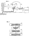
- FIG. 2 Apparatus for making the desired measurements and computations is schematically shown in FIG. 2.
- a reference workpiece 10 of known characteristics e.g. known etching profile
- a laser 30 is mounted and oriented for directing a beam of coherent light 31 onto the workpiece
- a photodiode 40 is movably mounted and oriented for receiving light 33 scattered from the workpiece.
- the output of photodiode 40 is an electrical signal representative of the scattered light intensity. This output is preferably applied via leads 41 to one terminal of a phase sensitive amplifier 50.
- the light from laser 30 is preferably passed through a chopper 32, and an electrical signal from the chopper indicative of the periods when laser light is passing through the chopper is applied via leads 34 to a second terminal of phase sensitive amplifier 50.
- the output of amplifier 50 is an electrical signal indicative of the intensity of the light received by photodiode 40 only when the laser beam is passing through the chopper. Thus the effects of ordinary ambient lighting can be ignored.
- This output is presented to a computer70 via leads 51.
- the photodiode 40 is preferably mounted on the rotating arm 61 of a rotational stage 60 with the axis of rotation aligned with the target area on the workpiece.
- This stage can be controlled by a computer 70 via leads 71 so that the computer controls the angular displacement of the photodiode.
- An exemplary arrangement of the apparatus of FIG. 2 employed a Melles Griot helium neon laser for laser 30, a Laser Precision chopper 32 and a Centronic OSDI-5B photodiode 40 with a 5mm, bugeye lens.
- the photodiode was mounted on a Newport Research Corp., Model 495 Optically Encoded Rotational Stage equipped with a Newport Model 855C Controller.
- Amplifier 50 was a Princeton Applied Research Model HR-8 phase sensitive amplifier.
- the computer 70 is programmed a) to measure and record the scattered light intensity over a wide range of angles, b) to calculate and record the spatial frequency F at each measurement, c) to determine an envelope function for the intensity versus frequency curve, and d) after the measurement of a plurality of samples, to determine one or more principal components of the intensity envelopes.
- the angle of incidence ⁇ i ; of beam 31, typically about 90°, and the wavelength ⁇ of laser 30, typically about 0.6328 micrometers, are entered into the computer.
- the location of photodiode 40 is conveniently initialized at spatial frequency zero by placing the diode in the specularly reflected beam.
- arm 61 is then rotated over an angular range between about 90° and 180° while several hundred intensity measurements are made and recorded.
- the range of spatial frequencies exceeds about one inverse micrometer encompassing more than 30 local maxima.
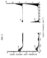
- FIGS. 4 and 5 show typical scattered light versus spatial frequency curves for a variety of workpieces. Specifically, the figures show the scattered light intensities for etched silicon test grids of 1.5 micrometer lines having spacing of 32 micrometers. Intensities were measured for both a normal incidence beam and for a grazing incidence beam.
- curve A the beam incidence was normal and the grid had lines with a vertical profile.
- Curve C is for the same grid but with a grazing incidence beam.
- Curve B is with beam incidence normal on a grid having lines which are "overcut”.
- Curve D is the same grid with the beam incidence at a grazing angle.
- curve A shows the intensity characteristic for a normal incidence on vertical profile grid of shallow etch depth.
- Curve C shows the result of a grazing incidence beam on the same grid.
- Curve B shows the characteristic for normal incidence on a grid of vertical profile with greater etching depth.
- Curve D shows the result of a grazing incidence beam on the same grid.
- the next step in the preferred preliminary process is to approximate the envelope of the intensity versus spatial frequency function thus measured.
- a preferred approach is as follows: First the function S1, of roughly 500 measured intensity versus frequency pairs, is transformed into an envelope function S2 by determining which of the points (I,F) correspond to local intensity maxima (I m ,F m ). An appropriate criterion is to choose as a local maximum each (I,F) pair wherein I is greater than or equal to the intensity values in the four pairs on either side of (I,F). This process leads to an envelope function of about 50 pairs, i.e. The specular maximum at and near the zero order is omitted from S2.
- the next step is to repeat the above-described process for a plurality of N measurements of regions having known characteristics. Applicants used 35 reference measurements from eight workpieces in their experiments.
- the result of this process is a plurality of interpolated envelope functions, where the nth envelope is (I n1 , I n2 , ..., In40), which can be represented as a N by 40 matrix.
- the next step in the preferred preliminary process is to determine one or more principal components of this matrix. This determination can be made by a computer in two steps. The first step is to subtract from each element in each column the mean value of elements in that respective column. This is referred to as centering the matrix, and the rows are now "centered" interpolated envelopes. The second step is to apply to the centered matrix, the singular value decomposition algorithm. For a detailed explanation of the singular value decomposition algorithm and its operation, see:
- the final step in the preferred preliminary process is to correlate the known properties of the reference measurements and the coordinates of the envelopes with respect to one or more principal components.
- Applicants determined that useful correlations concerning etching characteristics could be made by analyzing the centered, interpolated envelope function with respect to the first two principal components. In other words, if, for a given workpiece, the centered interpolated envelope function is approximated by the linear combination E ⁇ C1P1+C2P2, where C1 and C2 are constants referred to as coordinates, then C1 and C2 provide useful information concerning the etching characteristics of the workpiece.
- FIG. 6 plots for a run of 35 reference measurements with grids as described above.
- the area of the circles is proportional to known etch depth (with maximum depth of 2.8 micrometers)
- undercut etch profiles are denoted by a minus sign within the circle
- overcut etch profiles are denoted by a plus sign within the circle
- vertical etch profiles are denoted by empty circles.
- the correlation represented by the clustering of profiles with like characteristics permits well-defined criteria for inspection.
- the method for rapid and non-destructive testing of workpieces may be easily described in relation to FIG. 3.
- the workpiece to be inspected is exposed to a beam of light in the manner described in connection with FIG. 2, and, as shown in FIG. 3B, the scattered intensity, I, is then measured and recorded along with the calculated spatial frequency, F, as described above.
- the next step in the inspection process shown in FIG. 3C is to determine the coordinates of the centered interpolated intensity envelope with respect to one or more principal components, e.g., P1 and P2.
- the centered interpolated envelope function is generated in the same fashion as described above, and C1 and C2 are determined, such that C1P1+C2P2 provide the best least squares approximation to the envelope function. This determination is made in accordance with a linear regression algorithm or in accordance with other techniques well known in the art.
- the final step in the inspection process shown in FIG. 3D is to accept or reject the workpiece in accordance with whether or not the coordinates meet predetermined criteria. e.g. whether or not (C 1, C2) falls within a predetermined region, such as a rectangular region.
- predetermined criteria e.g. whether or not (C 1, C2) falls within a predetermined region, such as a rectangular region.
Abstract
Description
- The present invention relates to optical inspection of workpieces and, in particular, to a method for inspecting etched semiconductor workpieces using the principal components of scattered light intensity to distinguish differences in the nature of etched lines, including differences in profile, depth, slope and linewidth.
- It is common and necessary practice in the manufacture of integrated circuits to periodically inspect etched wafer workpieces for changes in critical line width, line profile and etched depths. Previously such inspections could be performed rapidly and non-destructively by a technician using an optical microscope. But as semiconductor technology has evolved to micron and sub-micron line widths, inspection by optical microscopy is no longer adequate. With today's submicron patterns, inspection typically involves selecting a sample of wafers from a processing lot, cleaving the wafers and inspecting the cleaved wafers with a scanning electron microscope. This approach is time-consuming, destructive and limited to a small subset of the wafer lot.
- In an effort to replace this time-consuming and destructive testing process, a variety of experimental efforts have been directed toward the development of inspection and monitoring methods based upon the scattering of a beam of light directed onto the workpiece surface. Such techniques have typically utilized only a narrow range of scattering angles, typically the specular intensity and the first order. While promising experimental results have been reported, these techniques have not demonstrated the ability to discriminate between submicron variations in etching depth and variations in etching profile.
- Applicants have discovered that if scattered light from an etched workpiece is measured over a range of spatial frequencies encompassing plural orders of diffraction, important characteristics of the etched workpiece can be correlated with the principal component content of the intensity characteristic.Thus an etched workpiece is inspected by 1) exposing the workpiece to a beam of coherent light, 2) measuring the intensity of the light scattered from the workpiece over a range of spatial frequencies corresponding to a plurality of diffraction orders, 3) computing the principal component coordinates of the intensity envelope, and 4) accepting or rejecting the workpiece in accordance with whether or not the principal component coordinates satisfy predetermined criteria. In a preferred embodiment the principal components are determined in relation to a plurality of reference measurements by computing the singular value decomposition.
-
- FIG. 1 is a block diagram illustrating a preferred method for determining a set of principal components for use in inspection;
- FIG. 2 is a schematic cross-section of typical apparatus for measuring scattered light intensity as a function of spatial frequency;
- FIG. 3 is a block diagram illustrating the steps involved in inspecting a workpiece in accordance with a preferred embodiment of the invention;
- FIGS. 4 and 5 are graphical illustrations, showing the scattered light intensity as a function of spatial frequency for various reference workpieces.
- FIG. 6 is a graphical illustration, plotting the coordinates with respect to the first and second principal components from intensity envelopes of 35 reference measurements.
- Applicants have discovered that if scattered light from a workpiece is measured over a range of spatial frequencies encompassing plural orders of diffraction, important characteristics of the workpiece can be correlated with the coordinates with respect to the principal components of the intensity envelope. This discovery permits rapid, non-destructive testing of workpieces, such as etched semiconductor workpieces, by measurement of their light scattering intensity envelopes and determination of the coordinates with respect to the principal components of those envelopes.
- The method of inspection may be best explained in two steps: first, a preliminary step of computing the principal components; and, second, using the coordinates with respect to principal components.
- As shown in FIG. 1, a preliminary step to inspection is 1) the computation of one or more principal components from reference workpieces of the type to be inspected and 2) correlation of the workpiece characteristics to be inspected with the values of the coordinates with respect to the principal components. While simple cases permit theoretical calculation of principal components, most practical applications require a preliminary step which involves measuring the light scattering characteristics of workpieces having known characteristics.
- As shown in FIG. 1A, the first step in the preliminary process is to select a workpiece of known characteristics, e.g., etching characteristics that are overcut, undercut, or straight profile, and to expose the workpiece to a beam of coherent light. The next step, shown in FIG. 1B, is to measure the intensity of the light scattered from the workpiece over plural orders of diffraction and to compute the spatial frequency F for each such intensity measurement.
- Apparatus for making the desired measurements and computations is schematically shown in FIG. 2. In essence, a
reference workpiece 10 of known characteristics (e.g. known etching profile) is disposed on asupport 20 which is preferably tiltable. Alaser 30 is mounted and oriented for directing a beam ofcoherent light 31 onto the workpiece, and aphotodiode 40 is movably mounted and oriented for receivinglight 33 scattered from the workpiece. The output ofphotodiode 40 is an electrical signal representative of the scattered light intensity. This output is preferably applied vialeads 41 to one terminal of a phasesensitive amplifier 50. The light fromlaser 30 is preferably passed through achopper 32, and an electrical signal from the chopper indicative of the periods when laser light is passing through the chopper is applied vialeads 34 to a second terminal of phasesensitive amplifier 50. With this arrangement, the output ofamplifier 50 is an electrical signal indicative of the intensity of the light received byphotodiode 40 only when the laser beam is passing through the chopper. Thus the effects of ordinary ambient lighting can be ignored. This output is presented to a computer70 vialeads 51. - The
photodiode 40 is preferably mounted on the rotatingarm 61 of arotational stage 60 with the axis of rotation aligned with the target area on the workpiece. This stage can be controlled by acomputer 70 via leads 71 so that the computer controls the angular displacement of the photodiode. - An exemplary arrangement of the apparatus of FIG. 2 employed a Melles Griot helium neon laser for
laser 30, a Laser Precisionchopper 32 and a Centronic OSDI-5B photodiode 40 with a 5mm, bugeye lens. The photodiode was mounted on a Newport Research Corp., Model 495 Optically Encoded Rotational Stage equipped with a Newport Model 855C Controller.Amplifier 50 was a Princeton Applied Research Model HR-8 phase sensitive amplifier. - The
computer 70 is programmed a) to measure and record the scattered light intensity over a wide range of angles, b) to calculate and record the spatial frequency F at each measurement, c) to determine an envelope function for the intensity versus frequency curve, and d) after the measurement of a plurality of samples, to determine one or more principal components of the intensity envelopes. - In practice, the angle of incidence Θi; of
beam 31, typically about 90°, and the wavelength λ oflaser 30, typically about 0.6328 micrometers, are entered into the computer. The location ofphotodiode 40 is conveniently initialized at spatial frequency zero by placing the diode in the specularly reflected beam. Under computer control,arm 61 is then rotated over an angular range between about 90° and 180° while several hundred intensity measurements are made and recorded. Preferably the range of spatial frequencies exceeds about one inverse micrometer encompassing more than 30 local maxima. Along with each intensity, I, the computer records the corresponding spatial frequency F calculated in accordance with the relation F=
- FIGS. 4 and 5 show typical scattered light versus spatial frequency curves for a variety of workpieces. Specifically, the figures show the scattered light intensities for etched silicon test grids of 1.5 micrometer lines having spacing of 32 micrometers. Intensities were measured for both a normal incidence beam and for a grazing incidence beam. In FIG. 4, curve A, the beam incidence was normal and the grid had lines with a vertical profile. Curve C is for the same grid but with a grazing incidence beam. Curve B is with beam incidence normal on a grid having lines which are "overcut". Curve D is the same grid with the beam incidence at a grazing angle.
- In FIG. 5, curve A shows the intensity characteristic for a normal incidence on vertical profile grid of shallow etch depth. Curve C shows the result of a grazing incidence beam on the same grid. Curve B shows the characteristic for normal incidence on a grid of vertical profile with greater etching depth. Curve D shows the result of a grazing incidence beam on the same grid.
- The next step in the preferred preliminary process, as shown as FIG. 1C, is to approximate the envelope of the intensity versus spatial frequency function thus measured. A preferred approach is as follows: First the function S₁, of roughly 500 measured intensity versus frequency pairs,

is transformed into an envelope function S₂ by determining which of the points (I,F) correspond to local intensity maxima (Im,Fm). An appropriate criterion is to choose as a local maximum each (I,F) pair wherein I is greater than or equal to the intensity values in the four pairs on either side of (I,F). This process leads to an envelope function of about 50 pairs, i.e.
The specular maximum at and near the zero order is omitted from S₂. - Since the frequencies in S₃ are not spaced the same from one reference workpiece to another, advantageously the next step shown in FIG. 1D is to generate an interpolated envelope function S₃ consisting of about 40 pairs having intensity values S₃ = (I1, I2, ..., I₄₀) linearly interpolated for a fixed set of frequencies (F₁, F₂, ..., F₄₀).
- As shown in FIG. 1E, the next step is to repeat the above-described process for a plurality of N measurements of regions having known characteristics. Applicants used 35 reference measurements from eight workpieces in their experiments. The result of this process is a plurality of interpolated envelope functions, where the nth envelope is (In1, In2, ..., In₄₀), which can be represented as a N by 40 matrix.
- The next step in the preferred preliminary process is to determine one or more principal components of this matrix. This determination can be made by a computer in two steps. The first step is to subtract from each element in each column the mean value of elements in that respective column. This is referred to as centering the matrix, and the rows are now "centered" interpolated envelopes. The second step is to apply to the centered matrix, the singular value decomposition algorithm. For a detailed explanation of the singular value decomposition algorithm and its operation, see:
- 1. T. F. Chan, "An Improved Algorithm for Compuring the Singular Value Decomposition," ACM Transactions on Mathematical Software,
Vol 8 No. 1, pp. 72-83 (1982). - 2. G. H. Golub and C. Reinsch, "Singular Value Decomposition and Least Squares Solutions," Numerische Mathematik 14, pp. 403-420 (1970).
- 3. L. Kaufman, "Application of Dense Householder Transformations to a Sparse Matrix," ACM Transactions on Mathematical Software, Vol. 5, No. 4, pp. 442-450 (1979). The result of the process is a new N by 40 matrix whose rows are the principal components (P₁, P₂, ..., Pn) which in various linear combinations can best approximate the centered interpolated envelopes of all reference measurements.
- The final step in the preferred preliminary process is to correlate the known properties of the reference measurements and the coordinates of the envelopes with respect to one or more principal components. Applicants determined that useful correlations concerning etching characteristics could be made by analyzing the centered, interpolated envelope function with respect to the first two principal components. In other words, if, for a given workpiece, the centered interpolated envelope function is approximated by the linear combination E≈C₁P₁+C₂P₂, where C₁ and C₂ are constants referred to as coordinates, then C₁ and C₂ provide useful information concerning the etching characteristics of the workpiece.
- An example of this correlation is shown in FIG. 6 which plots

for a run of 35 reference measurements with grids as described above. The area of the circles is proportional to known etch depth (with maximum depth of 2.8 micrometers), undercut etch profiles are denoted by a minus sign within the circle, overcut etch profiles are denoted by a plus sign within the circle, and vertical etch profiles are denoted by empty circles. As can be seen, the correlation represented by the clustering of profiles with like characteristics, permits well-defined criteria for inspection. The vertical profiles are bounded by C₁=[-0.2, -0.10] and C₂=[-0.1,0.0]. The overcut profiles are bounded by C₁=[0.15,0.30] and C₂=[-0.3,0.15]. Simpler or more complex regions could be used as inspection criteria. - With this preliminary process completed, the method for rapid and non-destructive testing of workpieces may be easily described in relation to FIG. 3. First, as shown in FIG. 3A, the workpiece to be inspected is exposed to a beam of light in the manner described in connection with FIG. 2, and, as shown in FIG. 3B, the scattered intensity, I, is then measured and recorded along with the calculated spatial frequency, F, as described above.
- The next step in the inspection process shown in FIG. 3C is to determine the coordinates of the centered interpolated intensity envelope with respect to one or more principal components, e.g., P₁ and P₂. The centered interpolated envelope function is generated in the same fashion as described above, and C₁ and C₂ are determined, such that C₁P₁+C₂P₂ provide the best least squares approximation to the envelope function. This determination is made in accordance with a linear regression algorithm or in accordance with other techniques well known in the art.
- The final step in the inspection process shown in FIG. 3D, is to accept or reject the workpiece in accordance with whether or not the coordinates meet predetermined criteria. e.g. whether or not (C1,C₂) falls within a predetermined region, such as a rectangular region. Thus workpieces of the type represented in FIG. 6 would pass if C₁=[-0.2,-0.10], C₂=[-0.1,0.0] corresponding to a vertical profile and fail if C₁=[0.15,0.30], C₂=[- 0.3,0.15] corresponding to an overcut profile.
Claims (6)
- A method for inspecting workpieces comprising the steps of:
exposing a workpiece to a beam of coherent light;
measuring the intensity of the light scattered from said workpiece over a range of spatial frequencies corresponding to a plurality of diffraction orders,
determining the principal component content of the intensity envelope for one or more principal components; and
accepting or rejecting said workpiece in accordance with whether or not said principle component content satisfies predetermined criteria. - The method according to claim 1 wherein the principal component content of the intensity envelope is determined by ascertaining the coefficients of said envelope with respect to one or more principal components.
- The method according to claim 2 wherein said principal component content of said intensity envelope is determined by ascertaining the coefficients of said envelope with respect to the first two principal components.
- The method according to claim 1 wherein said principal components are determined in relation to a plurality of reference measurements by singular value decomposition.
- The method of claims 1, 2, 3 or 4 wherein said workpiece is an etched semiconductor workpiece.
- The method of claims 1, 2, 3 or 4 wherein said workpiece is an etched semiconductor workpiece containing a test grid of etched lines and said step of exposing said wokkpiece comprises directing a beam of coherent light onto said test grid.
Applications Claiming Priority (2)
| Application Number | Priority Date | Filing Date | Title |
|---|---|---|---|
| US594774 | 1990-10-09 | ||
| US07/594,774 US5114233A (en) | 1990-10-09 | 1990-10-09 | Method for inspecting etched workpieces |
Publications (3)
| Publication Number | Publication Date |
|---|---|
| EP0480620A2 true EP0480620A2 (en) | 1992-04-15 |
| EP0480620A3 EP0480620A3 (en) | 1992-09-30 |
| EP0480620B1 EP0480620B1 (en) | 1994-12-28 |
Family
ID=24380353
Family Applications (1)
| Application Number | Title | Priority Date | Filing Date |
|---|---|---|---|
| EP91309019A Expired - Lifetime EP0480620B1 (en) | 1990-10-09 | 1991-10-02 | Method for inspecting etched workpieces |
Country Status (3)
| Country | Link |
|---|---|
| US (1) | US5114233A (en) |
| EP (1) | EP0480620B1 (en) |
| JP (1) | JPH0779119B2 (en) |
Cited By (5)
| Publication number | Priority date | Publication date | Assignee | Title |
|---|---|---|---|---|
| WO2003054475A2 (en) * | 2001-12-19 | 2003-07-03 | Kla-Tencor Technologies Corporation | Parametric profiling using optical spectroscopic systems |
| GB2411954A (en) * | 2004-03-12 | 2005-09-14 | Ingenia Technology Ltd | Determining a signature from an article to verify its authenticity |
| US7173699B2 (en) | 1998-03-06 | 2007-02-06 | Kla-Tencor Technologies Corporation | Spectroscopic scatterometer system |
| CN103293169A (en) * | 2012-02-27 | 2013-09-11 | 高雄应用科技大学 | Element image detection method and system thereof |
| US9818249B1 (en) | 2002-09-04 | 2017-11-14 | Copilot Ventures Fund Iii Llc | Authentication method and system |
Families Citing this family (28)
| Publication number | Priority date | Publication date | Assignee | Title |
|---|---|---|---|---|
| US5653894A (en) * | 1992-12-14 | 1997-08-05 | Lucent Technologies Inc. | Active neural network determination of endpoint in a plasma etch process |
| US5737496A (en) * | 1993-11-17 | 1998-04-07 | Lucent Technologies Inc. | Active neural network control of wafer attributes in a plasma etch process |
| US5739909A (en) * | 1995-10-10 | 1998-04-14 | Lucent Technologies Inc. | Measurement and control of linewidths in periodic structures using spectroscopic ellipsometry |
| US5658423A (en) * | 1995-11-27 | 1997-08-19 | International Business Machines Corporation | Monitoring and controlling plasma processes via optical emission using principal component analysis |
| DE19602445A1 (en) * | 1996-01-24 | 1997-07-31 | Nanopro Luftlager Produktions | Device and method for measuring two opposing surfaces of a body |
| US6728663B2 (en) | 2000-09-13 | 2004-04-27 | Accent Optical Technologies, Inc. | Structure identification using scattering signatures |
| JP3647378B2 (en) * | 2001-03-02 | 2005-05-11 | キヤノン株式会社 | Shape measuring apparatus and measuring method using multiprobe |
| EP1370828B1 (en) | 2001-03-02 | 2016-11-23 | Accent Optical Technologies, Inc. | Line profile asymmetry measurement using scatterometry |
| US7515279B2 (en) | 2001-03-02 | 2009-04-07 | Nanometrics Incorporated | Line profile asymmetry measurement |
| BRPI0508631A (en) | 2004-03-12 | 2007-08-07 | Ingenia Technology Ltd | apparatus for determining a signature of an article arranged in a reading volume, use of the apparatus, methods for identifying an article made of paper or cardboard, an article made of plastic, a product by its packaging, a document, a garment or footwear, and a disc, method for tagging an article, and, tagged article |
| WO2005088517A1 (en) | 2004-03-12 | 2005-09-22 | Ingenia Technology Limited | Methods and apparatuses for creating authenticatable printed articles and subsequently verifying them |
| GB2417592B (en) | 2004-08-13 | 2006-07-26 | Ingenia Technology Ltd | Authenticity verification of articles |
| WO2007012816A1 (en) | 2005-07-27 | 2007-02-01 | Ingenia Technology Limited | Verification of authenticity |
| EP1969525A1 (en) | 2005-12-23 | 2008-09-17 | Ingenia Holdings (UK)Limited | Optical authentication |
| US8145357B2 (en) * | 2007-12-20 | 2012-03-27 | Zodiac Pool Systems, Inc. | Residential environmental management control system with automatic adjustment |
| GB2466311B (en) | 2008-12-19 | 2010-11-03 | Ingenia Holdings | Self-calibration of a matching algorithm for determining authenticity |
| GB2476226B (en) | 2009-11-10 | 2012-03-28 | Ingenia Holdings Ltd | Optimisation |
| DE102011014866A1 (en) * | 2011-03-24 | 2012-09-27 | Carl Zeiss Jena Gmbh | Arrangement for monitoring and controlling of plasma etching process of workpiece, has image processing and simulation device that controls operation of ion beam source based on the measurement data of locator and detector array |
| US10386828B2 (en) * | 2015-12-17 | 2019-08-20 | Lam Research Corporation | Methods and apparatuses for etch profile matching by surface kinetic model optimization |
| US9792393B2 (en) * | 2016-02-08 | 2017-10-17 | Lam Research Corporation | Methods and apparatuses for etch profile optimization by reflectance spectra matching and surface kinetic model optimization |
| US10032681B2 (en) | 2016-03-02 | 2018-07-24 | Lam Research Corporation | Etch metric sensitivity for endpoint detection |
| US10197908B2 (en) | 2016-06-21 | 2019-02-05 | Lam Research Corporation | Photoresist design layout pattern proximity correction through fast edge placement error prediction via a physics-based etch profile modeling framework |
| US10254641B2 (en) | 2016-12-01 | 2019-04-09 | Lam Research Corporation | Layout pattern proximity correction through fast edge placement error prediction |
| US10534257B2 (en) | 2017-05-01 | 2020-01-14 | Lam Research Corporation | Layout pattern proximity correction through edge placement error prediction |
| US10572697B2 (en) | 2018-04-06 | 2020-02-25 | Lam Research Corporation | Method of etch model calibration using optical scatterometry |
| KR20200130870A (en) | 2018-04-10 | 2020-11-20 | 램 리써치 코포레이션 | Optical instrumentation in machine learning to characterize features |
| WO2019199697A1 (en) | 2018-04-10 | 2019-10-17 | Lam Research Corporation | Resist and etch modeling |
| US10977405B2 (en) | 2019-01-29 | 2021-04-13 | Lam Research Corporation | Fill process optimization using feature scale modeling |
Citations (4)
| Publication number | Priority date | Publication date | Assignee | Title |
|---|---|---|---|---|
| US4155098A (en) * | 1977-06-28 | 1979-05-15 | Rca Corporation | Groove depth estimation system using diffractive groove effects |
| GB2069691A (en) * | 1980-02-14 | 1981-08-26 | Rca Corp | Optical line width measuring apparatus and method |
| US4363118A (en) * | 1980-09-22 | 1982-12-07 | Rca Corporation | Sound carrier amplitude measurement system |
| US4408884A (en) * | 1981-06-29 | 1983-10-11 | Rca Corporation | Optical measurements of fine line parameters in integrated circuit processes |
Family Cites Families (4)
| Publication number | Priority date | Publication date | Assignee | Title |
|---|---|---|---|---|
| US4039370A (en) * | 1975-06-23 | 1977-08-02 | Rca Corporation | Optically monitoring the undercutting of a layer being etched |
| US4180830A (en) * | 1977-06-28 | 1979-12-25 | Rca Corporation | Depth estimation system using diffractive effects of the grooves and signal elements in the grooves |
| US4141780A (en) * | 1977-12-19 | 1979-02-27 | Rca Corporation | Optically monitoring the thickness of a depositing layer |
| US4303341A (en) * | 1977-12-19 | 1981-12-01 | Rca Corporation | Optically testing the lateral dimensions of a pattern |
-
1990
- 1990-10-09 US US07/594,774 patent/US5114233A/en not_active Expired - Lifetime
-
1991
- 1991-10-02 EP EP91309019A patent/EP0480620B1/en not_active Expired - Lifetime
- 1991-10-07 JP JP3285418A patent/JPH0779119B2/en not_active Expired - Fee Related
Patent Citations (4)
| Publication number | Priority date | Publication date | Assignee | Title |
|---|---|---|---|---|
| US4155098A (en) * | 1977-06-28 | 1979-05-15 | Rca Corporation | Groove depth estimation system using diffractive groove effects |
| GB2069691A (en) * | 1980-02-14 | 1981-08-26 | Rca Corp | Optical line width measuring apparatus and method |
| US4363118A (en) * | 1980-09-22 | 1982-12-07 | Rca Corporation | Sound carrier amplitude measurement system |
| US4408884A (en) * | 1981-06-29 | 1983-10-11 | Rca Corporation | Optical measurements of fine line parameters in integrated circuit processes |
Cited By (11)
| Publication number | Priority date | Publication date | Assignee | Title |
|---|---|---|---|---|
| US7173699B2 (en) | 1998-03-06 | 2007-02-06 | Kla-Tencor Technologies Corporation | Spectroscopic scatterometer system |
| US7859659B2 (en) | 1998-03-06 | 2010-12-28 | Kla-Tencor Corporation | Spectroscopic scatterometer system |
| US7898661B2 (en) | 1998-03-06 | 2011-03-01 | Kla-Tencor Corporation | Spectroscopic scatterometer system |
| WO2003054475A2 (en) * | 2001-12-19 | 2003-07-03 | Kla-Tencor Technologies Corporation | Parametric profiling using optical spectroscopic systems |
| WO2003054475A3 (en) * | 2001-12-19 | 2003-12-11 | Kla Tencor Corp | Parametric profiling using optical spectroscopic systems |
| US7280230B2 (en) | 2001-12-19 | 2007-10-09 | Kla-Tencor Technologies Corporation | Parametric profiling using optical spectroscopic systems |
| US7826071B2 (en) | 2001-12-19 | 2010-11-02 | Kla-Tencor Corporation | Parametric profiling using optical spectroscopic systems |
| US9818249B1 (en) | 2002-09-04 | 2017-11-14 | Copilot Ventures Fund Iii Llc | Authentication method and system |
| GB2411954A (en) * | 2004-03-12 | 2005-09-14 | Ingenia Technology Ltd | Determining a signature from an article to verify its authenticity |
| GB2411954B (en) * | 2004-03-12 | 2006-08-09 | Ingenia Technology Ltd | Authenticity verification methods,products and apparatuses |
| CN103293169A (en) * | 2012-02-27 | 2013-09-11 | 高雄应用科技大学 | Element image detection method and system thereof |
Also Published As
| Publication number | Publication date |
|---|---|
| EP0480620A3 (en) | 1992-09-30 |
| JPH04306857A (en) | 1992-10-29 |
| JPH0779119B2 (en) | 1995-08-23 |
| US5114233A (en) | 1992-05-19 |
| EP0480620B1 (en) | 1994-12-28 |
Similar Documents
| Publication | Publication Date | Title |
|---|---|---|
| EP0480620B1 (en) | Method for inspecting etched workpieces | |
| US4795260A (en) | Apparatus for locating and testing areas of interest on a workpiece | |
| US4957368A (en) | Apparatus and process for performing ellipsometric measurements of surfaces | |
| US5164790A (en) | Simple CD measurement of periodic structures on photomasks | |
| US4200396A (en) | Optically testing the lateral dimensions of a pattern | |
| US7003149B2 (en) | Method and device for optically monitoring fabrication processes of finely structured surfaces in a semiconductor production | |
| EP0464337A2 (en) | Measurement of size and refractive index of particles using the complex forward-scattered electromagnetic field | |
| US6806970B2 (en) | Thin film thickness measuring method and apparatus, and method and apparatus for manufacturing a thin film device using the same | |
| US6842259B2 (en) | Analysis of isolated and aperiodic structures with simultaneous multiple angle of incidence measurements | |
| US5867276A (en) | Method for broad wavelength scatterometry | |
| EP0163466B1 (en) | Method and apparatus for evaluating both thickness and compositional variables in a layered or thin film sample | |
| US20050057760A1 (en) | Critical dimension analysis with simultaneous multiple angle of incidence measurements | |
| GB2335982A (en) | Surface inspection device | |
| Zhenrong et al. | Roughness characterization of well-polished surfaces by measurements of light scattering distribution | |
| US6760100B2 (en) | Method and apparatus for classifying defects occurring at or near a surface of a smooth substrate | |
| US4168437A (en) | Optoelectric multi-sensor measuring apparatus and a method for measuring surface flatness therewith | |
| US7602509B1 (en) | Method for selecting optical configuration for high-precision scatterometric measurement | |
| Krukar et al. | Reactive ion etching profile and depth characterization using statistical and neural network analysis of light scattering data | |
| Giapis et al. | Use of light scattering in characterizing reactively ion etched profiles | |
| US4146330A (en) | Optical method and apparatus for surface roughness evaluation | |
| Tomassini et al. | Novel optical sensor for the measurement of surface texture | |
| Germer et al. | Proposed methodology for characterization of microroughness-induced optical scatter instrumentation | |
| Wang | The angle-limited integrated scattering (ALIS) measurement system for in-workshop inspection of the optical polishing process | |
| US5528648A (en) | Method and apparatus for analyzing contaminative element concentrations | |
| Stover et al. | Multiple particle technique for determination of differential scattering cross-section of very small surface bound particles |
Legal Events
| Date | Code | Title | Description |
|---|---|---|---|
| PUAI | Public reference made under article 153(3) epc to a published international application that has entered the european phase |
Free format text: ORIGINAL CODE: 0009012 |
|
| AK | Designated contracting states |
Kind code of ref document: A2 Designated state(s): FR GB |
|
| PUAL | Search report despatched |
Free format text: ORIGINAL CODE: 0009013 |
|
| AK | Designated contracting states |
Kind code of ref document: A3 Designated state(s): FR GB |
|
| 17P | Request for examination filed |
Effective date: 19930319 |
|
| RAP3 | Party data changed (applicant data changed or rights of an application transferred) |
Owner name: AT&T CORP. |
|
| 17Q | First examination report despatched |
Effective date: 19940519 |
|
| GRAA | (expected) grant |
Free format text: ORIGINAL CODE: 0009210 |
|
| AK | Designated contracting states |
Kind code of ref document: B1 Designated state(s): FR GB |
|
| ET | Fr: translation filed | ||
| PLBE | No opposition filed within time limit |
Free format text: ORIGINAL CODE: 0009261 |
|
| STAA | Information on the status of an ep patent application or granted ep patent |
Free format text: STATUS: NO OPPOSITION FILED WITHIN TIME LIMIT |
|
| 26N | No opposition filed | ||
| PGFP | Annual fee paid to national office [announced via postgrant information from national office to epo] |
Ref country code: GB Payment date: 20011008 Year of fee payment: 11 |
|
| REG | Reference to a national code |
Ref country code: GB Ref legal event code: IF02 |
|
| PG25 | Lapsed in a contracting state [announced via postgrant information from national office to epo] |
Ref country code: GB Free format text: LAPSE BECAUSE OF NON-PAYMENT OF DUE FEES Effective date: 20021002 |
|
| GBPC | Gb: european patent ceased through non-payment of renewal fee |
Effective date: 20021002 |
|
| PGFP | Annual fee paid to national office [announced via postgrant information from national office to epo] |
Ref country code: FR Payment date: 20101104 Year of fee payment: 20 |