EP0499346B1 - A method of testing an amplifier to establish its distortion characterstics due to intermodulation products - Google Patents
A method of testing an amplifier to establish its distortion characterstics due to intermodulation products Download PDFInfo
- Publication number
- EP0499346B1 EP0499346B1 EP92201343A EP92201343A EP0499346B1 EP 0499346 B1 EP0499346 B1 EP 0499346B1 EP 92201343 A EP92201343 A EP 92201343A EP 92201343 A EP92201343 A EP 92201343A EP 0499346 B1 EP0499346 B1 EP 0499346B1
- Authority
- EP
- European Patent Office
- Prior art keywords
- distortion
- amplifier
- amplitude
- phase
- tones
- Prior art date
- Legal status (The legal status is an assumption and is not a legal conclusion. Google has not performed a legal analysis and makes no representation as to the accuracy of the status listed.)
- Expired - Lifetime
Links
Images

Classifications
-
- H—ELECTRICITY
- H03—ELECTRONIC CIRCUITRY
- H03F—AMPLIFIERS
- H03F1/00—Details of amplifiers with only discharge tubes, only semiconductor devices or only unspecified devices as amplifying elements
- H03F1/32—Modifications of amplifiers to reduce non-linear distortion
- H03F1/3241—Modifications of amplifiers to reduce non-linear distortion using predistortion circuits
-
- G—PHYSICS
- G01—MEASURING; TESTING
- G01R—MEASURING ELECTRIC VARIABLES; MEASURING MAGNETIC VARIABLES
- G01R23/00—Arrangements for measuring frequencies; Arrangements for analysing frequency spectra
- G01R23/16—Spectrum analysis; Fourier analysis
- G01R23/20—Measurement of non-linear distortion
Definitions
- the present invention relates to a method of testing an amplifier to establish its distortion characteristics due to intermodulation products.
- IMPs intermodulation products
- the IMPs therefore distort the output and hence cause interference in adjacent channels.
- This effect gives rise to a significant technical problem where the frequency of the input signal to the final power amplifier stage represents information, for example if the input signal is the output of a parallel tone modem, or where the transmitter is being used to transmit several different signals at the same carrier frequency, as in an independent sideband mode of operation.
- a typical specification requires that any IMPs should be reduced by at least -35dB relative to the wanted signals.
- EP-A-0097,845 discloses a device for determining the attenuation distortion and the group delay distortion of a device under test, particularly a data transmission device.
- the present invention is concerned with the problem of correcting for the effect of IMPs when an amplifier may be able to operate at any frequency within a wide frequency range. In order that this may be possible, it is necessary to be able to accurately measure the distortion over the whole frequency range of the amplifier. A novel technique for carrying out this measurement is described herein.
- a method of testing an amplifier in order to establish its distortion characteristics due to intermodulation products comprising the steps of generating two signal tones to be fed simultaneously to the amplifier under test, mixing the output of the amplifier with a local oscillator frequency, sampling the voltage at the output of the mixer periodically, and carrying out a Fourier transform on the samples, in order to derive amplitude and phase information for a plurality of sample frequencies within the amplifier output, identifying distorting IMPS and determining the phase and amplitude distortion produced thereby relative to the amplitude of the vector sum of the two tones, and repeating the preceding steps for pairs of tones throughout the frequency range of the amplifier.
- pre-distortion circuits suitable for offsetting these effects can then be selected for incorporation into the transmitter so that, whatever the radio frequency of the signal to be transmitted, the input to the amplifier can be routed through an appropriate pre-distortion circuit in order to minimise the intermodulation products.
- a bank of three pre-distortion circuits can cover the whole HF range (e.g. 1.6 to 30 MHz) and ensure that all order IMPs are reduced to at least -40dB.
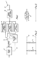
- An HF radio transmitter as illustrated in Figure 1 comprises essentially conventional mixing stages 2 for converting an input signal, such as a voice signal or the output of a parallel tone modem, into an RF signal at an output 4.
- the output RF signal is passed to one of a bank of three pre-distortion circuits 8, 10, 12 via a selection switch 14, the position of which is controlled by a selection control unit 16.
- the outputs of all three pre-distortion circuits are connected to an input of a power amplifier 20.
- the output of the power amplifier is connected to an antenna 22 for transmission.
- the selection control unit is shown as connected via a control line 18 to the mixing stages 2 in order to indicate that the setting of the selection switch 14 is determined by the RF frequency of the output signal as determined by the user.
- the desired RF frequency of the output is, of course, used to determine the local oscillator frequencies employed during the mixing stages 2.
- the input means employed by the user to set the RF frequency and, therefore the local oscillator frequencies in the mixing stages may also be connected to control the selection switch.
- Each pre-distortion circuit is capable of producing a required mixture of amplitude and phase distortion, as determined by the previously measured distortion produced within each frequency range by the power amplifier 20, for a particular portion of the frequency range of the amplifier 20.
- the output of the power amplifier is an amplified, but otherwise substantially identical, version of the RF signal presented at the output 4 of the mixing stages 2.
- the pre-distortion circuits 8, 10, and 12 In order to determine the appropriate design of the pre-distortion circuits 8, 10, and 12 and the number of such pre-distortion circuits required, it is necessary to measure the types of distortion produced by the amplifier 20 accurately throughout its operating frequency range. This may be done by employing the apparatus illustrated in Figure 4, which will now be described.
- Figures 2 and 3 show suitable designs for the pre-distortion circuits 8, 10 or 12. The value and type (resistor, inductor, capacitor or combination thereof) of the impedances Z employed is determined by the distortion to be corrected as will be described in more detail later.
- the amplifier 20 is typically a class B linear amplifier designed using solid state components.
- the input signal is chosen as two RF tones at slightly different frequencies separated by, for example, 2kHz so as to generate intermodulation products, which are the particular concern of the present invention.
- the amplifier may also be subject to other types of distortion, such as distortion due to harmonics.
- the pre-distortion circuits may be able to compensate for such alternative types of distortion to some extent at the same time as dealing with the IMPs.
- a two tone input to the amplifier 20 is provided by two signal generators 22, 24 operating at two distinct frequencies separated by, say, 2kHz in the HF range.
- the output of the amplifier is fed via a mixer 26 to a sampling voltmeter 28.
- the mixer 26 is provided with its second input from a signal generator 30 set to a suitable frequency to produce an output in which the two input tones generated by the signal generators 22 and 24 are mixed down to 20kHz and 22kHz respectively.
- the frequency standards of the generators 22, 24 and 30 are connected together as shown by the dotted control line 32.
- the sampling voltmeter produces digital samples of the mixed down output of the amplifier 20.
- the samples are fed to a computer 34 which is programmed to perform a Fourier transform on the output signal using a FFT algorithm, and also to further process the results of the FFT in order to produce plots of the spectrum of the output signal, the amplitude distortion and the phase distortion on displays or as print-outs as shown by blocks 36,38,40. It will be appreciated that these functions can readily be carried out by suitable programmes which need not be described in detail herein except for the functions which they perform which are set out more fully below.
- sampling voltmeter 28 may be limited in its sampling rate, it may be necessary to sample at time intervals so that each successive sample of the waveform is actually taken from a following cycle of the signal rather than the same cycle. This produces the same results since the individual cycles, though subject to distortion, will be identical.
- the FFT is to use 512 (2N) samples over a period (T) of 2 ms, samples should be taken every 0.0039 ms. However, provided all the significant frequency components are multiples of 1kHz samples may be taken at every 1.0039 ms instead. This will enable the signal output from the mixer 26 to be analysed over a frequency range of 128kHz.
- the output of the FFT contains amplitude and phase information for each of 256 (N) sample frequencies within the analysis range from 0.5kHz to 128kHz in steps of 0.5kHz (1/T).
- the first output from the processor 34 on display 36 which may be a CRT or plotter or both, is the spectrum of the output signal, that is the amplitude of each sample frequency versus frequency.
- the amplifier 20 If there is no distortion produced by the amplifier 20, this will show only the two tones at 20 and 22 kHz respectively. However, the spectrum will normally also include IMPs at various levels and harmonics. The third order IMPs will be at 18 and 24 kHz, the fifth order at 16 and 26 kHz and so on.
- the programme run by the computer 34 first identifies in the spectrum the two tones and computes the vector sum of these two tones as shown in Figure 5, where the first tone is identified by the vector 44 which can be expressed as A1e -j( ⁇ 1 t+ ⁇ 1 ) .
- the second tone is shown by the vector 46 as A2e -j( ⁇ 2 t+ ⁇ 2 ) .
- ⁇ 1 - ⁇ 2 will be a constant value.
- the maximum amplitudes of the signals, A1 and A2 are ideally equal.
- the vector sum of the two tones 44 and 46 is shown by the vector 48. It will be appreciated that the vector 48 rotates in time and that its amplitude will change as a function of time since the frequencies of its two components are different.
- the phase of the vector sum 48 of the two tones is used as a reference phase throughout the following analysis.
- the average frequency of the two tones that is 21kHz in the present example, is also used as a reference frequency. Therefore, relative to this reference, the two tones have frequencies of plus and minus 1kHz respectively, resulting in their vector sum 48 having a constant phase.
- the computer programme identifies from the output of the FFT those sample frequencies at which there is a large signal, that is one having an amplitude greater than a predetermined threshold value.
- the threshold may be determined by reference to the amplitude of the signals at the sample frequencies corresponding to the input tones and the required level to which all IMPs are to be reduced as determined by the design specification for the amplifier. Only signals which are at IMP frequencies (e.g. ⁇ 3kHz, ⁇ 5kHz etc.) are used in the following calculations. The other large signals are monitored just as a check on the test. There should be no large signals except the IMPs and the harmonics. The phase of these IMPs relative to the reference phase is then computed.
- the vector sum of the IMPs for a number of points, typically 200 during a 1 millisecond period, which corresponds to 1kHz and therefore covers a complete cycle of the vector sum of the two tones.
- the component of the vector sum of the IMPs which is in phase with the vector sum of the two tones is then computed. This component represents the amplitude distortion and is plotted against the two tone amplitude for the purposes of the display or printout 38.
- the component of the vector sum of the IMPs at 90° to the reference phase represents the phase distortion. This is plotted against the two tone amplitude for output 40.
- Plots of the spectrum as shown on display 36, the amplitude distortion plot as shown on display 38 and the phase distortion plot as shown on display 40 are obtained and preferably printed for two tones generated by the signal generators 22 and 24 at various points in the frequency range of the amplifier 20.
- a plot of the waveform in time may also be generated if required to measure the frequency.
- a simple and effective way of producing distortion is to use pairs of diodes and impedances.
- a circuit as shown in Figure 2 will compensate for the cross over type of amplitude distortion illustrated in Figure 6b, if the impedances Z are suitable resistances.
- the diodes 54 and 56 which are preferably Schottky diodes, are non-conducting
- the output voltage across terminals 58 is not affected by the predistortion circuit, whereas at higher voltages or amplitudes at which the diodes conduct, the resistance produces a greater attenuation to offset the increased grain of the amplifier.
- the value of the resistance is determined by the amount by which the gain increases with amplitude.
- the circuit shown in Figure 3 corrects for the type of distortion illustrated in Figure 6a when the impedance Z is a resistance. In this case the circuit has no effect when the diodes 60, 62 are conducting but has the effect of decreasing the gain at low amplitudes when the diodes are off.
- Corrections can be made to the phase distortion by the use of similar circuits in which Z is an inductance or a capacitance.
- Z is an inductance or a capacitance.
- the shunt circuit of Figure 2 gives a phase change when the diodes turn on and the series circuit of Figure 3 gives a phase change when the diodes turn off.
- the necessary correction can be achieved by the use of inductors in either the circuit of Figure 2 or Figure 3. Normally since amplitude distortion will need to be corrected at the same time, this determines the choice of the type of circuit between Figures 2 and 3 and a resistive inductor will be used as the impedance Z.
- the use of a capacitive impedance will compensate for the type of phase distortion illustrated in Figure 6d.
- Pre-distortion circuits may also be designed using the circuits shown in Figures 2 and 3 in series with the values of Z selected in accordance with the type of distortion measured using the apparatus shown in Figure 4.
- results derived from the use of the apparatus shown in Figure 4 may also be used to assist the design of the amplifier 20 by appropriate choice of bias current and selection of components.
Landscapes
- Physics & Mathematics (AREA)
- Nonlinear Science (AREA)
- Engineering & Computer Science (AREA)
- Power Engineering (AREA)
- Mathematical Physics (AREA)
- General Physics & Mathematics (AREA)
- Amplifiers (AREA)
Description
- The present invention relates to a method of testing an amplifier to establish its distortion characteristics due to intermodulation products.
- When a transmitter is required to transmit a signal which contains components at several distinct frequencies, non-linearities in the final power amplifier give rise to intermodulation products (IMPs) at the output of the amplifier at frequencies other than those present in the input signal. The IMPs therefore distort the output and hence cause interference in adjacent channels. This effect gives rise to a significant technical problem where the frequency of the input signal to the final power amplifier stage represents information, for example if the input signal is the output of a parallel tone modem, or where the transmitter is being used to transmit several different signals at the same carrier frequency, as in an independent sideband mode of operation. For such purposes, a typical specification requires that any IMPs should be reduced by at least -35dB relative to the wanted signals. Although it is possible to achieve this with amplifiers using valves, it has hitherto been difficult and impractical to produce IMPs reduced by more than -30dB with solid state class B linear amplifiers operating at radio frequencies.
- Typically, attempts have been made to reduce distortion in such amplifiers by the use of inverted feedback techniques and a number of amplifier stages, in order to compensate for the reduction in gain produced by the negative feedback. Improvements may also be obtained by carefully selecting the biasing conditions of the transistors used. Such design considerations are well discussed in the literature. However, such techniques have been found ineffective in meeting the high specifications required.
- Comsat Technical Review, Vol 15, No.2 (1985), Part A, pages 272-308, discloses a different approach whereby a linear power amplifier is provided with a plurality of individually selectable pre-distortion circuits.
- EP-A-0097,845 discloses a device for determining the attenuation distortion and the group delay distortion of a device under test, particularly a data transmission device.
- The present invention is concerned with the problem of correcting for the effect of IMPs when an amplifier may be able to operate at any frequency within a wide frequency range. In order that this may be possible, it is necessary to be able to accurately measure the distortion over the whole frequency range of the amplifier. A novel technique for carrying out this measurement is described herein.
- In accordance with the invention, there is provided a method of testing an amplifier in order to establish its distortion characteristics due to intermodulation products, comprising the steps of generating two signal tones to be fed simultaneously to the amplifier under test, mixing the output of the amplifier with a local oscillator frequency, sampling the voltage at the output of the mixer periodically, and carrying out a Fourier transform on the samples, in order to derive amplitude and phase information for a plurality of sample frequencies within the amplifier output, identifying distorting IMPS and determining the phase and amplitude distortion produced thereby relative to the amplitude of the vector sum of the two tones, and repeating the preceding steps for pairs of tones throughout the frequency range of the amplifier.
- Using such a test, it is possible to identify the intermodulation products due to non-linear gain, and plot changes in phase and amplitude with signal amplitude which result in the distortion of the input signal throughout the frequency range. The appropriate types of pre-distortion circuits suitable for offsetting these effects can then be selected for incorporation into the transmitter so that, whatever the radio frequency of the signal to be transmitted, the input to the amplifier can be routed through an appropriate pre-distortion circuit in order to minimise the intermodulation products. Typically, it has been found that a bank of three pre-distortion circuits can cover the whole HF range (e.g. 1.6 to 30 MHz) and ensure that all order IMPs are reduced to at least -40dB. However it is preferred to repeat the test for more than three frequencies from the range of the amplifier.
- A method of measuring the distortion of the power amplifier in accordance with the invention will now be described, by way of example only, with reference to the accompanying diagrammatic drawings, in which:
- Figure 1 is a block diagram of an HF transmitter;
- Figure 2 is a pre-distortion circuit for compensating a first type of distortion;
- Figure 3 is a pre-distortion circuit for compensating a second type of distortion;
- Figure 4 is a test set-up for use in designing the transmitter of Figure 1;
- Figure 5 is a vector diagram for illustrating the input signal to an amplifier to be tested with the apparatus of Figure 4; and
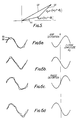
- Figures 6a to 6d show, on the left hand side amplitude versus time plots of various distorted output signals from an amplifier fed with two tones as in the apparatus of Figure 4, and, on the right hand side, corresponding plots of the amplitude or phase distortion relative to the two tone amplitude.
- An HF radio transmitter as illustrated in Figure 1 comprises essentially
conventional mixing stages 2 for converting an input signal, such as a voice signal or the output of a parallel tone modem, into an RF signal at an output 4. The output RF signal is passed to one of a bank of three pre-distortioncircuits selection switch 14, the position of which is controlled by aselection control unit 16. The outputs of all three pre-distortion circuits are connected to an input of apower amplifier 20. The output of the power amplifier is connected to anantenna 22 for transmission. - The selection control unit is shown as connected via a
control line 18 to themixing stages 2 in order to indicate that the setting of theselection switch 14 is determined by the RF frequency of the output signal as determined by the user. The desired RF frequency of the output is, of course, used to determine the local oscillator frequencies employed during themixing stages 2. The input means employed by the user to set the RF frequency and, therefore the local oscillator frequencies in the mixing stages may also be connected to control the selection switch. Each pre-distortion circuit is capable of producing a required mixture of amplitude and phase distortion, as determined by the previously measured distortion produced within each frequency range by thepower amplifier 20, for a particular portion of the frequency range of theamplifier 20. - Because of the presence of the pre-distortion circuits, the output of the power amplifier is an amplified, but otherwise substantially identical, version of the RF signal presented at the output 4 of the
mixing stages 2. In order to determine the appropriate design of thepre-distortion circuits amplifier 20 accurately throughout its operating frequency range. This may be done by employing the apparatus illustrated in Figure 4, which will now be described. Figures 2 and 3 show suitable designs for thepre-distortion circuits - The
amplifier 20 is typically a class B linear amplifier designed using solid state components. For testing purposes, the input signal is chosen as two RF tones at slightly different frequencies separated by, for example, 2kHz so as to generate intermodulation products, which are the particular concern of the present invention. It will be appreciated that the amplifier may also be subject to other types of distortion, such as distortion due to harmonics. The pre-distortion circuits may be able to compensate for such alternative types of distortion to some extent at the same time as dealing with the IMPs. - A two tone input to the
amplifier 20 is provided by twosignal generators mixer 26 to asampling voltmeter 28. Themixer 26 is provided with its second input from asignal generator 30 set to a suitable frequency to produce an output in which the two input tones generated by thesignal generators - The frequency standards of the
generators dotted control line 32. - The sampling voltmeter produces digital samples of the mixed down output of the
amplifier 20. The samples are fed to acomputer 34 which is programmed to perform a Fourier transform on the output signal using a FFT algorithm, and also to further process the results of the FFT in order to produce plots of the spectrum of the output signal, the amplitude distortion and the phase distortion on displays or as print-outs as shown byblocks - Since the
sampling voltmeter 28 may be limited in its sampling rate, it may be necessary to sample at time intervals so that each successive sample of the waveform is actually taken from a following cycle of the signal rather than the same cycle. This produces the same results since the individual cycles, though subject to distortion, will be identical. Thus, if the FFT is to use 512 (2N) samples over a period (T) of 2 ms, samples should be taken every 0.0039 ms. However, provided all the significant frequency components are multiples of 1kHz samples may be taken at every 1.0039 ms instead. This will enable the signal output from themixer 26 to be analysed over a frequency range of 128kHz. This is actually a larger range than may be considered strictly necessary but arises because of the requirement of the FFT algorithm to have a number of samples which is a power of 2. For the purposes of the present invention analysis of distortion due to IMPs up to the 7th order is generally all that is necessary, since higher order IMPs produce distortions which are already of a sufficiently low level and do not require further compensation. The output of the FFT contains amplitude and phase information for each of 256 (N) sample frequencies within the analysis range from 0.5kHz to 128kHz in steps of 0.5kHz (1/T). The first output from theprocessor 34 ondisplay 36, which may be a CRT or plotter or both, is the spectrum of the output signal, that is the amplitude of each sample frequency versus frequency. If there is no distortion produced by theamplifier 20, this will show only the two tones at 20 and 22 kHz respectively. However, the spectrum will normally also include IMPs at various levels and harmonics. The third order IMPs will be at 18 and 24 kHz, the fifth order at 16 and 26 kHz and so on. - In order to analyse the phase and amplitude information generated by the FFT, it is required to plot the phase and amplitude distortion versus the two tone signal amplitude. Typical such plots are shown in Figures 6a - 6d for various types of distortion. In order to produce these plots, the programme run by the
computer 34 first identifies in the spectrum the two tones and computes the vector sum of these two tones as shown in Figure 5, where the first tone is identified by thevector 44 which can be expressed as
vector 46 as
signal generators tones vector 48. It will be appreciated that thevector 48 rotates in time and that its amplitude will change as a function of time since the frequencies of its two components are different. The phase of thevector sum 48 of the two tones is used as a reference phase throughout the following analysis. - The average frequency of the two tones, that is 21kHz in the present example, is also used as a reference frequency. Therefore, relative to this reference, the two tones have frequencies of plus and minus 1kHz respectively, resulting in their
vector sum 48 having a constant phase. - The computer programme identifies from the output of the FFT those sample frequencies at which there is a large signal, that is one having an amplitude greater than a predetermined threshold value. The threshold may be determined by reference to the amplitude of the signals at the sample frequencies corresponding to the input tones and the required level to which all IMPs are to be reduced as determined by the design specification for the amplifier. Only signals which are at IMP frequencies (e.g. ±3kHz, ±5kHz etc.) are used in the following calculations. The other large signals are monitored just as a check on the test. There should be no large signals except the IMPs and the harmonics. The phase of these IMPs relative to the reference phase is then computed. From this information it is possible to calculate the vector sum of the IMPs for a number of points, typically 200 during a 1 millisecond period, which corresponds to 1kHz and therefore covers a complete cycle of the vector sum of the two tones. The component of the vector sum of the IMPs which is in phase with the vector sum of the two tones is then computed. This component represents the amplitude distortion and is plotted against the two tone amplitude for the purposes of the display or
printout 38. The component of the vector sum of the IMPs at 90° to the reference phase represents the phase distortion. This is plotted against the two tone amplitude foroutput 40. - There are four basic shapes for these plots. However, any particular amplifier under test may produce modifications of these shapes. The two basic shapes of the amplitude distortion plots are shown on the right hand side in Figures 6a and 6b with the effect they have on the actual waveform shown on the left hand side where voltage is plotted against time, the
solid line waveforms 50 showing the ideal, undistorted waveform, and the dotted line 52 showing the distorted waveform. - As shown in Figure 6a, there is positive amplitude distortion at low levels of the two tone amplitude and negative amplitude distortion at high levels. This is caused by the gain of the
amplifier 20 decreasing with amplitude as can be seen by a comparison of thewaveforms 50 and 52 on the left hand side of Figure 6a. - The amplitude distortion plot shown in Figure 6b shows the result of gain decreasing with amplitude. This type of distortion is known as cross over distortion.
- Similar plots for phase distortion are shown in Figures 6c and 6d. In Figure 6c the distortion is due to the delay through the amplifier increasing with the amplitude of the signal. The reverse situation is illustrated in Figure 6d.
- Plots of the spectrum as shown on
display 36, the amplitude distortion plot as shown ondisplay 38 and the phase distortion plot as shown ondisplay 40 are obtained and preferably printed for two tones generated by thesignal generators amplifier 20. A plot of the waveform in time may also be generated if required to measure the frequency. These results can then be analysed to determine how best to design the predistortion circuits in order to compensate for the types of distortion found at various frequencies within the operating range of the amplifier. Typically it will be necessary to separate this operating range into a number of sub-ranges which have different distortion characteristics. For each range a suitable predistortion circuit is designed which gives the opposite change in gain and phase with amplitude to that produced by theamplifier 20. - A simple and effective way of producing distortion is to use pairs of diodes and impedances. A circuit as shown in Figure 2 will compensate for the cross over type of amplitude distortion illustrated in Figure 6b, if the impedances Z are suitable resistances. At low amplitudes, where the
diodes terminals 58 is not affected by the predistortion circuit, whereas at higher voltages or amplitudes at which the diodes conduct, the resistance produces a greater attenuation to offset the increased grain of the amplifier. The value of the resistance is determined by the amount by which the gain increases with amplitude. - The circuit shown in Figure 3 corrects for the type of distortion illustrated in Figure 6a when the impedance Z is a resistance. In this case the circuit has no effect when the
diodes 60, 62 are conducting but has the effect of decreasing the gain at low amplitudes when the diodes are off. - Corrections can be made to the phase distortion by the use of similar circuits in which Z is an inductance or a capacitance. Thus the shunt circuit of Figure 2 gives a phase change when the diodes turn on and the series circuit of Figure 3 gives a phase change when the diodes turn off. For the type of phase distortion illustrated in Figure 6c, the necessary correction can be achieved by the use of inductors in either the circuit of Figure 2 or Figure 3. Normally since amplitude distortion will need to be corrected at the same time, this determines the choice of the type of circuit between Figures 2 and 3 and a resistive inductor will be used as the impedance Z. The use of a capacitive impedance will compensate for the type of phase distortion illustrated in Figure 6d.
- Pre-distortion circuits may also be designed using the circuits shown in Figures 2 and 3 in series with the values of Z selected in accordance with the type of distortion measured using the apparatus shown in Figure 4.
- The results derived from the use of the apparatus shown in Figure 4 may also be used to assist the design of the
amplifier 20 by appropriate choice of bias current and selection of components.
Claims (2)
- A method of testing an amplifier (20) in order to establish its distortion characteristics due to intermodulation products, comprising the step of generating two signal tones to be fed simultaneously to the amplifier (20) under test, characterised by the further steps of mixing the output of the amplifier with a local oscillator frequency, sampling the voltage at the output of the mixer (26) periodically, and carrying out a Fourier transform on the samples in order to derive amplitude and phase information for a plurality of sample frequencies within the amplifier output, identifying distorting intermodulation products and determining the phase and amplitude distortion produced thereby relative to the amplitude of the vector sum of the two tones, and repeating the preceding steps for pairs of tones throughout the frequency range of the amplifier (20).
- A method as claimed in claim 1, characterised by the step of determining the phase and amplitude distortion comprises the steps of determining the vector sum of the distorting intermodulation products and plotting its components in phase with and at 90° to the vector sum of the two tones, against the amplitude of the two tones over a time period during which the two tone amplitude completes a cycle, in order to derive plots of the amplitude and phase distortion respectively.
Applications Claiming Priority (3)
| Application Number | Priority Date | Filing Date | Title |
|---|---|---|---|
| GB8709998A GB2204202B (en) | 1987-04-28 | 1987-04-28 | Radio transmitters |
| GB8709998 | 1987-04-28 | ||
| EP88302588A EP0289130B1 (en) | 1987-04-28 | 1988-03-24 | Radio transmitters |
Related Parent Applications (1)
| Application Number | Title | Priority Date | Filing Date |
|---|---|---|---|
| EP88302588.4 Division | 1988-03-24 |
Publications (2)
| Publication Number | Publication Date |
|---|---|
| EP0499346A1 EP0499346A1 (en) | 1992-08-19 |
| EP0499346B1 true EP0499346B1 (en) | 1995-12-06 |
Family
ID=10616461
Family Applications (2)
| Application Number | Title | Priority Date | Filing Date |
|---|---|---|---|
| EP92201343A Expired - Lifetime EP0499346B1 (en) | 1987-04-28 | 1988-03-24 | A method of testing an amplifier to establish its distortion characterstics due to intermodulation products |
| EP88302588A Expired - Lifetime EP0289130B1 (en) | 1987-04-28 | 1988-03-24 | Radio transmitters |
Family Applications After (1)
| Application Number | Title | Priority Date | Filing Date |
|---|---|---|---|
| EP88302588A Expired - Lifetime EP0289130B1 (en) | 1987-04-28 | 1988-03-24 | Radio transmitters |
Country Status (4)
| Country | Link |
|---|---|
| US (1) | US4890300A (en) |
| EP (2) | EP0499346B1 (en) |
| DE (2) | DE3879259T2 (en) |
| GB (2) | GB2204202B (en) |
Families Citing this family (64)
| Publication number | Priority date | Publication date | Assignee | Title |
|---|---|---|---|---|
| US4857865A (en) * | 1988-11-10 | 1989-08-15 | Hughes Aircraft Company | Self equalizing multi-stage radio frequency power amplifier |
| FR2642243B1 (en) * | 1989-01-24 | 1991-04-19 | Labo Electronique Physique | ADAPTIVE PREDISTORSION CIRCUIT |
| JP2824123B2 (en) * | 1989-05-30 | 1998-11-11 | キヤノン株式会社 | Ink jet head and substrate for ink jet head used to form the head |
| JPH03145346A (en) * | 1989-10-31 | 1991-06-20 | Nec Corp | Car telephone system |
| IT1236905B (en) * | 1989-12-21 | 1993-04-26 | SYSTEM FOR SETTING UP TRANSMITTERS IN LARGE CAPACITY DIGITAL RADIO LINKS | |
| US5251328A (en) * | 1990-12-20 | 1993-10-05 | At&T Bell Laboratories | Predistortion technique for communications systems |
| GB9111926D0 (en) * | 1991-06-04 | 1991-07-24 | Nat Transcommunications Ltd | An improved method of video noise reduction using non-linear pre/de-emphasis |
| SE468616B (en) * | 1991-06-12 | 1993-02-15 | Ericsson Telefon Ab L M | PROCEDURE FOR COMPENSATION OF THE TRANSMITTER USE SIGNAL'S DEPENDENCE OF THE TRANSFER FUNCTION FOR A COMBINER FILTER |
| US5412691A (en) * | 1991-06-28 | 1995-05-02 | Digital Equipment Corporation | Method and apparatus for equalization for transmission over a band-limited channel |
| GB2257860B (en) * | 1991-07-06 | 1995-09-20 | Racal Communications Syst Ltd | Amplification systems |
| DE4134472C2 (en) * | 1991-10-18 | 1994-01-27 | Rohde & Schwarz | Method for measuring the distortion factor of an AC voltage signal |
| US5266951A (en) * | 1991-12-30 | 1993-11-30 | Raytheon Company | Analog to digital converter calibration system and method of operation |
| GB2265269B (en) * | 1992-03-02 | 1995-08-30 | Motorola Ltd | Radio transmitter with linearization training sequence |
| DE69222634T2 (en) * | 1992-07-10 | 1998-02-05 | Thomcast | System and method for correcting the sound carrier |
| FR2707127A1 (en) * | 1993-06-29 | 1995-01-06 | Philips Laboratoire Electroniq | Digital transmission system with predisposition. |
| US6288814B1 (en) * | 1994-05-19 | 2001-09-11 | Ortel Corporation | In-line predistorter for linearization of electronic and optical signals |
| US5523716A (en) * | 1994-10-13 | 1996-06-04 | Hughes Aircraft Company | Microwave predistortion linearizer |
| US5748678A (en) * | 1995-07-13 | 1998-05-05 | Motorola, Inc. | Radio communications apparatus |
| JPH09199948A (en) * | 1996-01-12 | 1997-07-31 | Fujitsu Ltd | Nonlinear compensation circuit |
| US5732333A (en) * | 1996-02-14 | 1998-03-24 | Glenayre Electronics, Inc. | Linear transmitter using predistortion |
| US6173161B1 (en) * | 1996-09-25 | 2001-01-09 | Lucent Technologies Inc. | Signal improvement by predistortion/postdistortion programmable converter |
| CA2274718A1 (en) * | 1996-12-24 | 1998-07-02 | Gte Government Systems Corporation | Symbol lock detector |
| US5987069A (en) * | 1996-12-24 | 1999-11-16 | Gte Government Systems Corporation | Method and apparatus for variably allocating upstream and downstream communication spectra |
| US6549242B1 (en) * | 1997-04-04 | 2003-04-15 | Harris Corporation | Combining adjacent TV channels for transmission by a common antenna |
| US5798674A (en) * | 1997-04-08 | 1998-08-25 | Raytheon Company | Band Limited AM modulator using linear power amplification |
| KR100251561B1 (en) | 1997-06-19 | 2000-04-15 | 윤종용 | Apparatus and method for linearizing tx signal in digital communication system |
| JP4287587B2 (en) * | 1997-07-28 | 2009-07-01 | ローデ ウント シユバルツ ゲーエムベーハー ウント コンパニー カーゲー | Method and apparatus for measuring distortion of high-frequency power amplifier, and method and means for automatic equalization of high-frequency power amplifier |
| US6282247B1 (en) * | 1997-09-12 | 2001-08-28 | Ericsson Inc. | Method and apparatus for digital compensation of radio distortion over a wide range of temperatures |
| US6239657B1 (en) | 1998-03-27 | 2001-05-29 | Rohde & Schwarz Gmbh & Co. Kg | Method and device for measuring the distortion of a high-frequency power amplifier and method and means for automatically equalizing a high-frequency power amplifier |
| GB2339354B (en) | 1998-07-02 | 2003-10-08 | Wireless Systems Int Ltd | A predistorter |
| GB2339917A (en) * | 1998-07-21 | 2000-02-09 | Ifr Limited | Generating a multitone test signal |
| US6304594B1 (en) | 1998-07-27 | 2001-10-16 | General Dynamics Government Systems Corporation | Interference detection and avoidance technique |
| US6212229B1 (en) | 1998-12-16 | 2001-04-03 | General Dynamics Government Systems Corporation | Adaptive pre-emphasis technique |
| DE60002437T2 (en) | 1999-02-12 | 2004-04-01 | Wireless Systems International Ltd. | SIGNAL PROCESSING DEVICE |
| GB2347031B (en) * | 1999-02-12 | 2001-03-21 | Wireless Systems Int Ltd | Signal processing means |
| EP1067676B1 (en) * | 1999-06-30 | 2009-06-17 | Alcatel Lucent | Method for linearising a power amplifier over a wide frequency band |
| US6724177B2 (en) | 2000-12-14 | 2004-04-20 | Tropian, Inc. | Method and apparatus for accurate measurement of communications signals |
| US7058369B1 (en) | 2001-11-21 | 2006-06-06 | Pmc-Sierra Inc. | Constant gain digital predistortion controller for linearization of non-linear amplifiers |
| US7248642B1 (en) * | 2002-02-05 | 2007-07-24 | Andrew Corporation | Frequency-dependent phase pre-distortion for reducing spurious emissions in communication networks |
| US7197085B1 (en) | 2002-03-08 | 2007-03-27 | Andrew Corporation | Frequency-dependent magnitude pre-distortion for reducing spurious emissions in communication networks |
| US7266159B2 (en) * | 2002-03-08 | 2007-09-04 | Andrew Corporation | Frequency-dependent magnitude pre-distortion on non-baseband input signals for reducing spurious emissions in communication networks |
| DE10219340B4 (en) | 2002-04-30 | 2014-02-20 | Rohde & Schwarz Gmbh & Co. Kg | Method and device for measuring intermodulation distortion |
| US6985704B2 (en) | 2002-05-01 | 2006-01-10 | Dali Yang | System and method for digital memorized predistortion for wireless communication |
| US8064850B2 (en) | 2002-05-01 | 2011-11-22 | Dali Systems Co., Ltd. | High efficiency linearization power amplifier for wireless communication |
| US8472897B1 (en) | 2006-12-22 | 2013-06-25 | Dali Systems Co. Ltd. | Power amplifier predistortion methods and apparatus |
| US8811917B2 (en) | 2002-05-01 | 2014-08-19 | Dali Systems Co. Ltd. | Digital hybrid mode power amplifier system |
| US8380143B2 (en) | 2002-05-01 | 2013-02-19 | Dali Systems Co. Ltd | Power amplifier time-delay invariant predistortion methods and apparatus |
| US7139327B2 (en) * | 2002-06-10 | 2006-11-21 | Andrew Corporation | Digital pre-distortion of input signals for reducing spurious emissions in communication networks |
| US7251293B2 (en) * | 2003-06-27 | 2007-07-31 | Andrew Corporation | Digital pre-distortion for the linearization of power amplifiers with asymmetrical characteristics |
| CN100499357C (en) * | 2004-10-28 | 2009-06-10 | 三菱电机株式会社 | Linear circuit |
| US7596326B2 (en) * | 2005-10-27 | 2009-09-29 | Emcore Corporation | Distortion cancellation circuitry for optical receivers |
| US7634198B2 (en) * | 2006-06-21 | 2009-12-15 | Emcore Corporation | In-line distortion cancellation circuits for linearization of electronic and optical signals with phase and frequency adjustment |
| US20080130785A1 (en) * | 2006-12-04 | 2008-06-05 | Raytheon Company | Frequency and temperature dependent pre-distortion |
| CN104202279A (en) | 2006-12-26 | 2014-12-10 | 大力系统有限公司 | Method and system for baseband predistortion linearization in multi-channel wideband communication systems |
| US9026067B2 (en) | 2007-04-23 | 2015-05-05 | Dali Systems Co. Ltd. | Remotely reconfigurable power amplifier system and method |
| US8274332B2 (en) | 2007-04-23 | 2012-09-25 | Dali Systems Co. Ltd. | N-way Doherty distributed power amplifier with power tracking |
| US7688135B2 (en) * | 2007-04-23 | 2010-03-30 | Dali Systems Co. Ltd. | N-way Doherty distributed power amplifier |
| US8224266B2 (en) * | 2007-08-30 | 2012-07-17 | Dali Systems Co., Ltd. | Power amplifier predistortion methods and apparatus using envelope and phase detector |
| CN102150361B (en) | 2007-12-07 | 2016-11-09 | 大力系统有限公司 | The RF digital pre-distortion that base band derives |
| US8331879B2 (en) * | 2008-10-15 | 2012-12-11 | Research In Motion Limited | Multi-dimensional Volterra series transmitter linearization |
| US8682338B2 (en) | 2010-09-14 | 2014-03-25 | Dali Systems Co., Ltd. | Remotely reconfigurable distributed antenna system and methods |
| US8711976B2 (en) | 2011-05-12 | 2014-04-29 | Andrew Llc | Pre-distortion architecture for compensating non-linear effects |
| US10145729B2 (en) * | 2012-05-22 | 2018-12-04 | Teknologian Tutkimuskeskus Vtt Oy | Intermodulation sensor platform based on mechanical resonator |
| EP3236584B8 (en) | 2016-04-18 | 2020-08-26 | Rohde & Schwarz GmbH & Co. KG | An amplifier device for high frequency signals |
Family Cites Families (13)
| Publication number | Priority date | Publication date | Assignee | Title |
|---|---|---|---|---|
| GB1381597A (en) * | 1971-07-22 | 1975-01-22 | Marconi Co Ltd | High frequency amplifier arrangements |
| GB1419519A (en) * | 1972-10-02 | 1975-12-31 | Pye Ltd | Correcting amplifier non-linearity |
| US4025855A (en) * | 1976-04-30 | 1977-05-24 | General Aviation Electronics, Inc. | Multi-channel R.F. transducer with channel selector coupled to selected channel filter |
| GB1529471A (en) * | 1976-10-05 | 1978-10-18 | British Broadcasting Corp | Measurement of nonlinear distortion in signal transmission circuits |
| FR2371817B1 (en) * | 1976-11-19 | 1980-09-05 | Thomson Csf | CORRECTION DEVICE FOR DISTORTION OF BROADBAND TRANSISTORIZED AMPLIFICATION STAGES AND AMPLIFIER COMPRISING SUCH DEVICES |
| US4165493A (en) * | 1978-04-17 | 1979-08-21 | Rockwell International Corporation | Protected amplifier apparatus |
| US4238855A (en) * | 1979-09-19 | 1980-12-09 | Rca Corporation | Parallel operation of multiple TV transmitters |
| FR2482799A1 (en) * | 1980-05-14 | 1981-11-20 | Lgt Lab Gen Telecomm | DEVICE FOR PRECORRECTION OF NON-LINEARITY PRODUCTS AND TELEVISION SIGNAL TRANSMISSION SYSTEM COMPRISING SUCH A DEVICE |
| US4422047A (en) * | 1981-11-23 | 1983-12-20 | E-Systems, Inc. | Solid state autotune power amplifier |
| US4491973A (en) * | 1982-05-19 | 1985-01-01 | Idol Charles A | Transmitter testing method |
| DE3224080A1 (en) * | 1982-06-28 | 1983-12-29 | Siemens AG, 1000 Berlin und 8000 München | METHOD FOR DETERMINING THE DAMPING DISTORTION AND THE GROUP DURATION DISTORTION, IN PARTICULAR A DATA TRANSMISSION RANGE |
| GB2153173B (en) * | 1984-01-19 | 1987-09-30 | Marconi Co Ltd | High-frequency pre-distortion circuit for power amplifiers |
| FR2576725B1 (en) * | 1985-01-25 | 1988-07-08 | Thomson Csf | CLASS AB AMPLIFIER AND ITS DISTORTION CORRECTOR |
-
1987
- 1987-04-28 GB GB8709998A patent/GB2204202B/en not_active Expired - Lifetime
-
1988
- 1988-03-24 DE DE88302588T patent/DE3879259T2/en not_active Expired - Fee Related
- 1988-03-24 DE DE3854763T patent/DE3854763T2/en not_active Expired - Fee Related
- 1988-03-24 EP EP92201343A patent/EP0499346B1/en not_active Expired - Lifetime
- 1988-03-24 EP EP88302588A patent/EP0289130B1/en not_active Expired - Lifetime
- 1988-04-25 US US07/185,788 patent/US4890300A/en not_active Expired - Fee Related
-
1991
- 1991-05-08 GB GB9109898A patent/GB2245115B/en not_active Expired - Lifetime
Non-Patent Citations (1)
| Title |
|---|
| COMMUNICATIONS' * |
Also Published As
| Publication number | Publication date |
|---|---|
| DE3879259T2 (en) | 1993-10-07 |
| DE3879259D1 (en) | 1993-04-22 |
| DE3854763D1 (en) | 1996-01-18 |
| GB9109898D0 (en) | 1991-07-03 |
| EP0289130A3 (en) | 1989-03-08 |
| US4890300A (en) | 1989-12-26 |
| GB2245115B (en) | 1992-03-11 |
| GB2204202A (en) | 1988-11-02 |
| GB2204202B (en) | 1991-11-27 |
| EP0289130A2 (en) | 1988-11-02 |
| DE3854763T2 (en) | 1996-09-05 |
| EP0499346A1 (en) | 1992-08-19 |
| EP0289130B1 (en) | 1993-03-17 |
| GB2245115A (en) | 1991-12-18 |
Similar Documents
| Publication | Publication Date | Title |
|---|---|---|
| EP0499346B1 (en) | A method of testing an amplifier to establish its distortion characterstics due to intermodulation products | |
| EP0522706B1 (en) | Amplification systems | |
| US5014229A (en) | Method and apparatus for calibrating transducer/amplifier systems | |
| EP1806838B1 (en) | Delay controller and delay control method | |
| CA2212831A1 (en) | Amplitude and phase error normalization of subcarrier generator | |
| Benz et al. | Precision measurements using a 300 mV Josephson arbitrary waveform synthesizer | |
| Figueiredo et al. | Nonlinear dynamic RF system characterization: Envelope intermodulation distortion profiles—A noise power ratio-based approach | |
| EP0066504B1 (en) | Method for analyzing a digital-to-analog converter with nonideal analog-to-digital converter | |
| Gago et al. | EMI susceptibility model of signal conditioning circuits based on operational amplifiers | |
| US4710705A (en) | Noise removal circuit for use in a partial discharge measuring device of a high voltage apparatus | |
| JPH06273458A (en) | Apparatus and method for measurement of electric power | |
| Verspecht et al. | The vector component analyzer: A new way to characterize distortions of modulated signals in high-frequency active devices | |
| US7526701B2 (en) | Method and apparatus for measuring group delay of a device under test | |
| Wisell | A baseband time domain measurement system for dynamic characterization of power amplifiers with high dynamic range over large bandwidths | |
| US4465995A (en) | Method and apparatus for analyzing an analog-to-digital converter with a nonideal digital-to-analog converter | |
| EP0430256B1 (en) | Method and equipment for cablibrating output levels of waveform analyzing apparatus | |
| Pedro et al. | Evaluating co-channel distortion ratio in microwave power amplifiers | |
| EP1279224A2 (en) | Adaptive phase and amplitude linearization method and apparatus | |
| US7671772B2 (en) | Method and apparatus for producing a linearized amplified continuous wave (CW) signal | |
| US6801582B2 (en) | Apparatus and method for improving an output signal from a nonlinear device through dynamic signal pre-distortion based upon Lagrange interpolation | |
| US4583075A (en) | Method and apparatus for analyzing an analog-to-digital converter with a nonideal digital-to-analog converter | |
| EP1367402A1 (en) | Method and arrangement for phase measurement of a modulated RF signal | |
| US11212157B1 (en) | Calibration method and calibration system | |
| US6529012B1 (en) | Arrangement for determining the complex transmission function of a measuring device | |
| Cabot | Fast Response and Distortion Testing |
Legal Events
| Date | Code | Title | Description |
|---|---|---|---|
| PUAI | Public reference made under article 153(3) epc to a published international application that has entered the european phase |
Free format text: ORIGINAL CODE: 0009012 |
|
| AC | Divisional application: reference to earlier application |
Ref document number: 289130 Country of ref document: EP |
|
| AK | Designated contracting states |
Kind code of ref document: A1 Designated state(s): DE FR IT NL SE |
|
| 17P | Request for examination filed |
Effective date: 19920924 |
|
| 17Q | First examination report despatched |
Effective date: 19940720 |
|
| GRAA | (expected) grant |
Free format text: ORIGINAL CODE: 0009210 |
|
| AC | Divisional application: reference to earlier application |
Ref document number: 289130 Country of ref document: EP |
|
| AK | Designated contracting states |
Kind code of ref document: B1 Designated state(s): DE FR IT NL SE |
|
| REF | Corresponds to: |
Ref document number: 3854763 Country of ref document: DE Date of ref document: 19960118 |
|
| ITF | It: translation for a ep patent filed |
Owner name: UFFICIO TECNICO ING. A. MANNUCCI |
|
| PGFP | Annual fee paid to national office [announced via postgrant information from national office to epo] |
Ref country code: SE Payment date: 19960315 Year of fee payment: 9 Ref country code: FR Payment date: 19960315 Year of fee payment: 9 |
|
| PGFP | Annual fee paid to national office [announced via postgrant information from national office to epo] |
Ref country code: NL Payment date: 19960328 Year of fee payment: 9 Ref country code: DE Payment date: 19960328 Year of fee payment: 9 |
|
| ET | Fr: translation filed | ||
| PLBE | No opposition filed within time limit |
Free format text: ORIGINAL CODE: 0009261 |
|
| STAA | Information on the status of an ep patent application or granted ep patent |
Free format text: STATUS: NO OPPOSITION FILED WITHIN TIME LIMIT |
|
| 26N | No opposition filed | ||
| PG25 | Lapsed in a contracting state [announced via postgrant information from national office to epo] |
Ref country code: SE Effective date: 19970325 |
|
| PG25 | Lapsed in a contracting state [announced via postgrant information from national office to epo] |
Ref country code: NL Effective date: 19971001 |
|
| PG25 | Lapsed in a contracting state [announced via postgrant information from national office to epo] |
Ref country code: FR Free format text: LAPSE BECAUSE OF NON-PAYMENT OF DUE FEES Effective date: 19971128 |
|
| NLV4 | Nl: lapsed or anulled due to non-payment of the annual fee |
Effective date: 19971001 |
|
| PG25 | Lapsed in a contracting state [announced via postgrant information from national office to epo] |
Ref country code: DE Effective date: 19971202 |
|
| EUG | Se: european patent has lapsed |
Ref document number: 92201343.8 |
|
| REG | Reference to a national code |
Ref country code: FR Ref legal event code: ST |
|
| PG25 | Lapsed in a contracting state [announced via postgrant information from national office to epo] |
Ref country code: IT Free format text: LAPSE BECAUSE OF NON-PAYMENT OF DUE FEES;WARNING: LAPSES OF ITALIAN PATENTS WITH EFFECTIVE DATE BEFORE 2007 MAY HAVE OCCURRED AT ANY TIME BEFORE 2007. THE CORRECT EFFECTIVE DATE MAY BE DIFFERENT FROM THE ONE RECORDED. Effective date: 20050324 |