EP0517490A2 - Multiple data surface optical medium and data storage system - Google Patents
Multiple data surface optical medium and data storage system Download PDFInfo
- Publication number
- EP0517490A2 EP0517490A2 EP92305061A EP92305061A EP0517490A2 EP 0517490 A2 EP0517490 A2 EP 0517490A2 EP 92305061 A EP92305061 A EP 92305061A EP 92305061 A EP92305061 A EP 92305061A EP 0517490 A2 EP0517490 A2 EP 0517490A2
- Authority
- EP
- European Patent Office
- Prior art keywords
- data
- medium
- optical
- data surface
- marks
- Prior art date
- Legal status (The legal status is an assumption and is not a legal conclusion. Google has not performed a legal analysis and makes no representation as to the accuracy of the status listed.)
- Granted
Links
Images


Classifications
-
- G—PHYSICS
- G11—INFORMATION STORAGE
- G11B—INFORMATION STORAGE BASED ON RELATIVE MOVEMENT BETWEEN RECORD CARRIER AND TRANSDUCER
- G11B7/00—Recording or reproducing by optical means, e.g. recording using a thermal beam of optical radiation by modifying optical properties or the physical structure, reproducing using an optical beam at lower power by sensing optical properties; Record carriers therefor
- G11B7/12—Heads, e.g. forming of the optical beam spot or modulation of the optical beam
- G11B7/135—Means for guiding the beam from the source to the record carrier or from the record carrier to the detector
- G11B7/1381—Non-lens elements for altering the properties of the beam, e.g. knife edges, slits, filters or stops
-
- G—PHYSICS
- G11—INFORMATION STORAGE
- G11B—INFORMATION STORAGE BASED ON RELATIVE MOVEMENT BETWEEN RECORD CARRIER AND TRANSDUCER
- G11B7/00—Recording or reproducing by optical means, e.g. recording using a thermal beam of optical radiation by modifying optical properties or the physical structure, reproducing using an optical beam at lower power by sensing optical properties; Record carriers therefor
- G11B7/007—Arrangement of the information on the record carrier, e.g. form of tracks, actual track shape, e.g. wobbled, or cross-section, e.g. v-shaped; Sequential information structures, e.g. sectoring or header formats within a track
- G11B7/00745—Sectoring or header formats within a track
-
- G—PHYSICS
- G11—INFORMATION STORAGE
- G11B—INFORMATION STORAGE BASED ON RELATIVE MOVEMENT BETWEEN RECORD CARRIER AND TRANSDUCER
- G11B11/00—Recording on or reproducing from the same record carrier wherein for these two operations the methods are covered by different main groups of groups G11B3/00 - G11B7/00 or by different subgroups of group G11B9/00; Record carriers therefor
- G11B11/10—Recording on or reproducing from the same record carrier wherein for these two operations the methods are covered by different main groups of groups G11B3/00 - G11B7/00 or by different subgroups of group G11B9/00; Record carriers therefor using recording by magnetic means or other means for magnetisation or demagnetisation of a record carrier, e.g. light induced spin magnetisation; Demagnetisation by thermal or stress means in the presence or not of an orienting magnetic field
- G11B11/105—Recording on or reproducing from the same record carrier wherein for these two operations the methods are covered by different main groups of groups G11B3/00 - G11B7/00 or by different subgroups of group G11B9/00; Record carriers therefor using recording by magnetic means or other means for magnetisation or demagnetisation of a record carrier, e.g. light induced spin magnetisation; Demagnetisation by thermal or stress means in the presence or not of an orienting magnetic field using a beam of light or a magnetic field for recording by change of magnetisation and a beam of light for reproducing, i.e. magneto-optical, e.g. light-induced thermomagnetic recording, spin magnetisation recording, Kerr or Faraday effect reproducing
- G11B11/1055—Disposition or mounting of transducers relative to record carriers
- G11B11/10576—Disposition or mounting of transducers relative to record carriers with provision for moving the transducers for maintaining alignment or spacing relative to the carrier
- G11B11/10578—Servo format, e.g. prepits, guide tracks, pilot signals
-
- G—PHYSICS
- G11—INFORMATION STORAGE
- G11B—INFORMATION STORAGE BASED ON RELATIVE MOVEMENT BETWEEN RECORD CARRIER AND TRANSDUCER
- G11B11/00—Recording on or reproducing from the same record carrier wherein for these two operations the methods are covered by different main groups of groups G11B3/00 - G11B7/00 or by different subgroups of group G11B9/00; Record carriers therefor
- G11B11/10—Recording on or reproducing from the same record carrier wherein for these two operations the methods are covered by different main groups of groups G11B3/00 - G11B7/00 or by different subgroups of group G11B9/00; Record carriers therefor using recording by magnetic means or other means for magnetisation or demagnetisation of a record carrier, e.g. light induced spin magnetisation; Demagnetisation by thermal or stress means in the presence or not of an orienting magnetic field
- G11B11/105—Recording on or reproducing from the same record carrier wherein for these two operations the methods are covered by different main groups of groups G11B3/00 - G11B7/00 or by different subgroups of group G11B9/00; Record carriers therefor using recording by magnetic means or other means for magnetisation or demagnetisation of a record carrier, e.g. light induced spin magnetisation; Demagnetisation by thermal or stress means in the presence or not of an orienting magnetic field using a beam of light or a magnetic field for recording by change of magnetisation and a beam of light for reproducing, i.e. magneto-optical, e.g. light-induced thermomagnetic recording, spin magnetisation recording, Kerr or Faraday effect reproducing
- G11B11/10582—Record carriers characterised by the selection of the material or by the structure or form
- G11B11/10584—Record carriers characterised by the selection of the material or by the structure or form characterised by the form, e.g. comprising mechanical protection elements
-
- G—PHYSICS
- G11—INFORMATION STORAGE
- G11B—INFORMATION STORAGE BASED ON RELATIVE MOVEMENT BETWEEN RECORD CARRIER AND TRANSDUCER
- G11B19/00—Driving, starting, stopping record carriers not specifically of filamentary or web form, or of supports therefor; Control thereof; Control of operating function ; Driving both disc and head
- G11B19/02—Control of operating function, e.g. switching from recording to reproducing
- G11B19/12—Control of operating function, e.g. switching from recording to reproducing by sensing distinguishing features of or on records, e.g. diameter end mark
-
- G—PHYSICS
- G11—INFORMATION STORAGE
- G11B—INFORMATION STORAGE BASED ON RELATIVE MOVEMENT BETWEEN RECORD CARRIER AND TRANSDUCER
- G11B7/00—Recording or reproducing by optical means, e.g. recording using a thermal beam of optical radiation by modifying optical properties or the physical structure, reproducing using an optical beam at lower power by sensing optical properties; Record carriers therefor
- G11B7/004—Recording, reproducing or erasing methods; Read, write or erase circuits therefor
- G11B7/005—Reproducing
- G11B7/0053—Reproducing non-user data, e.g. wobbled address, prepits, BCA
-
- G—PHYSICS
- G11—INFORMATION STORAGE
- G11B—INFORMATION STORAGE BASED ON RELATIVE MOVEMENT BETWEEN RECORD CARRIER AND TRANSDUCER
- G11B7/00—Recording or reproducing by optical means, e.g. recording using a thermal beam of optical radiation by modifying optical properties or the physical structure, reproducing using an optical beam at lower power by sensing optical properties; Record carriers therefor
- G11B7/004—Recording, reproducing or erasing methods; Read, write or erase circuits therefor
- G11B7/0055—Erasing
- G11B7/00557—Erasing involving phase-change media
-
- G—PHYSICS
- G11—INFORMATION STORAGE
- G11B—INFORMATION STORAGE BASED ON RELATIVE MOVEMENT BETWEEN RECORD CARRIER AND TRANSDUCER
- G11B7/00—Recording or reproducing by optical means, e.g. recording using a thermal beam of optical radiation by modifying optical properties or the physical structure, reproducing using an optical beam at lower power by sensing optical properties; Record carriers therefor
- G11B7/007—Arrangement of the information on the record carrier, e.g. form of tracks, actual track shape, e.g. wobbled, or cross-section, e.g. v-shaped; Sequential information structures, e.g. sectoring or header formats within a track
- G11B7/013—Arrangement of the information on the record carrier, e.g. form of tracks, actual track shape, e.g. wobbled, or cross-section, e.g. v-shaped; Sequential information structures, e.g. sectoring or header formats within a track for discrete information, i.e. where each information unit is stored in a distinct discrete location, e.g. digital information formats within a data block or sector
-
- G—PHYSICS
- G11—INFORMATION STORAGE
- G11B—INFORMATION STORAGE BASED ON RELATIVE MOVEMENT BETWEEN RECORD CARRIER AND TRANSDUCER
- G11B7/00—Recording or reproducing by optical means, e.g. recording using a thermal beam of optical radiation by modifying optical properties or the physical structure, reproducing using an optical beam at lower power by sensing optical properties; Record carriers therefor
- G11B7/08—Disposition or mounting of heads or light sources relatively to record carriers
- G11B7/085—Disposition or mounting of heads or light sources relatively to record carriers with provision for moving the light beam into, or out of, its operative position or across tracks, otherwise than during the transducing operation, e.g. for adjustment or preliminary positioning or track change or selection
- G11B7/08505—Methods for track change, selection or preliminary positioning by moving the head
- G11B7/08511—Methods for track change, selection or preliminary positioning by moving the head with focus pull-in only
-
- G—PHYSICS
- G11—INFORMATION STORAGE
- G11B—INFORMATION STORAGE BASED ON RELATIVE MOVEMENT BETWEEN RECORD CARRIER AND TRANSDUCER
- G11B7/00—Recording or reproducing by optical means, e.g. recording using a thermal beam of optical radiation by modifying optical properties or the physical structure, reproducing using an optical beam at lower power by sensing optical properties; Record carriers therefor
- G11B7/08—Disposition or mounting of heads or light sources relatively to record carriers
- G11B7/085—Disposition or mounting of heads or light sources relatively to record carriers with provision for moving the light beam into, or out of, its operative position or across tracks, otherwise than during the transducing operation, e.g. for adjustment or preliminary positioning or track change or selection
- G11B7/08505—Methods for track change, selection or preliminary positioning by moving the head
- G11B7/08517—Methods for track change, selection or preliminary positioning by moving the head with tracking pull-in only
-
- G—PHYSICS
- G11—INFORMATION STORAGE
- G11B—INFORMATION STORAGE BASED ON RELATIVE MOVEMENT BETWEEN RECORD CARRIER AND TRANSDUCER
- G11B7/00—Recording or reproducing by optical means, e.g. recording using a thermal beam of optical radiation by modifying optical properties or the physical structure, reproducing using an optical beam at lower power by sensing optical properties; Record carriers therefor
- G11B7/08—Disposition or mounting of heads or light sources relatively to record carriers
- G11B7/09—Disposition or mounting of heads or light sources relatively to record carriers with provision for moving the light beam or focus plane for the purpose of maintaining alignment of the light beam relative to the record carrier during transducing operation, e.g. to compensate for surface irregularities of the latter or for track following
- G11B7/0901—Disposition or mounting of heads or light sources relatively to record carriers with provision for moving the light beam or focus plane for the purpose of maintaining alignment of the light beam relative to the record carrier during transducing operation, e.g. to compensate for surface irregularities of the latter or for track following for track following only
-
- G—PHYSICS
- G11—INFORMATION STORAGE
- G11B—INFORMATION STORAGE BASED ON RELATIVE MOVEMENT BETWEEN RECORD CARRIER AND TRANSDUCER
- G11B7/00—Recording or reproducing by optical means, e.g. recording using a thermal beam of optical radiation by modifying optical properties or the physical structure, reproducing using an optical beam at lower power by sensing optical properties; Record carriers therefor
- G11B7/08—Disposition or mounting of heads or light sources relatively to record carriers
- G11B7/09—Disposition or mounting of heads or light sources relatively to record carriers with provision for moving the light beam or focus plane for the purpose of maintaining alignment of the light beam relative to the record carrier during transducing operation, e.g. to compensate for surface irregularities of the latter or for track following
- G11B7/0908—Disposition or mounting of heads or light sources relatively to record carriers with provision for moving the light beam or focus plane for the purpose of maintaining alignment of the light beam relative to the record carrier during transducing operation, e.g. to compensate for surface irregularities of the latter or for track following for focusing only
-
- G—PHYSICS
- G11—INFORMATION STORAGE
- G11B—INFORMATION STORAGE BASED ON RELATIVE MOVEMENT BETWEEN RECORD CARRIER AND TRANSDUCER
- G11B7/00—Recording or reproducing by optical means, e.g. recording using a thermal beam of optical radiation by modifying optical properties or the physical structure, reproducing using an optical beam at lower power by sensing optical properties; Record carriers therefor
- G11B7/08—Disposition or mounting of heads or light sources relatively to record carriers
- G11B7/09—Disposition or mounting of heads or light sources relatively to record carriers with provision for moving the light beam or focus plane for the purpose of maintaining alignment of the light beam relative to the record carrier during transducing operation, e.g. to compensate for surface irregularities of the latter or for track following
- G11B7/0938—Disposition or mounting of heads or light sources relatively to record carriers with provision for moving the light beam or focus plane for the purpose of maintaining alignment of the light beam relative to the record carrier during transducing operation, e.g. to compensate for surface irregularities of the latter or for track following servo format, e.g. guide tracks, pilot signals
-
- G—PHYSICS
- G11—INFORMATION STORAGE
- G11B—INFORMATION STORAGE BASED ON RELATIVE MOVEMENT BETWEEN RECORD CARRIER AND TRANSDUCER
- G11B7/00—Recording or reproducing by optical means, e.g. recording using a thermal beam of optical radiation by modifying optical properties or the physical structure, reproducing using an optical beam at lower power by sensing optical properties; Record carriers therefor
- G11B7/12—Heads, e.g. forming of the optical beam spot or modulation of the optical beam
- G11B7/135—Means for guiding the beam from the source to the record carrier or from the record carrier to the detector
- G11B7/1353—Diffractive elements, e.g. holograms or gratings
-
- G—PHYSICS
- G11—INFORMATION STORAGE
- G11B—INFORMATION STORAGE BASED ON RELATIVE MOVEMENT BETWEEN RECORD CARRIER AND TRANSDUCER
- G11B7/00—Recording or reproducing by optical means, e.g. recording using a thermal beam of optical radiation by modifying optical properties or the physical structure, reproducing using an optical beam at lower power by sensing optical properties; Record carriers therefor
- G11B7/12—Heads, e.g. forming of the optical beam spot or modulation of the optical beam
- G11B7/135—Means for guiding the beam from the source to the record carrier or from the record carrier to the detector
- G11B7/1365—Separate or integrated refractive elements, e.g. wave plates
-
- G—PHYSICS
- G11—INFORMATION STORAGE
- G11B—INFORMATION STORAGE BASED ON RELATIVE MOVEMENT BETWEEN RECORD CARRIER AND TRANSDUCER
- G11B7/00—Recording or reproducing by optical means, e.g. recording using a thermal beam of optical radiation by modifying optical properties or the physical structure, reproducing using an optical beam at lower power by sensing optical properties; Record carriers therefor
- G11B7/12—Heads, e.g. forming of the optical beam spot or modulation of the optical beam
- G11B7/135—Means for guiding the beam from the source to the record carrier or from the record carrier to the detector
- G11B7/1372—Lenses
- G11B7/1376—Collimator lenses
-
- G—PHYSICS
- G11—INFORMATION STORAGE
- G11B—INFORMATION STORAGE BASED ON RELATIVE MOVEMENT BETWEEN RECORD CARRIER AND TRANSDUCER
- G11B7/00—Recording or reproducing by optical means, e.g. recording using a thermal beam of optical radiation by modifying optical properties or the physical structure, reproducing using an optical beam at lower power by sensing optical properties; Record carriers therefor
- G11B7/12—Heads, e.g. forming of the optical beam spot or modulation of the optical beam
- G11B7/135—Means for guiding the beam from the source to the record carrier or from the record carrier to the detector
- G11B7/1392—Means for controlling the beam wavefront, e.g. for correction of aberration
- G11B7/13925—Means for controlling the beam wavefront, e.g. for correction of aberration active, e.g. controlled by electrical or mechanical means
-
- G—PHYSICS
- G11—INFORMATION STORAGE
- G11B—INFORMATION STORAGE BASED ON RELATIVE MOVEMENT BETWEEN RECORD CARRIER AND TRANSDUCER
- G11B7/00—Recording or reproducing by optical means, e.g. recording using a thermal beam of optical radiation by modifying optical properties or the physical structure, reproducing using an optical beam at lower power by sensing optical properties; Record carriers therefor
- G11B7/12—Heads, e.g. forming of the optical beam spot or modulation of the optical beam
- G11B7/14—Heads, e.g. forming of the optical beam spot or modulation of the optical beam specially adapted to record on, or to reproduce from, more than one track simultaneously
-
- G—PHYSICS
- G11—INFORMATION STORAGE
- G11B—INFORMATION STORAGE BASED ON RELATIVE MOVEMENT BETWEEN RECORD CARRIER AND TRANSDUCER
- G11B7/00—Recording or reproducing by optical means, e.g. recording using a thermal beam of optical radiation by modifying optical properties or the physical structure, reproducing using an optical beam at lower power by sensing optical properties; Record carriers therefor
- G11B7/24—Record carriers characterised by shape, structure or physical properties, or by the selection of the material
- G11B7/2403—Layers; Shape, structure or physical properties thereof
- G11B7/24035—Recording layers
- G11B7/24038—Multiple laminated recording layers
-
- G—PHYSICS
- G11—INFORMATION STORAGE
- G11B—INFORMATION STORAGE BASED ON RELATIVE MOVEMENT BETWEEN RECORD CARRIER AND TRANSDUCER
- G11B7/00—Recording or reproducing by optical means, e.g. recording using a thermal beam of optical radiation by modifying optical properties or the physical structure, reproducing using an optical beam at lower power by sensing optical properties; Record carriers therefor
- G11B7/24—Record carriers characterised by shape, structure or physical properties, or by the selection of the material
- G11B7/241—Record carriers characterised by shape, structure or physical properties, or by the selection of the material characterised by the selection of the material
- G11B7/242—Record carriers characterised by shape, structure or physical properties, or by the selection of the material characterised by the selection of the material of recording layers
- G11B7/243—Record carriers characterised by shape, structure or physical properties, or by the selection of the material characterised by the selection of the material of recording layers comprising inorganic materials only, e.g. ablative layers
- G11B7/2433—Metals or elements of groups 13, 14, 15 or 16 of the Periodic System, e.g. B, Si, Ge, As, Sb, Bi, Se or Te
-
- G—PHYSICS
- G11—INFORMATION STORAGE
- G11B—INFORMATION STORAGE BASED ON RELATIVE MOVEMENT BETWEEN RECORD CARRIER AND TRANSDUCER
- G11B7/00—Recording or reproducing by optical means, e.g. recording using a thermal beam of optical radiation by modifying optical properties or the physical structure, reproducing using an optical beam at lower power by sensing optical properties; Record carriers therefor
- G11B7/24—Record carriers characterised by shape, structure or physical properties, or by the selection of the material
- G11B7/241—Record carriers characterised by shape, structure or physical properties, or by the selection of the material characterised by the selection of the material
- G11B7/252—Record carriers characterised by shape, structure or physical properties, or by the selection of the material characterised by the selection of the material of layers other than recording layers
- G11B7/253—Record carriers characterised by shape, structure or physical properties, or by the selection of the material characterised by the selection of the material of layers other than recording layers of substrates
-
- G—PHYSICS
- G11—INFORMATION STORAGE
- G11B—INFORMATION STORAGE BASED ON RELATIVE MOVEMENT BETWEEN RECORD CARRIER AND TRANSDUCER
- G11B7/00—Recording or reproducing by optical means, e.g. recording using a thermal beam of optical radiation by modifying optical properties or the physical structure, reproducing using an optical beam at lower power by sensing optical properties; Record carriers therefor
- G11B7/24—Record carriers characterised by shape, structure or physical properties, or by the selection of the material
- G11B7/241—Record carriers characterised by shape, structure or physical properties, or by the selection of the material characterised by the selection of the material
- G11B7/252—Record carriers characterised by shape, structure or physical properties, or by the selection of the material characterised by the selection of the material of layers other than recording layers
- G11B7/257—Record carriers characterised by shape, structure or physical properties, or by the selection of the material characterised by the selection of the material of layers other than recording layers of layers having properties involved in recording or reproduction, e.g. optical interference layers or sensitising layers or dielectric layers, which are protecting the recording layers
- G11B7/2578—Record carriers characterised by shape, structure or physical properties, or by the selection of the material characterised by the selection of the material of layers other than recording layers of layers having properties involved in recording or reproduction, e.g. optical interference layers or sensitising layers or dielectric layers, which are protecting the recording layers consisting essentially of inorganic materials
-
- G—PHYSICS
- G11—INFORMATION STORAGE
- G11B—INFORMATION STORAGE BASED ON RELATIVE MOVEMENT BETWEEN RECORD CARRIER AND TRANSDUCER
- G11B11/00—Recording on or reproducing from the same record carrier wherein for these two operations the methods are covered by different main groups of groups G11B3/00 - G11B7/00 or by different subgroups of group G11B9/00; Record carriers therefor
- G11B11/10—Recording on or reproducing from the same record carrier wherein for these two operations the methods are covered by different main groups of groups G11B3/00 - G11B7/00 or by different subgroups of group G11B9/00; Record carriers therefor using recording by magnetic means or other means for magnetisation or demagnetisation of a record carrier, e.g. light induced spin magnetisation; Demagnetisation by thermal or stress means in the presence or not of an orienting magnetic field
- G11B11/105—Recording on or reproducing from the same record carrier wherein for these two operations the methods are covered by different main groups of groups G11B3/00 - G11B7/00 or by different subgroups of group G11B9/00; Record carriers therefor using recording by magnetic means or other means for magnetisation or demagnetisation of a record carrier, e.g. light induced spin magnetisation; Demagnetisation by thermal or stress means in the presence or not of an orienting magnetic field using a beam of light or a magnetic field for recording by change of magnetisation and a beam of light for reproducing, i.e. magneto-optical, e.g. light-induced thermomagnetic recording, spin magnetisation recording, Kerr or Faraday effect reproducing
- G11B11/10595—Control of operating function
-
- G—PHYSICS
- G11—INFORMATION STORAGE
- G11B—INFORMATION STORAGE BASED ON RELATIVE MOVEMENT BETWEEN RECORD CARRIER AND TRANSDUCER
- G11B7/00—Recording or reproducing by optical means, e.g. recording using a thermal beam of optical radiation by modifying optical properties or the physical structure, reproducing using an optical beam at lower power by sensing optical properties; Record carriers therefor
- G11B2007/0003—Recording, reproducing or erasing systems characterised by the structure or type of the carrier
- G11B2007/0009—Recording, reproducing or erasing systems characterised by the structure or type of the carrier for carriers having data stored in three dimensions, e.g. volume storage
- G11B2007/0013—Recording, reproducing or erasing systems characterised by the structure or type of the carrier for carriers having data stored in three dimensions, e.g. volume storage for carriers having multiple discrete layers
-
- G—PHYSICS
- G11—INFORMATION STORAGE
- G11B—INFORMATION STORAGE BASED ON RELATIVE MOVEMENT BETWEEN RECORD CARRIER AND TRANSDUCER
- G11B7/00—Recording or reproducing by optical means, e.g. recording using a thermal beam of optical radiation by modifying optical properties or the physical structure, reproducing using an optical beam at lower power by sensing optical properties; Record carriers therefor
- G11B7/24—Record carriers characterised by shape, structure or physical properties, or by the selection of the material
- G11B7/241—Record carriers characterised by shape, structure or physical properties, or by the selection of the material characterised by the selection of the material
- G11B7/242—Record carriers characterised by shape, structure or physical properties, or by the selection of the material characterised by the selection of the material of recording layers
- G11B7/243—Record carriers characterised by shape, structure or physical properties, or by the selection of the material characterised by the selection of the material of recording layers comprising inorganic materials only, e.g. ablative layers
- G11B2007/24302—Metals or metalloids
- G11B2007/24312—Metals or metalloids group 14 elements (e.g. Si, Ge, Sn)
-
- G—PHYSICS
- G11—INFORMATION STORAGE
- G11B—INFORMATION STORAGE BASED ON RELATIVE MOVEMENT BETWEEN RECORD CARRIER AND TRANSDUCER
- G11B7/00—Recording or reproducing by optical means, e.g. recording using a thermal beam of optical radiation by modifying optical properties or the physical structure, reproducing using an optical beam at lower power by sensing optical properties; Record carriers therefor
- G11B7/24—Record carriers characterised by shape, structure or physical properties, or by the selection of the material
- G11B7/241—Record carriers characterised by shape, structure or physical properties, or by the selection of the material characterised by the selection of the material
- G11B7/242—Record carriers characterised by shape, structure or physical properties, or by the selection of the material characterised by the selection of the material of recording layers
- G11B7/243—Record carriers characterised by shape, structure or physical properties, or by the selection of the material characterised by the selection of the material of recording layers comprising inorganic materials only, e.g. ablative layers
- G11B2007/24302—Metals or metalloids
- G11B2007/24314—Metals or metalloids group 15 elements (e.g. Sb, Bi)
-
- G—PHYSICS
- G11—INFORMATION STORAGE
- G11B—INFORMATION STORAGE BASED ON RELATIVE MOVEMENT BETWEEN RECORD CARRIER AND TRANSDUCER
- G11B7/00—Recording or reproducing by optical means, e.g. recording using a thermal beam of optical radiation by modifying optical properties or the physical structure, reproducing using an optical beam at lower power by sensing optical properties; Record carriers therefor
- G11B7/24—Record carriers characterised by shape, structure or physical properties, or by the selection of the material
- G11B7/241—Record carriers characterised by shape, structure or physical properties, or by the selection of the material characterised by the selection of the material
- G11B7/242—Record carriers characterised by shape, structure or physical properties, or by the selection of the material characterised by the selection of the material of recording layers
- G11B7/243—Record carriers characterised by shape, structure or physical properties, or by the selection of the material characterised by the selection of the material of recording layers comprising inorganic materials only, e.g. ablative layers
- G11B2007/24302—Metals or metalloids
- G11B2007/24316—Metals or metalloids group 16 elements (i.e. chalcogenides, Se, Te)
-
- G—PHYSICS
- G11—INFORMATION STORAGE
- G11B—INFORMATION STORAGE BASED ON RELATIVE MOVEMENT BETWEEN RECORD CARRIER AND TRANSDUCER
- G11B7/00—Recording or reproducing by optical means, e.g. recording using a thermal beam of optical radiation by modifying optical properties or the physical structure, reproducing using an optical beam at lower power by sensing optical properties; Record carriers therefor
- G11B7/24—Record carriers characterised by shape, structure or physical properties, or by the selection of the material
- G11B7/241—Record carriers characterised by shape, structure or physical properties, or by the selection of the material characterised by the selection of the material
- G11B7/252—Record carriers characterised by shape, structure or physical properties, or by the selection of the material characterised by the selection of the material of layers other than recording layers
- G11B7/257—Record carriers characterised by shape, structure or physical properties, or by the selection of the material characterised by the selection of the material of layers other than recording layers of layers having properties involved in recording or reproduction, e.g. optical interference layers or sensitising layers or dielectric layers, which are protecting the recording layers
- G11B2007/25705—Record carriers characterised by shape, structure or physical properties, or by the selection of the material characterised by the selection of the material of layers other than recording layers of layers having properties involved in recording or reproduction, e.g. optical interference layers or sensitising layers or dielectric layers, which are protecting the recording layers consisting essentially of inorganic materials
- G11B2007/25706—Record carriers characterised by shape, structure or physical properties, or by the selection of the material characterised by the selection of the material of layers other than recording layers of layers having properties involved in recording or reproduction, e.g. optical interference layers or sensitising layers or dielectric layers, which are protecting the recording layers consisting essentially of inorganic materials containing transition metal elements (Zn, Fe, Co, Ni, Pt)
-
- G—PHYSICS
- G11—INFORMATION STORAGE
- G11B—INFORMATION STORAGE BASED ON RELATIVE MOVEMENT BETWEEN RECORD CARRIER AND TRANSDUCER
- G11B7/00—Recording or reproducing by optical means, e.g. recording using a thermal beam of optical radiation by modifying optical properties or the physical structure, reproducing using an optical beam at lower power by sensing optical properties; Record carriers therefor
- G11B7/24—Record carriers characterised by shape, structure or physical properties, or by the selection of the material
- G11B7/241—Record carriers characterised by shape, structure or physical properties, or by the selection of the material characterised by the selection of the material
- G11B7/252—Record carriers characterised by shape, structure or physical properties, or by the selection of the material characterised by the selection of the material of layers other than recording layers
- G11B7/257—Record carriers characterised by shape, structure or physical properties, or by the selection of the material characterised by the selection of the material of layers other than recording layers of layers having properties involved in recording or reproduction, e.g. optical interference layers or sensitising layers or dielectric layers, which are protecting the recording layers
- G11B2007/25705—Record carriers characterised by shape, structure or physical properties, or by the selection of the material characterised by the selection of the material of layers other than recording layers of layers having properties involved in recording or reproduction, e.g. optical interference layers or sensitising layers or dielectric layers, which are protecting the recording layers consisting essentially of inorganic materials
- G11B2007/2571—Record carriers characterised by shape, structure or physical properties, or by the selection of the material characterised by the selection of the material of layers other than recording layers of layers having properties involved in recording or reproduction, e.g. optical interference layers or sensitising layers or dielectric layers, which are protecting the recording layers consisting essentially of inorganic materials containing group 14 elements except carbon (Si, Ge, Sn, Pb)
-
- G—PHYSICS
- G11—INFORMATION STORAGE
- G11B—INFORMATION STORAGE BASED ON RELATIVE MOVEMENT BETWEEN RECORD CARRIER AND TRANSDUCER
- G11B7/00—Recording or reproducing by optical means, e.g. recording using a thermal beam of optical radiation by modifying optical properties or the physical structure, reproducing using an optical beam at lower power by sensing optical properties; Record carriers therefor
- G11B7/24—Record carriers characterised by shape, structure or physical properties, or by the selection of the material
- G11B7/241—Record carriers characterised by shape, structure or physical properties, or by the selection of the material characterised by the selection of the material
- G11B7/252—Record carriers characterised by shape, structure or physical properties, or by the selection of the material characterised by the selection of the material of layers other than recording layers
- G11B7/257—Record carriers characterised by shape, structure or physical properties, or by the selection of the material characterised by the selection of the material of layers other than recording layers of layers having properties involved in recording or reproduction, e.g. optical interference layers or sensitising layers or dielectric layers, which are protecting the recording layers
- G11B2007/25705—Record carriers characterised by shape, structure or physical properties, or by the selection of the material characterised by the selection of the material of layers other than recording layers of layers having properties involved in recording or reproduction, e.g. optical interference layers or sensitising layers or dielectric layers, which are protecting the recording layers consisting essentially of inorganic materials
- G11B2007/25713—Record carriers characterised by shape, structure or physical properties, or by the selection of the material characterised by the selection of the material of layers other than recording layers of layers having properties involved in recording or reproduction, e.g. optical interference layers or sensitising layers or dielectric layers, which are protecting the recording layers consisting essentially of inorganic materials containing nitrogen
-
- G—PHYSICS
- G11—INFORMATION STORAGE
- G11B—INFORMATION STORAGE BASED ON RELATIVE MOVEMENT BETWEEN RECORD CARRIER AND TRANSDUCER
- G11B7/00—Recording or reproducing by optical means, e.g. recording using a thermal beam of optical radiation by modifying optical properties or the physical structure, reproducing using an optical beam at lower power by sensing optical properties; Record carriers therefor
- G11B7/24—Record carriers characterised by shape, structure or physical properties, or by the selection of the material
- G11B7/241—Record carriers characterised by shape, structure or physical properties, or by the selection of the material characterised by the selection of the material
- G11B7/252—Record carriers characterised by shape, structure or physical properties, or by the selection of the material characterised by the selection of the material of layers other than recording layers
- G11B7/257—Record carriers characterised by shape, structure or physical properties, or by the selection of the material characterised by the selection of the material of layers other than recording layers of layers having properties involved in recording or reproduction, e.g. optical interference layers or sensitising layers or dielectric layers, which are protecting the recording layers
- G11B2007/25705—Record carriers characterised by shape, structure or physical properties, or by the selection of the material characterised by the selection of the material of layers other than recording layers of layers having properties involved in recording or reproduction, e.g. optical interference layers or sensitising layers or dielectric layers, which are protecting the recording layers consisting essentially of inorganic materials
- G11B2007/25715—Record carriers characterised by shape, structure or physical properties, or by the selection of the material characterised by the selection of the material of layers other than recording layers of layers having properties involved in recording or reproduction, e.g. optical interference layers or sensitising layers or dielectric layers, which are protecting the recording layers consisting essentially of inorganic materials containing oxygen
-
- G—PHYSICS
- G11—INFORMATION STORAGE
- G11B—INFORMATION STORAGE BASED ON RELATIVE MOVEMENT BETWEEN RECORD CARRIER AND TRANSDUCER
- G11B7/00—Recording or reproducing by optical means, e.g. recording using a thermal beam of optical radiation by modifying optical properties or the physical structure, reproducing using an optical beam at lower power by sensing optical properties; Record carriers therefor
- G11B7/24—Record carriers characterised by shape, structure or physical properties, or by the selection of the material
- G11B7/241—Record carriers characterised by shape, structure or physical properties, or by the selection of the material characterised by the selection of the material
- G11B7/252—Record carriers characterised by shape, structure or physical properties, or by the selection of the material characterised by the selection of the material of layers other than recording layers
- G11B7/257—Record carriers characterised by shape, structure or physical properties, or by the selection of the material characterised by the selection of the material of layers other than recording layers of layers having properties involved in recording or reproduction, e.g. optical interference layers or sensitising layers or dielectric layers, which are protecting the recording layers
- G11B2007/25705—Record carriers characterised by shape, structure or physical properties, or by the selection of the material characterised by the selection of the material of layers other than recording layers of layers having properties involved in recording or reproduction, e.g. optical interference layers or sensitising layers or dielectric layers, which are protecting the recording layers consisting essentially of inorganic materials
- G11B2007/25716—Record carriers characterised by shape, structure or physical properties, or by the selection of the material characterised by the selection of the material of layers other than recording layers of layers having properties involved in recording or reproduction, e.g. optical interference layers or sensitising layers or dielectric layers, which are protecting the recording layers consisting essentially of inorganic materials containing sulfur
-
- G—PHYSICS
- G11—INFORMATION STORAGE
- G11B—INFORMATION STORAGE BASED ON RELATIVE MOVEMENT BETWEEN RECORD CARRIER AND TRANSDUCER
- G11B7/00—Recording or reproducing by optical means, e.g. recording using a thermal beam of optical radiation by modifying optical properties or the physical structure, reproducing using an optical beam at lower power by sensing optical properties; Record carriers therefor
- G11B7/24—Record carriers characterised by shape, structure or physical properties, or by the selection of the material
- G11B7/241—Record carriers characterised by shape, structure or physical properties, or by the selection of the material characterised by the selection of the material
- G11B7/252—Record carriers characterised by shape, structure or physical properties, or by the selection of the material characterised by the selection of the material of layers other than recording layers
- G11B7/257—Record carriers characterised by shape, structure or physical properties, or by the selection of the material characterised by the selection of the material of layers other than recording layers of layers having properties involved in recording or reproduction, e.g. optical interference layers or sensitising layers or dielectric layers, which are protecting the recording layers
- G11B2007/25705—Record carriers characterised by shape, structure or physical properties, or by the selection of the material characterised by the selection of the material of layers other than recording layers of layers having properties involved in recording or reproduction, e.g. optical interference layers or sensitising layers or dielectric layers, which are protecting the recording layers consisting essentially of inorganic materials
- G11B2007/25718—Record carriers characterised by shape, structure or physical properties, or by the selection of the material characterised by the selection of the material of layers other than recording layers of layers having properties involved in recording or reproduction, e.g. optical interference layers or sensitising layers or dielectric layers, which are protecting the recording layers consisting essentially of inorganic materials containing halides (F, Cl, Br, l)
-
- G—PHYSICS
- G11—INFORMATION STORAGE
- G11B—INFORMATION STORAGE BASED ON RELATIVE MOVEMENT BETWEEN RECORD CARRIER AND TRANSDUCER
- G11B7/00—Recording or reproducing by optical means, e.g. recording using a thermal beam of optical radiation by modifying optical properties or the physical structure, reproducing using an optical beam at lower power by sensing optical properties; Record carriers therefor
- G11B7/002—Recording, reproducing or erasing systems characterised by the shape or form of the carrier
- G11B7/0037—Recording, reproducing or erasing systems characterised by the shape or form of the carrier with discs
-
- G—PHYSICS
- G11—INFORMATION STORAGE
- G11B—INFORMATION STORAGE BASED ON RELATIVE MOVEMENT BETWEEN RECORD CARRIER AND TRANSDUCER
- G11B7/00—Recording or reproducing by optical means, e.g. recording using a thermal beam of optical radiation by modifying optical properties or the physical structure, reproducing using an optical beam at lower power by sensing optical properties; Record carriers therefor
- G11B7/007—Arrangement of the information on the record carrier, e.g. form of tracks, actual track shape, e.g. wobbled, or cross-section, e.g. v-shaped; Sequential information structures, e.g. sectoring or header formats within a track
- G11B7/00718—Groove and land recording, i.e. user data recorded both in the grooves and on the lands
-
- G—PHYSICS
- G11—INFORMATION STORAGE
- G11B—INFORMATION STORAGE BASED ON RELATIVE MOVEMENT BETWEEN RECORD CARRIER AND TRANSDUCER
- G11B7/00—Recording or reproducing by optical means, e.g. recording using a thermal beam of optical radiation by modifying optical properties or the physical structure, reproducing using an optical beam at lower power by sensing optical properties; Record carriers therefor
- G11B7/007—Arrangement of the information on the record carrier, e.g. form of tracks, actual track shape, e.g. wobbled, or cross-section, e.g. v-shaped; Sequential information structures, e.g. sectoring or header formats within a track
- G11B7/00736—Auxiliary data, e.g. lead-in, lead-out, Power Calibration Area [PCA], Burst Cutting Area [BCA], control information
-
- G—PHYSICS
- G11—INFORMATION STORAGE
- G11B—INFORMATION STORAGE BASED ON RELATIVE MOVEMENT BETWEEN RECORD CARRIER AND TRANSDUCER
- G11B7/00—Recording or reproducing by optical means, e.g. recording using a thermal beam of optical radiation by modifying optical properties or the physical structure, reproducing using an optical beam at lower power by sensing optical properties; Record carriers therefor
- G11B7/08—Disposition or mounting of heads or light sources relatively to record carriers
- G11B7/09—Disposition or mounting of heads or light sources relatively to record carriers with provision for moving the light beam or focus plane for the purpose of maintaining alignment of the light beam relative to the record carrier during transducing operation, e.g. to compensate for surface irregularities of the latter or for track following
- G11B7/0945—Methods for initialising servos, start-up sequences
-
- G—PHYSICS
- G11—INFORMATION STORAGE
- G11B—INFORMATION STORAGE BASED ON RELATIVE MOVEMENT BETWEEN RECORD CARRIER AND TRANSDUCER
- G11B7/00—Recording or reproducing by optical means, e.g. recording using a thermal beam of optical radiation by modifying optical properties or the physical structure, reproducing using an optical beam at lower power by sensing optical properties; Record carriers therefor
- G11B7/24—Record carriers characterised by shape, structure or physical properties, or by the selection of the material
- G11B7/241—Record carriers characterised by shape, structure or physical properties, or by the selection of the material characterised by the selection of the material
- G11B7/252—Record carriers characterised by shape, structure or physical properties, or by the selection of the material characterised by the selection of the material of layers other than recording layers
- G11B7/253—Record carriers characterised by shape, structure or physical properties, or by the selection of the material characterised by the selection of the material of layers other than recording layers of substrates
- G11B7/2531—Record carriers characterised by shape, structure or physical properties, or by the selection of the material characterised by the selection of the material of layers other than recording layers of substrates comprising glass
-
- G—PHYSICS
- G11—INFORMATION STORAGE
- G11B—INFORMATION STORAGE BASED ON RELATIVE MOVEMENT BETWEEN RECORD CARRIER AND TRANSDUCER
- G11B7/00—Recording or reproducing by optical means, e.g. recording using a thermal beam of optical radiation by modifying optical properties or the physical structure, reproducing using an optical beam at lower power by sensing optical properties; Record carriers therefor
- G11B7/24—Record carriers characterised by shape, structure or physical properties, or by the selection of the material
- G11B7/241—Record carriers characterised by shape, structure or physical properties, or by the selection of the material characterised by the selection of the material
- G11B7/252—Record carriers characterised by shape, structure or physical properties, or by the selection of the material characterised by the selection of the material of layers other than recording layers
- G11B7/253—Record carriers characterised by shape, structure or physical properties, or by the selection of the material characterised by the selection of the material of layers other than recording layers of substrates
- G11B7/2533—Record carriers characterised by shape, structure or physical properties, or by the selection of the material characterised by the selection of the material of layers other than recording layers of substrates comprising resins
- G11B7/2534—Record carriers characterised by shape, structure or physical properties, or by the selection of the material characterised by the selection of the material of layers other than recording layers of substrates comprising resins polycarbonates [PC]
-
- Y—GENERAL TAGGING OF NEW TECHNOLOGICAL DEVELOPMENTS; GENERAL TAGGING OF CROSS-SECTIONAL TECHNOLOGIES SPANNING OVER SEVERAL SECTIONS OF THE IPC; TECHNICAL SUBJECTS COVERED BY FORMER USPC CROSS-REFERENCE ART COLLECTIONS [XRACs] AND DIGESTS
- Y10—TECHNICAL SUBJECTS COVERED BY FORMER USPC
- Y10S—TECHNICAL SUBJECTS COVERED BY FORMER USPC CROSS-REFERENCE ART COLLECTIONS [XRACs] AND DIGESTS
- Y10S428/00—Stock material or miscellaneous articles
- Y10S428/913—Material designed to be responsive to temperature, light, moisture
-
- Y—GENERAL TAGGING OF NEW TECHNOLOGICAL DEVELOPMENTS; GENERAL TAGGING OF CROSS-SECTIONAL TECHNOLOGIES SPANNING OVER SEVERAL SECTIONS OF THE IPC; TECHNICAL SUBJECTS COVERED BY FORMER USPC CROSS-REFERENCE ART COLLECTIONS [XRACs] AND DIGESTS
- Y10—TECHNICAL SUBJECTS COVERED BY FORMER USPC
- Y10S—TECHNICAL SUBJECTS COVERED BY FORMER USPC CROSS-REFERENCE ART COLLECTIONS [XRACs] AND DIGESTS
- Y10S430/00—Radiation imagery chemistry: process, composition, or product thereof
- Y10S430/146—Laser beam
Definitions
- This invention relates generally to optical data storage systems and more specifically to a storage system having multiple data storage surfaces.
- Optical data storage systems provide a means for storing great quantities of data on a disk.
- the data is accessed by focusing a laser beam onto the data layer of the disk and then detecting the reflected light beam.
- Various kinds of systems are known.
- a ROM (Read Only Memory) system data is permanently embedded as marks in the disk at the time of manufacture of the disk. The data is detected as a change in reflectivity as the laser beam passes over the data marks.
- a WORM (Write-Once Read Many) system allows the user to write data by making marks, such as pits, on a blank optical disk surface. Once the data is recorded onto the disk it cannot be erased. The data in A WORM system is also detected as a change in reflectivity.
- Erasable optical systems are also known. These systems use the laser to heat the data layer above a critical temperature in order to write and erase the data.
- Magneto-optical recording systems record data by orienting the magnetic domain of a spot in either an up or a down position. The data is read by directing a low power laser to the data layer. The differences in magnetic domain direction cause the plane of polarisation of the light beam to be rotated one way or the other, clockwise or counterclockwise. This change in orientation of polarisation is then detected.
- Phase change recording uses a structural change of the data layer itself (amorphous/crystalline are two common types of phases) to record the data. The data is detected as changes in reflectivity as a beam passes over the different phases.
- An optical disk having two or more data layers may in theory be accessed at different layers by changing the focal position of the lens.
- Examples of this approach include US Patent 3,946,367 issued March 23, 1976 by Wohlmut, et al.; US Patent 4,219,704 issued August 26, 1980 to Russell; US Patent 4,450,553 issued May 22, 1984 to Holster, et al.; US 4,905,215 issued February 27, 1990 to Hattori, et al.; Japanese Published Application, 63-276732 published November 15, 1988 by Watanabe, et al.; and IBM Technical Disclosure Bulletin, Vol. 30, No. 2, p. 667, July 1987, by Arter, et al.
- an optical data storage medium comprising: a first radiation transmissive member having a first data surface for storing recorded data, the first data surface having a land portion and nondata tracking marks at an elevation different from the land portion; a second member, spaced from the first member, having a second data surface for storing recorded data, the second data surface having a land portion and nondata tracking marks at an elevation different from the land portion; a radiation transmissive medium located between the first and second data surfaces through which a beam of radiation can pass from a first side of the medium to a focus on either the first or second data surface.
- the first member which would be closest the read laser when in position within a storage system, has a high transmissivity.
- a reflector layer is provided with the first member in order that a significant proportion of the incident light is reflected.
- the medium of the present invention allows for the transmission of a high percentage of the light incident on the first member to the second member.
- the medium may include a larger number of data layers than is practicable in prior art systems.
- an optical data storage system incorporating such a multiple data surface optical medium.
- the medium has a plurality of substrate members separated by air spaces.
- the surfaces of the substrate members which are adjacent to the air spaces are the data surfaces.
- the data surfaces are highly transmissive with the exception of the last data layer which may include a reflector layer.
- Each data surface has tracking marks.
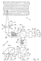
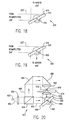
- Fig. 1 shows a schematic diagram of an optical data storage system of the present invention and is designated by the general reference number 10.
- System 10 includes an optical data storage medium 12 which is preferably disk shaped. Medium 12 removably mounted on a clamping spindle 14 as is known in the art. Spindle 14 is attached to a spindle motor 16 which in turn is attached to a system chassis 20. Motor 16 rotates spindle 14 and medium 12.
- An optical head 22 is positioned below medium 12. Head 22 is attached to an arm 24 which in turn is connected to an actuator device, such as a voice coil motor 26. Voice coil motor 26 is attached to chassis 20. Motor 26 moves arm 24 and head 22 in a radial direction below medium 12.
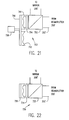
- Fig. 2A is a cross-sectional view of medium 12.
- Medium 12 has a substrate 50.
- Substrate 50 is also known as the face plate or cover plate and is where the laser beam enters medium 12.
- An outer diameter (OD) rim 52 and an inner diameter (ID) rim 54 are attached between face plate 50 and a substrate. 56.
- An OD rim 58 and an ID rim 60 are attached between substrate 56 and substrate 62.
- An OD rim 64 and an ID rim 66 are attached between substrates 62 and a substrate 68.
- An OD rim 70 and ID rim 72 are attached between substrates 68 and a substrate 74.
- Face plate 50 and substrates 56, 62, 68 and 74 are made of a light transmissive material such as glass, polycarbonate or other polymer material.
- face plate 50 is 1.2 mm thick and substrates 56, 62, 68 and 74 are 0.4 mm thick.
- the substrate may alternatively have thicknesses of 0.2 to 0.8 mm.
- the ID and OD rims are preferably made of a plastic material and are approximately 500 microns thick. The rims may alternatively have thicknesses of 50-500 microns.
- the rims may be attached to the face. plate and substrates by means of glue, cement or other bonding process.
- the rims may alternatively be integrally formed in the substrates. When in place, the rims form a plurality of annular spaces 78 between the substrates and the face plate.
- a spindle aperture 80 passes through medium 12 inside the ID rims for receiving the spindle 14.
- a plurality of passages 82 are provided in the ID rims connecting the aperture and the spaces 78 to allow pressure equalisation between the spaces 78 and the surrounding environment of the disk file, which would typically be air.
- a plurality of low impedance filters 84 are attached to passages 82 to prevent contamination of spaces 78 by particulate matter in the air. Filters 84 may be quartz or glass fibre. Passages 82 and filters 84 could alternatively be located on the OD rim.
- Surfaces 90, 92, 94, 96, 98, 100, 102 and 104 are data surfaces and lie adjacent spaces 78. These data surfaces may contain ROM data which is formed directly into the substrate surfaces or, alternatively the data surfaces may be coated with one of the various writeable optical storage films such as WORM, or one of the various erasable optical storage films such as phase change, or magneto-optical. Other than the optical storage films themselves, the data surfaces are made without the separate metallic reflector layer structures (reflectivity from 30-100%) which are known in the prior art such as US Patent 4,450,553.
- the data surfaces may comprise, consist of or essentially consist of the surface itself in the case of a ROM surface or the surface and an optical storage film in the case of WORM, phase change or magneto-optic surfaces.
- An additional nondata storing reflector layer is not needed. The result is that the data surfaces are very light transmissive and many data surfaces are possible.
- a reflector layer may optionally be added behind the last data surface 104 to achieve greater reflection from the last data surface 104.
- the data surfaces are ROM surfaces. Data is permanently recorded as pits which are formed directly into the substrate at the time the disk is manufactured.
- the ROM surfaces of the present invention do not have metallic reflector layers. The substrates have no coatings. The result is that the transmissivity of each data surface is approximately 96%. The 4% reflectivity is sufficient to detect the data.
- the high transmissivity has the benefit of allowing a large number of data surfaces to be accessed and minimises the effects of unwanted signals from other surfaces. Since there are no coatings on these surfaces, they are easier to manufacture and are more resistant to corrosion.
- One way to increase the reflectivity above 4% is to apply a thin film coating of a dielectric which has an index of refraction greater than the substrate.
- the maximum reflectivity of 20% occurs at a dielectric thickness of approximately ⁇ /4n, and varies monotonically to a minimum reflectivity of 4% at a thickness of approximately ⁇ /2n, where ⁇ / is the wavelength of the light and n is the index of refraction of the dielectric.
- dielectric materials are ZrO2, ZnS, SiNx or mixed oxides.
- the dielectric may be deposited by sputtering as is known in the art.
- the reflectivity of the data layer can also be reduced below 4%. This increases the transmittance and allows more disks to be stacked.
- the reduction in reflectivity occurs when a dielectric film which has an index of refraction less than the substrate is used.
- MnF which has a index of refraction of 1.35.
- the minimum reflectivity of 1% occurs at a dielectric thickness of approximately ⁇ /4n, and varies monotonically to a maximum reflectivity of 4% at a thickness of approximately ⁇ /2n, where ⁇ / is the wavelength of the light and n is the index of refraction.
- thin film anti-reflection materials which could also be used. These anti-reflection films may be applied by sputtering processes as are known in the art.
- the data surfaces may alternatively contain WORM data.
- WORM films such as tellurium-selenium alloys or phase change WORM films may be coated onto the data surfaces.
- the films are vacuum deposited by sputtering or evaporation onto the substrate as is known in the art. The amount of reflection, absorption, and transmission of each film is related to its thickness and optical constants.
- tellurium-selenium alloy is deposited at a thickness of 20-800 Angstroms.
- the data surface may alternatively contain reversible phase change films.
- Any type of phase change films may be used, however, preferred compositions include those that lie along or close to the tieline connecting GeTe and Sb2 Te3, which include Te 52.5 Ge 15.3 Sb33, Ge 2 Sb2 Te5, GeSb2 Te4 and GeSb 4 Te7.
- the films are vacuum deposited by sputtering processes as are known in the art onto the substrate to a thickness between 20-800 Angstroms.
- An optional protective overcoat of 3,000 Angstroms of dielectric may be formed on top of the phase change film in order to help prevent ablation.
- Data surfaces may also alternatively contain magneto-optical films.
- Magneto-optical film such as rare earth transition metals are vacuum deposited by sputtering processes as are known in the art onto the substrate to a thickness of 20-800 Angstroms.
- a further alternative is to have the data surfaces contain a combination of ROM, WORM, or erasable media.
- the higher transmission surfaces such as ROM are preferably located closer to the light source and the lower transmission surfaces such as WORM, phase change and magneto-optical are preferably located furthest away.
- the dielectric and anti-reflection films described above with the ROM surface may also be used with WORM and erasable media.
- Fig. 2B is a cross-sectional view of an alternative embodiment of an optical recording medium and is designated by the general reference number 120.
- Elements of medium 120 which are similar to elements of medium 12 are designated by a prime number.
- Medium 120 does not have the rims and spaces 78 of medium 12. Instead, a plurality of solid transparent members 122 separates the substrates.
- Members 122 are made of a material having a different index of refraction than the substrates. This is necessary to achieve some reflection at the data surfaces.
- the members 122 are made of an optical cement which also serves to hold the substrate together.
- the thickness of members 122 is preferably approximately 100-300 microns.
- Medium 120 may be substituted for medium 12 in system 10.
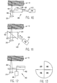
- Fig. 3A shows an exaggerated detailed cross-sectional view of a preferred data surface pattern of medium 12 and is designated by the general reference number 130.
- Surface 90 contains a pattern of spiral (or alternatively concentric) tracking grooves 132. The portions of surface 90 located between the grooves 132 are known as the land portions 134.
- Surface 92 contains a pattern of spiral inverse tracking grooves (raised ridges) 136. The portion of surface 92 located between the inverse grooves 136 is the land 138.
- the grooves 132 and the inverse grooves 136 are also referred to as tracking marks.
- the tracking marks are used to keep the light beam on track while the medium 12 rotates. This is described in more detail below.
- a beam 144 from the optical head 22 will track on the land portion 134 or 138 depending upon which surface it is focused upon.
- the recorded data is on the land portions.
- the tracking errors signal (TES) In order for the tracking errors signal (TES) to be of equal magnitude for both surfaces 90 and 92 the optical path difference between light reflected from the lands and tracking marks must be the same for both surfaces. Beam 144 focuses on surface 90 through substrate 50, however, beam 144 focuses on surface 92 through space 78. In the preferred embodiment space 78 contains air though it may contain another gas.
- d1n1 For the optical path length difference between the lands and tracking marks to be the same d1n1 must equal d2n2 (or d2/d1 equals n1/n2), where d1 is the depth of mark 132 (perpendicular distance), n1 is the index of refraction of substrate 50, d2 is the height of mark 136 (perpendicular distance), and n2 is the index of refraction of space 78.
- space 78 contains air which has an index of refraction of 1.0 and substrate 50 (as well as the other substrates) has an index of refraction 1.5. So the ratio of d2/d1 equals 1.5.
- d1 is 700 Angstroms and d2 is 1050 Angstroms.
- the same pattern of tracking marks is repeated on the other surfaces of medium 12.
- the other substrate incident surfaces 94, 98 and 102 are similar to surface 90 and the other space incident surfaces 96, 100 and 104 are similar to surface 92.
- the tracking marks are preferably arranged in a spiral pattern, they may alternatively be in a concentric pattern.
- the spiral pattern may be the same for each data surface, i.e., they are all clockwise or counter-clockwise spirals, or they may alternate between clockwise and counter-clockwise spiral patterns on consecutive data layers. This alternating spiral pattern may be preferable for certain applications, such as storage of video data, movies for example, where continuous tracking of data is desired.
- the beam tracks the clockwise spiral pattern inward on the first data surface until the spiral pattern ends near the inner diameter, and then the beam is refocused on the second data surface directly below and then the beam tracks the counter-clockwise spiral pattern outward until the outer diameter is reached.
- Fig. 3B shows an exaggerated detailed cross-sectional view of an alternative surface pattern for medium 12 and is designated by the general reference number 150.
- Pattern 150 is similar to pattern 130 except that the tracking marks or surface 92 are grooves 152 instead of inverse grooves.
- the pitch and the ratio of d2/d1 are the same as for pattern 130.
- Beam 144 will track on land 134 on surface 90, but now beam 144 will track on groove 152 when focused on surface 92. Tracking in the groove 132 may be desirable in certain situations. However, as will be described below, beam 144 may also be electronically controlled to track on land 138 of surface 92.
- the tracking marks for surfaces 94, 98 and 102 are similar to surface 90 and the surfaces 96, 100 and 104 are similar to surface 92.
- Fig. 3C shows an exaggerated detailed cross-sectional view of an alternative surface pattern for medium 12 which is designated by the general reference number 160.
- Pattern 160 is similar to pattern 130 except that surface 90 has inverse grooves 162 instead of grooves 132, and surface 92 has grooves 164 instead of inverse grooves 136.
- the pitch and ratio of d2/d1 are the same as for pattern 130.
- Beam 144 will track on inverse grooves 162 when focused on surface 90 and will track on grooves 164 when focused on surface 92(unless it is electronically switched to track on the land).
- the pattern for surfaces 94, 98 and 102 are similar to surface 90 and the surfaces 96, 100 and 104 are similar to surface 92.
- Fig. 3D shows an exaggerated detailed cross-sectinal view of an alternative surface pattern designated by the general reference number 170.
- the surface 90 has a similar structure to surface 90 of pattern 160.
- Surface 92 has a similar structure to surface 92 of pattern 130.
- the pitch and ratio of d2/d1 is the same as for pattern 130.
- Beam 144 will track on inverse grooves 162 when focused on surface 90 (unless it is electronically switched to track on the land) and will track on land 138 when focused on surface 92.
- Surfaces 94, 98 and 102 have similar patterns to surface 90 and surfaces 96, 100 and 104 have patterns similar to surface 92.
- the tracking marks are formed into the substrate at the time of manufacture by injection molding or photopolymer processes as are known in the art. It should be noted that the optical films, as described above, are deposited onto the substrates after the tracking marks are formed.
- tracking marks is also applicable to other features of optical disks.
- some ROM disks use pits embossed in the substrate to record data and/or provide tracking information.
- Other optical media use pits to emboss sector header information. Some media use these header pits to also provide tracking information.
- the pits are formed as pits or inverse pits on the various data surfaces corresponding in a similar manner to the tracking marks discussed above.
- the optical path length between the lands and the pits or inverse pits is also similar to the tracking marks.
- the pits, inverse pits, grooves and inverse grooves are all located at a different elevation from the land (i.e. the perpendicular distance between them and the land), and are all referred to as marks for purposes of this discussion. Marks which are specifically dedicated to providing tracking information are known as nondata tracking marks.
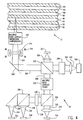
- Fig. 4 shows a schematic diagram of an optical head 22 and medium 12.
- Optical head 22 has a laser diode 200.
- Laser 200 may be a gallium-aluminum-arsenide diode laser which produces a primary beam of light 202 at approximately 780 nanometers wavelength.
- Beam 202 is collimated by lens 203 and is circularised by a circulariser 204 which may be a circularising prism.
- Beam 202 passes to a beamsplitter 205.
- a portion of beam 202 is reflected by beamsplitter 205 to a focus lens 206 and an optical detector 207.
- Detector 207 is used to monitor the power of beam 202.
- the rest of beam 202 passes to and is reflected by a mirror 208.
- Beam 202 then passes through a focus lens 210 and a multiple data surface aberration compensator 212 and is focused onto one of the data surfaces (surface 96 as shown) of medium 12.
- Lens 210 is mounted in a holder 214.
- the position of holder 214 is adjusted relative to medium 12 by a focus actuator motor 216 which may be a voice coil motor.
- a portion of the light beam 202 is reflected at the data surface as a reflected beam 220.
- Beam 220 returns through compensator 212 and lens 210 and is reflected by mirror 208.
- beam 220 is reflected to a multiple data surface filter 222.
- the beam 220 passes through filter 222 and passes to a beamsplitter 224.
- a first portion 230 of beam 220 is directed to an astigmatic lens 232 and a quad optical detector 234.
- a second portion 236 of beam 220 is directed through a half-wave plate 238 to a polarizing beamsplitter 240.
- Beamsplitter 240 separates light beam 236 into a first orthogonal polarized light component 242 and a second orthogonal polarized light component 244.
- a lens 246 focuses light 242 to an optical detector 248 and a lens 250 focuses light 244 to an optical detector 252.
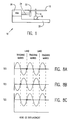
- Fig. 5 shows a top view of a quad detector 234.
- the detector 234 is divided into four equal sections 234A, B, C and D.
- Circuit 260 comprises a data circuit 262, a focus error circuit 264 and a tracking error circuit 266.
- Data circuit 262 has an amplifier 270 connected to detector 248 and an amplifier 272 connected to detector 252.
- Amplifiers 270 and 272 are connected to a double pole, double throw electronic switch 274.
- Switch 274 is connected to a summing amplifier 276 and a differential amplifier 278.
- Circuit 264 has a plurality of amplifiers 280, 282, 284 and 286 connected to detector sections 234A, B, C and D, respectively.
- a summing amplifier 288 is connected to amplifiers 280 and 284, and a summing amplifier 290 is connected to amplifiers 282 and 286.
- a differential amplifier 292 is connected to summing amplifiers 288 and 290.
- Circuit 266 has a pair of summing amplifiers 294 and 296, and a differential amplifier 298.
- Summing amplifier 294 is connected to amplifiers 280 and 282, and summing amplifier 296 is connected to amplifiers 284 and 286.
- Differential amplifier 298 is connected to summing amplifiers 294 and 296 via a double pole double throw electronic switch 297. Switch 297 acts to invert the inputs to amplifier 298.
- Fig. 7 is a schematic diagram of a controller system of the present invention and is designated by the general reference number 300.
- a focus error signal (FES) peak detector 310 is connected to the focus error signal circuit 264.
- a track error signal (TES) peak detector 312 is connected to the tracking error signal circuit 266.
- a controller 314 is connected to detector 310, detector 312, detector 207 and circuits 262, 264 and 266.
- Controller 314 is a microprocessor based disk drive controller. Controller 314 is also connected to and controls the laser 200, head motor 26, spindle motor 16, focus motor 216, switches 274 and 297, and compensator 212. The exact configuration and operation of compensator 212 is described in more detail below.
- Controller 314 causes motor 16 to rotate disk 12 and causes motor 26 to move head 22 to the proper position below disk 12. See Fig. 4.
- Laser 200 is energized to read data from disk 12.
- the beam 202 is focused by lens 210 on the data surface 96.
- the reflected beam 220 returns and is divided into beams 230, 242 and 244.
- Beam 230 is detected by detector 234 and is used to provide focus and tracking servo information
- beams 242 and 244 are detected by detectors 248 and 252, respectively, and are used to provide data signals.
- beam 202 is focused exactly on a track of data surface 96, then beam 230 will fall as a circular cross-section 350 equally between the sections A and B, and the sections D and C. If the beam is off track it will fall on the boundary between a tracking mark and the land. The result is that the beam is diffracted and cross-section 350 will move up or down. More light will be received by sections A and B, and less by sections C and D or vice versa.
- Fig. 8A shows a graph of the TES produced by circuit 264 versus the displacement of head 22.
- Controller 314 causes VCM 26 to move head 22 across the surface of medium 12.
- TES peak detector 312 counts the peaks (maximum and minimum points) of the TES signals. There are two peaks between each track. By counting the number of peaks, controller 314 is able to position the beam on the proper track.
- the TES signal at a land is a positive slope TES signal. Controller 314 uses this positive slope signal to lock the beam on track. For example, a positive TES signal causes head 22 to move to the left toward the zero point land position and a negative TES signal causes the head 22 to move to the right toward the zero point land position.
- 8A is the signal derived from the preferred pattern 130 of medium 12 when switch 297 is in its initial position as shown in Fig. 6. The same signal is also generated for surface 90 of pattern 150, and surface 92 of pattern 170. The beam is automatically locked to the land because that is the position where there is a positive slope.
- Fig. 8B shows a graph of the TES versus head displacement for surface 92 of pattern 150, surfaces 90 and 92 of pattern 160 and surface 90 of pattern 170 when switch 297 is in its initial position.
- the tracking marks are such that the positive slope signal occurs at the location of the tracking marks and so that the beam will automatically track on the tracking marks and not the land portions. Tracking on the tracking marks may be desirable in some circumstances.
- Fig. 8C shows a graph of the TES versus head displacement for surface 92 of pattern 150, surfaces 90 and 92 of pattern 160 and surface 90 of pattern 170 when inverter switch 297 is enabled such that the TES signal is inverted.
- the TES now has a positive slope at the land positions and the beam will track on the land portion instead of the tracking marks.
- controller 314 can track the grooves or the lands by setting switch 297.
- medium 12 contains ROM data surfaces. Reflectivity detection is used to read the ROM data.
- switch 274 is positioned to connect amplifier 276 when a ROM disk is to be read. The signal from detectors 248 and 252 is added. Less light is detected where data spots have been recorded and this difference in light detected is the data signal. Switch 274 will have the same setting for reading WORM and phase change data disk. If disk 12 has magneto-optical data surfaces, then polarization detection is needed to read the data. Switch 274 will be set to connect amplifier 278. The difference in the orthogonal polarization light detected at detectors 248 and 252 will then provide the data signal.
- Fig. 9 shows a graph of the focus error signal from circuit 264 versus the displacement distance of lens 210. Note that a nominally sinusoidal focus error signal is obtained for each of the data surfaces of medium 12. Between the data layers, the focus error signal is zero.
- controller 314 first causes motor 216 to position lens 210 at its zero displacement position. Controller 314 will then seek the desired data surface by causing motor 216 to move lens 210 in a positive displacement direction. At each data layer, peak detector 310 will detect the two peaks of the focus error signal. Controller 314 will count the peaks (two per data surface) and determine the exact data surface on which beam 202 is focused.
- controller 314 When the desired surfaces are reached, controller 314 causes motor 216 to position lens 210 such that the focus error signal is between the two peaks for that particular data surface. The focus error is then used to control the motor 216 to seek the zero point focus error signal between the peaks, i.e. lock on the positive slope signal such that exact focus is achieved.
- the controller 314 will also adjust the power of laser 200, the switch 297, and the aberration compensator 212 as appropriate for that particular data surface.
- controller 314 determines what type of disk it is reading.
- Switch 274 is first positioned for reflectivity detection and switch 297 is set to read the land portions of the disk of the preferred pattern 130.
- the controller 314 seeks and reads the header information of the first track of the first data surface.
- the header has information on the number of layers, what type of optical media is in each layer (reflectivity or polarization detection), and what type of tracking mark patterns are used. With this information, the controller 314 is able to set switches 274 and 297 to correctly read each data surface.
- the disk may have four layers of ROM data surfaces and two layers of MO data surfaces. Controller 314 will set switch 274 to reflectivity detection for surfaces 1-4 and to polarization detection for surfaces 5-6.
- controller 314 If controller 314 is unable to read the first track of the first data surface (perhaps the first layer has a different tracking mark pattern), then controller 314 will set switch 297 to its other setting and will attempt to read the first track of the first data surface again. If this still does not work (perhaps the first data surface is magneto-optic and requires polarization detection) then the controller will set switch 274 to the polarization detection and try again, setting switch 297 at one setting and then the other. In summary, controller 314 will read the header information of the first track of the first data surface by trying the four different combinations of settings of switches 274 and 297 until it is successful at reading the track. Once controller 314 has this header information, it can correctly set the switches 274 and 297 for each of the other data surfaces.
- the disk drive may be specifically dedicated to work with only one type of medium.
- controller 314 is preprogrammed to store information on the type of data surfaces, number of layers, and types of tracking marks.
- Lenses are typically designed to focus light through air which has an index of refraction of 1.0. When such lenses focus light through materials having different indices of refraction, the light experiences a spherical aberration, which distorts and enlarges the beam spot, degrading the reading and recording performance.
- NA numerical aperture
- FIG. 10 shows a schematic diagram of an aberration compensator which is designated by the general reference number 400 and may be used as compensator 212.
- Compensator 400 comprises a stepped block 402 having three steps.
- a first step 404 has a thickness of 0.4 mm
- a second step 406 has a thickness of 0.8 mm
- a third step 408 has a thickness of 1.2 mm.
- the block 402 is made of the same material as the face plate and substrates of medium 12 or other similar optical material. Note that these steps increase in optical thickness in increments of the substrate thickness.
- Block 402 is attached to a voice coil motor 410 (or similar actuator device) which in turn is connected to controller 314. Motor 410 moves block 402 laterally into and out of the path of beam 302.
- Lens 210 is designed to focus on the lowest data surface of medium 12.
- lens 210 is designed to compensate for spherical aberrations caused by the combined thicknesses of the face plate and the intervening substrates.
- beam 202 in order to focus on surface 102 or 104, beam 202 must pass through the face plate 50 and substrates 56, 62 and 68 (a combined thickness of 2.4 mm of the substrate material). Note that the air spaces 78 are not counted because they impart no additional spherical aberration.
- Lens 210 is thus designed to focus through 2.4 mm of polycarbonate and may focus equally well on both data surfaces 102 and 104.
- Fig. 11 shows an aberration compensator which is designated by the general reference number 430 and which may be used for compensator 212.
- Compensator 430 has a pair of complementary triangular shaped blocks 432 and 434.
- Blocks 432 and 434 are made of the same material as face plate and substrates of medium 12 or material of similar optical properties.
- Block 432 is positioned in a fixed position such that beam 202 passes through it.
- Block 434 is attached to a voice coil motor 436 and may be slid along the surface of block 432.
- Controller 314 is connected to and controls motor 436. By moving block 434 relative to block 432 the overall thickness of material through which beam 202 passes may be adjusted. The result is that beam 202 passes through the same optical thickness of material no matter which data surface it is focused on.
- Figs. 12 and 13 show an aberration compensator which is designated by the general reference number 450 and may be used for compensator 212.
- Compensator 450 has a circular stepped element 452.
- Element 452 has four sections 454, 456, 458 and 460. Sections 456, 458 and 460 have thicknesses similar to steps 404, 406 and 408, respectively, of compensator 400.
- Section 454 has no material and represents a blank space in the circular pattern as shown in Fig. 13.
- the circular element 452 is attached to a stepper motor 462 which in turn is controlled by controller 314. Spindle 462 rotates element 452 such that beam 202 passes through the same thickness of material no matter which data surface it is focused on.
- Fig. 14 shows an aberration compensator which is designated by the general reference number 570 and may be used for compensator 212.
- Compensator 570 comprises a stationary convex lens 572 and a moveable concave lens 574.
- Lens 574 is attached to a voice coil motor 576.
- Voice coil motor 576 is controlled by controller 314 to move lens 574 relative to lens 572.
- Beam 202 passes through lens 572, lens 574 and lens 210 to medium 12. Moving lens 574 relative to lens 572 changes the spherical aberration of beam 202 and allows it to focus on the different data surfaces.
- lenses 210, 574 and 572 comprise a Cooke triplet having movable center element 574.
- Fig. 15 shows an aberration compensator which is designated by the general reference number 580.
- Compensator 580 comprises an aspheric lens element 582 with nominally zero focal power.
- Element 582 has a spherical aberration surface 584 and a planar surface 586.
- Lens 582 is connected to a voice coil motor 588.
- Voice coil motor 588 is controlled by controller 314 which moves lens 582 relative to lens 512.
- Beam 202 passes through lens 210 and lens 582 to medium 12. Moving lens 582 relative to lens 210 changes the spherical aberration of the beam 202 and allows it to focus on the different data surfaces.
- Fig. 16 shows a view of lens 582 relative to axes z and p.
- Fig. 17 shows a schematic diagram of an alternative optical head of the present invention and is designated by the general reference number 600.
- Elements of head 600 which are similar to elements of head 22 are designate by a prime number.
- head 600 is similar to system 10 except that the aberration compensator 212 has been eliminated and a new aberration compensator 602 has been added between beamsplitter 206′ and mirror 208′. The description and operation of compensator 602 is described below.
- the operation of head 600 is otherwise the same as described for head 22. Head 600 may be substituted for head 22 in system 10.
- Fig. 18 shows a schematic diagram of an aberration compensator which is designated by the general reference number 610 and may be used for compensator 602.
- Compensator 610 comprises a substrate 612 having a reflective holographic coating 614.
- Substrate 612 is attached to a stepper motor 616 which in turn is controlled by controller 314.
- Holographic coating 614 has a number of different holograms recorded, each of which imparts a particular spherical aberration to beam 202′. These holograms are of the Bragg type which are sensitive only to light incident at a specific angle and wavelength.
- beam 202′ will experience a different hologram.
- the number of holograms recorded corresponds to the number of different spherical aberration corrections required. For medium 12 as shown, four different recordings are necessary each corresponding to one of the pairs of data surfaces.
- Fig. 19 shows a schematic diagram of an aberration compensator which is designated by the general reference number 620 and may be used for compensator 602.
- Compensator 620 comprises a substrate 622, a transmissive holographic coating 624 and a stepper motor 626.
- the compensator 620 is similar to compensator 610 except that here the holographic coating 624 is transmissive rather than reflective.
- Holographic coating 624 has a number of holograms recorded, each of which corresponds to the amount of spherical aberration compensation required. Beam 202′ experiences each of these holograms in turn as substrate 622 is rotated.
- Fig. 20 shows a schematic diagram of a recording system used to make the holographic coatings 614 and 624, and is designated by the general reference number 650.
- System 650 has a laser 652 which produces a light beam 654 at a frequency similar to the laser 200.
- Light 654 is collimated by lens 656 and is passed to a beamsplitter 658.
- Beamsplitter 658 divides the light into a beam 660 and a beam 662.
- Beam 660 is reflected by a mirror 664 and 666, and is focused by a lens 668 to a point 670 in a plane 672.
- Beam 660 passes through a stepped block 674 similar to block 402.
- Beam 660 is then recollimated by a lens 676 and falls upon a holographic coating 680 on a substrate 682.
- Substrate 682 is rotatably mounted to a stepper motor 684.
- Beam 662 also falls upon coating 680 at a 90 degree angle from beam 660.
- Lens 668 forms an unaberrated spot on plane 672.
- This light is then passed through a step of block 674 which has a thickness representing the sum of the substrate thicknesses which will be encountered in accessing a particular recording layer.
- Lens 676 is identical in design to lens 210 as used in the optical storage head. It collimates the light into a beam that contains a specific amount of spherical aberration corresponding to the specific thickness.
- This wavefront is holographically recorded by interference with the reference beam 662. If the hologram is oriented in approximately a plane 690 as shown, a transmission hologram is recorded. If it is oriented in approximately a plane 692 as shown as a dash line, a reflective hologram is recorded.
- the wavefront required to correct the aberrations encountered in accessing a different pair of recording layers is holographically stored by rotating the hologram to a new angular position and inserting the corresponding thickness plate of block 674.
- a multiplicity of angularly resolved holograms are recorded, each corresponding to and providing correction for a different pair of recording layers.
- the holographic coating may be made of dichromated gelatin or a photopolymer material.
- the individual holograms can be recorded in increments as small as one degree without appreciable cross-talk. This permits large numbers of holograms to be recorded and correspondingly large numbers of data surfaces to be used.
- Fig. 21 shows a schematic diagram of an alternative aberration compensator which is designated by the general reference number 700 and may be used for compensator 602.
- Compensator 700 comprises a polarizing beamsplitter 702, a quarter waveplate 704, a carousel 706 attached to a stepper motor 708 and a plurality of spherical aberration mirrors 710 each providing a different spherical aberration correction.
- Beam 202′ is oriented with its polarization such that it passes through beamsplitter 702 and plate 704 to one of mirrors 710.
- Mirror 710 imparts the appropriate spherical aberration to the beam 202′ which then returns through plate 704 and is reflected by beamsplitter 702 to mirror 208′.
- Motor 708 is controlled by controller 314 to rotate the carousel 706 to position the appropriate mirror in place.
- Mirrors 710 are reflecting Schmidt corrector plates. See M. Born, et al., “Principles of Optics,” Pergonan Press Oxford, 1975, pp. 245-249.
- Fig. 22 shows a schematic diagram of an aberration compensator which is designated by the general reference number 720 and may be used for compensator 602.
- Compensator 720 comprises a polarizing beamsplitter 722, a quarter waveplate 724 and an electrical controlled deformable mirror 726.
- Deformable mirror 726 is controlled by internal piezo-electric elements and is described in more detail in J.P. Gaffarel, et al., "Applied Optics," Vol. 26, pp. 3772-3777, (1987).
- the operation of compensator 720 is similar to compensator 700, except that mirror 726 is electrically adjusted to provide the appropriate spherical aberration. In other words, mirror 726 is adjusted to form a reflective surface corresponding to the different Schmidt corrector plates 710 of compensator 700. Controller 314 controls the adjustment of mirror 726 as appropriate.
- aberration compensators 212 and 602 have been described above in connection with medium 12. Due to the air space between the layers, one aberration compensation setting will work for each pair of data surfaces. However, in the case where medium 120 is used, aberration compensation settings will need to be made for each data surface. This is because there are no air spaces.
- reflected beam 230 is returned to head 22 from that surface.
- some of light beam 202 is also reflected at the other data surfaces. This unwanted reflected light must be screened out for proper data and servo signals to be obtained.
- the multiple data surface filter 222 of the present invention achieves this function.
- Fig. 23 shows a schematic diagram of a filter 750 which may be used as filter 222.
- Filter 750 comprises a blocking plate 754 and a lens 756.
- the desired light beam 230 is collimated because it is the light which has been properly focused by lens 210.
- Beam 230 is focused by lens 752 to a point 760.
- Unwanted light 762 is not properly focused by lens 210 and is thus not collimated.
- the light 762 will not focus to point 760.
- Plate 764 has an aperture 764 at point 760 which allows light 230 to pass. Most of the unwanted light 762 is blocked by plate 754.
- the light 230 is recollimated by lens 756.
- aperture 764 is circularly shaped and has a diameter of approximately ⁇ /(2*(NA)), where ⁇ / is the wavelength of the light and N.A. is the numerical aperture of lens 752. The exact diameter is determined by the desired trade-off between alignment tolerances and interlayer signal rejection requirements.
- aperture 764 may be a slit having a minimum gap distance of approximately ⁇ /(2*(NA)). In such a case plate 764 could be two separate members which are separated by the slit.
- Plate 754 may be made of a metal sheet or may be made of a transparent substrate having a light blocking coating with aperture 764 being uncoated.
- Fig. 24 shows a schematic diagram of a filter 800 which also may be used as filter 222.
- Filter 800 comprises a lens 802, a blocking plate 804, a blocking plate 806 and a lens 808.
- Plate 806 has an aperture 810 located at a focal point 812 of lens 802.
- Plate 804 has a complementary aperture 814 which allows the collimated light 230 to be directed through aperture 810 while locking unwanted uncollimated light 820.
- Aperture 814 may be a pair of parallel slits or an annular aperture. In a preferred embodiment, the distance between the slits of aperture 814 is greater than the diameter of aperture 810.
- the diameter of aperture 810 is approximately equal to ⁇ /(2*(NA)).
- Blocking plates 804 and 806 may be made of a metal sheet or may be made of a transparent substrate having a light blocking coating with apertures 810 and 814 being uncoated.
- Fig. 25 shows a schematic diagram of an alternative filter 830 which may be used as filter 222.
- Filter 830 comprises a beamsplitter 832 and a holographic plate 834.
- the coating on the holographic plate 834 is tuned to efficiently reflect collimated beam 230 while uncollimated beam 840 is allowed to pass.
- the desired beam 230 is reflected from holographic plate 834 and returns to beamsplitter 832 where it is reflected towards beamsplitter 224.
- Fig. 26 is a schematic diagram which shows hows how holographic plate 834 is made.
- a collimated laser beam 850 having approximately the same wavelength as laser 200 is split into two beams 852 and 854 at an amplitude beamsplitter 856.
- Beams 852 and 854 are directed by mirrors 860 and 862, respectively, and fall upon hologram plate 834 from opposite directions perpendicular to the surface of plate 834.
- a reflective hologram is recorded by the interference of beams 852 and 854.
- the holographic coating may be made of a dichromated gel or photopolymer material.
- Filters 222 of the present invention have been shown in Fig. 4 to be located in the path of beam 220. However, one or more filters can be located in the separate paths of servo beam 230 or the data beam 236.
Abstract
Description
- This invention relates generally to optical data storage systems and more specifically to a storage system having multiple data storage surfaces.
- Optical data storage systems provide a means for storing great quantities of data on a disk. The data is accessed by focusing a laser beam onto the data layer of the disk and then detecting the reflected light beam. Various kinds of systems are known. In a ROM (Read Only Memory) system, data is permanently embedded as marks in the disk at the time of manufacture of the disk. The data is detected as a change in reflectivity as the laser beam passes over the data marks. A WORM (Write-Once Read Many) system allows the user to write data by making marks, such as pits, on a blank optical disk surface. Once the data is recorded onto the disk it cannot be erased. The data in A WORM system is also detected as a change in reflectivity.
- Erasable optical systems are also known. These systems use the laser to heat the data layer above a critical temperature in order to write and erase the data. Magneto-optical recording systems record data by orienting the magnetic domain of a spot in either an up or a down position. The data is read by directing a low power laser to the data layer. The differences in magnetic domain direction cause the plane of polarisation of the light beam to be rotated one way or the other, clockwise or counterclockwise. This change in orientation of polarisation is then detected. Phase change recording uses a structural change of the data layer itself (amorphous/crystalline are two common types of phases) to record the data. The data is detected as changes in reflectivity as a beam passes over the different phases.
- In order to increase the storage capacity of an optical disk, multiple data layer systems have been proposed. An optical disk having two or more data layers may in theory be accessed at different layers by changing the focal position of the lens. Examples of this approach include US Patent 3,946,367 issued March 23, 1976 by Wohlmut, et al.; US Patent 4,219,704 issued August 26, 1980 to Russell; US Patent 4,450,553 issued May 22, 1984 to Holster, et al.; US 4,905,215 issued February 27, 1990 to Hattori, et al.; Japanese Published Application, 63-276732 published November 15, 1988 by Watanabe, et al.; and IBM Technical Disclosure Bulletin, Vol. 30, No. 2, p. 667, July 1987, by Arter, et al.
- The problem with these prior art systems has been that the ability to clearly read the data recorded is very difficult if there is more than one data layer. An optical data storage system is needed which overcomes this problem.
- Accordingly, the present invention provides, in one aspect, an optical data storage medium comprising: a first radiation transmissive member having a first data surface for storing recorded data, the first data surface having a land portion and nondata tracking marks at an elevation different from the land portion; a second member, spaced from the first member, having a second data surface for storing recorded data, the second data surface having a land portion and nondata tracking marks at an elevation different from the land portion; a radiation transmissive medium located between the first and second data surfaces through which a beam of radiation can pass from a first side of the medium to a focus on either the first or second data surface.
- Thus is provided a medium in which the first member, which would be closest the read laser when in position within a storage system, has a high transmissivity. This is in contrast to prior art media in which a reflector layer is provided with the first member in order that a significant proportion of the incident light is reflected.
- It will be appreciated that the medium of the present invention allows for the transmission of a high percentage of the light incident on the first member to the second member. Thus the medium may include a larger number of data layers than is practicable in prior art systems.
- In a second aspect of the invention there is provided an optical data storage system incorporating such a multiple data surface optical medium. In a preferred system the medium has a plurality of substrate members separated by air spaces. The surfaces of the substrate members which are adjacent to the air spaces are the data surfaces. The data surfaces are highly transmissive with the exception of the last data layer which may include a reflector layer. Each data surface has tracking marks.
- Preferred embodiments of the invention will now be described, by way of example only, with reference to the accompanying drawings in which:
- Fig. 1 is a schematic diagram of an optical data storage system;
- Fig. 2A is a cross-sectional view of an optical medium according to the present invention;
- Fig. 2B is a cross-sectional view of an alternative optical medium;
- Fig. 3A is a cross-sectional view of the tracking marks of the medium of Fig. 2;
- Fig. 3B is a cross-sectional view of alternative tracking marks;
- Fig. 3C is a cross-sectional view of alternative tracking marks;
- Fig. 3D is a cross-sectional view of alternative tracking marks;
- Fig. 4 is a schematic diagram of an optical head and medium;
- Fig. 5 is a top view of an optical detector of Fig. 4;
- Fig. 6 is a circuit diagram of a channel circuit;
- Fig. 7 is a schematic diagram of a controller circuit;
- Fig. 8A is a graph of tracking error signal versus head displacement;
- Fig. 8B is a graph of tracking error signal versus head displacement for an alternative embodiment;
- Fig. 8C is a graph of tracking error signal versus head displacement for an alternative embodiment;
- Fig. 9 is a graph of the focus error signal versus lens displacement for the present invention;
- Fig. 10 is a schematic diagram of a multiple data surface aberration compensator;
- Fig. 11 is a schematic diagram of an alternative embodiment of a multiple data surface aberration compensator;
- Fig. 12 is a schematic diagram of an additional alternative embodiment of a multiple data surface aberration compensator;
- Fig. 13 is a top view of the compensator of Fig. 12;
- Fig. 14 is a schematic diagram of an additional alternative embodiment of a multiple data surface aberration compensator;
- Fig. 15 is a schematic diagram of an alternative embodiment of a multiple data surface aberration compensator;
- Fig. 16 is a cross-sectional view of the lens of Fig. 15;
- Fig. 17 is a schematic diagram of an alternative embodiment of an optical head and medium;
- Fig. 18 is a schematic diagram of an alternative embodiment of a multiple data surface aberration compensator;
- Fig. 19 is a schematic diagram of an alternative embodiment of a multiple data surface aberration compensator;
- Fig. 20 is a schematic diagram showing the process of manufacturing the compensator of Figs. 18 and 19;
- Fig. 21 is a schematic diagram of an alternative embodiment of the aberration compensator;
- Fig. 22 is a schematic diagram of an alternative embodiment of the aberration compensator;
- Fig. 23 is a schematic diagram of a multiple data surface filter;
- Fig. 24 is a schematic diagram of an alternative embodiment of a multiple data surface filter;
- Fig. 25 is a schematic diagram of an alternative embodiment of a multiple data surface filter; and
- Fig. 26 is a schematic diagram showing the process of manufacturing the filter of Fig. 25.
- Fig. 1 shows a schematic diagram of an optical data storage system of the present invention and is designated by the
general reference number 10.System 10 includes an opticaldata storage medium 12 which is preferably disk shaped.Medium 12 removably mounted on a clampingspindle 14 as is known in the art.Spindle 14 is attached to aspindle motor 16 which in turn is attached to asystem chassis 20.Motor 16 rotatesspindle 14 andmedium 12. - An
optical head 22 is positioned belowmedium 12.Head 22 is attached to anarm 24 which in turn is connected to an actuator device, such as avoice coil motor 26.Voice coil motor 26 is attached tochassis 20.Motor 26 movesarm 24 andhead 22 in a radial direction belowmedium 12. - Fig. 2A is a cross-sectional view of
medium 12.Medium 12 has asubstrate 50.Substrate 50 is also known as the face plate or cover plate and is where the laser beam entersmedium 12. An outer diameter (OD) rim 52 and an inner diameter (ID) rim 54 are attached betweenface plate 50 and a substrate. 56. AnOD rim 58 and anID rim 60 are attached betweensubstrate 56 andsubstrate 62. AnOD rim 64 and anID rim 66 are attached betweensubstrates 62 and asubstrate 68. AnOD rim 70 and ID rim 72 are attached betweensubstrates 68 and asubstrate 74.Face plate 50 andsubstrates face plate 50 is 1.2 mm thick andsubstrates - The rims may be attached to the face. plate and substrates by means of glue, cement or other bonding process. The rims may alternatively be integrally formed in the substrates. When in place, the rims form a plurality of
annular spaces 78 between the substrates and the face plate. Aspindle aperture 80 passes throughmedium 12 inside the ID rims for receiving thespindle 14. A plurality ofpassages 82 are provided in the ID rims connecting the aperture and thespaces 78 to allow pressure equalisation between thespaces 78 and the surrounding environment of the disk file, which would typically be air. A plurality oflow impedance filters 84 are attached topassages 82 to prevent contamination ofspaces 78 by particulate matter in the air.Filters 84 may be quartz or glass fibre.Passages 82 and filters 84 could alternatively be located on the OD rim. -
Surfaces adjacent spaces 78. These data surfaces may contain ROM data which is formed directly into the substrate surfaces or, alternatively the data surfaces may be coated with one of the various writeable optical storage films such as WORM, or one of the various erasable optical storage films such as phase change, or magneto-optical. Other than the optical storage films themselves, the data surfaces are made without the separate metallic reflector layer structures (reflectivity from 30-100%) which are known in the prior art such as US Patent 4,450,553. In other words, the data surfaces may comprise, consist of or essentially consist of the surface itself in the case of a ROM surface or the surface and an optical storage film in the case of WORM, phase change or magneto-optic surfaces. An additional nondata storing reflector layer is not needed. The result is that the data surfaces are very light transmissive and many data surfaces are possible. Although the intermediate data surfaces do not have reflector layers, a reflector layer may optionally be added behind thelast data surface 104 to achieve greater reflection from thelast data surface 104. - In the preferred embodiment, the data surfaces are ROM surfaces. Data is permanently recorded as pits which are formed directly into the substrate at the time the disk is manufactured. In contrast to the prior art, the ROM surfaces of the present invention do not have metallic reflector layers. The substrates have no coatings. The result is that the transmissivity of each data surface is approximately 96%. The 4% reflectivity is sufficient to detect the data. The high transmissivity has the benefit of allowing a large number of data surfaces to be accessed and minimises the effects of unwanted signals from other surfaces. Since there are no coatings on these surfaces, they are easier to manufacture and are more resistant to corrosion.
- Although it is not necessary, it may be desirable to increase the reflectivity to reduce the required laser power. One way to increase the reflectivity above 4% is to apply a thin film coating of a dielectric which has an index of refraction greater than the substrate. The maximum reflectivity of 20% occurs at a dielectric thickness of approximately λ/4n, and varies monotonically to a minimum reflectivity of 4% at a thickness of approximately λ/2n, where λ/ is the wavelength of the light and n is the index of refraction of the dielectric. Examples of such dielectric materials are ZrO₂, ZnS, SiNx or mixed oxides. The dielectric may be deposited by sputtering as is known in the art.
- The reflectivity of the data layer can also be reduced below 4%. This increases the transmittance and allows more disks to be stacked. The reduction in reflectivity occurs when a dielectric film which has an index of refraction less than the substrate is used. One such dielectric is MnF which has a index of refraction of 1.35. The minimum reflectivity of 1% occurs at a dielectric thickness of approximately λ/4n, and varies monotonically to a maximum reflectivity of 4% at a thickness of approximately λ/2n, where λ/ is the wavelength of the light and n is the index of refraction. There are many other thin film anti-reflection materials which could also be used. These anti-reflection films may be applied by sputtering processes as are known in the art.
- The data surfaces may alternatively contain WORM data. WORM films such as tellurium-selenium alloys or phase change WORM films may be coated onto the data surfaces. The films are vacuum deposited by sputtering or evaporation onto the substrate as is known in the art. The amount of reflection, absorption, and transmission of each film is related to its thickness and optical constants. In a preferred embodiment, tellurium-selenium alloy is deposited at a thickness of 20-800 Angstroms.
- The data surface may alternatively contain reversible phase change films. Any type of phase change films may be used, however, preferred compositions include those that lie along or close to the tieline connecting GeTe and Sb₂ Te₃, which include Te52.5 Ge15.3 Sb₃₃, Ge ₂ Sb₂ Te₅, GeSb₂ Te₄ and GeSb ₄ Te₇. The films are vacuum deposited by sputtering processes as are known in the art onto the substrate to a thickness between 20-800 Angstroms. An optional protective overcoat of 3,000 Angstroms of dielectric may be formed on top of the phase change film in order to help prevent ablation.
- Data surfaces may also alternatively contain magneto-optical films. Magneto-optical film such as rare earth transition metals are vacuum deposited by sputtering processes as are known in the art onto the substrate to a thickness of 20-800 Angstroms.
- A further alternative is to have the data surfaces contain a combination of ROM, WORM, or erasable media. The higher transmission surfaces such as ROM are preferably located closer to the light source and the lower transmission surfaces such as WORM, phase change and magneto-optical are preferably located furthest away. The dielectric and anti-reflection films described above with the ROM surface may also be used with WORM and erasable media.
- Fig. 2B is a cross-sectional view of an alternative embodiment of an optical recording medium and is designated by the
general reference number 120. Elements ofmedium 120 which are similar to elements ofmedium 12 are designated by a prime number.Medium 120 does not have the rims andspaces 78 ofmedium 12. Instead, a plurality of solidtransparent members 122 separates the substrates.Members 122 are made of a material having a different index of refraction than the substrates. This is necessary to achieve some reflection at the data surfaces. In a preferred embodiment, themembers 122 are made of an optical cement which also serves to hold the substrate together. The thickness ofmembers 122 is preferably approximately 100-300 microns.Medium 120 may be substituted formedium 12 insystem 10. - Fig. 3A shows an exaggerated detailed cross-sectional view of a preferred data surface pattern of
medium 12 and is designated by thegeneral reference number 130.Surface 90 contains a pattern of spiral (or alternatively concentric) trackinggrooves 132. The portions ofsurface 90 located between thegrooves 132 are known as theland portions 134.Surface 92 contains a pattern of spiral inverse tracking grooves (raised ridges) 136. The portion ofsurface 92 located between theinverse grooves 136 is theland 138. Thegrooves 132 and theinverse grooves 136 are also referred to as tracking marks. In a preferred embodiment, thewidths 140 of the tracking marks are 0.6 microns and thewidth 142 of the land sections is 1.0 microns. This results in a pitch of
- The tracking marks are used to keep the light beam on track while the medium 12 rotates. This is described in more detail below. For
pattern 130, abeam 144 from theoptical head 22 will track on theland portion surfaces Beam 144 focuses onsurface 90 throughsubstrate 50, however,beam 144 focuses onsurface 92 throughspace 78. In thepreferred embodiment space 78 contains air though it may contain another gas. For the optical path length difference between the lands and tracking marks to be the same d1n1 must equal d2n2 (or d2/d1 equals n1/n2), where d1 is the depth of mark 132 (perpendicular distance), n1 is the index of refraction ofsubstrate 50, d2 is the height of mark 136 (perpendicular distance), and n2 is the index of refraction ofspace 78. In a preferred embodiment,space 78 contains air which has an index of refraction of 1.0 and substrate 50 (as well as the other substrates) has an index of refraction 1.5. So the ratio of d2/d1 equals 1.5. In a preferred embodiment, d1 is 700 Angstroms and d2 is 1050 Angstroms. The same pattern of tracking marks is repeated on the other surfaces ofmedium 12. The other substrate incident surfaces 94, 98 and 102 are similar to surface 90 and the other space incident surfaces 96, 100 and 104 are similar tosurface 92. - Although the tracking marks are preferably arranged in a spiral pattern, they may alternatively be in a concentric pattern. In addition, the spiral pattern may be the same for each data surface, i.e., they are all clockwise or counter-clockwise spirals, or they may alternate between clockwise and counter-clockwise spiral patterns on consecutive data layers. This alternating spiral pattern may be preferable for certain applications, such as storage of video data, movies for example, where continuous tracking of data is desired. In such a case, the beam tracks the clockwise spiral pattern inward on the first data surface until the spiral pattern ends near the inner diameter, and then the beam is refocused on the second data surface directly below and then the beam tracks the counter-clockwise spiral pattern outward until the outer diameter is reached.
- Fig. 3B shows an exaggerated detailed cross-sectional view of an alternative surface pattern for
medium 12 and is designated by thegeneral reference number 150.Pattern 150 is similar topattern 130 except that the tracking marks orsurface 92 aregrooves 152 instead of inverse grooves. The pitch and the ratio of d2/d1 are the same as forpattern 130.Beam 144 will track onland 134 onsurface 90, but nowbeam 144 will track ongroove 152 when focused onsurface 92. Tracking in thegroove 132 may be desirable in certain situations. However, as will be described below,beam 144 may also be electronically controlled to track onland 138 ofsurface 92. The tracking marks forsurfaces surfaces surface 92. - Fig. 3C shows an exaggerated detailed cross-sectional view of an alternative surface pattern for
medium 12 which is designated by thegeneral reference number 160.Pattern 160 is similar topattern 130 except thatsurface 90 hasinverse grooves 162 instead ofgrooves 132, andsurface 92 hasgrooves 164 instead ofinverse grooves 136. The pitch and ratio of d2/d1 are the same as forpattern 130.Beam 144 will track oninverse grooves 162 when focused onsurface 90 and will track ongrooves 164 when focused on surface 92(unless it is electronically switched to track on the land). The pattern forsurfaces surfaces surface 92. - Fig. 3D shows an exaggerated detailed cross-sectinal view of an alternative surface pattern designated by the
general reference number 170. Inpattern 170, thesurface 90 has a similar structure to surface 90 ofpattern 160.Surface 92 has a similar structure to surface 92 ofpattern 130. The pitch and ratio of d2/d1 is the same as forpattern 130.Beam 144 will track oninverse grooves 162 when focused on surface 90 (unless it is electronically switched to track on the land) and will track onland 138 when focused onsurface 92.Surfaces surface 92. - For all of the
patterns - The discussion of tracking marks is also applicable to other features of optical disks. For example, some ROM disks use pits embossed in the substrate to record data and/or provide tracking information. Other optical media use pits to emboss sector header information. Some media use these header pits to also provide tracking information. In using such media in the multiple data surface form of the present invention, the pits are formed as pits or inverse pits on the various data surfaces corresponding in a similar manner to the tracking marks discussed above. The optical path length between the lands and the pits or inverse pits is also similar to the tracking marks. The pits, inverse pits, grooves and inverse grooves are all located at a different elevation from the land (i.e. the perpendicular distance between them and the land), and are all referred to as marks for purposes of this discussion. Marks which are specifically dedicated to providing tracking information are known as nondata tracking marks.
- Fig. 4 shows a schematic diagram of an
optical head 22 andmedium 12.Optical head 22 has alaser diode 200.Laser 200 may be a gallium-aluminum-arsenide diode laser which produces a primary beam oflight 202 at approximately 780 nanometers wavelength.Beam 202 is collimated bylens 203 and is circularised by acirculariser 204 which may be a circularising prism.Beam 202 passes to abeamsplitter 205. A portion ofbeam 202 is reflected bybeamsplitter 205 to afocus lens 206 and anoptical detector 207.Detector 207 is used to monitor the power ofbeam 202. The rest ofbeam 202 passes to and is reflected by amirror 208.Beam 202 then passes through afocus lens 210 and a multiple datasurface aberration compensator 212 and is focused onto one of the data surfaces (surface 96 as shown) ofmedium 12.Lens 210 is mounted in aholder 214. The position ofholder 214 is adjusted relative to medium 12 by afocus actuator motor 216 which may be a voice coil motor. - A portion of the
light beam 202 is reflected at the data surface as areflected beam 220.Beam 220 returns throughcompensator 212 andlens 210 and is reflected bymirror 208. Atbeamsplitter 205,beam 220 is reflected to a multipledata surface filter 222. Thebeam 220 passes throughfilter 222 and passes to abeamsplitter 224. At beamsplitter 224 afirst portion 230 ofbeam 220 is directed to anastigmatic lens 232 and a quadoptical detector 234. At beamsplitter 224 asecond portion 236 ofbeam 220 is directed through a half-wave plate 238 to apolarizing beamsplitter 240.Beamsplitter 240 separateslight beam 236 into a first orthogonal polarizedlight component 242 and a second orthogonal polarizedlight component 244. Alens 246 focuses light 242 to anoptical detector 248 and alens 250 focuses light 244 to anoptical detector 252. - Fig. 5 shows a top view of a
quad detector 234. Thedetector 234 is divided into four equal sections 234A, B, C and D. - Fig. 6 shows a circuit diagram of a
channel circuit 260.Circuit 260 comprises adata circuit 262, afocus error circuit 264 and atracking error circuit 266.Data circuit 262 has anamplifier 270 connected todetector 248 and anamplifier 272 connected todetector 252.Amplifiers electronic switch 274.Switch 274 is connected to a summingamplifier 276 and adifferential amplifier 278. -
Circuit 264 has a plurality ofamplifiers amplifier 288 is connected toamplifiers amplifier 290 is connected toamplifiers differential amplifier 292 is connected to summingamplifiers -
Circuit 266 has a pair of summingamplifiers differential amplifier 298. Summingamplifier 294 is connected toamplifiers amplifier 296 is connected toamplifiers Differential amplifier 298 is connected to summingamplifiers electronic switch 297. Switch 297 acts to invert the inputs toamplifier 298. - Fig. 7 is a schematic diagram of a controller system of the present invention and is designated by the
general reference number 300. A focus error signal (FES)peak detector 310 is connected to the focuserror signal circuit 264. A track error signal (TES)peak detector 312 is connected to the trackingerror signal circuit 266. Acontroller 314 is connected todetector 310,detector 312,detector 207 andcircuits Controller 314 is a microprocessor based disk drive controller.Controller 314 is also connected to and controls thelaser 200,head motor 26,spindle motor 16,focus motor 216,switches compensator 212. The exact configuration and operation ofcompensator 212 is described in more detail below. - The operation of
system 10 may now be understood.Controller 314 causesmotor 16 to rotatedisk 12 and causes motor 26 to movehead 22 to the proper position belowdisk 12. See Fig. 4.Laser 200 is energized to read data fromdisk 12. Thebeam 202 is focused bylens 210 on thedata surface 96. The reflectedbeam 220 returns and is divided intobeams Beam 230 is detected bydetector 234 and is used to provide focus and tracking servo information, and beams 242 and 244 are detected bydetectors - See Fig. 5. When
beam 202 is exactly focused ondata surface 96,beam 230 will have acircular cross-section 350 ondetector 234. This will causecircuit 264 to output a zero focus error signal. Ifbeam 202 is slightly out of focus one way or the other,beam 230 will fall as anoval pattern detector 234. This will causecircuit 264 to output a positive or negative focus error signal.Controller 314 will use the focus error signal to controlmotor 216 to movelens 210 until the zero focus error signal is achieved. - If
beam 202 is focused exactly on a track of data surface 96, thenbeam 230 will fall as acircular cross-section 350 equally between the sections A and B, and the sections D and C. If the beam is off track it will fall on the boundary between a tracking mark and the land. The result is that the beam is diffracted andcross-section 350 will move up or down. More light will be received by sections A and B, and less by sections C and D or vice versa. - Fig. 8A shows a graph of the TES produced by
circuit 264 versus the displacement ofhead 22.Controller 314 causesVCM 26 to movehead 22 across the surface ofmedium 12.TES peak detector 312 counts the peaks (maximum and minimum points) of the TES signals. There are two peaks between each track. By counting the number of peaks,controller 314 is able to position the beam on the proper track. The TES signal at a land is a positive slope TES signal.Controller 314 uses this positive slope signal to lock the beam on track. For example, a positive TES signal causeshead 22 to move to the left toward the zero point land position and a negative TES signal causes thehead 22 to move to the right toward the zero point land position. Fig. 8A is the signal derived from thepreferred pattern 130 of medium 12 whenswitch 297 is in its initial position as shown in Fig. 6. The same signal is also generated forsurface 90 ofpattern 150, and surface 92 ofpattern 170. The beam is automatically locked to the land because that is the position where there is a positive slope. - Fig. 8B shows a graph of the TES versus head displacement for
surface 92 ofpattern 150, surfaces 90 and 92 ofpattern 160 andsurface 90 ofpattern 170 whenswitch 297 is in its initial position. Note that in this case the tracking marks are such that the positive slope signal occurs at the location of the tracking marks and so that the beam will automatically track on the tracking marks and not the land portions. Tracking on the tracking marks may be desirable in some circumstances. - Fig. 8C shows a graph of the TES versus head displacement for
surface 92 ofpattern 150, surfaces 90 and 92 ofpattern 160 andsurface 90 ofpattern 170 wheninverter switch 297 is enabled such that the TES signal is inverted. The TES now has a positive slope at the land positions and the beam will track on the land portion instead of the tracking marks. Thus,controller 314 can track the grooves or the lands by settingswitch 297. - In the preferred embodiment, medium 12 contains ROM data surfaces. Reflectivity detection is used to read the ROM data. In
data circuit 262,switch 274 is positioned to connectamplifier 276 when a ROM disk is to be read. The signal fromdetectors Switch 274 will have the same setting for reading WORM and phase change data disk. Ifdisk 12 has magneto-optical data surfaces, then polarization detection is needed to read the data.Switch 274 will be set to connectamplifier 278. The difference in the orthogonal polarization light detected atdetectors - Fig. 9 shows a graph of the focus error signal from
circuit 264 versus the displacement distance oflens 210. Note that a nominally sinusoidal focus error signal is obtained for each of the data surfaces ofmedium 12. Between the data layers, the focus error signal is zero. During startup of the system,controller 314 first causes motor 216 to positionlens 210 at its zero displacement position.Controller 314 will then seek the desired data surface by causingmotor 216 to movelens 210 in a positive displacement direction. At each data layer,peak detector 310 will detect the two peaks of the focus error signal.Controller 314 will count the peaks (two per data surface) and determine the exact data surface on whichbeam 202 is focused. When the desired surfaces are reached,controller 314 causes motor 216 to positionlens 210 such that the focus error signal is between the two peaks for that particular data surface. The focus error is then used to control themotor 216 to seek the zero point focus error signal between the peaks, i.e. lock on the positive slope signal such that exact focus is achieved. Thecontroller 314 will also adjust the power oflaser 200, theswitch 297, and theaberration compensator 212 as appropriate for that particular data surface. - Also on startup,
controller 314 determines what type of disk it is reading.Switch 274 is first positioned for reflectivity detection and switch 297 is set to read the land portions of the disk of thepreferred pattern 130. Thecontroller 314 seeks and reads the header information of the first track of the first data surface. The header has information on the number of layers, what type of optical media is in each layer (reflectivity or polarization detection), and what type of tracking mark patterns are used. With this information, thecontroller 314 is able to setswitches Controller 314 will setswitch 274 to reflectivity detection for surfaces 1-4 and to polarization detection for surfaces 5-6. - If
controller 314 is unable to read the first track of the first data surface (perhaps the first layer has a different tracking mark pattern), thencontroller 314 will setswitch 297 to its other setting and will attempt to read the first track of the first data surface again. If this still does not work (perhaps the first data surface is magneto-optic and requires polarization detection) then the controller will setswitch 274 to the polarization detection and try again, settingswitch 297 at one setting and then the other. In summary,controller 314 will read the header information of the first track of the first data surface by trying the four different combinations of settings ofswitches controller 314 has this header information, it can correctly set theswitches - Alternatively, the disk drive may be specifically dedicated to work with only one type of medium. In that case,
controller 314 is preprogrammed to store information on the type of data surfaces, number of layers, and types of tracking marks. - Lenses are typically designed to focus light through air which has an index of refraction of 1.0. When such lenses focus light through materials having different indices of refraction, the light experiences a spherical aberration, which distorts and enlarges the beam spot, degrading the reading and recording performance.
- In typical optical data storage systems, there is only one data surface onto which to focus. The data surface is usually located beneath a 1.2 mm thick face plate. The lens is typically a .55 numerical aperture (NA) lens which is specially designed to correct for spherical aberration caused on the light by the 1.2 mm face plate. The result is that a good spot focus can be obtained at that exact depth, but at other depths the focus gets blurry. This causes severe problems for any multiple data layer system.
- The aberration compensator 212 of the present invention solves this problem. Fig. 10 shows a schematic diagram of an aberration compensator which is designated by the
general reference number 400 and may be used ascompensator 212.Compensator 400 comprises a steppedblock 402 having three steps. Afirst step 404 has a thickness of 0.4 mm, asecond step 406 has a thickness of 0.8 mm and athird step 408 has a thickness of 1.2 mm. Theblock 402 is made of the same material as the face plate and substrates ofmedium 12 or other similar optical material. Note that these steps increase in optical thickness in increments of the substrate thickness.Block 402 is attached to a voice coil motor 410 (or similar actuator device) which in turn is connected tocontroller 314.Motor 410 moves block 402 laterally into and out of the path of beam 302. -
Lens 210 is designed to focus on the lowest data surface ofmedium 12. In other words,lens 210 is designed to compensate for spherical aberrations caused by the combined thicknesses of the face plate and the intervening substrates. For the present invention, in order to focus onsurface beam 202 must pass through theface plate 50 andsubstrates air spaces 78 are not counted because they impart no additional spherical aberration.Lens 210 is thus designed to focus through 2.4 mm of polycarbonate and may focus equally well on bothdata surfaces - When
beam 202 is focused on eithersurface block 402 is completely withdrawn andbeam 202 does not pass through it. Whenbeam 202 is focused onsurface beam 202 passes throughstep 404. Whenbeam 202 is focused onsurfaces beam 202 passes throughstep 406. Whenbeam 202 is focused onsurfaces beam 202 passes throughstep 408. The result is that no matter which pair of surfaces are focused on,beam 202 will always pass through the same total optical thickness of material and will not experience spherical aberration problems.Controller 314 controls motor 410 to move theblock 402 as appropriate. - Fig. 11 shows an aberration compensator which is designated by the
general reference number 430 and which may be used forcompensator 212.Compensator 430 has a pair of complementary triangular shapedblocks Blocks medium 12 or material of similar optical properties.Block 432 is positioned in a fixed position such thatbeam 202 passes through it.Block 434 is attached to avoice coil motor 436 and may be slid along the surface ofblock 432.Controller 314 is connected to and controls motor 436. By movingblock 434 relative to block 432 the overall thickness of material through whichbeam 202 passes may be adjusted. The result is thatbeam 202 passes through the same optical thickness of material no matter which data surface it is focused on. - Figs. 12 and 13 show an aberration compensator which is designated by the
general reference number 450 and may be used forcompensator 212.Compensator 450 has a circular steppedelement 452.Element 452 has foursections Sections steps compensator 400.Section 454 has no material and represents a blank space in the circular pattern as shown in Fig. 13. Thecircular element 452 is attached to astepper motor 462 which in turn is controlled bycontroller 314.Spindle 462 rotateselement 452 such thatbeam 202 passes through the same thickness of material no matter which data surface it is focused on. - Fig. 14 shows an aberration compensator which is designated by the
general reference number 570 and may be used forcompensator 212.Compensator 570 comprises a stationaryconvex lens 572 and a moveableconcave lens 574.Lens 574 is attached to avoice coil motor 576.Voice coil motor 576 is controlled bycontroller 314 to movelens 574 relative tolens 572.Beam 202 passes throughlens 572,lens 574 andlens 210 tomedium 12. Movinglens 574 relative tolens 572 changes the spherical aberration ofbeam 202 and allows it to focus on the different data surfaces. In apreferred embodiment lenses movable center element 574. Cooke triplets are described in more detail in the article by R. Kingslake, "Lens Design Fundamentals," Academic Press, New York, 1978, pp. 286-295. Althoughlens 274 is shown as the moving element, alternatively,lens 574 could be stationary andlens 572 used as the moving element. In Fig. 4 theaberration compensator 212 is shown betweenlens 210 andmedium 12. However, ifcompensator 570 is used it will be located betweenlens 210 andmirror 208 as shown in Fig. 14. - Fig. 15 shows an aberration compensator which is designated by the
general reference number 580.Compensator 580 comprises anaspheric lens element 582 with nominally zero focal power.Element 582 has aspherical aberration surface 584 and aplanar surface 586.Lens 582 is connected to avoice coil motor 588.Voice coil motor 588 is controlled bycontroller 314 which moveslens 582 relative to lens 512.Beam 202 passes throughlens 210 andlens 582 tomedium 12. Movinglens 582 relative tolens 210 changes the spherical aberration of thebeam 202 and allows it to focus on the different data surfaces. - Fig. 16 shows a view of
lens 582 relative to axes z and p. In a preferred embodiment, the surface of 584 should correspond to the formula
- Fig. 17 shows a schematic diagram of an alternative optical head of the present invention and is designated by the
general reference number 600. Elements ofhead 600 which are similar to elements ofhead 22 are designate by a prime number. Note thathead 600 is similar tosystem 10 except that theaberration compensator 212 has been eliminated and anew aberration compensator 602 has been added betweenbeamsplitter 206′ andmirror 208′. The description and operation ofcompensator 602 is described below. The operation ofhead 600 is otherwise the same as described forhead 22.Head 600 may be substituted forhead 22 insystem 10. - Fig. 18 shows a schematic diagram of an aberration compensator which is designated by the
general reference number 610 and may be used forcompensator 602.Compensator 610 comprises asubstrate 612 having a reflectiveholographic coating 614.Substrate 612 is attached to astepper motor 616 which in turn is controlled bycontroller 314.Holographic coating 614 has a number of different holograms recorded, each of which imparts a particular spherical aberration tobeam 202′. These holograms are of the Bragg type which are sensitive only to light incident at a specific angle and wavelength. Whensubstrate 612 is rotated a few degrees,beam 202′ will experience a different hologram. The number of holograms recorded corresponds to the number of different spherical aberration corrections required. Formedium 12 as shown, four different recordings are necessary each corresponding to one of the pairs of data surfaces. - Fig. 19 shows a schematic diagram of an aberration compensator which is designated by the
general reference number 620 and may be used forcompensator 602.Compensator 620 comprises asubstrate 622, a transmissiveholographic coating 624 and astepper motor 626. Thecompensator 620 is similar tocompensator 610 except that here theholographic coating 624 is transmissive rather than reflective.Holographic coating 624 has a number of holograms recorded, each of which corresponds to the amount of spherical aberration compensation required.Beam 202′ experiences each of these holograms in turn assubstrate 622 is rotated. - Fig. 20 shows a schematic diagram of a recording system used to make the
holographic coatings general reference number 650.System 650 has alaser 652 which produces alight beam 654 at a frequency similar to thelaser 200.Light 654 is collimated bylens 656 and is passed to abeamsplitter 658.
Beamsplitter 658 divides the light into abeam 660 and abeam 662.Beam 660 is reflected by amirror lens 668 to apoint 670 in aplane 672.Beam 660 passes through a steppedblock 674 similar to block 402.Beam 660 is then recollimated by alens 676 and falls upon aholographic coating 680 on asubstrate 682.Substrate 682 is rotatably mounted to astepper motor 684.Beam 662 also falls upon coating 680 at a 90 degree angle frombeam 660.Lens 668 forms an unaberrated spot onplane 672. This light is then passed through a step ofblock 674 which has a thickness representing the sum of the substrate thicknesses which will be encountered in accessing a particular recording layer.Lens 676 is identical in design tolens 210 as used in the optical storage head. It collimates the light into a beam that contains a specific amount of spherical aberration corresponding to the specific thickness. This wavefront is holographically recorded by interference with thereference beam 662. If the hologram is oriented in approximately aplane 690 as shown, a transmission hologram is recorded. If it is oriented in approximately aplane 692 as shown as a dash line, a reflective hologram is recorded. The wavefront required to correct the aberrations encountered in accessing a different pair of recording layers is holographically stored by rotating the hologram to a new angular position and inserting the corresponding thickness plate ofblock 674. A multiplicity of angularly resolved holograms are recorded, each corresponding to and providing correction for a different pair of recording layers. The holographic coating may be made of dichromated gelatin or a photopolymer material. The individual holograms can be recorded in increments as small as one degree without appreciable cross-talk. This permits large numbers of holograms to be recorded and correspondingly large numbers of data surfaces to be used. - Fig. 21 shows a schematic diagram of an alternative aberration compensator which is designated by the
general reference number 700 and may be used forcompensator 602.Compensator 700 comprises apolarizing beamsplitter 702, aquarter waveplate 704, acarousel 706 attached to astepper motor 708 and a plurality of spherical aberration mirrors 710 each providing a different spherical aberration correction.Beam 202′ is oriented with its polarization such that it passes throughbeamsplitter 702 andplate 704 to one ofmirrors 710.Mirror 710 imparts the appropriate spherical aberration to thebeam 202′ which then returns throughplate 704 and is reflected bybeamsplitter 702 to mirror 208′.Motor 708 is controlled bycontroller 314 to rotate thecarousel 706 to position the appropriate mirror in place.Mirrors 710 are reflecting Schmidt corrector plates. See M. Born, et al., "Principles of Optics," Pergonan Press Oxford, 1975, pp. 245-249. - Fig. 22 shows a schematic diagram of an aberration compensator which is designated by the
general reference number 720 and may be used forcompensator 602.Compensator 720 comprises apolarizing beamsplitter 722, aquarter waveplate 724 and an electrical controlleddeformable mirror 726.Deformable mirror 726 is controlled by internal piezo-electric elements and is described in more detail in J.P. Gaffarel, et al., "Applied Optics," Vol. 26, pp. 3772-3777, (1987). The operation ofcompensator 720 is similar tocompensator 700, except thatmirror 726 is electrically adjusted to provide the appropriate spherical aberration. In other words,mirror 726 is adjusted to form a reflective surface corresponding to the differentSchmidt corrector plates 710 ofcompensator 700.Controller 314 controls the adjustment ofmirror 726 as appropriate. - The operation of the
aberration compensators medium 12. Due to the air space between the layers, one aberration compensation setting will work for each pair of data surfaces. However, in the case where medium 120 is used, aberration compensation settings will need to be made for each data surface. This is because there are no air spaces. - When
beam 202 is focused on a particular data surface of medium 12 a reflectedbeam 230 is returned tohead 22 from that surface. However, some oflight beam 202 is also reflected at the other data surfaces. This unwanted reflected light must be screened out for proper data and servo signals to be obtained. The multipledata surface filter 222 of the present invention achieves this function. - Fig. 23 shows a schematic diagram of a
filter 750 which may be used asfilter 222.Filter 750 comprises a blockingplate 754 and alens 756. The desiredlight beam 230 is collimated because it is the light which has been properly focused bylens 210.Beam 230 is focused bylens 752 to apoint 760.Unwanted light 762 is not properly focused bylens 210 and is thus not collimated. The light 762 will not focus to point 760.Plate 764 has anaperture 764 atpoint 760 which allows light 230 to pass. Most of theunwanted light 762 is blocked byplate 754. The light 230 is recollimated bylens 756. In apreferred embodiment aperture 764 is circularly shaped and has a diameter of approximately λ/(2*(NA)), where λ/ is the wavelength of the light and N.A. is the numerical aperture oflens 752. The exact diameter is determined by the desired trade-off between alignment tolerances and interlayer signal rejection requirements. Alternatively,aperture 764 may be a slit having a minimum gap distance of approximately λ /(2*(NA)). In such acase plate 764 could be two separate members which are separated by the slit.Plate 754 may be made of a metal sheet or may be made of a transparent substrate having a light blocking coating withaperture 764 being uncoated. - Fig. 24 shows a schematic diagram of a
filter 800 which also may be used asfilter 222.Filter 800 comprises alens 802, a blockingplate 804, a blockingplate 806 and alens 808.Plate 806 has anaperture 810 located at afocal point 812 oflens 802.Plate 804 has acomplementary aperture 814 which allows the collimated light 230 to be directed throughaperture 810 while locking unwanteduncollimated light 820.Aperture 814 may be a pair of parallel slits or an annular aperture. In a preferred embodiment, the distance between the slits ofaperture 814 is greater than the diameter ofaperture 810. The diameter ofaperture 810 is approximately equal to λ/(2*(NA)). For the alternative annular shaped aperture, the inner diameter of the annular slit should be greater than the diameter ofaperture 810. In both cases, theouter edge 822 ofaperture 814 is located outside ofbeam 230. Blockingplates apertures - Fig. 25 shows a schematic diagram of an
alternative filter 830 which may be used asfilter 222.Filter 830 comprises abeamsplitter 832 and aholographic plate 834. The coating on theholographic plate 834 is tuned to efficiently reflect collimatedbeam 230 whileuncollimated beam 840 is allowed to pass. The desiredbeam 230 is reflected fromholographic plate 834 and returns to beamsplitter 832 where it is reflected towardsbeamsplitter 224. - Fig. 26 is a schematic diagram which shows hows how
holographic plate 834 is made. Acollimated laser beam 850 having approximately the same wavelength aslaser 200 is split into twobeams amplitude beamsplitter 856.Beams mirrors hologram plate 834 from opposite directions perpendicular to the surface ofplate 834. A reflective hologram is recorded by the interference ofbeams -
Filters 222 of the present invention have been shown in Fig. 4 to be located in the path ofbeam 220. However, one or more filters can be located in the separate paths ofservo beam 230 or thedata beam 236.
Claims (15)
- An optical data storage medium comprising:
a first radiation transmissive member (56) having a first data surface (90) for storing recorded data, the first data surface having a land portion (134) and nondata tracking marks (132) at an elevation different from the land portion;
a second member, spaced from the first member, having a second data surface (92) for storing recorded data, the second data surface having a land portion (138) and nondata tracking marks (136) at an elevation different from the land portion; and
a radiation transmissive medium (78;122) located between the first and second data surfaces through which a beam of radiation can pass from a first side of the medium to a focus on either the first or second data surface. - A medium as claimed in claim 1, wherein the radiation medium transmissive medium is air.
- A medium as claimed in claim 1, wherein the radiation transmissive medium is a solid transparent material which supports the first and second data surfaces in spaced apart relationship.
- A medium as claimed in any preceding claim 1, wherein the marks on the first and second data surfaces take the form of grooves or inverse grooves.
- A medium as claimed in any of claims 1 to 3 on the first and the second data surfaces are pits or inverse pits.
- A medium as claimed in any preceding claim, wherein the first data surface is either an uncoated ROM surface or has one of : a WORM material coating; a phase change material coating; a magneto-optic material coating.
- A medium as claimed in claim 6 wherein the second data surface is either a ROM surface, or has one of : a WORM material coating; a phase change material coating; a magneto-optic material coating.
- A medium as claimed in any preceding claim, wherein the ratio of the perpendicular distance of the marks of the second data surface to the perpendicular distance of the marks of the first data surface is approximately equal to n1/n2, where n1 is the index of refraction of the first member and n2 equals the index of refraction of the radiation transmissive medium.
- A medium as claimed in any preceding claim, wherein the first data surfare has a dielectric coating having an index of refraction greater than the index of refraction of the first member.
- A medium as claimed in any of claims 1 to 8, wherein the first data surface has a dielectric coating having an index of refration less than the index of refraction of the first member.
- An optical data storage medium comprising:
a first substrate (50) having a first data surface (90) for storing recorded data, the first data surface having a land portion and having marks at elevations different from the land portions;
a second substrate (56) having a second data surface (92) for storing recorded data, the second data surface having a land portion and having marks at elevations different from the land portions; and
a spacer member (52, 54) attached between the first and second substrates for defining a space between the first and second data surfaces, the space containing a gas. - A medium claim as claimed in 11, wherein the spacer member has a passage (82) connecting the space with the atmosphere outside the medium.
- A medium as claimed in of claim 12 further including a filter (84) positioned across the passage.
- An optical data storage system comprising:
a radiation source;
an optical medium as claimed in any preceding claim
an optical transmission means for directing a radiation beam from the radiation source to one of the data surfaces of the optical medium;
and an optical reception means for receiving a reflected radiation beam from the optical medium and providing a data signal responsive thereto. - An optical data storage medium comprising:
a first radiation transmissive member having a first data surface, the first data surface consisting essentially of means in which data and tracking marks may be recorded;
a second member having a second data surface spaced apart from the first surface, the second data surface having means in which data and tracking marks may be recorded; and
a radiation transmissive medium located between the first and second data surfaces.
Priority Applications (5)
| Application Number | Priority Date | Filing Date | Title |
|---|---|---|---|
| EP96203661A EP0773541B1 (en) | 1991-06-04 | 1992-06-02 | Multiple data surface optical medium and data storage system |
| EP02258565A EP1304688B1 (en) | 1991-06-04 | 1992-06-02 | Optical data storage system |
| EP00108311A EP1030293B1 (en) | 1991-06-04 | 1992-06-02 | Multiple data surface optical medium and data storage system |
| EP96203662A EP0773542B1 (en) | 1991-06-04 | 1992-06-02 | Multiple data surface optical medium and data storage system |
| EP06008917A EP1696428A3 (en) | 1991-06-04 | 1992-06-02 | Optical data storage system |
Applications Claiming Priority (2)
| Application Number | Priority Date | Filing Date | Title |
|---|---|---|---|
| US710226 | 1991-06-04 | ||
| US07/710,226 US5255262A (en) | 1991-06-04 | 1991-06-04 | Multiple data surface optical data storage system with transmissive data surfaces |
Related Child Applications (4)
| Application Number | Title | Priority Date | Filing Date |
|---|---|---|---|
| EP96203662A Division EP0773542B1 (en) | 1991-06-04 | 1992-06-02 | Multiple data surface optical medium and data storage system |
| EP96203661A Division EP0773541B1 (en) | 1991-06-04 | 1992-06-02 | Multiple data surface optical medium and data storage system |
| EP96203662.0 Division-Into | 1996-12-20 | ||
| EP96203661.2 Division-Into | 1996-12-20 |
Publications (3)
| Publication Number | Publication Date |
|---|---|
| EP0517490A2 true EP0517490A2 (en) | 1992-12-09 |
| EP0517490A3 EP0517490A3 (en) | 1993-03-03 |
| EP0517490B1 EP0517490B1 (en) | 1997-08-27 |
Family
ID=24853148
Family Applications (6)
| Application Number | Title | Priority Date | Filing Date |
|---|---|---|---|
| EP06008917A Ceased EP1696428A3 (en) | 1991-06-04 | 1992-06-02 | Optical data storage system |
| EP96203662A Expired - Lifetime EP0773542B1 (en) | 1991-06-04 | 1992-06-02 | Multiple data surface optical medium and data storage system |
| EP92305061A Expired - Lifetime EP0517490B1 (en) | 1991-06-04 | 1992-06-02 | Multiple data surface optical medium and data storage system |
| EP02258565A Expired - Lifetime EP1304688B1 (en) | 1991-06-04 | 1992-06-02 | Optical data storage system |
| EP96203661A Expired - Lifetime EP0773541B1 (en) | 1991-06-04 | 1992-06-02 | Multiple data surface optical medium and data storage system |
| EP00108311A Expired - Lifetime EP1030293B1 (en) | 1991-06-04 | 1992-06-02 | Multiple data surface optical medium and data storage system |
Family Applications Before (2)
| Application Number | Title | Priority Date | Filing Date |
|---|---|---|---|
| EP06008917A Ceased EP1696428A3 (en) | 1991-06-04 | 1992-06-02 | Optical data storage system |
| EP96203662A Expired - Lifetime EP0773542B1 (en) | 1991-06-04 | 1992-06-02 | Multiple data surface optical medium and data storage system |
Family Applications After (3)
| Application Number | Title | Priority Date | Filing Date |
|---|---|---|---|
| EP02258565A Expired - Lifetime EP1304688B1 (en) | 1991-06-04 | 1992-06-02 | Optical data storage system |
| EP96203661A Expired - Lifetime EP0773541B1 (en) | 1991-06-04 | 1992-06-02 | Multiple data surface optical medium and data storage system |
| EP00108311A Expired - Lifetime EP1030293B1 (en) | 1991-06-04 | 1992-06-02 | Multiple data surface optical medium and data storage system |
Country Status (8)
| Country | Link |
|---|---|
| US (10) | US5255262A (en) |
| EP (6) | EP1696428A3 (en) |
| JP (17) | JP3066677B2 (en) |
| KR (8) | KR960007253B1 (en) |
| CN (1) | CN1953067A (en) |
| CA (5) | CA2066004C (en) |
| DE (5) | DE69221776T2 (en) |
| HK (2) | HK1008705A1 (en) |
Cited By (41)
| Publication number | Priority date | Publication date | Assignee | Title |
|---|---|---|---|---|
| EP0605125A2 (en) * | 1992-12-31 | 1994-07-06 | International Business Machines Corporation | Two-sided optical disks and devices for using the disks |
| FR2710443A1 (en) * | 1993-09-22 | 1995-03-31 | Digipress Sa | Method of recording information on an optical disc and for reading the information, recording medium and reading arrangement for implementing the method |
| WO1996004650A1 (en) * | 1994-08-05 | 1996-02-15 | Minnesota Mining And Manufacturing Company | Dual layer optical medium having partially reflecting thin film layer |
| WO1996009624A1 (en) * | 1994-09-20 | 1996-03-28 | Paralight Laser Technologies Inc. | Multiple-layer optical disc and apparatus |
| EP0713217A2 (en) * | 1994-11-16 | 1996-05-22 | Sony Corporation | Optical disks and reproduction thereof |
| EP0715301A2 (en) * | 1994-11-30 | 1996-06-05 | Sony Corporation | Data recording media and recording/reproduction thereof |
| EP0717401A1 (en) * | 1994-12-16 | 1996-06-19 | Sony Corporation | Apparatus and method for reproducing data from multilayered disks |
| EP0731459A2 (en) * | 1995-03-10 | 1996-09-11 | Yeda Research And Development Co. Ltd. | Method and apparatus for storage and retrieval with multilayer optical disks |
| WO1997005605A2 (en) * | 1995-07-31 | 1997-02-13 | Philips Electronics N.V. | Optical scanning apparatus for a multi-layer record carrier, including a focus control circuit |
| WO1997005606A2 (en) * | 1995-06-01 | 1997-02-13 | Philips Electronics N.V. | Optical scanning apparatus for a multi-layer record carrier, including a focus control circuit |
| DE19530197A1 (en) * | 1995-08-17 | 1997-02-20 | Nokia Deutschland Gmbh | Playback system for an optical record carrier with multiple information levels |
| EP0768652A2 (en) * | 1995-10-13 | 1997-04-16 | Nec Corporation | Single-substrate multi-layer optical disk for read-only storage and phase change rewritable storage |
| WO1997015050A1 (en) * | 1995-10-19 | 1997-04-24 | Matsushita Electric Industrial Co., Ltd. | Information storage medium, information reproducing method, and information reproducing apparatus |
| DE19705777A1 (en) * | 1996-02-14 | 1997-08-21 | Samsung Electronics Co Ltd | Method of distinguishing plates of different thicknesses and optical pickup using such a method |
| EP0812430A2 (en) * | 1995-03-02 | 1997-12-17 | Southern Research Institute | A confocal optical microscopy system for multi-layer data storage and retrieval |
| EP0790604A3 (en) * | 1996-02-13 | 1998-02-04 | Kabushiki Kaisha Toshiba | Reproduction device for optical disks |
| US5729533A (en) * | 1995-09-12 | 1998-03-17 | Wae Manufacturing Inc. | Two-sided, light-readable information recording disc stacks and methods of making same |
| NL1001609C2 (en) * | 1994-11-09 | 1998-11-03 | Samsung Electronics Co Ltd | Multilayer information disc manufacture - has two discs made from metal master based on original disc, where discs have same spiral direction of information track when joined and facing each other |
| EP0889466A1 (en) * | 1997-07-02 | 1999-01-07 | Commissariat A L'energie Atomique | Optical recording medium with two superimposed layers, and corresponding recording device and method of reproduction |
| US5900098A (en) * | 1996-10-11 | 1999-05-04 | Wea Manufacturing Inc. | Methods for bonding structurally dissimilar optical discs |
| US5958651A (en) * | 1996-07-11 | 1999-09-28 | Wea Manufacturing Inc. | Methods for providing artwork on plastic information discs |
| EP0957477A2 (en) * | 1998-05-15 | 1999-11-17 | Matsushita Electric Industrial Co., Ltd. | Optical information recording medium, recording and reproducing method therefor and optical information recording and reproduction apparatus |
| US5995481A (en) * | 1995-09-12 | 1999-11-30 | Wea Manufacturing Inc. | Light-readable recording disc utilizing half-wavelength pits or bumps and system for reading such discs |
| US5997976A (en) * | 1998-02-12 | 1999-12-07 | Wea Manufacturing Inc. | Etched mold surface for use in making light-readable discs |
| US6124011A (en) * | 1998-09-03 | 2000-09-26 | Wea Manufacturing, Inc. | Information-bearing discs and methods of fabrication |
| EP1168313A2 (en) * | 1994-07-26 | 2002-01-02 | Pioneer Electronic Corporation | Multi-layered recording disk |
| WO2002029791A1 (en) * | 2000-10-05 | 2002-04-11 | Matsushita Electric Industrial Co., Ltd. | Optical record medium, method for recording on optical record medium, and apparatus for recording on optical record medium |
| WO2002029789A1 (en) * | 2000-10-03 | 2002-04-11 | Matsushita Electric Industrial Co., Ltd. | Multi-layer optical disk and method of producing mult-layer optical disk |
| EP0745255B1 (en) * | 1994-12-18 | 2002-10-23 | Koninklijke Philips Electronics N.V. | Multilayer record carrier and device for scanning said carrier |
| US6628603B1 (en) | 1997-03-27 | 2003-09-30 | Imation Corp. | Dual layer optical storage medium having partially reflecting layer comprising antimony sulfide |
| WO2003094155A1 (en) | 2002-04-30 | 2003-11-13 | Pioneer Corporation | Recording disc, recording information reproduction device, and recording information reproduction method |
| EP1376558A2 (en) * | 1993-02-01 | 2004-01-02 | Matsushita Electric Industrial Co., Ltd. | Compound objective lens having two focal points and apparatus using the lens |
| US6678237B1 (en) * | 1997-03-27 | 2004-01-13 | Imation Corp. | Dual layer optical storage medium having partially reflecting layer comprising amorphous selenium |
| EP1511024A2 (en) * | 2003-08-27 | 2005-03-02 | Mitsumi Electric Co., Ltd. | Spherical aberration correction plate |
| WO2005043513A2 (en) * | 2003-11-04 | 2005-05-12 | Koninklijke Philips Electronics N.V. | Optical storage in discs having multiple data layers |
| EP1607950A1 (en) * | 2003-03-25 | 2005-12-21 | Ricoh Company, Ltd. | Optical recording medium and information recording method |
| USRE38943E1 (en) | 1993-02-01 | 2006-01-24 | Matsushita Electric Industrial Co., Ltd. | Compound objective lens for optical disks having different thicknesses |
| WO2006067738A1 (en) * | 2004-12-22 | 2006-06-29 | Koninklijke Philips Electronics N.V. | Information carrier having two data layers, system for reading such an information carrier |
| CN100403407C (en) * | 2001-04-07 | 2008-07-16 | 三星电子株式会社 | Method for recording data on optical disc |
| EP2150954A1 (en) * | 2007-05-04 | 2010-02-10 | Lg Electronics Inc. | Optical pickup, recording/reproducing apparatus and recording/reproducing method |
| WO2014162658A1 (en) * | 2013-04-01 | 2014-10-09 | Sony Corporation | Optical recording medium |
Families Citing this family (138)
| Publication number | Priority date | Publication date | Assignee | Title |
|---|---|---|---|---|
| US5303225A (en) * | 1989-10-30 | 1994-04-12 | Matsushita Electrical Industrial Co., Ltd. | Multi-layered optical disk with track and layer identification |
| US5235581A (en) | 1990-08-09 | 1993-08-10 | Matsushita Electric Industrial Co., Ltd. | Optical recording/reproducing apparatus for optical disks with various disk substrate thicknesses |
| US5677903A (en) * | 1991-03-25 | 1997-10-14 | U.S. Phillips Corporation | Multi-layer information storage system with improved aberration correction |
| US5748598A (en) * | 1995-12-22 | 1998-05-05 | Massachusetts Institute Of Technology | Apparatus and methods for reading multilayer storage media using short coherence length sources |
| US5255262A (en) * | 1991-06-04 | 1993-10-19 | International Business Machines Corporation | Multiple data surface optical data storage system with transmissive data surfaces |
| US5666344A (en) * | 1991-06-04 | 1997-09-09 | International Business Machines Corporation | Multiple data surface optical data storage system |
| US7286153B1 (en) * | 1991-10-11 | 2007-10-23 | Hitachi, Ltd. | Three-dimensional recording and reproducing apparatus |
| JP3266627B2 (en) * | 1991-10-11 | 2002-03-18 | 株式会社日立製作所 | Information playback device |
| US5563873A (en) * | 1992-11-26 | 1996-10-08 | Matsushita Electric Industrial Co., Ltd. | Multilayer optical disk and apparatus |
| US5864530A (en) * | 1993-01-04 | 1999-01-26 | U.S. Philips Corporation | Multiplane information storage system and record carrier for use in such a system |
| US5377176A (en) * | 1993-07-14 | 1994-12-27 | Tamarack Storage Devices | Method and apparatus for isolating data storage regions in a thick holographic storage media |
| US5477347A (en) * | 1993-07-14 | 1995-12-19 | Tamarack Storage Devices | Method and apparatus for isolating data storage regions in a thin holographic storage media |
| US5373499A (en) * | 1993-07-22 | 1994-12-13 | International Business Machines Corporation | Multilayer optical disk and system having multiple optical paths include identical total disk substrate thickness |
| JPH07123317A (en) * | 1993-10-21 | 1995-05-12 | Canon Inc | Photographing device with vibration proofing function |
| TW259865B (en) * | 1993-12-15 | 1995-10-11 | Ibm | |
| TW273616B (en) * | 1993-12-15 | 1996-04-01 | Ibm | |
| US5729510A (en) * | 1994-01-19 | 1998-03-17 | Kabushiki Kaisha Toshiba | Optical head used for recording on optical recording medium having various thicknesses, warpage and the like |
| CA2138301C (en) * | 1994-01-21 | 1998-12-15 | Hal Hjalmar Ottesen | Apparatus and method for providing multimedia data |
| JP2677775B2 (en) * | 1994-04-14 | 1997-11-17 | 株式会社東芝 | Playback device |
| US5488597A (en) * | 1994-04-19 | 1996-01-30 | Alan G. Chen | Multilayer optical memory with means for recording and reading information |
| US5568461A (en) * | 1994-04-20 | 1996-10-22 | Matsushita Electric Industrial Co., Ltd. | Optical information recording and reproducing apparatus |
| KR0171076B1 (en) * | 1994-05-13 | 1999-04-15 | 배순훈 | A recording and reproducing optical pickup system generating successively different wavelength laser beam for the optical disk with plural recording layer in one side |
| US5757763A (en) * | 1994-07-12 | 1998-05-26 | Massachusetts Institute Of Technology | Optical information storage via amplitude modulation |
| US5499231A (en) * | 1994-11-15 | 1996-03-12 | International Business Machines Corporation | Optical disk drive with multiple data layer disk and system for focusing the optical beam |
| US5726969A (en) | 1994-12-28 | 1998-03-10 | Matsushita Electric Industrial Co., Ltd. | Optical recording medium having dual information surfaces |
| CA2168491A1 (en) * | 1995-02-01 | 1996-08-02 | Alexei Bogdan | Data reading device using semiconductor laser |
| US5532998A (en) * | 1995-02-14 | 1996-07-02 | Serotech, Inc. | Optical spectroscopic information storage |
| US5671207A (en) * | 1995-02-23 | 1997-09-23 | Lg Electronics, Inc. | Optical pickup apparatus for performing multi-focusing |
| US5764619A (en) * | 1995-04-07 | 1998-06-09 | Matsushita Electric Industrial Co., Ltd. | Optical recording medium having two separate recording layers |
| CN100466080C (en) * | 1995-04-07 | 2009-03-04 | 松下电器产业株式会社 | Optical information recording medium, manufacturing method therefor, manufacturing apparatus therefor, and optical information recording and reproducing apparatus |
| KR100402169B1 (en) * | 1995-04-27 | 2004-03-10 | 닛폰콜롬비아 가부시키가이샤 | Multi-layer structure photo information media |
| JP3210549B2 (en) * | 1995-05-17 | 2001-09-17 | 日本コロムビア株式会社 | Optical information recording medium |
| JP3008819B2 (en) * | 1995-05-31 | 2000-02-14 | 日本ビクター株式会社 | optical disk |
| US5621717A (en) * | 1995-06-07 | 1997-04-15 | International Business Machines Corporation | Reading optical disks having substrates with diverse axial thicknesses |
| US5729525A (en) * | 1995-06-21 | 1998-03-17 | Matsushita Electric Industrial Co., Ltd. | Two-layer optical disk |
| KR970002945A (en) * | 1995-06-26 | 1997-01-28 | 김광호 | Dual Focus Optical Pickup |
| KR100200848B1 (en) * | 1995-06-26 | 1999-06-15 | 윤종용 | Dual focusing method and optical pickup using the method |
| KR970003054A (en) * | 1995-06-29 | 1997-01-28 | 구자홍 | How to determine the recording density of compact discs |
| US5555537A (en) * | 1995-06-30 | 1996-09-10 | International Business Machines Corporation | Optical data storage system with multiple write-once phase-change recording layers |
| US5804017A (en) * | 1995-07-27 | 1998-09-08 | Imation Corp. | Method and apparatus for making an optical information record |
| US5831952A (en) | 1995-07-27 | 1998-11-03 | Matsushita Electric Industrial Co., Ltd. | Optical disk thickness discriminating apparatus |
| JP3546549B2 (en) * | 1995-08-04 | 2004-07-28 | ソニー株式会社 | Optical disk drive and method |
| JP3674092B2 (en) * | 1995-08-09 | 2005-07-20 | ソニー株式会社 | Playback device |
| US5612109A (en) * | 1996-03-14 | 1997-03-18 | Eastman Kodak Company | Optical storage medium including multiple data levels made of Co/Pt magneto-optic recording media |
| MY113615A (en) * | 1995-08-31 | 2002-04-30 | Sony Corp | Multi-layer optical disk |
| US5965228A (en) * | 1995-09-01 | 1999-10-12 | Balzers Aktiengesellschaft | Information carrier, method for producing same |
| US5949751A (en) * | 1995-09-07 | 1999-09-07 | Pioneer Electronic Corporation | Optical recording medium and a method for reproducing information recorded from same |
| KR0183172B1 (en) * | 1995-09-30 | 1999-04-15 | 김광호 | Dual layer disk focusing apparatus and method thereof |
| US5838653A (en) * | 1995-10-04 | 1998-11-17 | Reveo, Inc. | Multiple layer optical recording media and method and system for recording and reproducing information using the same |
| US5640382A (en) * | 1995-12-19 | 1997-06-17 | Imation Corp. | Dual layer optical medium having partially reflecting metal alloy layer |
| FR2742911B1 (en) * | 1995-12-21 | 1998-02-06 | Thomson Csf | OPTICAL INFORMATION RECORDING / READING MEDIUM AND RECORDING METHOD |
| US5942302A (en) * | 1996-02-23 | 1999-08-24 | Imation Corp. | Polymer layer for optical media |
| US5617405A (en) * | 1996-03-05 | 1997-04-01 | Eastman Kodak Company | Optical recording medium having at least two separate recording layers of different writing temperatures |
| JPH09282675A (en) * | 1996-04-15 | 1997-10-31 | Nec Corp | Multilayer optical disk device |
| TW385435B (en) * | 1996-05-30 | 2000-03-21 | Hitachi Ltd | An optical disk discriminating system of optical disk apparatus |
| DE69738507T2 (en) * | 1996-07-10 | 2008-06-12 | Hitachi, Ltd. | Method and system for data access for an optical disk player |
| US6118753A (en) * | 1996-08-13 | 2000-09-12 | Hewlett-Packard Company | Erasable digital video disk with reference clock track |
| JP2778592B2 (en) * | 1996-08-30 | 1998-07-23 | 日本電気株式会社 | Optical disk scanning method and scanning device |
| US5715225A (en) * | 1996-09-16 | 1998-02-03 | Eastman Kodak Company | Multilayer optical data storage device |
| US6071671A (en) | 1996-12-05 | 2000-06-06 | Omd Devices Llc | Fluorescent optical memory |
| US5742581A (en) * | 1997-01-07 | 1998-04-21 | Read-Rite Corporation | Transmissive optical and magneto-optical data storage media |
| US5740148A (en) * | 1997-01-07 | 1998-04-14 | Read-Rite Corporation | Stationary optical data storage system using holographic or acousto-optical deflection |
| US5966363A (en) * | 1997-01-07 | 1999-10-12 | Read Rite Corporation | Optical and magneto-optic data storage systems utilizing transmissive media |
| JPH10214451A (en) * | 1997-01-29 | 1998-08-11 | Alpine Electron Inc | Digital disk player |
| US5860350A (en) * | 1997-01-29 | 1999-01-19 | Rexroad; John | Flat braid with web core |
| US5959961A (en) * | 1997-02-19 | 1999-09-28 | Nec Corporation | Optical recording medium having multiple recording layers and method for recording and reproducing thereof |
| JPH10233053A (en) | 1997-02-20 | 1998-09-02 | Alps Electric Co Ltd | Disk discriminating device and disk discriminating method |
| JPH10269611A (en) * | 1997-03-27 | 1998-10-09 | Pioneer Electron Corp | Optical pickup and multi-layer disk reproducing device using it |
| JPH113541A (en) * | 1997-06-11 | 1999-01-06 | Sony Corp | Optical disk and manufacture thereof |
| US5875169A (en) * | 1997-06-12 | 1999-02-23 | Eastman Kodak Company | Magneto-optic data storage device having multiple data storage levels |
| US7515712B2 (en) * | 1997-08-01 | 2009-04-07 | Cisco Technology, Inc. | Mechanism and apparatus for encapsulation of entitlement authorization in conditional access system |
| DE29719613U1 (en) * | 1997-11-05 | 1998-07-30 | Vahrenholt Volker | Optical storage system |
| US6940801B1 (en) * | 1997-11-10 | 2005-09-06 | Fuji Xerox Co., Ltd. | Optical recording medium, optical recording and reproducing method and apparatus |
| US6254809B1 (en) | 1998-05-19 | 2001-07-03 | Steag Hamatech, Inc. | System and method for curing a resin disposed between a top and bottom substrate with thermal management |
| US6352612B1 (en) | 1998-05-19 | 2002-03-05 | Steag Hamatech, Inc. | System for forming bonded storage disks with low power light assembly |
| US6106657A (en) * | 1998-05-19 | 2000-08-22 | First Light Technology, Inc. | System and method for dispensing a resin between substrates of a bonded storage disk |
| US6098272A (en) * | 1998-05-19 | 2000-08-08 | First Light Technology, Inc. | System for maintaining concentricity of a combination of a top and bottom substrate during the assembly of a bonded storage disk |
| US6214412B1 (en) | 1998-05-19 | 2001-04-10 | First Light Technologies, Inc. | System and method for distributing a resin disposed between a top substrate and a bottom substrate |
| US6103039A (en) * | 1997-11-12 | 2000-08-15 | First Light Technology, Inc. | System and method for thermally manipulating a combination of a top and bottom substrate before a curing operation |
| US6091549A (en) * | 1998-04-14 | 2000-07-18 | Siros Technologies, Inc. | Method and apparatus for adjustable spherical aberration correction and focusing |
| US5995292A (en) * | 1998-06-16 | 1999-11-30 | Siros Technologies, Inc. | Apparatus for adjustable spherical aberration correction |
| US6115339A (en) * | 1998-06-17 | 2000-09-05 | International Business Machines Corporation | Method and system in an optical storage disc drive for conserving laser power |
| US6064529A (en) * | 1998-07-02 | 2000-05-16 | Optiteck, Inc. | Spherical aberration correction using flying lens and method |
| US6682799B1 (en) | 1998-09-17 | 2004-01-27 | Valdas Ltd. (A British Virgin Island Corp.) | Organic recording medium for fluorescent worm disks |
| TW484126B (en) * | 1999-03-26 | 2002-04-21 | Matsushita Electric Ind Co Ltd | Manufacturing and recording regeneration method for information record medium |
| US6163415A (en) * | 1999-04-02 | 2000-12-19 | Siros Technologies, Inc. | Loading and unloading a flying lens |
| JP2000322757A (en) | 1999-05-12 | 2000-11-24 | Sharp Corp | Optical recording and reproducing device |
| WO2001018798A1 (en) * | 1999-09-02 | 2001-03-15 | Matsushita Electric Industrial Co., Ltd. | Optical disk medium and optical disk identification method and optical disk device |
| KR100708066B1 (en) | 1999-09-21 | 2007-04-16 | 삼성전자주식회사 | Method of detecting reproducing signal and apparatus therefor |
| KR100364667B1 (en) * | 2000-06-20 | 2002-12-16 | 엘지전자 주식회사 | Optical Recording Media And Methods OF Fabricating The Same and Molding Apparatus For Forming The Same |
| JP4756815B2 (en) * | 2000-09-13 | 2011-08-24 | パナソニック株式会社 | Optical information recording medium and reproducing method |
| US6700862B2 (en) * | 2000-10-03 | 2004-03-02 | Matsushita Electric Industrial Co., Ltd. | Optical disc and manufacturing method for the same |
| US6807138B1 (en) | 2000-11-01 | 2004-10-19 | John M. Jamail | Light drive |
| KR100400541B1 (en) * | 2000-12-28 | 2003-10-08 | 엘지전자 주식회사 | Magneto-optical recording device |
| JP2002237076A (en) * | 2001-02-06 | 2002-08-23 | Pioneer Electronic Corp | Aberration correcting device |
| JP2002319140A (en) * | 2001-04-19 | 2002-10-31 | Sony Corp | Optical information recording medium and device for reproducing information |
| DE10123281C1 (en) * | 2001-05-14 | 2002-10-10 | Fraunhofer Ges Forschung | Device for analyzing audio signal with respect to rhythm information divides signal into sub-band signals, investigates sub-band signal(s) for periodicity with autocorrelation function |
| CN100350471C (en) * | 2001-07-26 | 2007-11-21 | 索尼株式会社 | Optical recording/reproducing apparatus, focusing method therefor, and optical disk recording medium |
| JP4329539B2 (en) | 2001-07-26 | 2009-09-09 | ソニー株式会社 | Optical disc recording / reproducing apparatus, focus processing method thereof, and optical disc recording medium |
| JP2003045042A (en) * | 2001-07-31 | 2003-02-14 | Toshiba Corp | Thickness irregularity correction method for information recording medium and information recording and reproducing device using thickness irregularity correction method |
| US6961950B2 (en) * | 2001-09-04 | 2005-11-01 | Imation Corp. | Variable thickness stamper for creation of flat molded substrates |
| US7206276B2 (en) * | 2001-10-12 | 2007-04-17 | Konica Corporation | Objective lens, optical element, optical pick-up apparatus and optical information recording and/or reproducing apparatus equipped therewith |
| JP2003168221A (en) * | 2001-11-28 | 2003-06-13 | Tdk Corp | Multilayer optical recording medium, recording method of recording data, and recording device |
| CN1255792C (en) * | 2001-12-07 | 2006-05-10 | 松下电器产业株式会社 | Information recording medium and production thereof |
| WO2003059070A1 (en) * | 2002-01-15 | 2003-07-24 | Kwang-Soo Choi | The liquid composition for promoting plant growth, which includes nano-particle titanium dioxide |
| JP4101666B2 (en) * | 2002-01-22 | 2008-06-18 | 松下電器産業株式会社 | Information recording medium, recording apparatus, reproducing apparatus, recording method, reproducing method |
| AU2003256010A1 (en) * | 2002-09-11 | 2004-04-30 | Koninklijke Philips Electronics N.V. | Multilayer optical disc having a recording stack type indicator |
| WO2004072962A2 (en) * | 2003-02-13 | 2004-08-26 | Doug Carson & Associates, Inc. | Identifier tag to track layers in a multi-layer optical disc |
| JP2004265525A (en) * | 2003-03-03 | 2004-09-24 | Mitsumi Electric Co Ltd | Optical pickup device |
| JPWO2004090882A1 (en) | 2003-04-04 | 2006-07-06 | 松下電器産業株式会社 | Optical recording medium and manufacturing method thereof |
| JP2004327007A (en) * | 2003-04-08 | 2004-11-18 | Nec Corp | Optical information recording medium and reproducing device |
| KR101010873B1 (en) | 2003-05-30 | 2011-01-26 | 파나소닉 주식회사 | Optical disc |
| US7420675B2 (en) * | 2003-06-25 | 2008-09-02 | The University Of Akron | Multi-wavelength imaging system |
| KR20060032992A (en) * | 2003-07-03 | 2006-04-18 | 코닌클리케 필립스 일렉트로닉스 엔.브이. | Multi stack optical data storage medium and use of such medium |
| US7151734B2 (en) * | 2003-11-18 | 2006-12-19 | Warner Bros. Home Entertainment Inc. | Player with two read heads for double-sided optical discs |
| US20050105456A1 (en) * | 2003-11-18 | 2005-05-19 | Cookson Christopher J. | Double-sided optical disc |
| US20050108741A1 (en) * | 2003-11-19 | 2005-05-19 | Cookson Christopher J. | Disc drive or player for reading double-sided optical discs |
| US20050105450A1 (en) * | 2003-11-19 | 2005-05-19 | Cookson Christopher J. | Optical disc player having a read head with dual laser beam sources |
| US7327648B2 (en) * | 2003-11-19 | 2008-02-05 | Warner Bros. Home Entertainment Inc. | Player with rotational control for double-sided optical discs |
| US20050105427A1 (en) * | 2003-11-19 | 2005-05-19 | Cookson Christopher J. | Optical disc writer for making double-sided optical discs |
| US7362692B2 (en) * | 2003-11-19 | 2008-04-22 | Warner Bros. Home Entertainment Inc. | Method and system of mass producing double-sided optical discs |
| US20050111332A1 (en) * | 2003-11-20 | 2005-05-26 | Cookson Christopher J. | Method of reading data from the sides of a double-sided optical disc |
| US7512048B2 (en) * | 2003-11-20 | 2009-03-31 | Warner Bros. Entertainment Inc. | Method and apparatus for reading optical discs having different configurations |
| US20050111334A1 (en) * | 2003-11-20 | 2005-05-26 | Cookson Christopher J. | Method and apparatus for reading data from an optical disc in a reverse direction |
| JP2007213624A (en) * | 2004-02-23 | 2007-08-23 | Matsushita Electric Ind Co Ltd | Optical information recording medium and device |
| US20050238145A1 (en) * | 2004-04-22 | 2005-10-27 | Sbc Knowledge Ventures, L.P. | User interface for "how to use" application of automated self service call center |
| JP4258515B2 (en) * | 2005-02-04 | 2009-04-30 | パナソニック株式会社 | Diffraction element, diffraction element manufacturing method, optical pickup device, and optical disc apparatus |
| US8034426B2 (en) | 2005-03-17 | 2011-10-11 | Ricoh Company, Ltd. | Two-layered optical recording medium |
| US7593305B1 (en) | 2005-09-09 | 2009-09-22 | Seagate Technology Llc | Removing spherical aberrations for two photon recording |
| US7679633B2 (en) * | 2005-09-29 | 2010-03-16 | Hewlett-Packard Development Company, L.P. | Facilitating focusing of a multi-function digital media drive |
| US7697404B2 (en) * | 2005-10-12 | 2010-04-13 | International Business Machines Corporation | Medium, system, and method for a common optical data storage medium depression depth |
| US20070206453A1 (en) * | 2006-03-03 | 2007-09-06 | Seagate Technology Llc | Multilevel nano-structure optical media with oriented tracking marks |
| US7889616B2 (en) * | 2006-03-03 | 2011-02-15 | Seagate Technology Llc | Polarization state detector systems and methods for read-out of multilevel oriented nano-structure optical media |
| JP4641981B2 (en) * | 2006-07-21 | 2011-03-02 | 富士フイルム株式会社 | Optical recording method, optical recording apparatus, optical recording medium, optical reproducing method, and optical reproducing apparatus |
| JP4231077B2 (en) * | 2006-09-28 | 2009-02-25 | ソニーNecオプティアーク株式会社 | Optical recording medium driving device and layer number judging method |
| US20080254170A1 (en) * | 2007-04-12 | 2008-10-16 | Neil Edward Darin | multi-compartment produce container with controlled gas permeation |
| JP2012164372A (en) * | 2011-02-03 | 2012-08-30 | Sony Corp | Manufacturing method of optical information recording medium and optical information recording medium |
| KR102275096B1 (en) | 2018-07-05 | 2021-07-08 | 주식회사 케이티앤지 | Aerosol generating device |
Citations (13)
| Publication number | Priority date | Publication date | Assignee | Title |
|---|---|---|---|---|
| US3999009A (en) * | 1971-03-11 | 1976-12-21 | U.S. Philips Corporation | Apparatus for playing a transparent optically encoded multilayer information carrying disc |
| GB2017379A (en) * | 1978-03-22 | 1979-10-03 | Philips Nv | Multilayer recording |
| JPS5862838A (en) * | 1981-10-12 | 1983-04-14 | Hitachi Ltd | Recording medium for optical disc |
| JPS60219647A (en) * | 1984-04-13 | 1985-11-02 | Nippon Telegr & Teleph Corp <Ntt> | Multi-layer recording medium |
| EP0192244A1 (en) * | 1985-02-18 | 1986-08-27 | Hitachi Maxell Ltd. | An optical disc |
| DE3724622A1 (en) * | 1986-07-25 | 1988-01-28 | Ricoh Kk | Optical information storage medium |
| US4734904A (en) * | 1984-05-16 | 1988-03-29 | Matsushita Electric Industrial Co., Ltd. | Reproducing-only and recordable-reproduceable optical discs and common optical disc player therefor |
| EP0289352A2 (en) * | 1987-05-01 | 1988-11-02 | MITSUI TOATSU CHEMICALS, Inc. | Optical recording medium and process for making an optical recording medium |
| US4860273A (en) * | 1986-07-31 | 1989-08-22 | Fuji Photo Film Co., Ltd. | Method of recording information and information recording medium employed for the same |
| EP0368442A2 (en) * | 1988-11-08 | 1990-05-16 | Pioneer Electronic Corporation | Optical information record carrier and the method of producing the same |
| EP0414380A2 (en) * | 1989-07-24 | 1991-02-27 | Matsushita Electric Industrial Co., Ltd. | Optical recording and reproducing apparatus |
| JPH0380443A (en) * | 1989-08-22 | 1991-04-05 | Sony Corp | Optical disk |
| JPH03122847A (en) * | 1989-10-06 | 1991-05-24 | Nec Corp | Magneto-optical disk |
Family Cites Families (61)
| Publication number | Priority date | Publication date | Assignee | Title |
|---|---|---|---|---|
| US3946367A (en) * | 1972-12-20 | 1976-03-23 | Videonics Of Hawaii, Inc. | Three dimensional electro-optical retrieval system |
| US4219704A (en) * | 1974-10-21 | 1980-08-26 | Eli S. Jacobs | Record playback apparatus for optical data records |
| NL7900281A (en) * | 1979-01-15 | 1980-07-17 | Philips Nv | OPTICAL REGISTRATION DEVICE AND A METHOD FOR RECORDING INFORMATION ALONG OPTICAL ROAD. |
| FR2474221A1 (en) * | 1980-01-23 | 1981-07-24 | Thomson Csf | OPTICAL DEVICE FOR RECORDING AND READING INFORMATION MEDIA AND OPTICAL MEMORY SYSTEM COMPRISING SUCH A SYSTEM |
| US4359750A (en) * | 1981-04-30 | 1982-11-16 | Eastman Kodak Company | Optical disc structure |
| JPS586536A (en) * | 1981-07-01 | 1983-01-14 | Pioneer Electronic Corp | Optical disc |
| JPS5994242A (en) * | 1982-11-22 | 1984-05-30 | Nec Corp | Optical disk device |
| JPS60109034A (en) * | 1983-11-18 | 1985-06-14 | Canon Inc | Recording and reproducing method of optical disk |
| JPS60160036A (en) * | 1984-01-28 | 1985-08-21 | Toshiba Corp | Optical disk |
| JPS60202545A (en) * | 1984-03-27 | 1985-10-14 | Nippon Telegr & Teleph Corp <Ntt> | Multi-layer optical recording and reproducing method |
| US4922454A (en) * | 1984-10-30 | 1990-05-01 | Brother Kogyo Kabushiki Kaisha | Magneto-optical memory medium and apparatus for writing and reading information on and from the medium |
| JPS61117746A (en) * | 1984-11-13 | 1986-06-05 | Hitachi Ltd | Optical disk substrate |
| US4737427A (en) * | 1985-03-06 | 1988-04-12 | Matsushita Electric Industrial Co., Ltd. | Optical high density recording mediums, method for making same and method for recording optical information in the medium |
| JP2512706B2 (en) * | 1985-05-27 | 1996-07-03 | 日立マクセル株式会社 | Optical information recording medium and manufacturing method thereof |
| NL193159C (en) * | 1985-06-19 | 1998-12-04 | Hitachi Ltd | Preformed record carrier for writing information therein by means of a light spot. |
| KR870001564A (en) * | 1985-07-29 | 1987-03-14 | 와타리 스기이찌로 | Information storage medium and its information processing device |
| US4668550A (en) * | 1985-08-28 | 1987-05-26 | Hitachi, Ltd. | Optical disc |
| JPS6262448A (en) * | 1985-09-12 | 1987-03-19 | Nec Home Electronics Ltd | Optical recording and reproducing disc and optical recording and reproducing device |
| JPS62146440A (en) * | 1985-12-20 | 1987-06-30 | Matsushita Electric Ind Co Ltd | Optical recording and reproducing device |
| JPS62180540A (en) * | 1986-02-05 | 1987-08-07 | Hitachi Electronics Eng Co Ltd | Disk type recording medium |
| JPS62298934A (en) * | 1986-06-18 | 1987-12-26 | Matsushita Electric Ind Co Ltd | Optical information reproducing device |
| JPS63153725A (en) * | 1986-08-19 | 1988-06-27 | Pioneer Electronic Corp | Optical disk |
| JPS6350918A (en) * | 1986-08-20 | 1988-03-03 | Matsushita Electric Ind Co Ltd | Information recording and reproducing device |
| JPS6364632A (en) * | 1986-09-05 | 1988-03-23 | Nec Corp | Optical disk processor |
| JPS63117332A (en) * | 1986-11-05 | 1988-05-21 | Olympus Optical Co Ltd | Optical information recording or reproducing method |
| JPS63146244A (en) * | 1986-12-10 | 1988-06-18 | Hitachi Ltd | Wavelength multiplex light recording device |
| JPS63102031U (en) * | 1986-12-22 | 1988-07-02 | ||
| US4829505A (en) * | 1987-01-28 | 1989-05-09 | The Regents Of The University Of California | Multiple layer optical memory system using second-harmonic-generation readout |
| JP2550051B2 (en) * | 1987-02-25 | 1996-10-30 | 株式会社日立製作所 | Optical card, optical card recording / reproducing method, and optical card recording / reproducing apparatus |
| JPS63234418A (en) * | 1987-03-23 | 1988-09-29 | Fujitsu Ltd | Multilayered magneto-optical disk device |
| JPS63273732A (en) * | 1987-05-01 | 1988-11-10 | Shikoku Electric Power Co Inc | Electric heater for cooking |
| JPS63276732A (en) * | 1987-05-08 | 1988-11-15 | Sony Corp | Information recording medium |
| JP2543523B2 (en) * | 1987-05-22 | 1996-10-16 | パイオニア株式会社 | Disc and its playback device |
| EP0294932B1 (en) * | 1987-06-11 | 1993-10-27 | Asahi Kasei Kogyo Kabushiki Kaisha | A method for recording and erasing information |
| JPS6432480A (en) * | 1987-07-28 | 1989-02-02 | Toshiba Corp | Aggregation type disk device |
| JPH01151033A (en) * | 1987-12-08 | 1989-06-13 | Ricoh Co Ltd | Information recording medium |
| JPH01178147A (en) * | 1988-01-07 | 1989-07-14 | Toshiba Corp | Optical disk |
| US4852077A (en) * | 1988-02-05 | 1989-07-25 | Tandy Corporation | Optical data storage media with spatially variable energy absorptivity |
| JPH02149932A (en) * | 1988-11-30 | 1990-06-08 | Victor Co Of Japan Ltd | Optical disk reader |
| US5214627A (en) * | 1989-02-08 | 1993-05-25 | Fujitsu Limited | Optical disk having read-exclusive and write-enable regions |
| US5268254A (en) * | 1989-02-28 | 1993-12-07 | Fuji Xerox Co., Ltd. | Optical recording medium |
| AU5175590A (en) * | 1989-04-08 | 1990-11-05 | Deutsche Thomson-Brandt Gmbh | Switchover circuit for the optical-scanning device of an optical recording and/or playing device |
| JPH0827983B2 (en) * | 1989-05-02 | 1996-03-21 | 太陽誘電株式会社 | Optical information recording medium |
| JPH0354743A (en) * | 1989-07-24 | 1991-03-08 | Pioneer Electron Corp | Optical disk |
| JPH0371442A (en) * | 1989-08-10 | 1991-03-27 | Toshiba Corp | Optical disk |
| US5168482A (en) * | 1989-08-31 | 1992-12-01 | Sony Corporation | Magnetooptical recording and playback method employing multi-layer recording medium with record holding layer and playback layer |
| US5216657A (en) * | 1989-09-19 | 1993-06-01 | Matsushita Electric Industrial Co., Ltd. | Method and apparatus for timing variable optical information recording |
| US5278816A (en) * | 1989-09-22 | 1994-01-11 | Russell James T | Recording/reproducing system using wavelength/depth selective optical storage medium |
| US5303225A (en) * | 1989-10-30 | 1994-04-12 | Matsushita Electrical Industrial Co., Ltd. | Multi-layered optical disk with track and layer identification |
| JP2928292B2 (en) * | 1989-11-15 | 1999-08-03 | 松下電器産業株式会社 | Optical information recording member and optical information recording / reproducing device |
| JP2762629B2 (en) * | 1989-11-21 | 1998-06-04 | ソニー株式会社 | Recording medium and reproducing apparatus for the recording medium |
| JP2514261B2 (en) * | 1990-01-11 | 1996-07-10 | 松下電器産業株式会社 | Optical information medium, manufacturing method thereof, and cassette case thereof |
| US5204852A (en) * | 1990-02-17 | 1993-04-20 | Victor Company Of Japan, Ltd. | Optical disc-like recoding medium and manufacturing method thereof |
| JPH04364229A (en) * | 1990-11-01 | 1992-12-16 | Matsushita Electric Ind Co Ltd | Optical recording and reproducing device and recording medium |
| US5213859A (en) * | 1990-12-21 | 1993-05-25 | Tdk Corporation | Optical recording disk |
| US5449590A (en) * | 1991-06-04 | 1995-09-12 | International Business Machines Corporation | Multiple data surface optical data storage system |
| US5202875A (en) * | 1991-06-04 | 1993-04-13 | International Business Machines Corporation | Multiple data surface optical data storage system |
| US5255262A (en) * | 1991-06-04 | 1993-10-19 | International Business Machines Corporation | Multiple data surface optical data storage system with transmissive data surfaces |
| US5233585A (en) * | 1991-09-11 | 1993-08-03 | International Business Machines Corporation | Acquiring focus in an optical disk system using a time and shape modified focus error signal |
| JP3207230B2 (en) * | 1992-01-08 | 2001-09-10 | 株式会社リコー | Phase change type information recording medium |
| US5373499A (en) * | 1993-07-22 | 1994-12-13 | International Business Machines Corporation | Multilayer optical disk and system having multiple optical paths include identical total disk substrate thickness |
-
1991
- 1991-06-04 US US07/710,226 patent/US5255262A/en not_active Expired - Lifetime
-
1992
- 1992-04-15 CA CA002066004A patent/CA2066004C/en not_active Expired - Lifetime
- 1992-04-15 CA CA002271542A patent/CA2271542C/en not_active Expired - Lifetime
- 1992-04-15 CA CA002271541A patent/CA2271541C/en not_active Expired - Lifetime
- 1992-04-15 CA CA002271540A patent/CA2271540C/en not_active Expired - Lifetime
- 1992-04-15 CA CA002271543A patent/CA2271543C/en not_active Expired - Lifetime
- 1992-05-04 KR KR1019920007564A patent/KR960007253B1/en not_active IP Right Cessation
- 1992-05-04 CN CNA2006100938953A patent/CN1953067A/en active Pending
- 1992-05-28 JP JP4135429A patent/JP3066677B2/en not_active Expired - Fee Related
- 1992-06-02 EP EP06008917A patent/EP1696428A3/en not_active Ceased
- 1992-06-02 DE DE69221776T patent/DE69221776T2/en not_active Expired - Lifetime
- 1992-06-02 DE DE69233783T patent/DE69233783D1/en not_active Expired - Lifetime
- 1992-06-02 DE DE69230297T patent/DE69230297T2/en not_active Expired - Lifetime
- 1992-06-02 DE DE69233265T patent/DE69233265T2/en not_active Expired - Lifetime
- 1992-06-02 EP EP96203662A patent/EP0773542B1/en not_active Expired - Lifetime
- 1992-06-02 EP EP92305061A patent/EP0517490B1/en not_active Expired - Lifetime
- 1992-06-02 EP EP02258565A patent/EP1304688B1/en not_active Expired - Lifetime
- 1992-06-02 DE DE69233251T patent/DE69233251T2/en not_active Expired - Lifetime
- 1992-06-02 EP EP96203661A patent/EP0773541B1/en not_active Expired - Lifetime
- 1992-06-02 EP EP00108311A patent/EP1030293B1/en not_active Expired - Lifetime
-
1993
- 1993-06-18 US US08/079,483 patent/US5381401A/en not_active Expired - Lifetime
-
1994
- 1994-01-26 US US08/188,613 patent/US5410530A/en not_active Expired - Lifetime
-
1995
- 1995-01-10 US US08/371,309 patent/US5446723A/en not_active Expired - Lifetime
- 1995-01-26 US US08/378,690 patent/US5513170A/en not_active Expired - Lifetime
- 1995-04-19 US US08/424,854 patent/US5598398A/en not_active Expired - Lifetime
- 1995-10-10 KR KR1019950034780A patent/KR960016889B1/en not_active IP Right Cessation
- 1995-10-10 KR KR95034781A patent/KR970009051B1/en not_active IP Right Cessation
- 1995-10-10 KR KR1019950034777A patent/KR960016888B1/en not_active IP Right Cessation
- 1995-10-10 KR KR1019950034775A patent/KR960016887B1/en not_active IP Right Cessation
- 1995-10-10 KR KR1019950034779A patent/KR0148627B1/en not_active IP Right Cessation
- 1995-10-10 KR KR95034774A patent/KR970005987B1/en not_active IP Right Cessation
- 1995-10-10 KR KR1019950034776A patent/KR970007169B1/en not_active IP Right Cessation
-
1996
- 1996-05-22 US US08/651,288 patent/US5606546A/en not_active Expired - Lifetime
- 1996-08-01 US US08/695,178 patent/US5610901A/en not_active Expired - Lifetime
- 1996-08-22 JP JP22103196A patent/JP3246595B2/en not_active Expired - Lifetime
- 1996-08-22 JP JP22156896A patent/JP3216793B2/en not_active Expired - Lifetime
- 1996-08-22 JP JP8221486A patent/JP2986093B2/en not_active Expired - Lifetime
- 1996-08-22 JP JP22158996A patent/JP3221653B2/en not_active Expired - Lifetime
- 1996-08-23 JP JP22199196A patent/JP3221655B2/en not_active Expired - Lifetime
- 1996-08-23 JP JP22196896A patent/JP3221654B2/en not_active Expired - Lifetime
- 1996-08-23 JP JP22193596A patent/JP3216794B2/en not_active Expired - Lifetime
- 1996-08-23 JP JP22198096A patent/JP3216795B2/en not_active Expired - Lifetime
-
1997
- 1997-02-24 US US08/805,377 patent/US5745473A/en not_active Expired - Lifetime
-
1998
- 1998-01-09 US US09/004,970 patent/US5905700A/en not_active Expired - Lifetime
- 1998-07-04 HK HK98108878A patent/HK1008705A1/en not_active IP Right Cessation
- 1998-07-04 HK HK98108877A patent/HK1008704A1/en not_active IP Right Cessation
-
2000
- 2000-10-10 JP JP2000308796A patent/JP2001134950A/en active Pending
- 2000-10-12 JP JP2000312122A patent/JP2001176088A/en active Pending
- 2000-10-13 JP JP2000313065A patent/JP3664645B2/en not_active Expired - Lifetime
- 2000-10-13 JP JP2000313021A patent/JP2001143322A/en not_active Withdrawn
- 2000-10-13 JP JP2000313042A patent/JP2001143279A/en active Pending
- 2000-10-13 JP JP2000313089A patent/JP3664646B2/en not_active Expired - Lifetime
-
2001
- 2001-03-08 JP JP2001065058A patent/JP3628622B2/en not_active Expired - Lifetime
- 2001-03-08 JP JP2001065146A patent/JP3664660B2/en not_active Expired - Lifetime
Patent Citations (13)
| Publication number | Priority date | Publication date | Assignee | Title |
|---|---|---|---|---|
| US3999009A (en) * | 1971-03-11 | 1976-12-21 | U.S. Philips Corporation | Apparatus for playing a transparent optically encoded multilayer information carrying disc |
| GB2017379A (en) * | 1978-03-22 | 1979-10-03 | Philips Nv | Multilayer recording |
| JPS5862838A (en) * | 1981-10-12 | 1983-04-14 | Hitachi Ltd | Recording medium for optical disc |
| JPS60219647A (en) * | 1984-04-13 | 1985-11-02 | Nippon Telegr & Teleph Corp <Ntt> | Multi-layer recording medium |
| US4734904A (en) * | 1984-05-16 | 1988-03-29 | Matsushita Electric Industrial Co., Ltd. | Reproducing-only and recordable-reproduceable optical discs and common optical disc player therefor |
| EP0192244A1 (en) * | 1985-02-18 | 1986-08-27 | Hitachi Maxell Ltd. | An optical disc |
| DE3724622A1 (en) * | 1986-07-25 | 1988-01-28 | Ricoh Kk | Optical information storage medium |
| US4860273A (en) * | 1986-07-31 | 1989-08-22 | Fuji Photo Film Co., Ltd. | Method of recording information and information recording medium employed for the same |
| EP0289352A2 (en) * | 1987-05-01 | 1988-11-02 | MITSUI TOATSU CHEMICALS, Inc. | Optical recording medium and process for making an optical recording medium |
| EP0368442A2 (en) * | 1988-11-08 | 1990-05-16 | Pioneer Electronic Corporation | Optical information record carrier and the method of producing the same |
| EP0414380A2 (en) * | 1989-07-24 | 1991-02-27 | Matsushita Electric Industrial Co., Ltd. | Optical recording and reproducing apparatus |
| JPH0380443A (en) * | 1989-08-22 | 1991-04-05 | Sony Corp | Optical disk |
| JPH03122847A (en) * | 1989-10-06 | 1991-05-24 | Nec Corp | Magneto-optical disk |
Non-Patent Citations (4)
| Title |
|---|
| PATENT ABSTRACTS OF JAPAN vol. 10, no. 84 (P-442)(2141) 3 April 1986 & JP-A-60 219 647 ( NIPPON DENSHIN DENWA KOSHA ) * |
| PATENT ABSTRACTS OF JAPAN vol. 15, no. 251 (P-1220)26 June 1991 & JP-A-3 080 443 ( SONY CORP. ) * |
| PATENT ABSTRACTS OF JAPAN vol. 15, no. 335 (P-1242)26 August 1991 & JP-A-3 122 847 ( NEC CORP. ) * |
| PATENT ABSTRACTS OF JAPAN vol. 7, no. 152 (P-208)(1297) 5 July 1989 & JP-A-58 062 838 ( HITACHI SEISAKUSHO KK ) * |
Cited By (86)
| Publication number | Priority date | Publication date | Assignee | Title |
|---|---|---|---|---|
| EP0605125A3 (en) * | 1992-12-31 | 1995-02-08 | Ibm | Two-sided optical disks and devices for using the disks. |
| US5420834A (en) * | 1992-12-31 | 1995-05-30 | International Business Machines Corporation | Optical disk recorders using disks coatings close to outer surfaces with optical path extending through a thick transparent substrate |
| EP0605125A2 (en) * | 1992-12-31 | 1994-07-06 | International Business Machines Corporation | Two-sided optical disks and devices for using the disks |
| EP1376558A2 (en) * | 1993-02-01 | 2004-01-02 | Matsushita Electric Industrial Co., Ltd. | Compound objective lens having two focal points and apparatus using the lens |
| EP1376558A3 (en) * | 1993-02-01 | 2004-04-21 | Matsushita Electric Industrial Co., Ltd. | Compound objective lens having two focal points and apparatus using the lens |
| USRE38943E1 (en) | 1993-02-01 | 2006-01-24 | Matsushita Electric Industrial Co., Ltd. | Compound objective lens for optical disks having different thicknesses |
| USRE41455E1 (en) | 1993-02-01 | 2010-07-27 | Panasonic Corporation | Objective lens for optical disks having different thicknesses |
| EP1381034A3 (en) * | 1993-02-01 | 2004-04-21 | Matsushita Electric Industrial Co., Ltd. | Compound objective lens having two focal points and apparatus using the lens |
| EP1381034A2 (en) * | 1993-02-01 | 2004-01-14 | Matsushita Electric Industrial Co., Ltd. | Compound objective lens having two focal points and apparatus using the lens |
| FR2710443A1 (en) * | 1993-09-22 | 1995-03-31 | Digipress Sa | Method of recording information on an optical disc and for reading the information, recording medium and reading arrangement for implementing the method |
| EP1168313A2 (en) * | 1994-07-26 | 2002-01-02 | Pioneer Electronic Corporation | Multi-layered recording disk |
| EP1168313A3 (en) * | 1994-07-26 | 2004-05-06 | Pioneer Electronic Corporation | Multi-layered recording disk |
| US5993930A (en) * | 1994-08-05 | 1999-11-30 | Imation Corp. | Dual layer optical medium having multilayered spacer layer between reflecting layers |
| WO1996004650A1 (en) * | 1994-08-05 | 1996-02-15 | Minnesota Mining And Manufacturing Company | Dual layer optical medium having partially reflecting thin film layer |
| US5679429A (en) * | 1994-08-05 | 1997-10-21 | Imation Corp. | Dual layer optical medium having partially reflecting thin film layer |
| WO1996009624A1 (en) * | 1994-09-20 | 1996-03-28 | Paralight Laser Technologies Inc. | Multiple-layer optical disc and apparatus |
| CN1078375C (en) * | 1994-11-09 | 2002-01-23 | 三星电子株式会社 | Multi-layer information disc and its producing method |
| NL1001609C2 (en) * | 1994-11-09 | 1998-11-03 | Samsung Electronics Co Ltd | Multilayer information disc manufacture - has two discs made from metal master based on original disc, where discs have same spiral direction of information track when joined and facing each other |
| EP0713217A3 (en) * | 1994-11-16 | 1996-08-07 | Sony Corp | Optical disks and reproduction thereof |
| EP0713217A2 (en) * | 1994-11-16 | 1996-05-22 | Sony Corporation | Optical disks and reproduction thereof |
| US6424614B1 (en) | 1994-11-30 | 2002-07-23 | Sony Corporation | Data recording medium and record/playback apparatus using the data recording medium |
| EP0715301A3 (en) * | 1994-11-30 | 1997-01-22 | Sony Corp | Data recording media and recording/reproduction thereof |
| EP0715301A2 (en) * | 1994-11-30 | 1996-06-05 | Sony Corporation | Data recording media and recording/reproduction thereof |
| US5835460A (en) * | 1994-12-16 | 1998-11-10 | Sony Corporation | Multi-layered optical disk reproducing method with focus search |
| EP0717401A1 (en) * | 1994-12-16 | 1996-06-19 | Sony Corporation | Apparatus and method for reproducing data from multilayered disks |
| US5754507A (en) * | 1994-12-16 | 1998-05-19 | Sony Corporation | Multi-layered optical disk reproducing apparatus with focus search |
| EP0745255B1 (en) * | 1994-12-18 | 2002-10-23 | Koninklijke Philips Electronics N.V. | Multilayer record carrier and device for scanning said carrier |
| EP0812430A2 (en) * | 1995-03-02 | 1997-12-17 | Southern Research Institute | A confocal optical microscopy system for multi-layer data storage and retrieval |
| EP0812430A4 (en) * | 1995-03-02 | 2000-12-13 | Southern Res Inst | A confocal optical microscopy system for multi-layer data storage and retrieval |
| EP0731459A2 (en) * | 1995-03-10 | 1996-09-11 | Yeda Research And Development Co. Ltd. | Method and apparatus for storage and retrieval with multilayer optical disks |
| EP0731459A3 (en) * | 1995-03-10 | 1996-12-11 | Yeda Res & Dev | Method and apparatus for storage and retrieval with multilayer optical disks |
| WO1997005606A2 (en) * | 1995-06-01 | 1997-02-13 | Philips Electronics N.V. | Optical scanning apparatus for a multi-layer record carrier, including a focus control circuit |
| WO1997005606A3 (en) * | 1995-06-01 | 1997-03-13 | Philips Electronics Nv | Optical scanning apparatus for a multi-layer record carrier, including a focus control circuit |
| WO1997005605A2 (en) * | 1995-07-31 | 1997-02-13 | Philips Electronics N.V. | Optical scanning apparatus for a multi-layer record carrier, including a focus control circuit |
| CN1120477C (en) * | 1995-07-31 | 2003-09-03 | 皇家菲利浦电子有限公司 | Optical scanning apparatus for multi-layer record carrier, including focus control circuit |
| WO1997005605A3 (en) * | 1995-07-31 | 1997-03-13 | Philips Electronics Nv | Optical scanning apparatus for a multi-layer record carrier, including a focus control circuit |
| US5793721A (en) * | 1995-07-31 | 1998-08-11 | U.S. Philips Corporation | Optical scanning apparatus for a multi-layer record carrier, including a focus control circuit |
| KR100453526B1 (en) * | 1995-07-31 | 2005-01-13 | 코닌클리케 필립스 일렉트로닉스 엔.브이. | Optical scanning apparatus for a multi-layer record carrier, including a focus control circuit |
| DE19530197A1 (en) * | 1995-08-17 | 1997-02-20 | Nokia Deutschland Gmbh | Playback system for an optical record carrier with multiple information levels |
| US5995481A (en) * | 1995-09-12 | 1999-11-30 | Wea Manufacturing Inc. | Light-readable recording disc utilizing half-wavelength pits or bumps and system for reading such discs |
| US5729533A (en) * | 1995-09-12 | 1998-03-17 | Wae Manufacturing Inc. | Two-sided, light-readable information recording disc stacks and methods of making same |
| EP0768652A3 (en) * | 1995-10-13 | 1997-05-28 | Nec Corporation | Single-substrate multi-layer optical disk for read-only storage and phase change rewritable storage |
| EP0768652A2 (en) * | 1995-10-13 | 1997-04-16 | Nec Corporation | Single-substrate multi-layer optical disk for read-only storage and phase change rewritable storage |
| US5708653A (en) * | 1995-10-13 | 1998-01-13 | Nec Corporation | Single-substrate multi-layer optical disk for read-only storage and phase change rewritable storage |
| US5881032A (en) * | 1995-10-19 | 1999-03-09 | Matsushita Electric Industrial Co., Ltd. | Optical disk, and optical disk reproduction method and apparatus implementing a mathematical complementary relationship for plural layers |
| WO1997015050A1 (en) * | 1995-10-19 | 1997-04-24 | Matsushita Electric Industrial Co., Ltd. | Information storage medium, information reproducing method, and information reproducing apparatus |
| EP0790604A3 (en) * | 1996-02-13 | 1998-02-04 | Kabushiki Kaisha Toshiba | Reproduction device for optical disks |
| US5903531A (en) * | 1996-02-13 | 1999-05-11 | Kabushiki Kaisha Toshiba | Reproduction device for optical disks |
| DE19705777A1 (en) * | 1996-02-14 | 1997-08-21 | Samsung Electronics Co Ltd | Method of distinguishing plates of different thicknesses and optical pickup using such a method |
| DE19705777C2 (en) * | 1996-02-14 | 2001-02-08 | Samsung Electronics Co Ltd | Method of distinguishing plates of different thicknesses and optical pickup using such a method |
| US5958651A (en) * | 1996-07-11 | 1999-09-28 | Wea Manufacturing Inc. | Methods for providing artwork on plastic information discs |
| US5900098A (en) * | 1996-10-11 | 1999-05-04 | Wea Manufacturing Inc. | Methods for bonding structurally dissimilar optical discs |
| US6628603B1 (en) | 1997-03-27 | 2003-09-30 | Imation Corp. | Dual layer optical storage medium having partially reflecting layer comprising antimony sulfide |
| US6678237B1 (en) * | 1997-03-27 | 2004-01-13 | Imation Corp. | Dual layer optical storage medium having partially reflecting layer comprising amorphous selenium |
| EP0889466A1 (en) * | 1997-07-02 | 1999-01-07 | Commissariat A L'energie Atomique | Optical recording medium with two superimposed layers, and corresponding recording device and method of reproduction |
| FR2765716A1 (en) * | 1997-07-02 | 1999-01-08 | Commissariat Energie Atomique | OPTICAL RECORDING MEDIUM WITH TWO OVERLAPED LEVELS, RECORDING DEVICE AND READING METHOD THEREOF |
| US6229783B1 (en) | 1997-07-02 | 2001-05-08 | Comissariat A L'energie Atomique | Optical recording device having a medium with two superimposed levels and method for reading |
| US6078558A (en) * | 1997-07-02 | 2000-06-20 | Commissariat A L'energie Atomique | Optical recording medium having two superimposed recording levels and corresponding recording device and reading process |
| US5997976A (en) * | 1998-02-12 | 1999-12-07 | Wea Manufacturing Inc. | Etched mold surface for use in making light-readable discs |
| EP0957477A3 (en) * | 1998-05-15 | 2003-11-05 | Matsushita Electric Industrial Co., Ltd. | Optical information recording medium, recording and reproducing method therefor and optical information recording and reproduction apparatus |
| EP0957477A2 (en) * | 1998-05-15 | 1999-11-17 | Matsushita Electric Industrial Co., Ltd. | Optical information recording medium, recording and reproducing method therefor and optical information recording and reproduction apparatus |
| US6124011A (en) * | 1998-09-03 | 2000-09-26 | Wea Manufacturing, Inc. | Information-bearing discs and methods of fabrication |
| WO2002029789A1 (en) * | 2000-10-03 | 2002-04-11 | Matsushita Electric Industrial Co., Ltd. | Multi-layer optical disk and method of producing mult-layer optical disk |
| US8026046B2 (en) | 2000-10-03 | 2011-09-27 | Panasonic Corporation | Method for producing multi-layer optical disk |
| US7315508B2 (en) | 2000-10-03 | 2008-01-01 | Matsushita Electric Industrial Co., Ltd. | Multi-layer optical disk and method of producing multi-layer optical disk |
| EP1926094A1 (en) * | 2000-10-05 | 2008-05-28 | Matsushita Electric Industrial Co., Ltd. | Optical recording medium, recording method of optical recording medium, and recording apparatus of optical recording medium |
| EP1331631A4 (en) * | 2000-10-05 | 2005-08-24 | Matsushita Electric Ind Co Ltd | Optical record medium, method for recording on optical record medium, and apparatus for recording on optical record medium |
| WO2002029791A1 (en) * | 2000-10-05 | 2002-04-11 | Matsushita Electric Industrial Co., Ltd. | Optical record medium, method for recording on optical record medium, and apparatus for recording on optical record medium |
| EP1331631A1 (en) * | 2000-10-05 | 2003-07-30 | Matsushita Electric Industrial Co., Ltd. | Optical record medium, method for recording on optical record medium, and apparatus for recording on optical record medium |
| US7193948B2 (en) | 2000-10-05 | 2007-03-20 | Matsushita Electric Industrial Co., Ltd. | Optical recording medium, method for recording on optical record medium, and apparatus for recording on optical record medium |
| CN100403407C (en) * | 2001-04-07 | 2008-07-16 | 三星电子株式会社 | Method for recording data on optical disc |
| WO2003094155A1 (en) | 2002-04-30 | 2003-11-13 | Pioneer Corporation | Recording disc, recording information reproduction device, and recording information reproduction method |
| EP1585118A2 (en) * | 2002-04-30 | 2005-10-12 | Pioneer Corporation | Recording disc and apparatus and method for reproducing recorded information |
| EP1585118A3 (en) * | 2002-04-30 | 2009-04-08 | Pioneer Corporation | Recording disc and apparatus and method for reproducing recorded information |
| EP1607950A1 (en) * | 2003-03-25 | 2005-12-21 | Ricoh Company, Ltd. | Optical recording medium and information recording method |
| EP1607950A4 (en) * | 2003-03-25 | 2008-08-13 | Ricoh Kk | Optical recording medium and information recording method |
| US8270271B2 (en) | 2003-03-25 | 2012-09-18 | Ricoh Company, Ltd. | Optical recording medium and information recording method |
| EP1511024A2 (en) * | 2003-08-27 | 2005-03-02 | Mitsumi Electric Co., Ltd. | Spherical aberration correction plate |
| EP1511024A3 (en) * | 2003-08-27 | 2006-08-02 | Mitsumi Electric Co., Ltd. | Spherical aberration correction plate |
| WO2005043513A3 (en) * | 2003-11-04 | 2005-06-16 | Koninkl Philips Electronics Nv | Optical storage in discs having multiple data layers |
| WO2005043513A2 (en) * | 2003-11-04 | 2005-05-12 | Koninklijke Philips Electronics N.V. | Optical storage in discs having multiple data layers |
| WO2006067738A1 (en) * | 2004-12-22 | 2006-06-29 | Koninklijke Philips Electronics N.V. | Information carrier having two data layers, system for reading such an information carrier |
| EP2150954A4 (en) * | 2007-05-04 | 2011-01-12 | Lg Electronics Inc | Optical pickup, recording/reproducing apparatus and recording/reproducing method |
| EP2150954A1 (en) * | 2007-05-04 | 2010-02-10 | Lg Electronics Inc. | Optical pickup, recording/reproducing apparatus and recording/reproducing method |
| WO2014162658A1 (en) * | 2013-04-01 | 2014-10-09 | Sony Corporation | Optical recording medium |
| US9672861B2 (en) | 2013-04-01 | 2017-06-06 | Sony Corporation | Optical recording medium |
Also Published As
Similar Documents
| Publication | Publication Date | Title |
|---|---|---|
| EP0517490B1 (en) | Multiple data surface optical medium and data storage system | |
| US5202875A (en) | Multiple data surface optical data storage system | |
| US5487060A (en) | Multiple data surface data storage system and method | |
| US5586107A (en) | Multiple data surface optical data storage system | |
| CA2133246C (en) | Multiple data surface optical data storage system |
Legal Events
| Date | Code | Title | Description |
|---|---|---|---|
| PUAI | Public reference made under article 153(3) epc to a published international application that has entered the european phase |
Free format text: ORIGINAL CODE: 0009012 |
|
| AK | Designated contracting states |
Kind code of ref document: A2 Designated state(s): DE FR GB IT NL |
|
| PUAL | Search report despatched |
Free format text: ORIGINAL CODE: 0009013 |
|
| AK | Designated contracting states |
Kind code of ref document: A3 Designated state(s): DE FR GB IT NL |
|
| 17P | Request for examination filed |
Effective date: 19930427 |
|
| 17Q | First examination report despatched |
Effective date: 19950809 |
|
| GRAG | Despatch of communication of intention to grant |
Free format text: ORIGINAL CODE: EPIDOS AGRA |
|
| GRAH | Despatch of communication of intention to grant a patent |
Free format text: ORIGINAL CODE: EPIDOS IGRA |
|
| GRAH | Despatch of communication of intention to grant a patent |
Free format text: ORIGINAL CODE: EPIDOS IGRA |
|
| GRAA | (expected) grant |
Free format text: ORIGINAL CODE: 0009210 |
|
| AK | Designated contracting states |
Kind code of ref document: B1 Designated state(s): DE FR GB IT NL |
|
| XX | Miscellaneous (additional remarks) |
Free format text: TEILANMELDUNG 96203661.2 EINGEREICHT AM 20/12/96. |
|
| REF | Corresponds to: |
Ref document number: 69221776 Country of ref document: DE Date of ref document: 19971002 |
|
| ITF | It: translation for a ep patent filed |
Owner name: IBM - DR. ALFREDO BRAVI |
|
| ET | Fr: translation filed | ||
| PLBE | No opposition filed within time limit |
Free format text: ORIGINAL CODE: 0009261 |
|
| STAA | Information on the status of an ep patent application or granted ep patent |
Free format text: STATUS: NO OPPOSITION FILED WITHIN TIME LIMIT |
|
| 26N | No opposition filed | ||
| REG | Reference to a national code |
Ref country code: GB Ref legal event code: IF02 |
|
| REG | Reference to a national code |
Ref country code: GB Ref legal event code: 732E |
|
| REG | Reference to a national code |
Ref country code: FR Ref legal event code: TP |
|
| PGFP | Annual fee paid to national office [announced via postgrant information from national office to epo] |
Ref country code: FR Payment date: 20110621 Year of fee payment: 20 |
|
| PGFP | Annual fee paid to national office [announced via postgrant information from national office to epo] |
Ref country code: NL Payment date: 20110629 Year of fee payment: 20 Ref country code: GB Payment date: 20110601 Year of fee payment: 20 |
|
| PGFP | Annual fee paid to national office [announced via postgrant information from national office to epo] |
Ref country code: DE Payment date: 20110525 Year of fee payment: 20 Ref country code: IT Payment date: 20110613 Year of fee payment: 20 |
|
| REG | Reference to a national code |
Ref country code: DE Ref legal event code: R071 Ref document number: 69221776 Country of ref document: DE |
|
| REG | Reference to a national code |
Ref country code: DE Ref legal event code: R071 Ref document number: 69221776 Country of ref document: DE |
|
| REG | Reference to a national code |
Ref country code: NL Ref legal event code: V4 Effective date: 20120602 |
|
| REG | Reference to a national code |
Ref country code: GB Ref legal event code: PE20 Expiry date: 20120601 |
|
| PG25 | Lapsed in a contracting state [announced via postgrant information from national office to epo] |
Ref country code: DE Free format text: LAPSE BECAUSE OF EXPIRATION OF PROTECTION Effective date: 20120605 |
|
| PG25 | Lapsed in a contracting state [announced via postgrant information from national office to epo] |
Ref country code: GB Free format text: LAPSE BECAUSE OF EXPIRATION OF PROTECTION Effective date: 20120601 |