EP0578888B1 - Data card perimeter shield - Google Patents
Data card perimeter shield Download PDFInfo
- Publication number
- EP0578888B1 EP0578888B1 EP92309982A EP92309982A EP0578888B1 EP 0578888 B1 EP0578888 B1 EP 0578888B1 EP 92309982 A EP92309982 A EP 92309982A EP 92309982 A EP92309982 A EP 92309982A EP 0578888 B1 EP0578888 B1 EP 0578888B1
- Authority
- EP
- European Patent Office
- Prior art keywords
- frame
- portions
- data card
- rail
- board
- Prior art date
- Legal status (The legal status is an assumption and is not a legal conclusion. Google has not performed a legal analysis and makes no representation as to the accuracy of the status listed.)
- Expired - Lifetime
Links
Images


Classifications
-
- G—PHYSICS
- G06—COMPUTING; CALCULATING OR COUNTING
- G06K—GRAPHICAL DATA READING; PRESENTATION OF DATA; RECORD CARRIERS; HANDLING RECORD CARRIERS
- G06K19/00—Record carriers for use with machines and with at least a part designed to carry digital markings
- G06K19/06—Record carriers for use with machines and with at least a part designed to carry digital markings characterised by the kind of the digital marking, e.g. shape, nature, code
- G06K19/067—Record carriers with conductive marks, printed circuits or semiconductor circuit elements, e.g. credit or identity cards also with resonating or responding marks without active components
- G06K19/07—Record carriers with conductive marks, printed circuits or semiconductor circuit elements, e.g. credit or identity cards also with resonating or responding marks without active components with integrated circuit chips
- G06K19/077—Constructional details, e.g. mounting of circuits in the carrier
Definitions
- This invention relates to data cards.
- Data cards are commonly constructed with a moulded plastic body of moderate width and length, such as 5.3cm by 8.5cm, but small thickness, such as 5mm.
- a circuit board assembly that is installed on the body includes one or more integrated circuits that usually store data but may include only processing circuitry.
- Metallic top and bottom covers complete the card.
- Such data cards are especially useful in electronic equipment or devices of small thickness, such as lap top computers that may have a thickness of much less than 2.54cms.
- Standard JEIDA cards have a thickness of five millimetres, which enables them to be inserted into thin slots of the electronic device.
- EP-A0417648 comprises a synthetic resin frame into which a circuit board can be mounted in a recess. Top and bottom sheet metal cover plates are employed which are interconnected via narrow mutually hook portions which extend across the sides of the frames. Such a construction is susceptible of interference through the perimeter of the card.
- British Patent Number GB-A2248973 describes an IC card having a frame for receiving a circuit board and conductive top and bottom covers.
- the top and bottom covers are each grounded by means of a lead extending from a ground terminal of an end connector. This provides for elimination of build up of static electricity between the top and bottom covers and wiring on the card. Such a construction would also provide EMI shielding by way of the covers but is again susceptible of interference through the perimeter of the card.
- top and bottom metallic covers provide good EMI (electromagnetic interference) shielding, there still can be considerable leakage through the perimeter of the card.
- EMI electromagnetic interference
- a perimeter EMI shielding which adds a minimal amount to the size of the card, and which is readily installable so it securely holds to the moulded body and is connected to the ground plane of the circuit board, and which preferably also helps to ground the covers, would be of value.
- a data card which includes a housing having a moulded plastic frame with a top and a bottom, opposite side portions, and forward and rearward ends, the housing also having Electromagnetic interference shielding comprising sheet metal top and bottom covers lying respectively on the top and bottom of the frame, the card also including a circuit board assembly which lies in the housing and which includes a board having a ground conductor and at least one circuit component mounted on the board, characterised in that the Electromagnetic interference shielding includes sheet metal rail portions extending along the outer side of the side portions of the frame, the rail portions extending along more than half the height and along more than half the length of the frame side portions to cover most of the area of the side portions, and the rail portions being electrically connected to the covers and to the board ground conductor.
- the data card may have frame sides characterised in that the Frame sides have a pair of ridges including a ridge at their top and a ridge at their bottom, and the rail portions each have top and bottom edge portions that are each bent in a U shape to extend around a different one of the ridges.
- the data card may include a shielding characterised in that the shielding includes an integral laterally extending tab lying adjacent to one of the side portions the tab having a free end engaging the ground conductor.
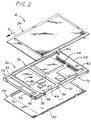
- Figure 1 illustrates a data card 10 of the present invention, which is adapted to be inserted into a slot 12 of an electronic device 14.
- the particular device shown being a thin lap top computer.
- the data card includes a housing 20 comprising a moulded plastic frame 22 and top and bottom covers 24, 26.
- the frame 22 has a top and bottom 32, 30, first and second opposite sides 34,36, and forward and rearward ends 40,42.
- a circuit board assembly 44 is mounted on the frame 22, the assembly including a circuit board 46 and a plurality of electronic components including an integrated circuit component 48 mounted on the circuit board.
- a connector 50 mounted on the forward end of the frame is connected to multiple tracks on the board, of which at least some extend to the electronic components mounted on the board.
- the data card 10 When the data card 10 is moved in a forward direction F into an electronic device, contacts of the connector 50 engage corresponding contacts on the electronic device.
- the integrated circuit components, such as 48 store data.
- the particular data card shown includes a rear connector 52 which can receive a miniature plug (not shown) to enable transmission of data between the card and an outside source (e.g. a modem), the connector having multiple contacts 54 engaged with multiple tracks on the circuit board.
- EMI electromagnetic interference
- the top and bottom covers 24, 26 are formed of electrically conductive material, such as stainless steel, to provide good EMI shielding.
- prior data cards have not provided good shielding along the perimeter of the card, that is, the outside of the card between the top and bottom covers.
- the moulded frame 22 is generally of moulded material of low electrical conductivity (at least about two orders of magnitude less than that of copper, and generally at least four orders of magnitude less).
- each rail such 70 is formed from sheet metal, as by forming it of 0.01016 cms thick copper alloy which is gold plated.
- Each rail has a side portion 74 that extends along a corresponding side 34 of the frame 22, and an end portion 76 which extends 90° from the side portion to extend along part of the rearward end 42 of the frame. It would be feasible to use a single rail which extends around both the opposite sides 34,36 and the rear end 42.
- each rail such as 70, has a height slightly more than the height of the frame 22 and a length more than half the length of the frame (between its ends 40, 42) so each side rail covers most of the peripheral area at each side 34,36 of the data card.
- each rail covers about 80% of the area of each side.
- the end portions 76 of the two rails cover about one third of the rear peripheral portion of the card.
- the data card has an imaginary vertical axis 84 that is equally spaced from its opposite sides and from its opposite ends, and has an imaginary longitudinal centerplane 86 lying halfway between the opposite sides 34,36.
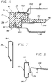
- each frame side such as 34 has top and bottom ridges 90,92.
- the rail 70 has top and bottom edge portions 94,96 that are each bent in a U shape to extend around each ridge, and thereby securely hold the rail to the frame side.
- the frame has a support wall 100 that forms a support surface 102 that supports the circuit board 46. There is substantial space between the top face 104 of the circuit board and the top cover 24, and between the bottom face 106 of the circuit aboard and the bottom cover 26. Electronic components on the circuit board can lie on and project from the top face and/or bottom face of the circuit board, and the space accommodates such projecting components.
- the frame also forms a sideward locating wall 108 which closely surrounds the circuit board 46.
- the rail 70 has a pair of tabs 110,112 which are designed to project down through a pair of through holes 114,116 in the frame side or side portion 34.
- Each tab is bent into a narrow U curve at 120, to leave a tab free end 122 extending along the bottom of the support wall 100.
- the free end 122 extends inwardly (toward the longitudinal centerplane 86 and at least partially toward the axis 84).
- the support wall has a recess 124 for accommodating the free ends of each tab, to enable the circuit board to lie securely against the support surface 102 and still allow the free end 122 of the tab to pass to a position to engage the circuit board 46.
- the ground conductor 60 of the circuit board includes a peripheral portion 130 that extends on the top and bottom faces 104,106 at the peripheral portion 134 of the board 136 of the circuit board.
- the free end 122 of the tab engages the peripheral portion 130 of the ground conductor of the circuit board, to thereby connect the circuit board ground conductor to the rail 70.
- the tab free end 122 will be soldered to the ground conductor as indicated at 138.
- the circuit board can be securely held to the frame as by adhesive.
- the locating wall 108 at the frame side has a slot 140 at the location of each tab.
- the slot facilitates forming of the tab 110 after it is projected downwardly through the hole 114 in the frame. After such downward projection, the tab is deformed, as shown.
- the U curve 120 in the tab is useful to receive a projection 142 formed along the edge of the top cover 24. This serves to ground the top cover 24 as well as helping to hold the cover in place. It may be noted that the cover also can be held to the Frame by adhesive, and also can be grounded by a grounding contact comparable to contact 54A shown in Figure 2.
- the other rail 72 is attached to the frame in a similar manner, except that its tabs, such as 150, are differently bent as shown in Figure 6.
- the tab 150 engages the peripheral portion 130 of the circuit board ground conductor and receives a bottom cover projection 152.
- the tabs can serve not only to ground the rail and the cover, but also to prevent shifting of the rail. Where the top and bottom covers are readily removable, the U loops of the tabs provide a means to help ground the tabs and help hold them in position.
- the invention provides means for providing EMI (electromagnetic interference) protection along the periphery of a data card, in a low cost construction that adds minimally to the width and length of the card.
- EMI electromagnetic interference
- the rail portions are electrically connected to the ground conductor of the circuit board mounted in the frame.
- two rails are used, each of which has a side portion covering most of the area at a corresponding side of the card frame and has a 90° bent end portion covering a portion of the rear end of the frame.
- the frame can be moulded with top and bottom vertically extending ridges, and the rail can be formed with top and bottom edge portions that extend in substantially a U bend around each ridge.
- the rail can be provided with at least one tab extending from one of the edge portions, with the tab extending through a through hole formed in the frame immediately inside the ridges. After the tab is projected downwardly through a hole, it is bent so a free end of the tab lies against a support wall that supports the circuit board assembly, and preferably lies in a recess in the support wall.
Description
Claims (9)
- A data card which includes a housing (20) having a moulded plastic frame (22) with a top (32) and a bottom (30), opposite side portions (34,36), and forward and rearward ends (40,42), the housing also having Electromagnetic interference shielding comprising sheet metal top and bottom covers (24, 26) lying respectively on the top (32) and bottom (30) of the frame (22), the card also including a circuit board assembly (44) which lies in the housing (20) and which includes a board (46) having a ground conductor (60) and at least one circuit component (48) mounted on the board, characterised in that the Electromagnetic interference shielding includes sheet metal rail portions (70, 72) extending along the outer side of the side portions (34, 36) of the frame (22), the rail portions (70, 72) extending along more than half the height and along more than half the length of the frame side portions (34, 36) to cover most of the area of the side portions, and the rail portions (70, 72) being electrically connected to the covers (24, 26) and to the board ground conductor (60).
- A data card as claimed in claim 1, characterised in that the frame sides (34,36) have a pair of ridges (90, 92) including a ridge (90) at their top and a ridge (92) at their bottom, and the rail portions (70, 72) each have top and bottom edge portions (94, 96) that are each bent in a U shape to extend around a different one of the ridges.
- A data card as claimed in claim 1 or 2, characterised in that the shielding includes an integral laterally extending tab (110) lying adjacent to one of the side portions (34, 36) the tab having a free end (122) engaging the ground conductor (60).
- A data card as claimed in claim 1 or claim 2, characterised in that the board (46) has top and bottom opposite faces (104, 106) and has a peripheral portion (134), and the ground conductor (60) has a portion lying on at least one board face at the peripheral portion, in that the frame (22) has a support wall (100) for supporting the top face (104) of the board peripheral portion (134), and the frame has a sideward locating wall (108) extending down from the support wall and surrounding the board and in that the rail portions (70, 72) have top and bottom rail edge portions (94, 96) and one of the rail edge portions (94) includes a projecting tab (110) that extends to a location between the support wall (100) and the board peripheral portion (134) and which engages the ground conductor thereat.
- A data card as claimed in claim 4, characterised in that the frame locating wall (108) has a slot (140) extending to slightly above the bottom of the support wall (100), and the support wall has a recess (124) aligned with the slot and in that the tab extends through the slot and lies in the recess and engages a ground conductor portion that lies against the support wail.
- A data card as claimed in claim 5, characterised in that the one of the fame side portions (34) has a through hole (114) extending between its top and bottom with at least part of the hole lying inward of ridges (90, 92) provided one at the top and the other at the bottom in the side portions (34, 36) and in that the rail has upper and lower edge portions (94, 96), the tab (110) extends from the upper edge portion (94) and downwardly into the hole (114), and the tab is bent to extend through the slot (140) into the recess (124).
- A data card as claimed in any preceding claim, characterised in that the rail portions (70, 72) have a 90° bend forming an end portion (76) that extends along part of one of the ends of the frame.
- A data card as claimed in claim 1, characterised in that the rail portions (70, 72) extend between the top and bottom covers (24, 26) and extend continuously substantially the entire length of the side portions (34, 36) of the frame (22).
- A data card as claimed in claims 1 or 8, characterised in that front and rear connectors (50, 52) are located at the forward and rearward ends (40, 42) of the frame (22), with the rear connector (42) being spaced from the side portions (34, 36) of the frame (22) to provide frame end areas, and the electromagnetic interference shielding has end portions (76) extending over the frame end areas.
Applications Claiming Priority (2)
| Application Number | Priority Date | Filing Date | Title |
|---|---|---|---|
| US07/906,179 US5333100A (en) | 1992-06-29 | 1992-06-29 | Data card perimeter shield |
| US906179 | 1992-06-29 |
Publications (2)
| Publication Number | Publication Date |
|---|---|
| EP0578888A1 EP0578888A1 (en) | 1994-01-19 |
| EP0578888B1 true EP0578888B1 (en) | 1998-03-04 |
Family
ID=25422055
Family Applications (1)
| Application Number | Title | Priority Date | Filing Date |
|---|---|---|---|
| EP92309982A Expired - Lifetime EP0578888B1 (en) | 1992-06-29 | 1992-10-30 | Data card perimeter shield |
Country Status (4)
| Country | Link |
|---|---|
| US (2) | US5333100A (en) |
| EP (1) | EP0578888B1 (en) |
| JP (1) | JPH0827827B2 (en) |
| DE (1) | DE69224633T2 (en) |
Families Citing this family (66)
| Publication number | Priority date | Publication date | Assignee | Title |
|---|---|---|---|---|
| DE4223322C1 (en) * | 1992-07-16 | 1993-07-29 | Schroff Gmbh, 7541 Straubenhardt, De | |
| US5339222A (en) * | 1993-04-06 | 1994-08-16 | The Whitaker Corporation | Shielded printed circuit card holder |
| US5506373A (en) * | 1993-07-09 | 1996-04-09 | Magnavox Electronic Systems Company | Electronic module enclosure |
| US5397857A (en) * | 1993-07-15 | 1995-03-14 | Dual Systems | PCMCIA standard memory card frame |
| USD379350S (en) * | 1993-08-10 | 1997-05-20 | International Business Machines Corporation | Expanded jacketted circuit card |
| US5386340A (en) * | 1993-08-13 | 1995-01-31 | Kurz; Arthur A. | Enclosure for personal computer card GPT |
| JP2581343Y2 (en) * | 1993-09-10 | 1998-09-21 | 本多通信工業株式会社 | IC card |
| US6295031B1 (en) | 1993-12-23 | 2001-09-25 | Symbol Technologies, Inc. | Memory card assembly having an integral antenna |
| US5519577A (en) * | 1993-12-23 | 1996-05-21 | Symbol Technologies, Inc. | Spread spectrum radio incorporated in a PCMCIA Type II card holder |
| US5502620A (en) * | 1994-03-11 | 1996-03-26 | Molex Incorporated | Grounded IC card |
| US5490043A (en) * | 1994-04-15 | 1996-02-06 | Hon Hai Precision Ind. Co., Ltd. | Grounding clip structure of I/O card |
| US5537294A (en) * | 1994-06-01 | 1996-07-16 | The Whitaker Corporation | Printed circuit card having a contact clip for grounding a printed circuit board found therein |
| US5497297A (en) * | 1994-06-28 | 1996-03-05 | Intel Corporation | Frame and cover structure for integrated circuit cards |
| US5600539A (en) * | 1994-10-11 | 1997-02-04 | At&T Global Information Solutions Company | Secure interface card extractor/ejector mechanism |
| US5499162A (en) * | 1994-11-08 | 1996-03-12 | International Business Machines Corp. | Universal frame for data card |
| US5539417A (en) * | 1994-11-16 | 1996-07-23 | Kelly Communications Group, Inc. | Antenna clip assembly and antenna control circuit for cellular phone |
| EP0717472A3 (en) * | 1994-12-13 | 1999-03-31 | Molex Incorporated | Grounding clip for IC-cards |
| US5602581A (en) * | 1994-12-22 | 1997-02-11 | Sony Corporation | Television receiver control box that contains a card reader mounted directly to a motherboard |
| SE506941C2 (en) * | 1995-03-31 | 1998-03-02 | Ericsson Telefon Ab L M | PCB with interference shielding layer |
| WO1996034362A1 (en) * | 1995-04-24 | 1996-10-31 | Elco Corporation | Integrated circuit card |
| JPH08337083A (en) * | 1995-06-13 | 1996-12-24 | Mitsubishi Electric Corp | Ic card |
| JP2721329B2 (en) * | 1995-12-28 | 1998-03-04 | 山一電機株式会社 | Card-in type connector |
| JP3292803B2 (en) * | 1995-12-28 | 2002-06-17 | 山一電機株式会社 | Card-in type connector |
| US5696669A (en) * | 1996-01-11 | 1997-12-09 | Molex Incorporated | Shielding system for PC cards |
| US6091605A (en) * | 1996-04-26 | 2000-07-18 | Ramey; Samuel C. | Memory card connector and cover apparatus and method |
| US5754404A (en) * | 1996-05-14 | 1998-05-19 | Itt Cannon Gmbh | IC card rear board-connector support |
| US5749741A (en) * | 1996-07-12 | 1998-05-12 | Minnesota Mining And Manufacturing Company | Electrical connector with ground clip |
| US5838542A (en) * | 1996-09-30 | 1998-11-17 | Intel Corporation | Processor card assembly including a heat sink attachment plate and an EMI/ESD shielding cage |
| US6046905A (en) * | 1996-09-30 | 2000-04-04 | Intel Corporation | Dual spring clip attachment mechanism for controlled pressure interface thermal solution on processor cartridges |
| US5991165A (en) * | 1996-12-24 | 1999-11-23 | Ericsson Inc. | Board to board RF shield with integrated connector/connector holder and method |
| US5920460A (en) * | 1997-01-11 | 1999-07-06 | Methode Electronics, Inc. | PC card receptacle with integral ground clips |
| US5833473A (en) * | 1997-03-12 | 1998-11-10 | Itt Manufacturing Enterprises, Inc. | Cardbus Bridge |
| DE19710513C2 (en) * | 1997-03-13 | 1999-10-14 | Itt Mfg Enterprises Inc | Plug-in card for electronic devices |
| EP0919950B1 (en) * | 1997-06-23 | 2007-04-04 | Rohm Co., Ltd. | Module for ic card, ic card, and method for manufacturing module for ic card |
| FI105386B (en) * | 1997-09-23 | 2000-07-31 | Nokia Mobile Phones Ltd | Cover structure for a wireless telecommunications apparatus and method of manufacture as well as wireless telecommunications apparatus |
| JPH11149539A (en) * | 1997-11-17 | 1999-06-02 | Mitsubishi Electric Corp | Ic card |
| US6122178A (en) * | 1997-11-25 | 2000-09-19 | Raytheon Company | Electronics package having electromagnetic interference shielding |
| US6433825B1 (en) * | 1997-12-18 | 2002-08-13 | Eastman Kodak Company | EMI-protected eject interface for an electronic device |
| US6515871B1 (en) | 1998-02-17 | 2003-02-04 | Intel Corporation | Protection shield for an electronic cartridge |
| US5934916A (en) * | 1998-02-24 | 1999-08-10 | Illinois Tool Works Inc. | Printed circuit board mounting rail member and ground clip assembly |
| JP3192402B2 (en) * | 1998-04-14 | 2001-07-30 | 日本圧着端子製造株式会社 | PC card frame kit, PC card, and method for manufacturing PC card |
| US6449163B1 (en) | 1998-06-08 | 2002-09-10 | Intel Corporation | Inboard retention system for processor enclosure assemblies with substrate alignment |
| US6585534B2 (en) | 1998-08-20 | 2003-07-01 | Intel Corporation | Retention mechanism for an electrical assembly |
| US6088231A (en) * | 1999-03-03 | 2000-07-11 | Methode Electronics, Inc. | RF and EMI shield |
| US6313400B1 (en) | 1999-07-13 | 2001-11-06 | Itt Manufacturing Enterprises, Inc. | Data card easily assembled housing |
| US6269537B1 (en) | 1999-07-28 | 2001-08-07 | Methode Electronics, Inc. | Method of assembling a peripheral device printed circuit board package |
| US6288344B1 (en) * | 1999-08-20 | 2001-09-11 | Cardiac Pacemakers, Inc. | Integrated EMI shield utilizing a hybrid edge |
| TW507476B (en) * | 1999-11-09 | 2002-10-21 | Gul Technologies Singapore Ltd | Printed circuit boards with in-board shielded circuitry and method of producing the same |
| US6948948B2 (en) * | 2002-07-30 | 2005-09-27 | D&C Technology Co., Ltd. | PC cartridge having enhanced front connecting structure |
| JP2004341895A (en) * | 2003-05-16 | 2004-12-02 | Sony Corp | Ic card |
| US6780056B1 (en) | 2003-07-31 | 2004-08-24 | Intercon Systems, Inc. | EMI-shielded interposer assembly |
| US7186924B2 (en) * | 2003-10-21 | 2007-03-06 | International Business Machines Corporation | Dielectric structure for printed circuit board traces |
| US20050127189A1 (en) * | 2003-12-10 | 2005-06-16 | Huang-Wei Hung | Fixture for a flash memory card |
| US7554812B2 (en) * | 2005-10-11 | 2009-06-30 | Apple Inc. | Structural support for portable electronic devices |
| US7623357B2 (en) * | 2005-11-02 | 2009-11-24 | Symbol Technologies, Inc. | Card holder arrangement for circuit assembly |
| US7518880B1 (en) * | 2006-02-08 | 2009-04-14 | Bi-Link | Shielding arrangement for electronic device |
| US7489515B2 (en) * | 2006-10-31 | 2009-02-10 | Broadtek Technology Co., Ltd. | Expansion card |
| KR101266874B1 (en) * | 2008-05-20 | 2013-05-23 | 삼성전자주식회사 | Image projecting apparatus |
| TWI355220B (en) | 2008-07-14 | 2011-12-21 | Unimicron Technology Corp | Circuit board structure |
| JP2010192759A (en) * | 2009-02-19 | 2010-09-02 | Sanyo Electric Co Ltd | Electromagnetic shield structure of electronic apparatus housing |
| US20100257732A1 (en) * | 2009-04-14 | 2010-10-14 | Ziberna Frank J | Shielding Arrangement for Electronic Device |
| US20130082365A1 (en) | 2011-10-03 | 2013-04-04 | International Business Machines Corporation | Interposer for ESD, EMI, and EMC |
| US9504175B2 (en) * | 2012-12-12 | 2016-11-22 | Fourte Internatinal, Ltd. | Solid-state drive housing, a solid-state disk using the same and an assembling process thereof |
| US20160192544A1 (en) * | 2014-12-26 | 2016-06-30 | Intel Corporation | Integrated thermal emi structure for electronic devices |
| CN106817887B (en) * | 2015-11-30 | 2020-08-18 | 深圳富泰宏精密工业有限公司 | Shielding case, shielding case assembly and electronic device applying shielding case assembly |
| USD848431S1 (en) * | 2016-01-19 | 2019-05-14 | Sony Corporation | Memory card |
Family Cites Families (30)
| Publication number | Priority date | Publication date | Assignee | Title |
|---|---|---|---|---|
| US3200261A (en) * | 1961-11-21 | 1965-08-10 | Gen Telephone & Elect | Blocking oscillator |
| BE634646A (en) * | 1962-07-20 | |||
| US3372310A (en) * | 1965-04-30 | 1968-03-05 | Radiation Inc | Universal modular packages for integrated circuits |
| US4146291A (en) * | 1977-08-03 | 1979-03-27 | Msi Data Corporation | Antistatic electrical connector housing |
| US4386388A (en) * | 1981-09-04 | 1983-05-31 | Northern Telecom Limited | Printed circuit board assembly |
| CA1204213A (en) * | 1982-09-09 | 1986-05-06 | Masahiro Takeda | Memory card having static electricity protection |
| US4780791A (en) * | 1986-04-08 | 1988-10-25 | Fujisoku Electric Co., Ltd. | Card-shaped memory having an IC module |
| US4872091A (en) * | 1986-07-21 | 1989-10-03 | Ricoh Company, Ltd. | Memory cartridge |
| JPS63242691A (en) * | 1987-03-31 | 1988-10-07 | 三菱電機株式会社 | Semiconductor-device card |
| JP2539838B2 (en) * | 1987-07-14 | 1996-10-02 | 三菱電機株式会社 | IC card device |
| JPS6458594A (en) * | 1987-08-31 | 1989-03-06 | Fanuc Ltd | Ic card |
| US4821146A (en) * | 1987-11-17 | 1989-04-11 | International Business Machines Corporation | Plugable interposer and printed circuit card carrier |
| KR930009394B1 (en) * | 1988-02-12 | 1993-10-02 | 세이꼬 엡슨 가부시끼가이샤 | Contstruction for removing electronic charges in connectors |
| JPH0278372U (en) * | 1988-12-06 | 1990-06-15 | ||
| US5107767A (en) * | 1989-06-26 | 1992-04-28 | Olin Corporation | Inflatable bladder submunition dispensing system |
| JPH07121635B2 (en) * | 1989-09-09 | 1995-12-25 | 三菱電機株式会社 | IC card |
| US5107404A (en) * | 1989-09-14 | 1992-04-21 | Astec International Ltd. | Circuit board assembly for a cellular telephone system or the like |
| EP0439122A3 (en) * | 1990-01-25 | 1992-09-09 | Tokyo Electric Co., Ltd. | Electric circuit apparatus |
| DE4036081C2 (en) * | 1990-04-26 | 1994-10-06 | Mitsubishi Electric Corp | Semiconductor memory plug-in module |
| US5053613A (en) * | 1990-05-29 | 1991-10-01 | Mitsubishi Denki Kabushiki Kaisha | IC card |
| JPH04107191A (en) * | 1990-08-28 | 1992-04-08 | Fujitsu Ltd | Ic card |
| JPH04153096A (en) * | 1990-10-18 | 1992-05-26 | Mitsubishi Electric Corp | Portable memory device |
| EP0682322B1 (en) * | 1991-09-09 | 2001-09-26 | Itt Manufacturing Enterprises, Inc. | An IC card |
| US5398154A (en) * | 1991-09-11 | 1995-03-14 | Itt Corporation | Card grounding apparatus |
| US5207586A (en) * | 1991-10-24 | 1993-05-04 | Intel Corporation | Integral connector system for credit card size I/O card external connector |
| US5414253A (en) * | 1991-12-03 | 1995-05-09 | Texas Instruments Incorporated | Integrated circuit card |
| CA2057518C (en) * | 1991-12-09 | 1996-11-19 | Albert John Kerklaan | Jacketted circuit card |
| US5242310A (en) * | 1992-06-19 | 1993-09-07 | Data Trek Corporation | PC I/O card |
| US5299940A (en) * | 1992-07-14 | 1994-04-05 | Mitsubishi Denki Kabushiki Kaisha | IC card |
| US5333360A (en) * | 1992-10-09 | 1994-08-02 | Hans Oetiker Ag Mashinen- Und Apprate-Fabrik | Expandable clamp structure of the earless type |
-
1992
- 1992-06-29 US US07/906,179 patent/US5333100A/en not_active Expired - Fee Related
- 1992-10-30 EP EP92309982A patent/EP0578888B1/en not_active Expired - Lifetime
- 1992-10-30 DE DE69224633T patent/DE69224633T2/en not_active Expired - Lifetime
-
1993
- 1993-06-29 JP JP5159308A patent/JPH0827827B2/en not_active Expired - Lifetime
-
1995
- 1995-04-17 US US08/422,811 patent/US5572408A/en not_active Expired - Lifetime
Also Published As
| Publication number | Publication date |
|---|---|
| DE69224633T2 (en) | 1998-10-22 |
| JPH0827827B2 (en) | 1996-03-21 |
| DE69224633D1 (en) | 1998-04-09 |
| JPH0668319A (en) | 1994-03-11 |
| US5333100A (en) | 1994-07-26 |
| EP0578888A1 (en) | 1994-01-19 |
| US5572408A (en) | 1996-11-05 |
Similar Documents
| Publication | Publication Date | Title |
|---|---|---|
| EP0578888B1 (en) | Data card perimeter shield | |
| US5319516A (en) | Electrostatically protected IC card | |
| EP0532166B1 (en) | Memory card grounding apparatus | |
| EP0971443B1 (en) | Electrical connector system for shielded flat flexible circuitry | |
| US6682368B2 (en) | Electrical connector assembly utilizing multiple ground planes | |
| US5477421A (en) | Shielded IC card | |
| EP0628220B1 (en) | IC card grounding system | |
| US5586893A (en) | IC card connector shield grounding | |
| US6800805B2 (en) | Noise suppressing structure for shielded cable | |
| WO1994013038A1 (en) | Ic card and cable harness | |
| US6091605A (en) | Memory card connector and cover apparatus and method | |
| US5807137A (en) | Shielded electrical receptacle connector assembly | |
| US5984727A (en) | Mini electrical connector | |
| US5667407A (en) | Shielded cable plug | |
| EP0801823B1 (en) | Shielded memory card connector | |
| JP3262758B2 (en) | Flanged connector | |
| US6626689B1 (en) | Electrical card connector | |
| US6010365A (en) | Electrical connector with improved grounding protection | |
| CA2174130C (en) | Ic card with board positioning means | |
| US6736656B1 (en) | Electrical card connector | |
| US6722921B1 (en) | Electrical card connector | |
| US11495907B2 (en) | Receptacle connector including electromagneiic compatibility (EMC) shield | |
| JPH04216697A (en) | Circuit package and shelf mounting the same |
Legal Events
| Date | Code | Title | Description |
|---|---|---|---|
| PUAI | Public reference made under article 153(3) epc to a published international application that has entered the european phase |
Free format text: ORIGINAL CODE: 0009012 |
|
| 17P | Request for examination filed |
Effective date: 19921105 |
|
| AK | Designated contracting states |
Kind code of ref document: A1 Designated state(s): DE FR GB IT |
|
| 17Q | First examination report despatched |
Effective date: 19960509 |
|
| GRAG | Despatch of communication of intention to grant |
Free format text: ORIGINAL CODE: EPIDOS AGRA |
|
| GRAG | Despatch of communication of intention to grant |
Free format text: ORIGINAL CODE: EPIDOS AGRA |
|
| GRAG | Despatch of communication of intention to grant |
Free format text: ORIGINAL CODE: EPIDOS AGRA |
|
| GRAH | Despatch of communication of intention to grant a patent |
Free format text: ORIGINAL CODE: EPIDOS IGRA |
|
| GRAG | Despatch of communication of intention to grant |
Free format text: ORIGINAL CODE: EPIDOS AGRA |
|
| GRAH | Despatch of communication of intention to grant a patent |
Free format text: ORIGINAL CODE: EPIDOS IGRA |
|
| GRAA | (expected) grant |
Free format text: ORIGINAL CODE: 0009210 |
|
| RAP1 | Party data changed (applicant data changed or rights of an application transferred) |
Owner name: ITT MANUFACTURING ENTERPRISES, INC. |
|
| AK | Designated contracting states |
Kind code of ref document: B1 Designated state(s): DE FR GB IT |
|
| ITF | It: translation for a ep patent filed |
Owner name: BUGNION S.P.A. |
|
| REF | Corresponds to: |
Ref document number: 69224633 Country of ref document: DE Date of ref document: 19980409 |
|
| ET | Fr: translation filed | ||
| PLBE | No opposition filed within time limit |
Free format text: ORIGINAL CODE: 0009261 |
|
| STAA | Information on the status of an ep patent application or granted ep patent |
Free format text: STATUS: NO OPPOSITION FILED WITHIN TIME LIMIT |
|
| 26N | No opposition filed | ||
| REG | Reference to a national code |
Ref country code: GB Ref legal event code: IF02 |
|
| PGFP | Annual fee paid to national office [announced via postgrant information from national office to epo] |
Ref country code: DE Payment date: 20101027 Year of fee payment: 19 |
|
| PGFP | Annual fee paid to national office [announced via postgrant information from national office to epo] |
Ref country code: IT Payment date: 20101028 Year of fee payment: 19 Ref country code: GB Payment date: 20101025 Year of fee payment: 19 |
|
| PGFP | Annual fee paid to national office [announced via postgrant information from national office to epo] |
Ref country code: FR Payment date: 20111028 Year of fee payment: 20 |
|
| REG | Reference to a national code |
Ref country code: DE Ref legal event code: R071 Ref document number: 69224633 Country of ref document: DE |
|
| REG | Reference to a national code |
Ref country code: DE Ref legal event code: R071 Ref document number: 69224633 Country of ref document: DE |
|
| REG | Reference to a national code |
Ref country code: GB Ref legal event code: PE20 Expiry date: 20121029 |
|
| PG25 | Lapsed in a contracting state [announced via postgrant information from national office to epo] |
Ref country code: GB Free format text: LAPSE BECAUSE OF EXPIRATION OF PROTECTION Effective date: 20121029 |