EP0592851B1 - System for applying low energy emission therapy - Google Patents
System for applying low energy emission therapy Download PDFInfo
- Publication number
- EP0592851B1 EP0592851B1 EP93115439A EP93115439A EP0592851B1 EP 0592851 B1 EP0592851 B1 EP 0592851B1 EP 93115439 A EP93115439 A EP 93115439A EP 93115439 A EP93115439 A EP 93115439A EP 0592851 B1 EP0592851 B1 EP 0592851B1
- Authority
- EP
- European Patent Office
- Prior art keywords
- storage device
- modulation signal
- patient
- control information
- modulation
- Prior art date
- Legal status (The legal status is an assumption and is not a legal conclusion. Google has not performed a legal analysis and makes no representation as to the accuracy of the status listed.)
- Expired - Lifetime
Links
Images


Classifications
-
- A—HUMAN NECESSITIES
- A61—MEDICAL OR VETERINARY SCIENCE; HYGIENE
- A61N—ELECTROTHERAPY; MAGNETOTHERAPY; RADIATION THERAPY; ULTRASOUND THERAPY
- A61N5/00—Radiation therapy
- A61N5/06—Radiation therapy using light
- A61N5/0613—Apparatus adapted for a specific treatment
- A61N5/0618—Psychological treatment
-
- A—HUMAN NECESSITIES
- A61—MEDICAL OR VETERINARY SCIENCE; HYGIENE
- A61N—ELECTROTHERAPY; MAGNETOTHERAPY; RADIATION THERAPY; ULTRASOUND THERAPY
- A61N1/00—Electrotherapy; Circuits therefor
- A61N1/02—Details
- A61N1/04—Electrodes
- A61N1/05—Electrodes for implantation or insertion into the body, e.g. heart electrode
- A61N1/0526—Head electrodes
- A61N1/0548—Oral electrodes
-
- A—HUMAN NECESSITIES
- A61—MEDICAL OR VETERINARY SCIENCE; HYGIENE
- A61N—ELECTROTHERAPY; MAGNETOTHERAPY; RADIATION THERAPY; ULTRASOUND THERAPY
- A61N1/00—Electrotherapy; Circuits therefor
- A61N1/40—Applying electric fields by inductive or capacitive coupling ; Applying radio-frequency signals
-
- A—HUMAN NECESSITIES
- A61—MEDICAL OR VETERINARY SCIENCE; HYGIENE
- A61N—ELECTROTHERAPY; MAGNETOTHERAPY; RADIATION THERAPY; ULTRASOUND THERAPY
- A61N5/00—Radiation therapy
Definitions
- the invention relates to systems for applying low energy emission therapy for the treatment of central nervous system disorders.
- the apparatus is intended for therapy or treatment of patients and the low energy emissions applied to the patient are akin to pharmaceutical medication.
- the marketing organization of a pharmaceutical industry should thus be placed in a position to market the therapy in a fashion not widely different from the fashion in which pharmaceutical products are marketed, e.g., through pharmacists, with or without a doctor's prescription.
- insomnia has lagged behind other medical research programs.
- Current treatment methods for insomnia consist either of hypnotics, behavioral therapies (e.g. biofeedback), or of the use of drug agents, specifically benzodiazepines or imidazopyridines.
- Tolerance, dependence, memory loss, and lack of efficacy in long-term treatment are among the most common drawbacks of these classes of currently available hypnotics.
- the present invention has rendered feasible an entirely new approach to treatment of a patient described in our said earlier patents while avoiding the above-noted drawbacks.
- the present invention contemplates provision of an application storage device for use in a system for applying low energy emission therapy to a patient for the treatment of central nervous system disorders. Additionally, the invention contemplates provision of a system for applying a modulated low energy electromagnetic emission to a patient via a probe.
- the application storage device of the invention comprises control information storage media selected from the group consisting of magnetic storage media, semiconductor memory storage media, mechanical storage media and optical storage media, the application storage device embodying control information for controlling an output of electromagnetic energy from the system and being connectable via an interface to such system, which system comprises program-controllable means to provide a program-controlled output of electromagnetic energy and which system further comprises a probe to apply such output of electromagnetic energy to the patient, characterised in that the application storage device embodies modulation signal control information including control information to control a programmable modulation signal generator with a plurality of modulation signals for modulating an amplitude of a high frequency low energy carrier signal generated by a controllable generator of the system to produce a modulated carrier signal modulated by a plurality of modulation signals.
- control information may further include modulation frequency control information, the system then comprising program-controllable modulation frequency generator means for generating modulation frequency controlled low energy electromagnetic signals.
- control information may comprise modulated low energy electromagnetic emission duration control information, the system then comprising programmable modulated low energy electromagnetic emission duration generator means for generating duration controlled modulated low energy electromagnetic carrier signals.
- the duration control information may comprise modulated carrier signal interruption information.
- the control information comprised in the application storage device of the invention may further comprise emission application limit information and may include patient treatment compliance information as well as power level control information.
- a microprocessor may be incorporated into the application storage device, the interface of the system then existing between the combination of the microprocessor and the application storage device and the rest of the system.
- the system of the invention comprises a controllable electromagnetic energy and amplitude modulator generator circuit for generating a high frequency low energy carrier signal, and for modulating an amplitude of the carrier signal by a modulation signal to generate a modulated carrier signal, a data processor, connected to said generator circuit, for controlling said generator circuit to produce said modulated carrier signal, and a probe for applying said modulated carrier signal to a patient, characterised in that the system is provided for use in conjunction with an application storage device as described above by including: an interface for the application storage device, connected to said data processor and adapted for connection to the application storage device, for receiving control information, including modulation signal control information, from the application storage device, and for transferring said control information to said data processor; and a programmable modulation signal generator adapted to generate a plurality of modulation signals in response to the modulation control information embodied in the application storage device to produce a modulated carrier signal modulated by a plurality of modulation signals.
- the controllable electromagnetic energy generator circuit may comprise a high frequency low energy carrier signal generator circuit; a modulation signal generator circuit; and an AM modulator and power generator connected to said carrier signal generator circuit and said modulation signal generator circuit, for modulating said hich frequency low energy carrier signal with said modulation signal to produce said modulated carrier signal.
- the modulation signal circuit in turn may comprise an addressable modulation signal storage device; an address generator, connected to and controlled by said data processor, for generating addresses for said modulation signal storage device under control of said data processor; and a digital to analog converter, connected to said modulation signal storage device, for converting a digital modulation signal output from said modulation signal storage device into an analog modulation signal.
- the modulation circuit may furthermore comprise a selective filter, connected to and controlled by said data processor, for selectively filtering said analog modulation signal to produce a filtered modulation signal; and a modulation signal buffer amplifier, connected to and controlled by said data processor, for buffering said filtered modulation signal before application to said AM modulator and power generator.
- the system of the invention may comprise an emitter circuit connected to receive said modulation signal and carrier signal and to apply said modulated carrier signal to said probe, and the emitter circuit may comprise an AM modulator for converting said modulation signal and carrier signal into a modulated carrier signal: a tuned resonant converter for amplifying the said modulated carrier signal; and a filter circuit for filtering said modulated carrier signal.
- An antenna cable may be connected intermediate said emitter circuit and said probe.
- an impedance transformer may be connected intermediate said emitter circuit and said probe to substantially match an impedance of said patient seen from said emitter with an impedance of the output of the emitter circuit.
- the impedance transformer may comprise an inductor connected intermediate said emitter circuit and said probe, and a capacitor connected intermediate ground and a point of connection between said inductor and said probe.
- the system of the invention may furthermore comprise a power sensor for detecting an amount of electromagnetic power applied to the patient and the power sensor may include a detector for detecting an amount of power applied to said patient: a detector for detecting an amount of power reflected from said patient; and means for comparing said amount of power applied to said patient with said amount of power reflected from said patient.
- the system conveniently comprises a display device, connected to and controlled by said data processor. for displaying indicia of the operation of the system.
- the probe comprised in the system may be a probe clement of electrically conductive material adapted to be applied to mucosa of the patient and the probe may be adapted to fit into a mouth of the patient.
- Figure 1 is a system for applying modulated low energy electromagnetic emission to a patient, in accordance with the present invention.
- Figure 2 is a block diagram of the circuitry of the system of Figure 1.
- FIG. 3 is a detailed schematic of the modulation signal generator of the circuit of Figure 2.
- Figure 4 is a detailed schematic of the modulation signal buffer and the carrier oscillator circuit used in the circuit of Figure 2.
- FIG. 5 is a detailed schematic of the AM modulation and power generator and output filter of the circuit of Figure 2.
- Figure 6 is a detailed schematic of the impedance transformer of the circuit of Figure 2.
- FIG. 7 is a detailed schematic of the emission sensor circuit of the circuit of Figure 2.
- Figure 8 is a detailed schematic of the output power sensor circuit used in the circuit of Figure 2.
- FIG 9 is a detailed schematic of the display module used in the circuit of Figure 2.
- FIG 10 is a detailed schematic of the power supply circuit used in the circuit of Figure 2.
- FIGs 11 a-d are flow charts of the method of operation of the system of Figure 1 and 2, in accordance with the present invention.
- Figures 12, 13, 14, 15, 16 and 17 are examples of an application storage device for use with the present invention.
- LEET Low Energy Emission Therapy
- RF radio frequency
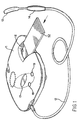
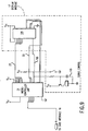
- the system includes a probe or mouthpiece 13 which is inserted into the mouth of a patient under treatment.
- Probe 13 is connected to an electromagnetic energy emitter (see also Figure 2), through coaxial cable 12 and impedance matching transformer 14.
- probe 13 is illustrated as a mouthpiece, any probe that is adapted to be applied to any mucosa may be used.
- any probe that is adapted to be applied to any mucosa may be used.
- oral, nasal, optical, urethral, anal, and/or vaginal probes may be used without departing from the scope of the invention.
- Probes situated closer to the brain for example endonasal or oral probes, are presently preferred.
- Application system 11 also includes an interface 16 which is adapted to receive an application storage device 52 such as, for example, magnetic media, semiconductor media, optical media or mechanically encoded media, which is programmed with control information used to control the operation of system 11 to apply the desired type of low energy emission therapy to the patient under treatment.
- an application storage device 52 such as, for example, magnetic media, semiconductor media, optical media or mechanically encoded media, which is programmed with control information used to control the operation of system 11 to apply the desired type of low energy emission therapy to the patient under treatment.
- application storage device 52 can be provided with a microprocessor which, when applied to interface 16, operates to control the function of system 11 to apply the desired low energy emission therapy.
- application storage device 52 can be provided with a microprocessor which is used in combination with microprocessor 21 within system 11. In such case, the microprocessor within device 52 could assist in the interfacing of storage device 52 with system 11, or could provide security checking functions.
- System 11 also includes a display 17 which can display various indications of the operation of system 11.
- system 11 includes on and off power buttons 18 and 19.
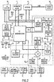
- Microprocessor 21 operates as the controller for application system 11, and is connected to control the various components of the system 11 through address bus 22, data bus 23 and I/O lines 25.
- Microprocessor 21 preferably includes internal storage for the operation code, control program, and temporary data.
- microprocessor 21 includes input/output ports and internal timers.
- Microprocessor 21 may be, for example, an 8-bit single-chip microcontroller, 8048 or 8051 available from Intel Corporation
- system clock 24 which includes a clock crystal 26 along with capacitors 27 and 28.
- System clock 24 may run at any clock frequency suitable for the particular type of microprocessor used. In accordance with one embodiment of the present invention, system clock 24 operates at a clock frequency of 8.0 MHz.
- microprocessor 21 functions to control controllable electromagnetic energy generator circuit 29 to produce a desired form of modulated low energy electromagnetic emission for application to a patient through probe 13.
- Controllable generator circuit 29 includes modulation frequency generator circuit 31 and carrier signal oscillator 32.
- Microprocessor 21 operates to activate or de-activate controllable generator circuit 29 through oscillator disable line 33, as described below in more detail.
- Controllable generator circuit 29 also includes an AM modulator and power generator 34 which operates to amplitude modulate a carrier signal produced by carrier oscillator 32 on carrier signal line 36, with a modulation signal produced by modulation signal generator circuit 31 on modulation signal line 37.
- Modulator 34 produces an amplitude modulated carrier signal on modulated carrier signal line 38, which is then applied to the filter circuit 39.
- the filter circuit 39 is connected to probe 13 via coaxial cable 12 and impedance transformer 14.
- Microprocessor 21 controls modulation signal generator circuit 31 of controllable generator circuit 29 through address bus 22, data bus 23 and I/O lines 25. In particular, microprocessor 21 selects the desired waveform stored in modulation waveform storage device 43 via I/O lines 25. Microprocessor 21 also controls waveform address generator 41 to produce on waveform address bus 42 a sequence of addresses which are applied to modulation signal storage device 43 in order to retrieve the selected modulation signal. The desired modulation signal is retrieved from modulation signal storage device 43 and applied to modulation signal bus 44 in digital form. Modulation signal bus 44 is applied to digital to analog converter (DAC) 46 which converts the digital modulation signal into analog form.
- DAC digital to analog converter
- This analog modulation signal is then applied to selective filter 47 which, under control of microprocessor 21, filters the analog modulation signal by use of a variable filter network including resistor 48 and capacitors 49 and 51 in order to smooth the wave form produced by DAC 46 on modulation signal line 20.
- the various modulation signal wave forms are stored in modulation signal storage device 43.
- storage device 43 can contain up to 8 different modulation signal wave forms.
- Wave forms that have been successfully employed include square wave forms or sinusoidal wave forms.
- Other possible modulation signal wave forms include rectified sinusoidal, triangular, and combinations of all of the above.
- each modulation signal wave form uses 256 bytes of memory and is retrieved from modulation signal storage device 43 by running through the 256 consecutive addresses.
- the frequency of the modulation signal is controlled by how fast the wave form is retrieved from modulation signal storage device 43. In accordance with the present embodiment, this is accomplished by downloading a control code from microprocessor 21 into programmable counters contained within wave form address generator 41. The output of the programmable counters then drives a ripple counter that generates the sequence of 8-bit addresses on the wave form address bus 42.
- Wave form address generator 41 may be, for example, a programmable timer/counter uPD65042C, available from NEC.
- Modulation signal storage device 43 may be, for example, a type 28C16 Electrical Erasable Programmable Read Only Memory (EEPROM) programmed with the desired wave form table.
- Digital to analog converter 46 may be, for example, a DAC port, AD557JN available from Analog Devices, and selective filter 47 may be a type 4052 multiplexer, available from National Semiconductor or Harris Semiconductor.
- application storage device 52 may be any storage device capable of storing information for later retrieval.
- application storage device 52 may be, for example, a magnetic media based storage device such as a card, tape, disk, or drum.
- application storage device 52 may be a semiconductor memory-based storage device such as an erasable programmable read only memory (EPROM), an electrical erasable programmable read only memory (EEPROM) or a non-volatile random access memory (RAM).
- EPROM erasable programmable read only memory
- EEPROM electrical erasable programmable read only memory
- RAM non-volatile random access memory
- Another alternative for application storage device 52 is a mechanical information storage device such as a punched card, cam, or the like.
- Yet another alternative for application storage device 52 is an optical storage device such as a compact disk read only memory (CD ROM).
- CD ROM compact disk read only memory
- microprocessor 21 separate from application storage device 52
- microprocessor 21 and application storage device 52 may both be incorporated into a single device, which is loaded into system 11 to control the operation of system 11 as described herein.
- interface 16 would exist between the combination of microprocessor 21 and application storage device 52 and the rest of system 11.
- Interface 16 is configured as appropriate for the particular application storage device 52 in use. Interface 16 translates the control information stored in application storage device 52 into a usable form for storage within the memory of microprocessor 21 to enable microprocessor 21 to control controllable generator circuit 29 to produce the desired modulated low energy emission.
- Interface 16 may directly read the information stored on application storage device 52, or it may read the information through use of various known communications links. For example, radio frequency, microwave, telephone or optical based communications links may be used to transfer information between interface 16 and application storage device 52.
- radio frequency, microwave, telephone or optical based communications links may be used to transfer information between interface 16 and application storage device 52.
- interface 16 is configured to connect microprocessor 21 to the rest of system 11.
- control information stored in application storage device 52 specifies various controllable parameters of the modulated low energy RF electromagnetic emission which is applied to a patient through probe 13.
- controllable parameters include, for example, the frequency and amplitude of the carrier, the amplitudes and frequencies of the modulation of the carrier, the duration of the emission, the power level of the emission, the duty cycle of the emission (i.e., the ratio of on time to off time of pulsed emissions applied during an application), the sequence of application of different modulation frequencies for a particular application, and the total number of treatments and duration of each treatment prescribed for a particular patient.
- the carrier signal and modulation signal may be selected to drive the probe 13 with an amplitude modulated signal in which the carrier signal includes spectral frequency components below 1 GHz, and preferably between 1 MHz and 900 Mhz, and in which the modulation signal comprises spectral frequency components between 0.1 Hz and 10 KHz, and preferably between 1 Hz and 1000 Hz.
- one or more modulation frequencies may be sequenced to form the modulation signal.
- an electromagnetic emission sensor 53 may be provided to detect the presence of electromagnetic emissions at the frequency of the carrier oscillator 32. Emission sensor 53 provides to microprocessor 21 an indication of whether or not electromagnetic emission at the desired frequency are present. As described below in more detail, microprocessor 21 then takes appropriate action, for example, displaying an error message on display 17, disabling controllable generator circuit 29, or the like.
- the invention also includes a power sensor 54 which detects the amount of power applied to the patient through probe 13 compared to the amount of power returned or reflected from the patient. This ratio is indicative of the proper use of the system during a therapeutic session.
- Power sensor 54 applies to microprocessor 21 through power sense line 56 an indication of the amount of power applied to patient through probe 13 relative to the amount of power reflected from the patient.
- the indication provided on power sense line 56 may be digitized and used by microprocessor 21, for example, to detect and control a level of applied power, and to record on application storage device 52 information related to the actual treatments applied. Such information may then be used by a physician or other clinician to assess patient treatment compliance and effect.
- treatment information may include, for example: the number of treatments applied for a given time period; the actual time and date of each treatment; the number of attempted treatments; the treatment compliance (i.e., whether the probe was in place or not in place during the treatment session); and the cumulative dose of a particular modulation frequency.
- the level of power applied is preferably controlled to cause the specific absorption rate (SAR) of energy absorbed by the patient to be from 1 microwatt per kilogram of tissue to 50 Watts per kilogram of tissue.
- the power level is controlled to cause an SAR of from 100 microwatts per kilogram of tissue to 10 Watts per kilogram of tissue.
- the power level is controlled to cause an SAR of from 1 milliWatt per kilogram of tissue to 100 milliwatts per kilogram of tissue.
- SARs may be in any tissue of the patient, but are preferably in the tissue of the central nervous system.
- System 11 also includes powering circuitry including battery and charger circuit 57 and battery voltage change detector 58.
- FIGS 3-10 present in more detail various components of the system of Figure 2.
- Modulation frequency generator 31 includes wave form address generator 41, modulation signal storage device 43, digital to analog converter 46 and a selective filter network 47.
- Microprocessor 21 controls extended I/O lines 45 and selects the desired wave form from wave form storage device 43. Microprocessor 21 then downloads the control information to the wave form address generator 41 which in turn generates a sequence of the wave form addresses. The sequence of addresses are then applied to the modulation signal storage device 43 through address bus 42. The desired modulation signal is then retrieved from the storage device 43 and appears on signal bus 44 in digital form. After a digital to analog conversion by the digital to analog converter 46, the modulation signal is filtered and is output onto the modulation signal line 20.
- the frequency of the modulation signal is determined by the rate at which the sequence of wave form addresses is generated.
- the type of modulation signal is selected by microprocessor 21 via extended I/O lines 45 and the filtering network is selected via I/O line 50.
- the modulation signal buffer amplifier 35 is basically a noninverting amplifier in discrete form.
- the amplifier buffers the modulation signal 20 from the selective filter 47 and provides necessary modulation signal amplitude and current drive to the AM modulator and power generator circuit 34.
- the output stage is designed in such a way that the output signal 37 achieves a rail-to-rail voltage swing.
- the output of the modulation signal buffer appears on signal line 37.
- the disclosed embodiment contemplates that the gain of modulation signal buffer amplifier 35 is substantially constant, the invention also contemplates use of a variable gain amplifier that is controlled by microprocessor 21 in order to vary the magnitude of the modulation signal on line 37, thus permitting programmable control of the level of power applied.
- the carrier oscillator 32 is constructed around carrier oscillator crystal 59.
- carrier oscillator 32 produces a Radio Frequency (RF) carrier frequency of 27 MHz.
- RF Radio Frequency
- Other embodiments of the invention contemplate RF carrier frequencies of 48 MHz, 450 MHz or 900 MHz.
- the RF carrier frequency produced by carrier oscillator 32 has spectral frequency components less than 1 GHz and preferably between 1 MHz and 900 MHz.
- carrier frequency produced by carrier oscillator 32 is variable and controllable by microprocessor 21 by use of control information stored on application storage device 52. This would be accomplished, for example, by use of high frequency oscillator, the output of which is conditioned by a controllable clock divider circuit to produce a controlled carrier frequency signal.
- Carrier oscillator 32 produces on carrier signal line 36 a carrier signal which is to be modulated by the modulation signal carried on signal line 37.
- Oscillator disable line 33 is applied to NAND gate 61, the output of which is applied to NAND gate 62. This configuration allows microprocessor 21 to disable both modulation signal buffer 35 and carrier oscillator 32 by applying an appropriate disable signal to oscillator disable line 33.
- FIG. 5 presents a detailed schematic of the AM modulator and power generator 34 and the output filter 39.
- the AM modulator is made up of two transistors 66 and 67 connected in parallel and operated in zero-crossing switching mode.
- the carrier signal 36 is applied at the bases of the transistors 66 and 67 through NAND gates 63 and 64, and the modulation signal 37 is applied to the collectors of transistors 66 and 67 through inductors 68 and 69.
- the net result is the modulated carrier that appears at the collectors of the transistors 66 and 67.
- the output power is generated by a single-ended tuned resonant converters configured by three pairs of inductors and capacitors, 70, 71 and 72.
- LC resonant circuits 70, 71 and 72 are tuned to provide the required output power and are optimized to the maximum efficiency of the converter.
- the output of the AM modulator and power generator 34 appears on signal line 38.
- This modulated signal is applied through output filter network 39 to output connector 78.
- Output filter 39 included three LC filtering stages, 73, 74 and 76.
- the first LC filtering stage, 73 is a band-pass and band-notch filter with pass band centered at 27 MHz and band notch centered at 54 MHz.
- the band-notch filter provides additional suppression to the second harmonic of the carrier.
- the second and third LC filtering stages 74 and 76 are both band pass filters which have pass band centered at 27 MHz.
- the three stage output filter serves to substantially eliminate the carrier harmonics that result from zero-crossing switching of the AM modulator circuit 34.
- the output series resistor 77 is used to adjust the output impedance of the modulator. It is found from measurement that the output impedance of the AM modulator is considerably lower than 50 ohm. The series resistor 77 adjusts the output impedance of the circuit is approximately 50 ohms.
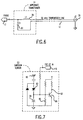
- FIG 6 presents the details of the impedance transformer 14.
- the output of the AM modulator and power generator 34 and filter stage 39 is designed to have a 50 Ohm output impedance which is chosen to match the 50 Ohm impedance of coaxial cable 12.
- Impedance transformer 14 includes inductor 79 connected between probe 13 and the middle conductor of coaxial cable 12, and a capacitor 81 connected between probe 13 and the ground conductor of coaxial cable 12.
- Impedance transformer 14 serves to match this complex impedance with the 50 Ohm impedance of coaxial cable 12 and therefore the output impedance of the AM modulator 34 and output filter 39. This promotes power transmission, and minimizes reflections.
- inductor 79 is 0.68 microHenry
- capacitor 81 is 47 picoFarads.
- FIG. 7 presents the detailed schematic of the emission sensor 53 of the present invention.
- Emission sensor 53 includes antenna 82 which is capable of detecting electromagnetic fields at the frequency of the carrier oscillator 32.
- the signal induced by antenna 82 is applied to a simple diode detector formed by diode 83, capacitor 84 and resistor 85.
- the demodulated low frequency signal is then applied to the base of a transistor 86 operating as a switch.
- the output is a low level signal line 87 which is connected to microprocessor 21.
- Emission sensor 53 is used at the beginning of a treatment session to detect whether probe 13 is emitting electromagnetic fields of the carrier frequency. If so, microprocessor 21 produces on display 17 an indication that the proper electromagnetic field is being produced.
- Emission sensor 53 is also connected to the power supply circuitry through EXT DC IN line 115 (see also, Figure 10).
- EXT DC IN line 115 which is connected to the base of transistor 86, turns transistor 86 on, thus providing an indication to microprocessor 21 that external dc power is applied.
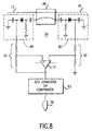
- FIG 8 presented is a schematic of the power sensor 54 used to sense the ratio of the power applied to the patient through probe 13 to the power reflected from the patient. This ratio is indicative of the efficiency of power transfer from the application system 11 to the patient, and may be used to assess patient treatment compliance. Power sensor 54 may also be used to monitor the level of power being applied to the patient.
- Power sensor 54 includes bi-directional coupler 88 which can be, for example, a model KDP-243 bi-directional coupler available from Synergy Microwave Corporation.
- Bi-directional coupler 88 operates to couple a portion of the energy emitted by application system 11 through output connected 78 and carried by coaxial cable 12 into detecting circuits 89 and 90.
- Output connector 78 is connected to a primary input of bi-directional coupler 88 and co-axial cable 12 is connected to a primary output of bi-directional coupler 88.
- Bi-directional coupler 88 includes two secondary outputs, each of which are connected to respective detecting circuits 89 and 90.
- Detecting circuit 89 functions to detect the amount of power applied to the patient, and detecting circuit 90 functions to detect the amount of power reflected from the patient.
- Detecting circuit 89 is connected through resistive divider 94 to the positive input of differential amplifier 91.
- Detecting circuit 90 is connected through resistive divider 92 to the negative input of differential amplifier 91.
- the output of differential amplifier 91 is indicative of the difference between the power transmitted to the patient by application system 11, and the power reflected from the patient, and thus is indicative of an amount of power absorbed by the patient.
- the output of differential amplifier 91 is applied to an analog to digital converter (ADC) or comparator 93, the output of which connected to microprocessor 21 through power sense line 56.
- ADC analog to digital converter
- microprocessor 21 operates to analyze the signal appearing on power sense line 56 to determine and control the amount of power applied to the patient, and to assess patient treatment compliance, and possibly to record indicia of the patient treatment compliance on application storage device 52 for later analysis and assessment by a physician or other clinician.
- FIG 9 presents a detailed schematic of the information output circuit 17.
- Microprocessor 21 controls the display module 109 of information output circuit 17 via data bus 23 and address bus 22 and controls the sound control circuit 110 by an I/O line 100.
- the display module 109 may be an intelligent LED display module PD3535, available from Siemens or a LCD graphics module available from Epson.
- the sound control circuit 110 may be a buzzer as shown in Figure 9 or it may be an advanced speech synthesizer.
- rechargeable battery 95 which may be, for example, a six volt rechargeable Ni-Cd battery, or the like.
- Battery 95 is connected through relay 99 to relay 98.
- the coil of relay 98 is powered by transistor 106 which is controlled by the output of NAND gate 102.
- NAND gates 102, 103, 104 and 105 are configured to form a resettable latch.
- the latch turns on transistor 106 which activates the coil of relay 98.
- the latch is reset thus turning transistor 106 off, and removing power from the coil of relay 98.
- Microprocessor 21 may also reset the latch by pulling low momentarily on the Auto-Off line 107. This helps to save unnecessary power consumption when the system 11 is being left in an idle state.
- Connector 96 is provided to accommodate an external ac/dc adapter (not shown) which is used to charge battery 95.
- voltage regulator 101 produces a regulated voltage which powers the coil of relay 99. This causes battery 95 to be disconnected from voltage regulator 97, and causes the output of voltage regulator 101 to be connected to the input of voltage regulator 97, thus permitting application system 11 to be powered by the external dc adapter.
- An indication of the existence of external dc voltage is applied to emission sensor 53 (Fig. 7) through EXT DC IN line 115.
- microprocessor 21 executes the battery charging control routine, stops controllable generator 29 and disables the carrier oscillator 32. It also sends a signal to the battery charging control 57 and turns on the fast charging circuits. A message is displayed on display 17 or on a separate light emitting diode indicating that the battery is being charged.
- microprocessor 21 constantly monitors the battery voltage from the -dV detector 58 via data bus 23. Once the required -dV is detected, Ni-Cd battery 95 has reached its full charge condition, microprocessor 21 switches off the fast charge circuit and automatically removes power from the system 11.
- -dV detector 58 may be configured, for example, including a MAX166 digital to analog converter available from Maxim Integrated Products, Inc.
- the battery voltage is constantly monitored by the battery voltage monitor 108. Once the battery voltage drops to a predetermined low level (the voltage level at which the output emission power drops by 3% of the calibrated value), a signal is provided to microprocessor 21 which in turn stops the emission and provides an error message on the display 17.
- Battery voltage monitor 108 may be, for example, a voltage supervisory integrated circuit available from Texas Instruments or SGS Thompson.
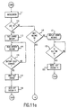
- FIGS 11 a-d presented are flow charts of the operation of the application system 11 of Figures 1 and 2, in accordance with the method of the present invention.
- the flowcharts of Figures 11 a-d are encoded in an appropriate computer program and loaded into the operating program storage portion of microprocessor 21 in order to cause microprocessor 21 to control the function of application system 11.
- microprocessor 21 starts execution of the program when switch 18 is activated.
- microprocessor 21 initializes the circuits by stopping the wave form address generator 41, disabling the carrier oscillator 32 and displaying a welcome message to the user on display module 109.
- the source of dc power is immediately checked after initialization. If an external dc power source is connected, for example an ac/dc adapter, it is assumed that system 11 should function as a Ni-Cd battery charger.
- Microprocessor 21 passes control to block 113 which switches on the fast charge mode of the battery charging control 57 and monitors the battery voltage via the -dV detector 58 in the control loop including blocks 111 and 116. Once the Ni-Cd battery 95 reaches its full-charged state as detected by -dV detector 58, microprocessor 21 switches off the fast charging current in block 117 and automatically switches off system 11 in block 118.
- decision block 112 determines that external dc source is not connected, system 11 is powered by the internal battery 95.
- the battery voltage monitor 108 monitors the battery voltage at all times and provides information to microprocessor 21 for use in decision block 119. If the battery level drops to a predetermined low level, microprocessor 21 displays an error message on the display 109 in block 121. This is to inform the user to re-charge the battery before using the system again. It also switches off system 11 automatically in block 122 if there is no user response as determined by timing loop 123.
- microprocessor 21 checks in block 124 if application storage device 52 is connected to system 11 via interface 16. If application storage device 52 is not connected, microprocessor 21 prompts for the application storage device 52 via information on display 109 in block 126. The application storage device 52 must be connected within a predetermined time limit as determined by block 127, or microprocessor 21 switches system 11 off in block 128.
- microprocessor 21 reads an identification code in block 129 and checks if application storage device 52 is genuine and valid in block 131. If not, an error message is displayed in block 132 and system 11 is switched off after a predetermined time limit.
- microprocessor 21 If a valid application storage device is connected, microprocessor 21 reads the control information in block 133 and stores the control information in the internal RAM area. Application information such as the type of treatment may be displayed on display 17 in block 134 for user re-confirmation. Microprocessor 21 then pauses and waits in block 136 for input from the user to start the application.
- Microprocessor 21 starts the application by pressing the on switch 18 again.
- Microprocessor 21 generates a test emission in block 137 by controlling the controllable generator 29 and prompts the user to check the emission with emission sensor 53 in block 138.
- Microprocessor 21 then checks the emission sensor input for the indicative signal in block 139. If the emission is not detected within a predetermined time limit as determined by block 142, microprocessor 21 displays a corresponding error message in block 143 and switches off system 11 in block 144 after a predetermined idle time as determined by block 146.
- control a passes to block 147 where microprocessor 21 executes the application software routine shown in detail in the flowchart of Figure 11d.
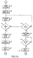
- the application software routine takes in the control information, interprets the information and controls the controllable generator 29 to generate the corresponding modulation wave form, frequency, power level, duration and duty cycle.
- microprocessor 21 starts the routine by first setting up a total treatment time counter in block 151 which keeps tracks of the timing of the actual application. It then gets and interprets the first block of modulating frequency data in block 152. Then, in block 153 the modulation wave form is selected via extended I/O lines 45 and a suitable filter network is selected via the extended I/O lines 50. Also in block 153, the gain of modulation signal buffer amplifier 35 is adjusted in accordance with the power level control information. In block 154, the modulation frequency is controlled via the wave form address generator 41. The emission is then enabled by microprocessor 21 in block 156.
- decision block 157 the battery is checked using battery voltage monitor 108 to determine whether the battery level is acceptable. If not, control passes to block 158 where an appropriate error message is displayed. Then, system 11 is shut down in block 161 after a delay time determined by decision block 159.
- control passes to block 166 where application storage device 52 is updated with user compliance information. Control then passes to block 167 where the output of power sensor 54 is read. Control then passes to block 168 where the output of power sensor 54 is assessed to determine a level of power being applied to the patient, and to assess whether or not treatment is being effectively applied. For example, if sensor 54 determines the presence of a large amount of reflected power, this condition may possibly be indicative of probe 13 not being properly connected or not being properly inserted into the mouth of a patient.
- decision block 168 determines that treatment is not being properly applied, control passes to decision block 169 which determines whether a predetermined time limit has been exceeded without detection of proper treatment. If the time limit is exceeded, control passes to block 171 where application storage device 52 is updated with information indicative of non-compliance with the treatment protocol.
- decision block 168 determines that the treatment it is being properly applied, control passes to block 172 where it is determined whether the end of the particular modulation frequency block being applied has been reached. If not, control returns to decision block 157. If, on the other hand, decision block 172 determines that the end of the modulation frequency block presently being applied has been reached, control passes to decision block 173 where it is determined whether the end of the treatment time has been reached. If so, control returns to block 148 ( Figure lic). If, on the other hand, decision block 173 determines that the end of the treatment session has not been reached, control passes to block 174 where the next frequency block is read from application storage device 52, and control returns to block 153 for the continuation of the treatment session. At the end of the application routine, control is returned and the microprocessor 21 displays an ending message in block 148 and switches system 11 off automatically in block 149.
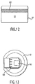
- Figures 12, 13, 14, 15, 16 and 17 present exemplary configurations for application storage device 52. It should be understood that other configurations for application storage device 52 are also possible, without departing from the scope of the present invention.
- application storage device 52 may comprise a magnetically encoded card 181 which includes a magnetically recordable portion 182 which stores the above-described control information and patient treatment compliance information.
- application storage device 52 may comprise a semiconductor memory 183 which is connected through terminals 184 to interface 16.
- Semiconductor memory 183 is used to store the above described application control information and patient treatment compliance information.
- application storage device 52 may be in the form of a smart card 186 with the semiconductor hidden behind the contacts 187.
- the semiconductor may comprise only the memory with some security control logic, or may also include a stand-alone microprocessor that assists in communicating with the host microprocessor 21 via interface 16.
- application storage device 52 may take the form of a key-shaped structure 188 including semiconductor memory 189 and microprocessor 191 which are operatively connected to electrical terminals 192.
- Figure 16 illustrates application storage device 52 in the form of a compact disk read only memory (CDROM) 193, on which control information is optically encoded.
- CDROM compact disk read only memory
- application storage device 52 may take the form of a punched card 194, in which control information is tangibly embodied in a pattern of punched holes 196.
Description
- The invention relates to systems for applying low energy emission therapy for the treatment of central nervous system disorders.
- Low energy emission therapy involving application of low energy electromagnetic emissions to a patient has been found to be an effective mode of treating a patient suffering from central nervous system (CNS) disorders such as generalized anxiety disorders, panic disorders, sleep disorders including insomnia, circadian rhythm disorders such as delayed sleep, psychiatric disorders such as depression, obsessive compulsive disorders, disorders resulting from substance abuse, sociopathy, post traumatic stress disorders or other disorders of the central nervous system. Apparatus and methods for carrying out such treatment are described in U.S. Patent Nos 4,649,935 and 4,765,322, assigned to the same assignee as the present application. Since the time of these earlier disclosures, a substantially greater understanding of the mechanisms of the treatment and how to secure best results has been gained, which has led to important developments being made to the apparatus (herein described as a system).
- Although the apparatus and methods described in the above patents have provided satisfactory results in many cases, consistency and significance of results has sometimes been lacking. Also, it was not always possible to properly control or monitor the duration of treatment or the quantities or nature of the low energy emissions being applied to the patient. Furthermore, the efficiency of transfer of the low energy emissions to the patient was limited and was affected by such factors as patient movement, outside interference and the like.
- Another limitation of the previously described apparatus is that it is not very amenable to ready marketing by marketing organizations specifically of the nature comprised in the pharmaceutical industry. The apparatus is intended for therapy or treatment of patients and the low energy emissions applied to the patient are akin to pharmaceutical medication. The marketing organization of a pharmaceutical industry should thus be placed in a position to market the therapy in a fashion not widely different from the fashion in which pharmaceutical products are marketed, e.g., through pharmacists, with or without a doctor's prescription.
- Research on treatment for insomnia has lagged behind other medical research programs. Current treatment methods for insomnia consist either of hypnotics, behavioral therapies (e.g. biofeedback), or of the use of drug agents, specifically benzodiazepines or imidazopyridines. Tolerance, dependence, memory loss, and lack of efficacy in long-term treatment are among the most common drawbacks of these classes of currently available hypnotics.
- Research throughout the past two decades has shown clearly that the brain serves not only as a communication link and thought-processing organ, but also as the source of significant chemical activity, as well as a number of bioactive compounds. Many of these neurotransmitter compounds and ions are secreted following chemical or electrical stimuli. Research has also shown that some of these neuroactive compounds are involved in the regulation of sleep and wake cycles (Koella, "The Organization and Regulation of Sleep," Experientia, 1984; 40(4): 309-408).
- During the 1970s, Adey and his group demonstrated that weak electromagnetic fields, modulated at certain well-defined low frequencies, were able to modify the release of ions (calcium) and neurotransmitters (GABA) in the brain (Kaczmarek and Adey, "The Eflux of 45Ca2+ and [3H]y-aminobutyric Acid from Cat Cerebral Cortex," Brain Research, 1973; 63:331-342; Kaczmarek and Adey, "Weak Electronic Gradients Change Ionic and Transmitter Fluxes in Cortex," Brain Research, 1974; 66:537-540; Bawin et al., "Ionic Factors in Release of 45Ca2+ From Chicken Cerebral Tissue by Electromagnetic Fields," Proceedings of the National Academy of Science, 1978; 75(12):6314-6318). In these experiments the cortex of anaesthetized cats was initially incubated with radio-labeled calcium and radio-labeled GABA. When the cortex was exposed to continuous stimulation by weak electric fields modulated at 200 Hz, the researchers found a 1.29-fold increase in Ca++ and a 1.21-fold increase in GABA release (Kaczmarek and Adey, Brain Research, 1973; 63:331-342). Interestingly, the release of GABA happened in parallel with the release of Ca++, suggesting that the two phenomena are closely linked. The findings of increased Ca++ release from brain tissue upon stimulation with modulated electromagnetic fields have been replicated (Dutta et al., "Microwave Radiation Induced Calcium Ions Effused from Human Neuroblastoma Cells in Culture," Bioelectromagnetics, 1984; 5(1):71-78; and Blackman et al., "Influence of Electromagnetic Fields on the Efflux of Calcium Ions from Brain Tissue in Vitro," Bioelectromagnetics, 1988; 9:215-227). It now has become an established fact that weak electric fields modulated at certain low frequencies are able to modulate the release of Ca++ and GABA.
- During 1983, it was discovered that weak electromagnetic fields, modulated at low frequencies and delivered by means of an antenna placed in the buccal cavity, caused changes in EEG readings in human volunteers. In agreement with the findings of Adey and Blackman, it was found that only certain well-defined low frequency modulations of a standard carrier frequency (27 MHz), emitted with a well-defined intensity, were capable of eliciting EEG changes.
- The present invention has rendered feasible an entirely new approach to treatment of a patient described in our said earlier patents while avoiding the above-noted drawbacks.
- The present invention contemplates provision of an application storage device for use in a system for applying low energy emission therapy to a patient for the treatment of central nervous system disorders. Additionally, the invention contemplates provision of a system for applying a modulated low energy electromagnetic emission to a patient via a probe.
- The application storage device of the invention comprises control information storage media selected from the group consisting of magnetic storage media, semiconductor memory storage media, mechanical storage media and optical storage media, the application storage device embodying control information for controlling an output of electromagnetic energy from the system and being connectable via an interface to such system, which system comprises program-controllable means to provide a program-controlled output of electromagnetic energy and which system further comprises a probe to apply such output of electromagnetic energy to the patient, characterised in that the application storage device embodies modulation signal control information including control information to control a programmable modulation signal generator with a plurality of modulation signals for modulating an amplitude of a high frequency low energy carrier signal generated by a controllable generator of the system to produce a modulated carrier signal modulated by a plurality of modulation signals.
- The above-mentioned control information may further include modulation frequency control information, the system then comprising program-controllable modulation frequency generator means for generating modulation frequency controlled low energy electromagnetic signals. Furthermore, the control information may comprise modulated low energy electromagnetic emission duration control information, the system then comprising programmable modulated low energy electromagnetic emission duration generator means for generating duration controlled modulated low energy electromagnetic carrier signals. The duration control information may comprise modulated carrier signal interruption information.
- The control information comprised in the application storage device of the invention may further comprise emission application limit information and may include patient treatment compliance information as well as power level control information.
- A microprocessor may be incorporated into the application storage device, the interface of the system then existing between the combination of the microprocessor and the application storage device and the rest of the system.
- The system of the invention comprises a controllable electromagnetic energy and amplitude modulator generator circuit for generating a high frequency low energy carrier signal, and for modulating an amplitude of the carrier signal by a modulation signal to generate a modulated carrier signal, a data processor, connected to said generator circuit, for controlling said generator circuit to produce said modulated carrier signal, and a probe for applying said modulated carrier signal to a patient, characterised in that the system is provided for use in conjunction with an application storage device as described above by including: an interface for the application storage device, connected to said data processor and adapted for connection to the application storage device, for receiving control information, including modulation signal control information, from the application storage device, and for transferring said control information to said data processor; and a programmable modulation signal generator adapted to generate a plurality of modulation signals in response to the modulation control information embodied in the application storage device to produce a modulated carrier signal modulated by a plurality of modulation signals.
- The controllable electromagnetic energy generator circuit may comprise a high frequency low energy carrier signal generator circuit; a modulation signal generator circuit; and an AM modulator and power generator connected to said carrier signal generator circuit and said modulation signal generator circuit, for modulating said hich frequency low energy carrier signal with said modulation signal to produce said modulated carrier signal. The modulation signal circuit in turn may comprise an addressable modulation signal storage device; an address generator, connected to and controlled by said data processor, for generating addresses for said modulation signal storage device under control of said data processor; and a digital to analog converter, connected to said modulation signal storage device, for converting a digital modulation signal output from said modulation signal storage device into an analog modulation signal. The modulation circuit may furthermore comprise a selective filter, connected to and controlled by said data processor, for selectively filtering said analog modulation signal to produce a filtered modulation signal; and a modulation signal buffer amplifier, connected to and controlled by said data processor, for buffering said filtered modulation signal before application to said AM modulator and power generator.
- The system of the invention may comprise an emitter circuit connected to receive said modulation signal and carrier signal and to apply said modulated carrier signal to said probe, and the emitter circuit may comprise an AM modulator for converting said modulation signal and carrier signal into a modulated carrier signal: a tuned resonant converter for amplifying the said modulated carrier signal; and a filter circuit for filtering said modulated carrier signal. An antenna cable may be connected intermediate said emitter circuit and said probe. Furthermore, an impedance transformer may be connected intermediate said emitter circuit and said probe to substantially match an impedance of said patient seen from said emitter with an impedance of the output of the emitter circuit. The impedance transformer may comprise an inductor connected intermediate said emitter circuit and said probe, and a capacitor connected intermediate ground and a point of connection between said inductor and said probe.
- The system of the invention may furthermore comprise a power sensor for detecting an amount of electromagnetic power applied to the patient and the power sensor may include a detector for detecting an amount of power applied to said patient: a detector for detecting an amount of power reflected from said patient; and means for comparing said amount of power applied to said patient with said amount of power reflected from said patient.
- The system conveniently comprises a display device, connected to and controlled by said data processor. for displaying indicia of the operation of the system.
- The probe comprised in the system may be a probe clement of electrically conductive material adapted to be applied to mucosa of the patient and the probe may be adapted to fit into a mouth of the patient.
- These and other features and advantages of the present invention will become apparent to those of skill in this art with reference to the appended drawings and following detailed description.
- Figure 1 is a system for applying modulated low energy electromagnetic emission to a patient, in accordance with the present invention.
- Figure 2 is a block diagram of the circuitry of the system of Figure 1.
- Figure 3 is a detailed schematic of the modulation signal generator of the circuit of Figure 2.
- Figure 4 is a detailed schematic of the modulation signal buffer and the carrier oscillator circuit used in the circuit of Figure 2.
- Figure 5 is a detailed schematic of the AM modulation and power generator and output filter of the circuit of Figure 2.
- Figure 6 is a detailed schematic of the impedance transformer of the circuit of Figure 2.
- Figure 7 is a detailed schematic of the emission sensor circuit of the circuit of Figure 2.
- Figure 8 is a detailed schematic of the output power sensor circuit used in the circuit of Figure 2.
- Figure 9 is a detailed schematic of the display module used in the circuit of Figure 2.
- Figure 10 is a detailed schematic of the power supply circuit used in the circuit of Figure 2.
- Figures 11 a-d are flow charts of the method of operation of the system of Figure 1 and 2, in accordance with the present invention.
- Figures 12, 13, 14, 15, 16 and 17 are examples of an application storage device for use with the present invention.
- Referring to Figure 1, presented is a modulated low energy electromagnetic
emission application system 11, in accordance with the present invention. As presented in prior U.S. Patent Nos. 4,649,935 and 4,765,322, such a system has proven useful in the practice of Low Energy Emission Therapy (LEET, a trademark of the assignee of the present application), which involves application of emissions of low energy radio frequency (RF) electromagnetic waves and which has proven an effective mode of treating a patient suffering from central nervous system (CNS) disorders such as, for example, generalized anxiety disorders, panic disorders, sleep disorders including insomnia, psychiatric disorders such as depression, obsessive compulsive disorders, disorders resulting from substance abuse, sociopathy, post traumatic stress disorders or other disorders of the central nervous system. The system includes a probe ormouthpiece 13 which is inserted into the mouth of a patient under treatment.Probe 13 is connected to an electromagnetic energy emitter (see also Figure 2), throughcoaxial cable 12 andimpedance matching transformer 14. Althoughprobe 13 is illustrated as a mouthpiece, any probe that is adapted to be applied to any mucosa may be used. For example, oral, nasal, optical, urethral, anal, and/or vaginal probes may be used without departing from the scope of the invention. Probes situated closer to the brain, for example endonasal or oral probes, are presently preferred. -
Application system 11 also includes aninterface 16 which is adapted to receive anapplication storage device 52 such as, for example, magnetic media, semiconductor media, optical media or mechanically encoded media, which is programmed with control information used to control the operation ofsystem 11 to apply the desired type of low energy emission therapy to the patient under treatment. - As presented in more detail below,
application storage device 52 can be provided with a microprocessor which, when applied tointerface 16, operates to control the function ofsystem 11 to apply the desired low energy emission therapy. Alternatively,application storage device 52 can be provided with a microprocessor which is used in combination withmicroprocessor 21 withinsystem 11. In such case, the microprocessor withindevice 52 could assist in the interfacing ofstorage device 52 withsystem 11, or could provide security checking functions. -
System 11 also includes adisplay 17 which can display various indications of the operation ofsystem 11. In addition,system 11 includes on and offpower buttons - It will be understood that configurations of
application system 11 other than that presented in Figure 1, may be used without departing from the scope of the present invention. - Referring now to Figure 2, presented is a block diagram of the electronic circuitry of
application system 11, in accordance with the present invention.Microprocessor 21 operates as the controller forapplication system 11, and is connected to control the various components of thesystem 11 throughaddress bus 22,data bus 23 and I/O lines 25. -
Microprocessor 21 preferably includes internal storage for the operation code, control program, and temporary data. In addition,microprocessor 21 includes input/output ports and internal timers.Microprocessor 21 may be, for example, an 8-bit single-chip microcontroller, 8048 or 8051 available from Intel Corporation - The timing for
microprocessor 21 is provided bysystem clock 24 which includes aclock crystal 26 along withcapacitors System clock 24 may run at any clock frequency suitable for the particular type of microprocessor used. In accordance with one embodiment of the present invention,system clock 24 operates at a clock frequency of 8.0 MHz. - The operating program for
microprocessor 21 is presented below in flow chart form with reference to Figures 11 a-d. In general,microprocessor 21 functions to control controllable electromagneticenergy generator circuit 29 to produce a desired form of modulated low energy electromagnetic emission for application to a patient throughprobe 13. -
Controllable generator circuit 29 includes modulationfrequency generator circuit 31 andcarrier signal oscillator 32.Microprocessor 21 operates to activate or de-activatecontrollable generator circuit 29 through oscillator disableline 33, as described below in more detail.Controllable generator circuit 29 also includes an AM modulator andpower generator 34 which operates to amplitude modulate a carrier signal produced bycarrier oscillator 32 oncarrier signal line 36, with a modulation signal produced by modulationsignal generator circuit 31 onmodulation signal line 37. -
Modulator 34 produces an amplitude modulated carrier signal on modulatedcarrier signal line 38, which is then applied to thefilter circuit 39. Thefilter circuit 39 is connected to probe 13 viacoaxial cable 12 andimpedance transformer 14. -
Microprocessor 21 controls modulationsignal generator circuit 31 ofcontrollable generator circuit 29 throughaddress bus 22,data bus 23 and I/O lines 25. In particular,microprocessor 21 selects the desired waveform stored in modulationwaveform storage device 43 via I/O lines 25.Microprocessor 21 also controlswaveform address generator 41 to produce on waveform address bus 42 a sequence of addresses which are applied to modulationsignal storage device 43 in order to retrieve the selected modulation signal. The desired modulation signal is retrieved from modulationsignal storage device 43 and applied tomodulation signal bus 44 in digital form.Modulation signal bus 44 is applied to digital to analog converter (DAC) 46 which converts the digital modulation signal into analog form. This analog modulation signal is then applied toselective filter 47 which, under control ofmicroprocessor 21, filters the analog modulation signal by use of a variable filternetwork including resistor 48 andcapacitors DAC 46 onmodulation signal line 20. - In the present embodiment, the various modulation signal wave forms are stored in modulation
signal storage device 43. With a 2 kilobyte memory,storage device 43 can contain up to 8 different modulation signal wave forms. Wave forms that have been successfully employed include square wave forms or sinusoidal wave forms. Other possible modulation signal wave forms include rectified sinusoidal, triangular, and combinations of all of the above. - In the present embodiment, each modulation signal wave form uses 256 bytes of memory and is retrieved from modulation
signal storage device 43 by running through the 256 consecutive addresses. The frequency of the modulation signal is controlled by how fast the wave form is retrieved from modulationsignal storage device 43. In accordance with the present embodiment, this is accomplished by downloading a control code frommicroprocessor 21 into programmable counters contained within waveform address generator 41. The output of the programmable counters then drives a ripple counter that generates the sequence of 8-bit addresses on the waveform address bus 42. - Wave
form address generator 41 may be, for example, a programmable timer/counter uPD65042C, available from NEC. Modulationsignal storage device 43 may be, for example, a type 28C16 Electrical Erasable Programmable Read Only Memory (EEPROM) programmed with the desired wave form table. Digital toanalog converter 46 may be, for example, a DAC port, AD557JN available from Analog Devices, andselective filter 47 may be a type 4052 multiplexer, available from National Semiconductor or Harris Semiconductor. - The particular modulation control information used by
microprocessor 21 to control the operation ofcontrollable generator circuit 29, in accordance with the present invention, is stored inapplication storage device 52. As presented below in more detail with reference to Figures 12, 13, 14 and 15,application storage device 52 may be any storage device capable of storing information for later retrieval. For example,application storage device 52 may be, for example, a magnetic media based storage device such as a card, tape, disk, or drum. Alternatively,application storage device 52 may be a semiconductor memory-based storage device such as an erasable programmable read only memory (EPROM), an electrical erasable programmable read only memory (EEPROM) or a non-volatile random access memory (RAM). Another alternative forapplication storage device 52 is a mechanical information storage device such as a punched card, cam, or the like. Yet another alternative forapplication storage device 52 is an optical storage device such as a compact disk read only memory (CD ROM). - It should be emphasized that although the figures illustrate
microprocessor 21 separate fromapplication storage device 52,microprocessor 21 andapplication storage device 52 may both be incorporated into a single device, which is loaded intosystem 11 to control the operation ofsystem 11 as described herein. In this case,interface 16 would exist between the combination ofmicroprocessor 21 andapplication storage device 52 and the rest ofsystem 11. -
Interface 16 is configured as appropriate for the particularapplication storage device 52 in use.Interface 16 translates the control information stored inapplication storage device 52 into a usable form for storage within the memory ofmicroprocessor 21 to enablemicroprocessor 21 to controlcontrollable generator circuit 29 to produce the desired modulated low energy emission. -
Interface 16 may directly read the information stored onapplication storage device 52, or it may read the information through use of various known communications links. For example, radio frequency, microwave, telephone or optical based communications links may be used to transfer information betweeninterface 16 andapplication storage device 52. - When
application storage device 52 andmicroprocessor 21 are incorporated in the same device,interface 16 is configured to connectmicroprocessor 21 to the rest ofsystem 11. - The control information stored in
application storage device 52 specifies various controllable parameters of the modulated low energy RF electromagnetic emission which is applied to a patient throughprobe 13. Such controllable parameters include, for example, the frequency and amplitude of the carrier, the amplitudes and frequencies of the modulation of the carrier, the duration of the emission, the power level of the emission, the duty cycle of the emission (i.e., the ratio of on time to off time of pulsed emissions applied during an application), the sequence of application of different modulation frequencies for a particular application, and the total number of treatments and duration of each treatment prescribed for a particular patient. - For example, the carrier signal and modulation signal may be selected to drive the
probe 13 with an amplitude modulated signal in which the carrier signal includes spectral frequency components below 1 GHz, and preferably between 1 MHz and 900 Mhz, and in which the modulation signal comprises spectral frequency components between 0.1 Hz and 10 KHz, and preferably between 1 Hz and 1000 Hz. In accordance with the present invention, one or more modulation frequencies may be sequenced to form the modulation signal. - As an additional feature, an
electromagnetic emission sensor 53 may be provided to detect the presence of electromagnetic emissions at the frequency of thecarrier oscillator 32.Emission sensor 53 provides tomicroprocessor 21 an indication of whether or not electromagnetic emission at the desired frequency are present. As described below in more detail,microprocessor 21 then takes appropriate action, for example, displaying an error message ondisplay 17, disablingcontrollable generator circuit 29, or the like. - The invention also includes a
power sensor 54 which detects the amount of power applied to the patient throughprobe 13 compared to the amount of power returned or reflected from the patient. This ratio is indicative of the proper use of the system during a therapeutic session.Power sensor 54 applies tomicroprocessor 21 throughpower sense line 56 an indication of the amount of power applied to patient throughprobe 13 relative to the amount of power reflected from the patient. - The indication provided on
power sense line 56 may be digitized and used bymicroprocessor 21, for example, to detect and control a level of applied power, and to record onapplication storage device 52 information related to the actual treatments applied. Such information may then be used by a physician or other clinician to assess patient treatment compliance and effect. Such treatment information may include, for example: the number of treatments applied for a given time period; the actual time and date of each treatment; the number of attempted treatments; the treatment compliance (i.e., whether the probe was in place or not in place during the treatment session); and the cumulative dose of a particular modulation frequency. - The level of power applied is preferably controlled to cause the specific absorption rate (SAR) of energy absorbed by the patient to be from 1 microwatt per kilogram of tissue to 50 Watts per kilogram of tissue. Preferably, the power level is controlled to cause an SAR of from 100 microwatts per kilogram of tissue to 10 Watts per kilogram of tissue. Most preferably, the power level is controlled to cause an SAR of from 1 milliWatt per kilogram of tissue to 100 milliwatts per kilogram of tissue. These SARs may be in any tissue of the patient, but are preferably in the tissue of the central nervous system.
-
System 11 also includes powering circuitry including battery andcharger circuit 57 and batteryvoltage change detector 58. - Figures 3-10 present in more detail various components of the system of Figure 2.
- Referring first to Figure 3, presented is a detailed schematic of controllable
modulation frequency generator 31.Modulation frequency generator 31 includes waveform address generator 41, modulationsignal storage device 43, digital toanalog converter 46 and aselective filter network 47. -
Microprocessor 21 controls extended I/O lines 45 and selects the desired wave form from waveform storage device 43.Microprocessor 21 then downloads the control information to the waveform address generator 41 which in turn generates a sequence of the wave form addresses. The sequence of addresses are then applied to the modulationsignal storage device 43 throughaddress bus 42. The desired modulation signal is then retrieved from thestorage device 43 and appears onsignal bus 44 in digital form. After a digital to analog conversion by the digital toanalog converter 46, the modulation signal is filtered and is output onto themodulation signal line 20. - The frequency of the modulation signal is determined by the rate at which the sequence of wave form addresses is generated. The type of modulation signal is selected by
microprocessor 21 via extended I/O lines 45 and the filtering network is selected via I/O line 50. - Referring now to Figure 4, presented is a detailed schematic of the modulation
signal buffer amplifier 35 and the carrierfrequency oscillator circuit 32. - The modulation
signal buffer amplifier 35 is basically a noninverting amplifier in discrete form. The amplifier buffers themodulation signal 20 from theselective filter 47 and provides necessary modulation signal amplitude and current drive to the AM modulator andpower generator circuit 34. The output stage is designed in such a way that theoutput signal 37 achieves a rail-to-rail voltage swing. The output of the modulation signal buffer appears onsignal line 37. - It should be noted that although the disclosed embodiment contemplates that the gain of modulation
signal buffer amplifier 35 is substantially constant, the invention also contemplates use of a variable gain amplifier that is controlled bymicroprocessor 21 in order to vary the magnitude of the modulation signal online 37, thus permitting programmable control of the level of power applied. - The
carrier oscillator 32 is constructed aroundcarrier oscillator crystal 59. In one embodiment,carrier oscillator 32 produces a Radio Frequency (RF) carrier frequency of 27 MHz. Other embodiments of the invention contemplate RF carrier frequencies of 48 MHz, 450 MHz or 900 MHz. In general, the RF carrier frequency produced bycarrier oscillator 32 has spectral frequency components less than 1 GHz and preferably between 1 MHz and 900 MHz. It should also be noted that while the disclosed embodiment contemplates that once set, the carrier oscillator frequency remains substantially constant, the present invention also contemplates that carrier frequency produced bycarrier oscillator 32 is variable and controllable bymicroprocessor 21 by use of control information stored onapplication storage device 52. This would be accomplished, for example, by use of high frequency oscillator, the output of which is conditioned by a controllable clock divider circuit to produce a controlled carrier frequency signal. -
Carrier oscillator 32 produces on carrier signal line 36 a carrier signal which is to be modulated by the modulation signal carried onsignal line 37. - Oscillator disable
line 33 is applied toNAND gate 61, the output of which is applied toNAND gate 62. This configuration allowsmicroprocessor 21 to disable bothmodulation signal buffer 35 andcarrier oscillator 32 by applying an appropriate disable signal to oscillator disableline 33. - Figure 5 presents a detailed schematic of the AM modulator and
power generator 34 and theoutput filter 39. The AM modulator is made up of twotransistors carrier signal 36 is applied at the bases of thetransistors NAND gates modulation signal 37 is applied to the collectors oftransistors inductors transistors - The output power is generated by a single-ended tuned resonant converters configured by three pairs of inductors and capacitors, 70, 71 and 72. LC
resonant circuits - The output of the AM modulator and
power generator 34 appears onsignal line 38. This modulated signal is applied throughoutput filter network 39 tooutput connector 78.Output filter 39 included three LC filtering stages, 73, 74 and 76. - The first LC filtering stage, 73 is a band-pass and band-notch filter with pass band centered at 27 MHz and band notch centered at 54 MHz. The band-notch filter provides additional suppression to the second harmonic of the carrier. The second and third LC filtering stages 74 and 76 are both band pass filters which have pass band centered at 27 MHz. The three stage output filter serves to substantially eliminate the carrier harmonics that result from zero-crossing switching of the
AM modulator circuit 34. - The
output series resistor 77 is used to adjust the output impedance of the modulator. It is found from measurement that the output impedance of the AM modulator is considerably lower than 50 ohm. Theseries resistor 77 adjusts the output impedance of the circuit is approximately 50 ohms. - Figure 6 presents the details of the
impedance transformer 14. Referring also to Figures 1, 2, and 5, the output of the AM modulator andpower generator 34 andfilter stage 39 is designed to have a 50 Ohm output impedance which is chosen to match the 50 Ohm impedance ofcoaxial cable 12.Impedance transformer 14 includesinductor 79 connected betweenprobe 13 and the middle conductor ofcoaxial cable 12, and acapacitor 81 connected betweenprobe 13 and the ground conductor ofcoaxial cable 12. - It has been determined through impedance measurements that when
probe 13 is applied to the mouth of a patient, the probe/patient combination exhibits a complex impedance on the order of 150 + j200 Ohms.Impedance transformer 14 serves to match this complex impedance with the 50 Ohm impedance ofcoaxial cable 12 and therefore the output impedance of theAM modulator 34 andoutput filter 39. This promotes power transmission, and minimizes reflections. In one embodiment,inductor 79 is 0.68 microHenry, andcapacitor 81 is 47 picoFarads. - Figure 7 presents the detailed schematic of the
emission sensor 53 of the present invention.Emission sensor 53 includesantenna 82 which is capable of detecting electromagnetic fields at the frequency of thecarrier oscillator 32. The signal induced byantenna 82 is applied to a simple diode detector formed bydiode 83,capacitor 84 andresistor 85. The demodulated low frequency signal is then applied to the base of atransistor 86 operating as a switch. The output is a lowlevel signal line 87 which is connected tomicroprocessor 21.Emission sensor 53 is used at the beginning of a treatment session to detect whetherprobe 13 is emitting electromagnetic fields of the carrier frequency. If so,microprocessor 21 produces ondisplay 17 an indication that the proper electromagnetic field is being produced. -
Emission sensor 53 is also connected to the power supply circuitry through EXT DC IN line 115 (see also, Figure 10). When external dc power is applied,line 115, which is connected to the base oftransistor 86, turnstransistor 86 on, thus providing an indication tomicroprocessor 21 that external dc power is applied. - Referring now to Figure 8, presented is a schematic of the
power sensor 54 used to sense the ratio of the power applied to the patient throughprobe 13 to the power reflected from the patient. This ratio is indicative of the efficiency of power transfer from theapplication system 11 to the patient, and may be used to assess patient treatment compliance.Power sensor 54 may also be used to monitor the level of power being applied to the patient. -
Power sensor 54 includesbi-directional coupler 88 which can be, for example, a model KDP-243 bi-directional coupler available from Synergy Microwave Corporation.Bi-directional coupler 88 operates to couple a portion of the energy emitted byapplication system 11 through output connected 78 and carried bycoaxial cable 12 into detectingcircuits -
Output connector 78 is connected to a primary input ofbi-directional coupler 88 andco-axial cable 12 is connected to a primary output ofbi-directional coupler 88.Bi-directional coupler 88 includes two secondary outputs, each of which are connected to respective detectingcircuits circuit 89 functions to detect the amount of power applied to the patient, and detectingcircuit 90 functions to detect the amount of power reflected from the patient. Detectingcircuit 89 is connected throughresistive divider 94 to the positive input ofdifferential amplifier 91. Detectingcircuit 90 is connected throughresistive divider 92 to the negative input ofdifferential amplifier 91. The output ofdifferential amplifier 91 is indicative of the difference between the power transmitted to the patient byapplication system 11, and the power reflected from the patient, and thus is indicative of an amount of power absorbed by the patient. The output ofdifferential amplifier 91 is applied to an analog to digital converter (ADC) orcomparator 93, the output of which connected tomicroprocessor 21 throughpower sense line 56. - As described in more detail below with reference to the flow chart of Figures 11 a-d,
microprocessor 21 operates to analyze the signal appearing onpower sense line 56 to determine and control the amount of power applied to the patient, and to assess patient treatment compliance, and possibly to record indicia of the patient treatment compliance onapplication storage device 52 for later analysis and assessment by a physician or other clinician. - Figure 9 presents a detailed schematic of the
information output circuit 17.Microprocessor 21 controls thedisplay module 109 ofinformation output circuit 17 viadata bus 23 andaddress bus 22 and controls thesound control circuit 110 by an I/O line 100. Thedisplay module 109 may be an intelligent LED display module PD3535, available from Siemens or a LCD graphics module available from Epson. Thesound control circuit 110 may be a buzzer as shown in Figure 9 or it may be an advanced speech synthesizer. - Referring now to Figure 10, presented are the details of the power supply circuit used in the
application system 11 of the present invention. - During operation of
application system 11, power is derived fromrechargeable battery 95 which may be, for example, a six volt rechargeable Ni-Cd battery, or the like.Battery 95 is connected throughrelay 99 to relay 98. The coil ofrelay 98 is powered bytransistor 106 which is controlled by the output ofNAND gate 102. -
NAND gates button 18 is depressed, the latch turns ontransistor 106 which activates the coil ofrelay 98. When offbutton 19 is depressed, the latch is reset thus turningtransistor 106 off, and removing power from the coil ofrelay 98.Microprocessor 21 may also reset the latch by pulling low momentarily on the Auto-Off line 107. This helps to save unnecessary power consumption when thesystem 11 is being left in an idle state. - When the coil of
relay 98 is powered,battery 95 is connected tovoltage regulator 97 which provides regulated voltage Vcc which is used to power various components ofapplication system 11. -
Connector 96 is provided to accommodate an external ac/dc adapter (not shown) which is used to chargebattery 95. When an external dc adapter is connected toconnector 96,voltage regulator 101 produces a regulated voltage which powers the coil ofrelay 99. This causesbattery 95 to be disconnected fromvoltage regulator 97, and causes the output ofvoltage regulator 101 to be connected to the input ofvoltage regulator 97, thus permittingapplication system 11 to be powered by the external dc adapter. An indication of the existence of external dc voltage is applied to emission sensor 53 (Fig. 7) through EXT DC INline 115. - If external dc power is connected (determined by
emission sensor 53 whenapplication system 11 is initially powered),microprocessor 21 executes the battery charging control routine, stopscontrollable generator 29 and disables thecarrier oscillator 32. It also sends a signal to thebattery charging control 57 and turns on the fast charging circuits. A message is displayed ondisplay 17 or on a separate light emitting diode indicating that the battery is being charged. - During the battery charging routine,
microprocessor 21 constantly monitors the battery voltage from the -dV detector 58 viadata bus 23. Once the required -dV is detected, Ni-Cd battery 95 has reached its full charge condition,microprocessor 21 switches off the fast charge circuit and automatically removes power from thesystem 11. -dV detector 58 may be configured, for example, including a MAX166 digital to analog converter available from Maxim Integrated Products, Inc. - The battery voltage is constantly monitored by the
battery voltage monitor 108. Once the battery voltage drops to a predetermined low level (the voltage level at which the output emission power drops by 3% of the calibrated value), a signal is provided tomicroprocessor 21 which in turn stops the emission and provides an error message on thedisplay 17. Battery voltage monitor 108 may be, for example, a voltage supervisory integrated circuit available from Texas Instruments or SGS Thompson. - Referring now to Figures 11 a-d, presented are flow charts of the operation of the
application system 11 of Figures 1 and 2, in accordance with the method of the present invention. In practice, the flowcharts of Figures 11 a-d are encoded in an appropriate computer program and loaded into the operating program storage portion ofmicroprocessor 21 in order to causemicroprocessor 21 to control the function ofapplication system 11. - Referring to Figure 11a,
microprocessor 21 starts execution of the program whenswitch 18 is activated. Inblock 111,microprocessor 21 initializes the circuits by stopping the waveform address generator 41, disabling thecarrier oscillator 32 and displaying a welcome message to the user ondisplay module 109. - In
block 112, the source of dc power is immediately checked after initialization. If an external dc power source is connected, for example an ac/dc adapter, it is assumed thatsystem 11 should function as a Ni-Cd battery charger.Microprocessor 21 passes control to block 113 which switches on the fast charge mode of thebattery charging control 57 and monitors the battery voltage via the -dV detector 58 in the controlloop including blocks Cd battery 95 reaches its full-charged state as detected by -dV detector 58,microprocessor 21 switches off the fast charging current in block 117 and automatically switches offsystem 11 inblock 118. - If
decision block 112 determines that external dc source is not connected,system 11 is powered by theinternal battery 95. The battery voltage monitor 108 monitors the battery voltage at all times and provides information tomicroprocessor 21 for use indecision block 119. If the battery level drops to a predetermined low level,microprocessor 21 displays an error message on thedisplay 109 inblock 121. This is to inform the user to re-charge the battery before using the system again. It also switches offsystem 11 automatically inblock 122 if there is no user response as determined by timingloop 123. - Referring now to Figure 11b, after the battery level is checked,
microprocessor 21 checks inblock 124 ifapplication storage device 52 is connected tosystem 11 viainterface 16. Ifapplication storage device 52 is not connected,microprocessor 21 prompts for theapplication storage device 52 via information ondisplay 109 in block 126. Theapplication storage device 52 must be connected within a predetermined time limit as determined byblock 127, ormicroprocessor 21switches system 11 off inblock 128. - Once
block 124 determines thatapplication storage device 52 is in place,microprocessor 21 reads an identification code inblock 129 and checks ifapplication storage device 52 is genuine and valid inblock 131. If not, an error message is displayed inblock 132 andsystem 11 is switched off after a predetermined time limit. - If a valid application storage device is connected,
microprocessor 21 reads the control information inblock 133 and stores the control information in the internal RAM area. Application information such as the type of treatment may be displayed ondisplay 17 inblock 134 for user re-confirmation.Microprocessor 21 then pauses and waits inblock 136 for input from the user to start the application. - The user starts the application by pressing the on
switch 18 again.Microprocessor 21 generates a test emission inblock 137 by controlling thecontrollable generator 29 and prompts the user to check the emission withemission sensor 53 inblock 138.Microprocessor 21 then checks the emission sensor input for the indicative signal inblock 139. If the emission is not detected within a predetermined time limit as determined byblock 142,microprocessor 21 displays a corresponding error message inblock 143 and switches offsystem 11 inblock 144 after a predetermined idle time as determined byblock 146. - If the emission is detected within the predetermined time limit determined by
block 142, control a passes to block 147 wheremicroprocessor 21 executes the application software routine shown in detail in the flowchart of Figure 11d. - The application software routine takes in the control information, interprets the information and controls the
controllable generator 29 to generate the corresponding modulation wave form, frequency, power level, duration and duty cycle. - Referring to Figure lid,
microprocessor 21 starts the routine by first setting up a total treatment time counter inblock 151 which keeps tracks of the timing of the actual application. It then gets and interprets the first block of modulating frequency data inblock 152. Then, inblock 153 the modulation wave form is selected via extended I/O lines 45 and a suitable filter network is selected via the extended I/O lines 50. Also inblock 153, the gain of modulationsignal buffer amplifier 35 is adjusted in accordance with the power level control information. Inblock 154, the modulation frequency is controlled via the waveform address generator 41. The emission is then enabled bymicroprocessor 21 inblock 156. - In
decision block 157, the battery is checked using battery voltage monitor 108 to determine whether the battery level is acceptable. If not, control passes to block 158 where an appropriate error message is displayed. Then,system 11 is shut down inblock 161 after a delay time determined bydecision block 159. - If, on the other hand, the battery voltage is acceptable, control passes to decision block 162 where it is determined whether or not
application storage device 52 is still inserted ininterface 16. If not, control passes to decision block 163 where it is determined whether a predetermined time has expired without the presence ofapplication storage device 52. When the time limit expires, control passes to block 164 where an appropriate error message is displayed, and eventuallysystem 11 is automatically shut down inblock 161. - If, on the other hand,
decision block 162 determines thatapplication storage device 52 is present withininterface 16, control passes to block 166 whereapplication storage device 52 is updated with user compliance information. Control then passes to block 167 where the output ofpower sensor 54 is read. Control then passes to block 168 where the output ofpower sensor 54 is assessed to determine a level of power being applied to the patient, and to assess whether or not treatment is being effectively applied. For example, ifsensor 54 determines the presence of a large amount of reflected power, this condition may possibly be indicative ofprobe 13 not being properly connected or not being properly inserted into the mouth of a patient. - If
decision block 168 determines that treatment is not being properly applied, control passes to decision block 169 which determines whether a predetermined time limit has been exceeded without detection of proper treatment. If the time limit is exceeded, control passes to block 171 whereapplication storage device 52 is updated with information indicative of non-compliance with the treatment protocol. - If, on the other hand,
decision block 168 determines that the treatment it is being properly applied, control passes to block 172 where it is determined whether the end of the particular modulation frequency block being applied has been reached. If not, control returns todecision block 157. If, on the other hand,decision block 172 determines that the end of the modulation frequency block presently being applied has been reached, control passes to decision block 173 where it is determined whether the end of the treatment time has been reached. If so, control returns to block 148 (Figure lic). If, on the other hand,decision block 173 determines that the end of the treatment session has not been reached, control passes to block 174 where the next frequency block is read fromapplication storage device 52, and control returns to block 153 for the continuation of the treatment session. At the end of the application routine, control is returned and themicroprocessor 21 displays an ending message inblock 148 andswitches system 11 off automatically inblock 149. - Figures 12, 13, 14, 15, 16 and 17 present exemplary configurations for
application storage device 52. It should be understood that other configurations forapplication storage device 52 are also possible, without departing from the scope of the present invention. - Referring to Figure 12,
application storage device 52 may comprise a magnetically encodedcard 181 which includes a magneticallyrecordable portion 182 which stores the above-described control information and patient treatment compliance information. - Referring to Figure 13,
application storage device 52 may comprise asemiconductor memory 183 which is connected throughterminals 184 tointerface 16.Semiconductor memory 183 is used to store the above described application control information and patient treatment compliance information. - Referring now to Figure 14,
application storage device 52 may be in the form of asmart card 186 with the semiconductor hidden behind thecontacts 187. The semiconductor may comprise only the memory with some security control logic, or may also include a stand-alone microprocessor that assists in communicating with thehost microprocessor 21 viainterface 16. - As shown in Figure 15,
application storage device 52 may take the form of a key-shapedstructure 188 includingsemiconductor memory 189 andmicroprocessor 191 which are operatively connected toelectrical terminals 192. - Figure 16 illustrates
application storage device 52 in the form of a compact disk read only memory (CDROM) 193, on which control information is optically encoded. - Finally, as shown in Figure 17,
application storage device 52 may take the form of a punchedcard 194, in which control information is tangibly embodied in a pattern of punchedholes 196.
Claims (23)
- An application storage device (52) for use in a system (11) for applying low energy emission therapy to a patient for the treatment of central nervous system disorders, comprising control information storage media selected from the group consisting of magnetic storage media (186), semiconductor memory storage media (189), mechanical storage media (194, 196) and optical storage media (193), the application storage device embodying control information for controlling an output of electromagnetic energy from the system (11) and being connectable via an interface (16) to such system, which system comprises program-controllable means to provide a program-controlled output of electromagnetic energy and which system further comprises a probe (13) to apply such output of electromagnetic energy to the patient, characterised in that the application storage device embodies modulation signal control information including control information to control a programmable modulation signal generator (34) with a plurality of modulation signals for modulating an amplitude of a high frequency low energy carrier signal generated by a controllable generator (29) of the system (11) to produce a modulated carrier signal modulated by a plurality of modulation signals.
- An application storage device according to claim 1, in which said control information further includes modulation frequency control information, the system (11) then comprising program-controllable modulation frequency generator means (31) for generating modulation frequency controlled low energy electromagnetic signals.
- An application storage device according to claim 1 or claim 2, in which said control information further comprises modulated low energy electromagnetic emission duration control information, the system (11) then comprising programmable modulated low energy electromagnetic emission duration generator means (24) for generating duration controlled modulated low energy electromagnetic carrier signals.
- The application storage device of claim 3, wherein said duration control information comprises modulated carrier signal interruption information.
- The application storage device of claim 2, said control information further comprising emission application limit information.
- The application storage device of claim 1, said control information including patient treatment compliance information.
- The application storage device of claim 1, said control information comprising power level control information.
- An application storage device according to any one of the preceding claims, in which a microprocessor (21) is incorporated into the application storage device, the interface (16) of the system (11) then existing between the combination of the microprocessor and the application storage device and the rest of the system (11).
- A system (11) for applying a modulated low energy electromagnetic emission to a patient via a probe (13), comprising a controllable electromagnetic energy and amplitude modulator generator circuit (34) for generating a high frequency low energy carrier signal, and for modulating an amplitude of the carrier signal by a modulation signal to generate a modulated carrier signal, a data processor (21), connected to said generator circuit (34), for controlling said generator circuit to produce said modulated carrier signal, and a probe (13) for applying said modulated carrier signal to a patient, characterised in that the system (11) is provided for use in conjunction with an application storage device (52) of claim 1 by including:an interface (16) for the application storage device, connected to said data processor (21) and adapted for connection to the application storage device, for receiving control information, including modulation signal control information, from the application storage device, and for transferring said control information to said data processor;and a programmable modulation signal generator (34) adapted to generate a plurality of modulation signals in response to the modulation control information embodied in the application storage device to produce a modulated carrier signal modulated by a plurality of modulation signals.
- The system of claim 9, said controllable electromagnetic energy generator circuit comprising:a high frequency low energy carrier signal generator circuit;a modulation signal generator circuit; andan AM modulator and power generator connected to said carrier signal generator circuit and said modulation signal generator circuit, for modulating said high frequency low energy carrier signal with said modulation signal to produce said modulated carrier signal.
- The system of claim 10, wherein said modulation signal circuit comprises:an addressable modulation signal storage device;an address generator, connected to and controlled by said data processor, for generating addresses for said modulation signal storage device under control of said data processor; and a digital to analog converter, connected to said modulation signal storage device, for converting a digital modulation signal output from said modulation signal storage device into an analog modulation signal.
- The system of claim 11, said modulation signal generator circuit further comprising:a selective filter, connected to and controlled by said data processor, for selectively filtering said analog modulation signal to produce a filtered modulation signal; anda modulation signal buffer amplifier, connected to and controlled by said data processor, for buffering said filtered modulation signal before application to said AM modulator and power generator.
- The system of claim 9, further comprising an emitter circuit connected to receive said modulation signal and carrier signal and to apply said modulated carrier signal to said probe.
- The system of claim 13, said emitter circuit comprising:an AM modulator for converting said modulation signal and carrier signal into a modulated carrier signal:a tuned resonant converter for amplifying the said modulated carrier signal; anda filter circuit for filtering said modulated carrier signal.
- The system of claim 9, further comprising an electromagnetic emission sensor, connected to said data processor, for sensing eletromagnetic radiation having a frequency of said carrier signal, and for providing an indication of the presence or absence of said carrier signal.
- The system of claim 13, further comprising an antenna cable connected intermediate said emitter circuit and said probe.
- The system of claim 16, further comprising an impedance transformer connected intermediate said emitter circuit and said probe to substantially match an impedance of said patient seen from said emitter with an impedance of the output of the emitter circuit.
- The system of claim 17, said impedance transformer comprising an inductor connected intermediate said emitter circuit and said probe, and a capacitor connected intermediate ground and a point of connection between said inductor and said probe.
- The system of claim 9, further comprising a power sensor for detecting an amount of electromagnetic power applied to said patient.
- The system of claim 19, said power sensor including:a detector for detecting an amount of power applied to said patient;a detector for detecting an amount of power reflected from said patient; andmeans for comparing said amount of power applied to said patient with said amount of power reflected from said patient.
- The system of claim 9, further comprising a display device, connected to and controlled by said data processor, for displaying indicia of the operation of the system.
- The system of claim 9, wherein said probe comprises a probe element of electrically conductive material adapted to be applied to mucosa of said patient.
- The system of claim 22, said probe element being adapted to fit into a mouth of said patient,
Applications Claiming Priority (2)
| Application Number | Priority Date | Filing Date | Title |
|---|---|---|---|
| US951563 | 1992-09-25 | ||
| US07/951,563 US5441528A (en) | 1992-09-25 | 1992-09-25 | Method and system for applying low energy emission therapy |
Publications (3)
| Publication Number | Publication Date |
|---|---|
| EP0592851A2 EP0592851A2 (en) | 1994-04-20 |
| EP0592851A3 EP0592851A3 (en) | 1997-08-06 |
| EP0592851B1 true EP0592851B1 (en) | 2001-12-05 |
Family
ID=25491832
Family Applications (1)
| Application Number | Title | Priority Date | Filing Date |
|---|---|---|---|
| EP93115439A Expired - Lifetime EP0592851B1 (en) | 1992-09-25 | 1993-09-24 | System for applying low energy emission therapy |
Country Status (6)
| Country | Link |
|---|---|
| US (3) | US5441528A (en) |
| EP (1) | EP0592851B1 (en) |
| JP (1) | JP3609440B2 (en) |
| CA (1) | CA2106245A1 (en) |
| DE (1) | DE69331262T2 (en) |
| ES (1) | ES2170062T3 (en) |
Cited By (1)
| Publication number | Priority date | Publication date | Assignee | Title |
|---|---|---|---|---|
| US8977365B2 (en) | 2007-03-27 | 2015-03-10 | Therabionic, Llc | Electronic system for influencing cellular functions in a warm-blooded mammalian subject |
Families Citing this family (86)
| Publication number | Priority date | Publication date | Assignee | Title |
|---|---|---|---|---|
| DE19508591A1 (en) * | 1995-03-13 | 1996-10-10 | Osbon Medical Systems Ltd | Therapy device for functional electromyostimulation of smooth muscle cells |
| US6432172B1 (en) | 1996-03-07 | 2002-08-13 | Ptrl East, Inc. | Method of treating symptoms of panic attacks |
| US5836993A (en) * | 1996-05-16 | 1998-11-17 | Heartstream, Inc. | Electrotherapy device control system and method |
| US5725560A (en) * | 1996-06-20 | 1998-03-10 | Hewlett-Packard Company | Defibrillator with waveform selection circuitry |
| CA2259333A1 (en) * | 1996-06-29 | 1998-01-08 | Dieter Muller | Pharmaceutical administration form |
| IT1291150B1 (en) * | 1997-02-25 | 1998-12-29 | Demetrio Paolo Iero | ELECTRONIC DEVICE FOR ELECTRONIC ASSISTANCE TO BIOMEDICAL TREATMENTS IN THE FIELD OF PSYCHO-NEURO-ENDOCRINE-IMMUNOLOGY |
| US6393319B1 (en) * | 1997-05-06 | 2002-05-21 | Christopher Bock | Methods and apparatus for portable delivery of electrical physical modalities to a patient |
| US6135117A (en) * | 1997-05-12 | 2000-10-24 | Cornell Research Foundation, Inc. | Non-ocular circadian clock resetting in humans |
| US6587829B1 (en) * | 1997-07-31 | 2003-07-01 | Schering Corporation | Method and apparatus for improving patient compliance with prescriptions |
| CA2214296C (en) * | 1997-08-29 | 2005-11-29 | Stanley A. Koren | Apparatus for generating electromagnetic waveforms |
| ATE446122T1 (en) * | 1998-01-15 | 2009-11-15 | Regenesis Biomedical Inc | IMPROVED APPARATUS FOR TREATMENT USING PULSE ELECTROMAGNETIC ENERGY |
| WO1999038566A1 (en) * | 1998-01-29 | 1999-08-05 | Joseph Wayne Debrouse | Apparatus for destroying pathogen molecules using frequencies |
| EP0947173A1 (en) * | 1998-03-30 | 1999-10-06 | Gabriel Bernaz | Probe for high frequency treatment of the skin |
| NL1009568C2 (en) * | 1998-07-06 | 2000-01-10 | Raitec B V I O | Device for treating patients using electromagnetic radiation. |
| US6048301A (en) * | 1998-07-13 | 2000-04-11 | Sabuda; Thomas J. | Method and device for stimulating biological processes |
| ITPD980191A1 (en) * | 1998-08-04 | 2000-02-04 | Getullio Talpo | EQUIPMENT FOR TREATMENTS ON THE HUMAN BODY WITH VARIABLE MAGNETIC FIELDS. |
| US6142927A (en) | 1998-09-14 | 2000-11-07 | Clark; James Hoyt | Method and apparatus for treatment with resonant signals |
| US6356788B2 (en) * | 1998-10-26 | 2002-03-12 | Birinder Bob Boveja | Apparatus and method for adjunct (add-on) therapy for depression, migraine, neuropsychiatric disorders, partial complex epilepsy, generalized epilepsy and involuntary movement disorders utilizing an external stimulator |
| US6261831B1 (en) * | 1999-03-26 | 2001-07-17 | The United States Of America As Represented By The Secretary Of The Air Force | Ultra-wide band RF-enhanced chemotherapy for cancer treatmeat |
| NL1011997C2 (en) * | 1999-05-07 | 2000-11-09 | Smidsberg B V De | Device for self-treatment. |
| US6298255B1 (en) * | 1999-06-09 | 2001-10-02 | Aspect Medical Systems, Inc. | Smart electrophysiological sensor system with automatic authentication and validation and an interface for a smart electrophysiological sensor system |
| WO2001003751A2 (en) * | 1999-07-09 | 2001-01-18 | Cornell Research Foundation, Inc. | Rem sleep augmentation with extra-ocular light |
| US6371915B1 (en) | 1999-11-02 | 2002-04-16 | Scimed Life Systems, Inc. | One-twelfth wavelength impedence matching transformer |
| US6810286B2 (en) * | 2000-03-06 | 2004-10-26 | Medtronic, Inc | Stimulation for delivery of molecular therapy |
| AT409823B (en) * | 2000-05-05 | 2002-11-25 | Leopold Horst Ing | ELECTROMEDICAL DEVICE |
| AU2001265728A1 (en) * | 2000-06-08 | 2001-12-17 | Lawson Research Institute | Diagnosis and classification of disease and disability using low frequency magnetic field designed pulses (cnps) |
| ES2274893T3 (en) * | 2000-06-09 | 2007-06-01 | Fralex Therapeutics Inc. | PROTECTION DEVICE AGAINST MAGNETIC AND ELECTRICAL FIELDS. |
| US7010351B2 (en) | 2000-07-13 | 2006-03-07 | Northstar Neuroscience, Inc. | Methods and apparatus for effectuating a lasting change in a neural-function of a patient |
| US20040176831A1 (en) * | 2000-07-13 | 2004-09-09 | Gliner Bradford Evan | Apparatuses and systems for applying electrical stimulation to a patient |
| US7756584B2 (en) | 2000-07-13 | 2010-07-13 | Advanced Neuromodulation Systems, Inc. | Methods and apparatus for effectuating a lasting change in a neural-function of a patient |
| US7831305B2 (en) | 2001-10-15 | 2010-11-09 | Advanced Neuromodulation Systems, Inc. | Neural stimulation system and method responsive to collateral neural activity |
| US6505079B1 (en) * | 2000-09-13 | 2003-01-07 | Foster Bio Technology Corp. | Electrical stimulation of tissue for therapeutic and diagnostic purposes |
| WO2002034329A1 (en) * | 2000-10-25 | 2002-05-02 | Ryan Byleveld | Apparatus for dispensing electrotherapy treatment programs |
| DE10100385A1 (en) * | 2001-01-05 | 2002-07-18 | Dieter Broers | Treatment of patients with low energy, maximum 10 W, electromagnetic radiation and sound energy to provide beneficial therapeutic effects and a feeling of wellness |
| US7299096B2 (en) | 2001-03-08 | 2007-11-20 | Northstar Neuroscience, Inc. | System and method for treating Parkinson's Disease and other movement disorders |
| ITRE20010037A1 (en) * | 2001-04-06 | 2002-10-06 | Athos Claudio Mattioli | AUTOMATIC LABEL APPLICATOR WITHOUT GLUE |
| WO2002087410A2 (en) * | 2001-04-27 | 2002-11-07 | Yacov Naisberg | Diagnosis, treatment and research of mental disorders |
| FR2824480B1 (en) * | 2001-05-10 | 2004-02-13 | Philippe Simonin | SKIN STIMULATION AND TREATMENT APPARATUS |
| ATE487510T1 (en) * | 2001-05-10 | 2010-11-15 | Philippe Simonin | DEVICE FOR STIMULATING AND TREATING THE SKIN |
| NL1018287C2 (en) * | 2001-06-14 | 2002-12-30 | Georges Vanroy | Device and method for applying an electromagnetic field to a living body. |
| EP1273320B1 (en) * | 2001-06-28 | 2005-04-27 | BrainLAB AG | Apparatus for transcranial magnetic stimulation |
| EP1269913B1 (en) * | 2001-06-28 | 2004-08-04 | BrainLAB AG | Device for transcranial magnetic stimulation and cortical cartography |
| GB2381117A (en) * | 2001-07-27 | 2003-04-23 | Brainwave Middle East F2 Llc | Method for generating an audio programme and for reducing stress |
| RU2203702C1 (en) * | 2001-10-29 | 2003-05-10 | Ширяев Вячеслав Михайлович | Method and device for applying physiotherapeutic treatment |
| DE10157024B4 (en) * | 2001-11-21 | 2015-10-15 | Quanten-Medicine Ag | Device for generating pulsating electromagnetic and / or electric fields |
| US6900673B2 (en) * | 2002-06-04 | 2005-05-31 | Coltene/Whaledent, Inc. | Microcontroller unit |
| US7236830B2 (en) * | 2002-12-10 | 2007-06-26 | Northstar Neuroscience, Inc. | Systems and methods for enhancing or optimizing neural stimulation therapy for treating symptoms of Parkinson's disease and/or other movement disorders |
| CA2506909A1 (en) * | 2002-11-25 | 2004-06-10 | Fralex Therapeutics Inc. | Portable electrotherapy device |
| US7565199B2 (en) | 2002-12-09 | 2009-07-21 | Advanced Neuromodulation Systems, Inc. | Methods for treating and/or collecting information regarding neurological disorders, including language disorders |
| US20050059153A1 (en) * | 2003-01-22 | 2005-03-17 | George Frank R. | Electromagnetic activation of gene expression and cell growth |
| US7551957B2 (en) * | 2003-03-06 | 2009-06-23 | Bioelectronics Corp. | Electromagnetic therapy device and methods |
| AU2004261290A1 (en) | 2003-08-01 | 2005-02-10 | Northstar Neuroscience, Inc. | Apparatus and methods for applying neural stimulation to a patient |
| US8140168B2 (en) | 2003-10-02 | 2012-03-20 | Medtronic, Inc. | External power source for an implantable medical device having an adjustable carrier frequency and system and method related therefore |
| US7041049B1 (en) | 2003-11-21 | 2006-05-09 | First Principles, Inc. | Sleep guidance system and related methods |
| AT501781B1 (en) * | 2004-04-06 | 2008-07-15 | Leopold Horst Ing | ELECTROMEDICAL DEVICE |
| US7361136B2 (en) * | 2004-05-27 | 2008-04-22 | Parker Richard F | Method and apparatus for generating a therapeutic magnetic field |
| US7483747B2 (en) | 2004-07-15 | 2009-01-27 | Northstar Neuroscience, Inc. | Systems and methods for enhancing or affecting neural stimulation efficiency and/or efficacy |
| US20060019224A1 (en) * | 2004-07-23 | 2006-01-26 | Pics, Inc. | Insomnia assessment and treatment device and method |
| US20060047328A1 (en) * | 2004-08-31 | 2006-03-02 | Patrick Murphy | Multi-frequency electrical field generator and use thereof |
| US7553272B2 (en) * | 2004-09-13 | 2009-06-30 | Neurosciences Industries, Inc. | Apparatus for generating electromagnetic waveforms |
| US20060106430A1 (en) * | 2004-11-12 | 2006-05-18 | Brad Fowler | Electrode configurations for reducing invasiveness and/or enhancing neural stimulation efficacy, and associated methods |
| US7565200B2 (en) * | 2004-11-12 | 2009-07-21 | Advanced Neuromodulation Systems, Inc. | Systems and methods for selecting stimulation sites and applying treatment, including treatment of symptoms of Parkinson's disease, other movement disorders, and/or drug side effects |
| US8088057B2 (en) * | 2005-02-01 | 2012-01-03 | James David Honeycutt | Apparatus and methods to improve sleep, reduce pain and promote natural healing |
| US8929991B2 (en) | 2005-10-19 | 2015-01-06 | Advanced Neuromodulation Systems, Inc. | Methods for establishing parameters for neural stimulation, including via performance of working memory tasks, and associated kits |
| US20070088404A1 (en) * | 2005-10-19 | 2007-04-19 | Allen Wyler | Methods and systems for improving neural functioning, including cognitive functioning and neglect disorders |
| US7801601B2 (en) * | 2006-01-27 | 2010-09-21 | Cyberonics, Inc. | Controlling neuromodulation using stimulus modalities |
| US8167784B1 (en) * | 2007-12-03 | 2012-05-01 | James David Honeycutt | Apparatus and methods to generate circadian rhythm based pulsed electromagnetic fields using micro-watts of electrical energy |
| DE102008037979B4 (en) * | 2008-08-16 | 2021-01-28 | Mega-Wave-Gmbh | Irradiation device for irradiating body parts of living beings with electromagnetic waves |
| US20110022126A1 (en) * | 2009-07-25 | 2011-01-27 | Stephen Taylor | Trigeminal Nerve Stimulation Systems and Methods of Use |
| US20110137297A1 (en) * | 2009-09-17 | 2011-06-09 | Kiani Massi Joe E | Pharmacological management system |
| ITPD20090279A1 (en) * | 2009-09-25 | 2011-03-26 | Hypothesis Srl | DEVICE FOR PREVENTING DEEP VENOUS THROMBOSIS |
| US9020590B1 (en) * | 2010-01-27 | 2015-04-28 | James David Honeycutt | Apparatus to transcutaneously stimulate resonant frequencies of mammals |
| ITPR20100043A1 (en) * | 2010-05-03 | 2011-11-04 | F & B Internat S R L | MEDICAL DEVICE FOR MAGNETOTHERAPY. |
| EP2627277B1 (en) | 2010-10-12 | 2019-11-20 | Smith & Nephew, Inc. | Medical device |
| JP2014500539A (en) * | 2010-10-22 | 2014-01-09 | タニス,ケヴィン ジェイ. | Medical equipment |
| KR20190018038A (en) | 2010-11-18 | 2019-02-20 | 구글 엘엘씨 | Terminating application in response to memory condition |
| JP2014505545A (en) * | 2011-01-14 | 2014-03-06 | タニス,ケヴィン ジェイ. | Medical device with temperature sensor |
| GB201203005D0 (en) | 2012-02-22 | 2012-04-04 | Polyphotonix Ltd | Medical apparatus and method |
| CH709294B1 (en) | 2014-02-21 | 2019-01-15 | P S Cosmetique Instr Sa | Electrical apparatus forming a pulse generator equipped with electrodes for aesthetic treatment of the skin. |
| US20160317050A1 (en) | 2015-04-28 | 2016-11-03 | Federico Perego Costa | Hemodynamic parameter (Hdp) monitoring system for diagnosis of a health condition of a patient |
| BR112020007322A2 (en) | 2017-10-13 | 2020-09-29 | Autem Medical, Llc | system for diagnosing a patient's health condition, electrocardiogram monitoring system, system for treating a patient's cancer, method for diagnosing a patient's health condition, method for treating cancer and programmable generator |
| US11523866B2 (en) * | 2018-02-14 | 2022-12-13 | Urocam Inc. | Multi-carrier ablation generator |
| RU2725067C2 (en) | 2018-04-24 | 2020-06-29 | Общество С Ограниченной Ответственностью "Центр Нейротехнологий Сна И Бодрствования" (Ооо "Цнсиб") | Method and system for physiotherapeutic correction and therapy of human sleep |
| WO2020106435A1 (en) | 2018-11-20 | 2020-05-28 | Nuenerchi, Inc. | Electrical stimulation device for applying frequency and peak voltage having inverse relationship |
| US11071876B2 (en) * | 2018-12-03 | 2021-07-27 | Aah Holdings Llc | Apparatus and method for treatment of mental and behavioral conditions and disorders with electromagnetic fields |
| EP3952735A4 (en) * | 2019-04-10 | 2023-01-11 | Autem Medical, LLC | System for prognosticating patient outcomes and methods of using the same |
Family Cites Families (23)
| Publication number | Priority date | Publication date | Assignee | Title |
|---|---|---|---|---|
| US535905A (en) * | 1895-03-19 | william p | ||
| CA774178A (en) * | 1967-12-19 | Borisovich Hoody Jusha | Method of treating various diseases by sleep and a device for the realisation of the method | |
| US1257555A (en) * | 1914-06-25 | 1918-02-26 | Vreeland Apparatus Company | Method of producing analgesia. |
| US1967815A (en) * | 1933-03-25 | 1934-07-24 | Frieberg Max | Diathermy apparatus |
| US3255753A (en) * | 1963-03-22 | 1966-06-14 | Nat Patent Dev Corp | Electrical sleep machine and sleep inducing method |
| FR1554569A (en) * | 1966-01-19 | 1969-01-24 | ||
| US3464416A (en) * | 1967-08-25 | 1969-09-02 | Williams Instruments | Sleep inducing method and headpiece |
| US3762396A (en) * | 1970-10-30 | 1973-10-02 | United Biscuits Ltd | Method and apparatus for inducing sleep by applying electrical pulses to plural portions of the head |
| FR2153190B1 (en) * | 1971-09-24 | 1974-03-29 | Cressia Civile Etu Reche | |
| US3902502A (en) * | 1974-09-13 | 1975-09-02 | Saul Liss | Apparatus for temporarily arresting arthritic pain |
| FR2421628A1 (en) * | 1977-04-08 | 1979-11-02 | Cgr Mev | LOCALIZED HEATING DEVICE USING VERY HIGH FREQUENCY ELECTROMAGNETIC WAVES, FOR MEDICAL APPLICATIONS |
| DK155420C (en) * | 1979-05-10 | 1989-10-09 | Rion Co | ARTIFICIAL GANE |
| US4305402A (en) * | 1979-06-29 | 1981-12-15 | Katims Jefferson J | Method for transcutaneous electrical stimulation |
| FR2475399A1 (en) * | 1980-02-08 | 1981-08-14 | Telecommunications Sa | DEVICE FOR HYPERTHERMIC TREATMENT BY RADIO FREQUENCY FIELD |
| US4649935A (en) * | 1984-05-21 | 1987-03-17 | Symtonic Sa | Method of treating neurovegetative disorders and apparatus therefor |
| JPS62502383A (en) * | 1985-04-03 | 1987-09-17 | メディコンペックス ソシエテ アノニム | electrical neuromuscular stimulator |
| US4989605A (en) * | 1989-03-31 | 1991-02-05 | Joel Rossen | Transcutaneous electrical nerve stimulation (TENS) device |
| US5002053A (en) * | 1989-04-21 | 1991-03-26 | University Of Arkansas | Method of and device for inducing locomotion by electrical stimulation of the spinal cord |
| US4977895A (en) * | 1989-05-22 | 1990-12-18 | Ely Shavit Pasternak | Electrical apparatus for medical treatment |
| US5131904A (en) * | 1990-05-04 | 1992-07-21 | Richard Markoll | Treatment of arthritis with magnetic field therapy and apparatus therefor |
| IT1245981B (en) * | 1990-07-31 | 1994-11-07 | Eurolog S R L Sistemi Informat | ELECTRONIC DEVICE THAT ALLOWS TO AUTOMATICALLY ADJUST THE ENVIRONMENTAL ELECTRIC BRIGHTNESS LEVEL, AS WELL AS THE INTENSITY OF THE SOUND AND THE MAGNETIC FIELD GENERATED BY IT. |
| ATE125455T1 (en) * | 1991-02-28 | 1995-08-15 | Medi Line Gmbh | RADIATION DEVICE FOR TREATING LIVING TISSUE USING ELECTROMAGNETIC WAVES. |
| US5109847A (en) * | 1991-05-21 | 1992-05-05 | E.P. Inc. | Non-intrusive analgesic neuroaugmentive apparatus and management system |
-
1992
- 1992-09-25 US US07/951,563 patent/US5441528A/en not_active Expired - Lifetime
-
1993
- 1993-09-15 CA CA002106245A patent/CA2106245A1/en not_active Abandoned
- 1993-09-24 EP EP93115439A patent/EP0592851B1/en not_active Expired - Lifetime
- 1993-09-24 ES ES93115439T patent/ES2170062T3/en not_active Expired - Lifetime
- 1993-09-24 DE DE69331262T patent/DE69331262T2/en not_active Expired - Fee Related
- 1993-09-24 JP JP23838093A patent/JP3609440B2/en not_active Expired - Fee Related
-
1995
- 1995-06-02 US US08/459,399 patent/US5634939A/en not_active Expired - Lifetime
- 1995-06-02 US US08/458,975 patent/US5501704A/en not_active Expired - Lifetime
Cited By (1)
| Publication number | Priority date | Publication date | Assignee | Title |
|---|---|---|---|---|
| US8977365B2 (en) | 2007-03-27 | 2015-03-10 | Therabionic, Llc | Electronic system for influencing cellular functions in a warm-blooded mammalian subject |
Also Published As
| Publication number | Publication date |
|---|---|
| EP0592851A3 (en) | 1997-08-06 |
| DE69331262T2 (en) | 2002-07-18 |
| CA2106245A1 (en) | 1994-03-26 |
| JPH07546A (en) | 1995-01-06 |
| US5501704A (en) | 1996-03-26 |
| DE69331262D1 (en) | 2002-01-17 |
| ES2170062T3 (en) | 2002-08-01 |
| US5634939A (en) | 1997-06-03 |
| US5441528A (en) | 1995-08-15 |
| EP0592851A2 (en) | 1994-04-20 |
| JP3609440B2 (en) | 2005-01-12 |
Similar Documents
| Publication | Publication Date | Title |
|---|---|---|
| EP0592851B1 (en) | System for applying low energy emission therapy | |
| EP1974769A1 (en) | Electronic system for influencing cellular functions in a warm-blooded mammalian subject | |
| US6353763B1 (en) | Pulsed electromagnetic energy treatment apparatus and method | |
| US5713939A (en) | Data communication system for control of transcutaneous energy transmission to an implantable medical device | |
| AU550519B2 (en) | Electrical stimulating apparatus | |
| US5217009A (en) | Compact biomedical pulsed signal generator for bone tissue stimulation | |
| US20080132971A1 (en) | Electromagnetic apparatus for respiratory disease and method for using same | |
| WO1996011723A1 (en) | Devices and methods for implementation of pulsed electromagnetic field therapy | |
| CN103153395B (en) | Magnetic stimulating device and control method thereof | |
| JP2006507058A (en) | Portable electrotherapy device | |
| Robin et al. | Implantable stimulation system dedicated for neural selective stimulation | |
| CN100438364C (en) | Broadcast audio communication from implantable medical device | |
| CN100440748C (en) | Access of plantable medical equipment by broadcast hearving communications | |
| CN109568764A (en) | A kind of wireless music electrosleep instrument | |
| CN117752946A (en) | Wireless pulse electric needle therapeutic instrument |
Legal Events
| Date | Code | Title | Description |
|---|---|---|---|
| PUAI | Public reference made under article 153(3) epc to a published international application that has entered the european phase |
Free format text: ORIGINAL CODE: 0009012 |
|
| AK | Designated contracting states |
Kind code of ref document: A2 Designated state(s): CH DE ES FR GB IT LI NL SE |
|
| PUAL | Search report despatched |
Free format text: ORIGINAL CODE: 0009013 |
|
| AK | Designated contracting states |
Kind code of ref document: A3 Designated state(s): CH DE ES FR GB IT LI NL SE |
|
| 17P | Request for examination filed |
Effective date: 19971111 |
|
| 17Q | First examination report despatched |
Effective date: 19990212 |
|
| GRAG | Despatch of communication of intention to grant |
Free format text: ORIGINAL CODE: EPIDOS AGRA |
|
| RTI1 | Title (correction) |
Free format text: SYSTEM FOR APPLYING LOW ENERGY EMISSION THERAPY |
|
| GRAG | Despatch of communication of intention to grant |
Free format text: ORIGINAL CODE: EPIDOS AGRA |
|
| GRAH | Despatch of communication of intention to grant a patent |
Free format text: ORIGINAL CODE: EPIDOS IGRA |
|
| GRAH | Despatch of communication of intention to grant a patent |
Free format text: ORIGINAL CODE: EPIDOS IGRA |
|
| GRAA | (expected) grant |
Free format text: ORIGINAL CODE: 0009210 |
|
| AK | Designated contracting states |
Kind code of ref document: B1 Designated state(s): CH DE ES FR GB IT LI NL SE |
|
| REG | Reference to a national code |
Ref country code: CH Ref legal event code: EP |
|
| REG | Reference to a national code |
Ref country code: GB Ref legal event code: IF02 |
|
| REF | Corresponds to: |
Ref document number: 69331262 Country of ref document: DE Date of ref document: 20020117 |
|
| REG | Reference to a national code |
Ref country code: CH Ref legal event code: NV Representative=s name: A. BRAUN, BRAUN, HERITIER, ESCHMANN AG PATENTANWAE |
|
| ET | Fr: translation filed | ||
| REG | Reference to a national code |
Ref country code: ES Ref legal event code: FG2A Ref document number: 2170062 Country of ref document: ES Kind code of ref document: T3 |
|
| PLBE | No opposition filed within time limit |
Free format text: ORIGINAL CODE: 0009261 |
|
| STAA | Information on the status of an ep patent application or granted ep patent |
Free format text: STATUS: NO OPPOSITION FILED WITHIN TIME LIMIT |
|
| 26N | No opposition filed | ||
| REG | Reference to a national code |
Ref country code: CH Ref legal event code: PFA Owner name: SYMTONIC S.A. Free format text: SYMTONIC S.A.#AVENUE DES BAUMETTES#CH-1020 RENENS (CH) -TRANSFER TO- SYMTONIC S.A.#AVENUE DES BAUMETTES#CH-1020 RENENS (CH) |
|
| PGFP | Annual fee paid to national office [announced via postgrant information from national office to epo] |
Ref country code: CH Payment date: 20080925 Year of fee payment: 16 |
|
| PGFP | Annual fee paid to national office [announced via postgrant information from national office to epo] |
Ref country code: NL Payment date: 20080924 Year of fee payment: 16 Ref country code: IT Payment date: 20080926 Year of fee payment: 16 Ref country code: FR Payment date: 20080924 Year of fee payment: 16 |
|
| PGFP | Annual fee paid to national office [announced via postgrant information from national office to epo] |
Ref country code: GB Payment date: 20080924 Year of fee payment: 16 |
|
| PGFP | Annual fee paid to national office [announced via postgrant information from national office to epo] |
Ref country code: DE Payment date: 20081006 Year of fee payment: 16 |
|
| PGFP | Annual fee paid to national office [announced via postgrant information from national office to epo] |
Ref country code: SE Payment date: 20080924 Year of fee payment: 16 Ref country code: ES Payment date: 20080924 Year of fee payment: 16 |
|
| REG | Reference to a national code |
Ref country code: NL Ref legal event code: V1 Effective date: 20100401 |
|
| REG | Reference to a national code |
Ref country code: CH Ref legal event code: PL |
|
| EUG | Se: european patent has lapsed | ||
| GBPC | Gb: european patent ceased through non-payment of renewal fee |
Effective date: 20090924 |
|
| REG | Reference to a national code |
Ref country code: FR Ref legal event code: ST Effective date: 20100531 |
|
| PG25 | Lapsed in a contracting state [announced via postgrant information from national office to epo] |
Ref country code: NL Free format text: LAPSE BECAUSE OF NON-PAYMENT OF DUE FEES Effective date: 20100401 Ref country code: FR Free format text: LAPSE BECAUSE OF NON-PAYMENT OF DUE FEES Effective date: 20090930 Ref country code: DE Free format text: LAPSE BECAUSE OF NON-PAYMENT OF DUE FEES Effective date: 20100401 |
|
| PG25 | Lapsed in a contracting state [announced via postgrant information from national office to epo] |
Ref country code: LI Free format text: LAPSE BECAUSE OF NON-PAYMENT OF DUE FEES Effective date: 20090930 Ref country code: CH Free format text: LAPSE BECAUSE OF NON-PAYMENT OF DUE FEES Effective date: 20090930 |
|
| PG25 | Lapsed in a contracting state [announced via postgrant information from national office to epo] |
Ref country code: GB Free format text: LAPSE BECAUSE OF NON-PAYMENT OF DUE FEES Effective date: 20090924 |
|
| PG25 | Lapsed in a contracting state [announced via postgrant information from national office to epo] |
Ref country code: IT Free format text: LAPSE BECAUSE OF NON-PAYMENT OF DUE FEES Effective date: 20090924 |
|
| PG25 | Lapsed in a contracting state [announced via postgrant information from national office to epo] |
Ref country code: SE Free format text: LAPSE BECAUSE OF NON-PAYMENT OF DUE FEES Effective date: 20090925 |
|
| REG | Reference to a national code |
Ref country code: ES Ref legal event code: FD2A Effective date: 20110715 |
|
| PG25 | Lapsed in a contracting state [announced via postgrant information from national office to epo] |
Ref country code: ES Free format text: LAPSE BECAUSE OF NON-PAYMENT OF DUE FEES Effective date: 20110705 |
|
| PG25 | Lapsed in a contracting state [announced via postgrant information from national office to epo] |
Ref country code: ES Free format text: LAPSE BECAUSE OF NON-PAYMENT OF DUE FEES Effective date: 20090925 |