EP0610923A2 - Liquid crystal display of multi-domain structure - Google Patents
Liquid crystal display of multi-domain structure Download PDFInfo
- Publication number
- EP0610923A2 EP0610923A2 EP94102004A EP94102004A EP0610923A2 EP 0610923 A2 EP0610923 A2 EP 0610923A2 EP 94102004 A EP94102004 A EP 94102004A EP 94102004 A EP94102004 A EP 94102004A EP 0610923 A2 EP0610923 A2 EP 0610923A2
- Authority
- EP
- European Patent Office
- Prior art keywords
- liquid crystal
- pair
- transparent substrates
- crystal display
- polarizers
- Prior art date
- Legal status (The legal status is an assumption and is not a legal conclusion. Google has not performed a legal analysis and makes no representation as to the accuracy of the status listed.)
- Granted
Links
Images


Classifications
-
- G—PHYSICS
- G02—OPTICS
- G02F—OPTICAL DEVICES OR ARRANGEMENTS FOR THE CONTROL OF LIGHT BY MODIFICATION OF THE OPTICAL PROPERTIES OF THE MEDIA OF THE ELEMENTS INVOLVED THEREIN; NON-LINEAR OPTICS; FREQUENCY-CHANGING OF LIGHT; OPTICAL LOGIC ELEMENTS; OPTICAL ANALOGUE/DIGITAL CONVERTERS
- G02F1/00—Devices or arrangements for the control of the intensity, colour, phase, polarisation or direction of light arriving from an independent light source, e.g. switching, gating or modulating; Non-linear optics
- G02F1/01—Devices or arrangements for the control of the intensity, colour, phase, polarisation or direction of light arriving from an independent light source, e.g. switching, gating or modulating; Non-linear optics for the control of the intensity, phase, polarisation or colour
- G02F1/13—Devices or arrangements for the control of the intensity, colour, phase, polarisation or direction of light arriving from an independent light source, e.g. switching, gating or modulating; Non-linear optics for the control of the intensity, phase, polarisation or colour based on liquid crystals, e.g. single liquid crystal display cells
- G02F1/133—Constructional arrangements; Operation of liquid crystal cells; Circuit arrangements
- G02F1/1333—Constructional arrangements; Manufacturing methods
- G02F1/1337—Surface-induced orientation of the liquid crystal molecules, e.g. by alignment layers
- G02F1/133753—Surface-induced orientation of the liquid crystal molecules, e.g. by alignment layers with different alignment orientations or pretilt angles on a same surface, e.g. for grey scale or improved viewing angle
-
- G—PHYSICS
- G02—OPTICS
- G02F—OPTICAL DEVICES OR ARRANGEMENTS FOR THE CONTROL OF LIGHT BY MODIFICATION OF THE OPTICAL PROPERTIES OF THE MEDIA OF THE ELEMENTS INVOLVED THEREIN; NON-LINEAR OPTICS; FREQUENCY-CHANGING OF LIGHT; OPTICAL LOGIC ELEMENTS; OPTICAL ANALOGUE/DIGITAL CONVERTERS
- G02F1/00—Devices or arrangements for the control of the intensity, colour, phase, polarisation or direction of light arriving from an independent light source, e.g. switching, gating or modulating; Non-linear optics
- G02F1/01—Devices or arrangements for the control of the intensity, colour, phase, polarisation or direction of light arriving from an independent light source, e.g. switching, gating or modulating; Non-linear optics for the control of the intensity, phase, polarisation or colour
- G02F1/13—Devices or arrangements for the control of the intensity, colour, phase, polarisation or direction of light arriving from an independent light source, e.g. switching, gating or modulating; Non-linear optics for the control of the intensity, phase, polarisation or colour based on liquid crystals, e.g. single liquid crystal display cells
- G02F1/133—Constructional arrangements; Operation of liquid crystal cells; Circuit arrangements
- G02F1/1333—Constructional arrangements; Manufacturing methods
- G02F1/1335—Structural association of cells with optical devices, e.g. polarisers or reflectors
- G02F1/133528—Polarisers
- G02F1/133531—Polarisers characterised by the arrangement of polariser or analyser axes
-
- G—PHYSICS
- G02—OPTICS
- G02F—OPTICAL DEVICES OR ARRANGEMENTS FOR THE CONTROL OF LIGHT BY MODIFICATION OF THE OPTICAL PROPERTIES OF THE MEDIA OF THE ELEMENTS INVOLVED THEREIN; NON-LINEAR OPTICS; FREQUENCY-CHANGING OF LIGHT; OPTICAL LOGIC ELEMENTS; OPTICAL ANALOGUE/DIGITAL CONVERTERS
- G02F1/00—Devices or arrangements for the control of the intensity, colour, phase, polarisation or direction of light arriving from an independent light source, e.g. switching, gating or modulating; Non-linear optics
- G02F1/01—Devices or arrangements for the control of the intensity, colour, phase, polarisation or direction of light arriving from an independent light source, e.g. switching, gating or modulating; Non-linear optics for the control of the intensity, phase, polarisation or colour
- G02F1/13—Devices or arrangements for the control of the intensity, colour, phase, polarisation or direction of light arriving from an independent light source, e.g. switching, gating or modulating; Non-linear optics for the control of the intensity, phase, polarisation or colour based on liquid crystals, e.g. single liquid crystal display cells
- G02F1/133—Constructional arrangements; Operation of liquid crystal cells; Circuit arrangements
- G02F1/1333—Constructional arrangements; Manufacturing methods
- G02F1/1337—Surface-induced orientation of the liquid crystal molecules, e.g. by alignment layers
- G02F1/133753—Surface-induced orientation of the liquid crystal molecules, e.g. by alignment layers with different alignment orientations or pretilt angles on a same surface, e.g. for grey scale or improved viewing angle
- G02F1/133757—Surface-induced orientation of the liquid crystal molecules, e.g. by alignment layers with different alignment orientations or pretilt angles on a same surface, e.g. for grey scale or improved viewing angle with different alignment orientations
-
- G—PHYSICS
- G02—OPTICS
- G02F—OPTICAL DEVICES OR ARRANGEMENTS FOR THE CONTROL OF LIGHT BY MODIFICATION OF THE OPTICAL PROPERTIES OF THE MEDIA OF THE ELEMENTS INVOLVED THEREIN; NON-LINEAR OPTICS; FREQUENCY-CHANGING OF LIGHT; OPTICAL LOGIC ELEMENTS; OPTICAL ANALOGUE/DIGITAL CONVERTERS
- G02F1/00—Devices or arrangements for the control of the intensity, colour, phase, polarisation or direction of light arriving from an independent light source, e.g. switching, gating or modulating; Non-linear optics
- G02F1/01—Devices or arrangements for the control of the intensity, colour, phase, polarisation or direction of light arriving from an independent light source, e.g. switching, gating or modulating; Non-linear optics for the control of the intensity, phase, polarisation or colour
- G02F1/13—Devices or arrangements for the control of the intensity, colour, phase, polarisation or direction of light arriving from an independent light source, e.g. switching, gating or modulating; Non-linear optics for the control of the intensity, phase, polarisation or colour based on liquid crystals, e.g. single liquid crystal display cells
- G02F1/133—Constructional arrangements; Operation of liquid crystal cells; Circuit arrangements
- G02F1/1333—Constructional arrangements; Manufacturing methods
- G02F1/1337—Surface-induced orientation of the liquid crystal molecules, e.g. by alignment layers
- G02F1/133765—Surface-induced orientation of the liquid crystal molecules, e.g. by alignment layers without a surface treatment
Definitions
- This invention relates to a liquid crystal display and a manufacturing method thereof, and more particularly to a liquid crystal display and a manufacturing method thereof capable of improving the visual angle.
- the orientation of liquid crystal molecules is changed from one particular state to other different state by some external action.
- the change in the optical property caused by the change of orientation of the liquid crystal molecules is utilized as a visual change in a display.
- the external action is application of an electric field.
- the surfaces of the glass substrates which sandwich a liquid crystal layer are usually subjected to orientation treatment.
- the orientation treatment is achieved by rubbing the glass substrates, which sandwich a liquid crystal layer, with a cloth or the like in one direction, i.e. so-called rubbing treatment.
- a pair of substrates are assembled in such a way that the rubbing directions of the upper and lower substrates are orthogonal to each other.
- a liquid crystal cell filled with liquid crystal material is sandwiched between a pair of linear polarizers.
- parallel polarizers are disposed, interposing the liquid crystal cell, in such a way that one of the rubbing directions is parallel to the polarization axis of the neighboring polarizer.
- crossed polarizers are disposed, interposing the liquid crystal cell, in such a way that the polarization axes are parallel to the rubbing direction of the neighboring substrate.
- Fig.4A shows an example of equi-contrast curves representing the visual angle characteristics of a TN type liquid crystal cell.
- the direction in the horizontal plane (substrate surface) is represented by the azimuthal angle q).
- each thick solid curve represents an equi-contrast curve.
- a contrast ratio (CR) value is attached to each curve. It can be seen in Fig.4A, that the visual angle region with high contrast ratio is restricted in particular angular ranges. Therefore, such a liquid crystal cell has visual angle dependency that the cell is easily seen from particular directions but is not so easily seen from other directions.
- the visual angle dependency as shown in Fig.4A can be ascribed to the pre-tilt of liquid crystal molecules due to rubbing.
- the direction of pre-tilt of liquid crystal molecules coincides with the vector direction of rubbing.
- liquid crystal molecules When a voltage is applied to a liquid crystal cell, liquid crystal molecules begin to stand up along the pre-tilt direction of liquid crystal molecules. When the display is viewed from that direction, the polarization rotation is easily dissolved. Therefore, the terminating direction of the vector is the direction of easy observation.
- rubbing the substrate may generate electrostatic charge by friction, which may cause dielectric breakdown of the orientation film, and hence a display defect by insufficient orientation of liquid crystal molecules thereat.
- rubbing a substrate which has thin film transistors (TFT) or other drive elements and wirings formed thereon, may cause breakage of elements or wirings by the electrostatic charge caused by rubbing.
- TFT thin film transistors
- the electrostatic charge caused by rubbing may break thin wirings.
- An object of this invention is to provide a liquid crystal display capable of improving the visual angle characteristics.
- Another object of this invention is to provide a liquid crystal display capable of solving the problems arising from the rubbing treatment.
- Further object of this invention is to provide a method of manufacturing a liquid crystal display capable of improving the visual angle characteristics.
- Another object of this invention is to provide a method of manufacturing a liquid crystal display capable of solving the problems arising from rubbing treatment.
- a liquid crystal display comprising a pair of transparent substrates, each having no uniform orientation direction, and jointly constituting display pixels having a reference direction; a liquid crystal layer formed from chiral nematic liquid crystal or nematic liquid crystal and sandwiched between said pair of transparent substrates; a pair of polarizers disposed outside of said pair of transparent substrates and having polarization axis disposed in a predetermined mutual angular relationship, at least one of said polarisers having a transparent axis or absorption axis aligned with said reference direction.
- the substrate having no uniform orientation direction can be made without rubbing treatment. No rubbing treatment enables solving various problems arising from the rubbing treatment.
- Japanese Patent application 4-236652 (US patent application serial No. 8/115,441, European patent application No. 93114150.1), which is incorporated herein by reference, proposed a liquid crystal display which does not need any rubbing and can uniformalize the visual angle dependency.
- a liquid crystal layer is sandwiched between a pair of substrates having no orientation structure. Because the substrate has no orientation structure, the liquid crystal molecules in the cell forms multi-domain structure constituted by a multiplicity of micro domains. For example, when a area of several hundred micrometers square is considered, multi-domain structure is formed in this area.
- FIG.3A An example of the multi-domain structure is illustrated in Fig.3A.
- Fig.3A There are many micro domains 30, in each of which liquid crystal molecules 31 are aligned along a certain direction and exhibit parallel orientation.
- orientation of the domains 30 are random. It can be considered that the orientations of liquid crystal molecules are directed to every direction on the substrate surface in a liquid crystal cell as a whole.
- liquid crystal display cell When such a liquid crystal cell is given a right angle twist by chiral agent and sandwiched between a pair of linear polarizers having crossed or parallel polarization axes, a liquid crystal display cell of positive or negative type can be obtained.
- the direction of the polarization axes of the polarizers are automatically determined by the direction of orientation of the liquid crystal molecules.
- the orientation directions are random in a liquid crystal cell as a whole (equal possibility in every direction), there is no need to align the orientation directions and the polarization axes of the polarizers.
- the polarization axes of a pair of polarizers are kept in orthogonal or parallel relationship, the polarization axes of the polarizers can be directed to any direction in the plane parallel to the liquid crystal cell substrate.
- the distance between the substrates with no orientation structure is set at a value, for example, which enables a predetermined rotation of the polarization direction, e.g. 90 degrees, and a chiral nematic liquid crystal is injected between the substrates to form a liquid crystal cell.
- a pair of linear polarizers are disposed to sandwich the liquid crystal cell, without setting any particular relationship between the direction of polarization axes and the substrates, and then fixed. In this way, a liquid crystal display without rubbing treatment can be formed.
- Fig.1A shows a schematic cross sectional view of a liquid crystal display cell according to an embodiment of this invention.
- a liquid crystal layer 3 of chiral nematic type or nematic type is sandwiched between a pair of transparent glass substrates 1 and 2.
- a pair of linear polarizer plates 11 and 12 are disposed parallel to the substrates and to have their polarization axes P1 and P2 in a predetermined mutual angular relationship, for example, orthogonal relationship.
- the orientation directions of the liquid crystal molecules at the interface between the liquid crystal layer and the substrates are directed uniformly to every direction when considered in the whole cell.
- the orientation directions of the liquid crystal molecules are directed along a certain direction at the interface.
- Fig.3A shows such orientation configuration.
- liquid crystal molecules take a twisted structure varying with the distance from the interface with a chirality defined by d/p, where d represents the thickness of the liquid crystal layer, and p represents the chiral pitch of the chiral nematic or nematic liquid crystal.
- d the thickness of the liquid crystal layer
- p the chiral pitch of the chiral nematic or nematic liquid crystal.
- Orientation and twisting of liquid crystal molecules take similar configuration in each micro domain of the multi-domain structure. As shown in Figs.lB and 3A, the orientation direction differs from micro domain to to micro domain. In the case of a chiral nematic liquid crystal, on the interface on the opposite side substrate, similar multi-domain structure but with every orientation direction rotated by the twist angle is produced.
- values p and d are determined to satisfy, for example, 0.15 ⁇ d/p ⁇ 0.75.
- liquid crystal material for example, known nematic liquid crystals and known cholesteric liquid crystals can be used.
- chiral agent may be added to a nematic liquid crystal.
- driving element Q such as a thin film transistor (TFT) using amorphous silicon or polycrystalline silicon
- wiring W formed of a metal such as chromium Cr, transparent pixel electrode P formed of indium-tin-oxide (ITO) etc. are formed on one glass substrats 1 (2). It is preferable to further coat these surfaces with an insulating protective film 13.
- a common electrode C is formed on the whole surface.
- parallel electrodes 15 and 16 are formed on a pair of transparent substrates 1 and 2, and arranged to cross orthogonally.
- Protective insulating film and/or orientation film may not necessarily be formed on the substrates 1 and 2, but may also be formed. In any case, however, rubbing is not achieved.
- Fig.1 E shows schematic appearance of an active or a simple matrix display.
- a matrix display 20 has a multiplicity of pixels 21 disposed in rows and columns. These pixels are defined by the transparent electrode P as shown in Fig.1 C or crossed areas of the crossed electrodes in Fig.1 D.
- the direction of column 22 or direction of row 23 forms a reference direction.
- the display is designed to present an image when an observer views the display from the direction of column or row.
- the reference direction is illustrated by V in Fig.lA.
- liquid crystal molecules will take a configuration of 90 ° twist between two substrates. It is noted again that in a multi-domain structure, a multiplicity of domains are directed in every direction at the interface between the liquid crystal layer and a substrate.
- the temperature of the liquid crystal is preferably kept equal to or above N-I point which is the phace transition temperature between the nematic (N) phace and the isotropic (I) phace of the liquid crystal to keep the liquid crystal in the isotropic face.
- N-I point is the phace transition temperature between the nematic (N) phace and the isotropic (I) phace of the liquid crystal to keep the liquid crystal in the isotropic face.
- N-I point is the phace transition temperature between the nematic (N) phace and the isotropic (I) phace of the liquid crystal to keep the liquid crystal in the isotropic face.
- the temperature of the substrates before injection of the liquid crystal equal to or above N-I point and to inject the liquid crystal between the substrates. Then, the temperature of the substrates may be gradually lowered below N-I point. The resultant liquid crystal cell becomes better in display by this method.
- the liquid crystal in a cell without any orientation force will take a multi-domain structure, when considering that the liquid crystal in bulk state (a state without any external orientation force) takes a multi-domain state. Especially, it is considered that the tendency of taking a multi-domain structure becomes stronger and that the size of micro domains in a multi-domain structure when it is injected between the substrates while keeping the temperature of the liquid crystal equal to or above N-I point becomes more uniform.
- the orientation of the polarization axes of the polarizers are orthogonal in the case of positive display and parallel in the case of negative display. In the case of 0 ° twisted liquid crystal display, this relation is reversed.
- a reference direction of orientation such as rubbing direction on the substrate surface
- the direction of row or column of the matrix will become the reference direction.
- the reference direction is defined by the direction from which the segment display is seen to recognize figure "8".
- Fig.2B shows an example of visual angle characteristics obtained in the liquid crystal display cell of Fig.lA.
- the equi-contrast curves CR have direction dependency. Contrast is high in directions of polarization axes of the polarisers (direction of 0° - 180 ° and the direction of 90 ° - 270°), and is low in the intermediate angle regions therebetween. That is to say, there are regions of wide visual angle and regions of narrow visual angle.
- Fig.2A is a flow chart of a method of manufacturing a liquid crystal display according to an embodiment of this invention. The respective steps can be achieved according to the conventional process.
- step S1 electrode lines, driving elements, etc. are formed on a pair of glass substrates. No orientation film is formed on the substrates.
- orientation film may be formed but no rubbing treatment is done thereon.
- step S2 a pair of glass substrates are disposed face to face.
- Gap controlling members such as quartz balls are distributed between the sbstrates and the substrates are fixed at a predetermined gap. Periferies of the sbstrates are sealed and then a liquid crystal material is injected between the substrates. The gap of the liquid crystal cell is selected as described above.
- the step injecting a liquid crystal material into a cell that the liquid crystal is maintained at a temperature of N-I point or above. Heating the liquid crystal cell at the same time is more preferable as described above.
- step S3 the liquid crystal injection port is sealed and a pair of polarizers are disposed to sandwich the liquid crystal cell substrates from the both sides.
- the two polarizers are kept in orthogonal relationship, for example, and the polarization axis or absorption axis of one of polarizers is set at the observation angle which is the reference direction of the display (the direction at which possibility of observing the display is highest, in this case 0°, 90°, 180 ° and 270 ° In this way, a liquid crystal display having such characteristics as shown in Fig.2B is formed.
- Fig.3A is an enlarged plan view of the cell.
- a multiplicity of minute regions, i.e. micro domains 30 are formed, and liquid crystal molecules 31 in each micro domain 30 are aligned substantially parallel in a certain direction as shown by arrows.
- the liquid crystal molecules 31 are directed randomly at all the directions. It can be understood that the visual angle characteristics is effectively isotropic.
- such a structure can be formed wherein liquid crystal molecules 31 do not form particular domains, but change the orientation directions continuously.
- the orientation directions are random and the liquid crystal molecules 31 are orientated to every direction at equal possibility.
- a structure which may be considered as a combination of Fig.3A and Fig.3B can be formed as shown in Fig.3C. That is to say, micro domains 30 are distributed discretely, in each of which liquid crystal molecules are orietated at a uniform direction. Among the micro domains 30, liquid crystal molecules 31 are distributed, while varying the orientation directions continuously. In this case too, the orientation directions as a whole in the cell are random.
- orientation treatment is possible without performing any rubbing treatment.
- orientation treatment of minute regions can be done by irradiating light beem, utilizing polarization memory film.
- Fig.1 F shows an example of such positive orientation structure.
- the display surface is divided into a multiplicity of small regions.
- a polarization memory film is coated on a substrate and the polarization axis of exposing light is varied from region to region.
- Orientation structure is formed by such polarized light beam.
- a display cell is formed by utilizing at least one such substrate.
- the display cell include enough number of such small regions to exhibit orientation directions at effectively all directions at each pixel. It is necessary to include orientation directions of various directions so that each pixel can be considered to have random orientation directions by utilizing a substrate or substrates subjected to such orientation treatment.
- a multi-domain structure similar to those described above can be formed. Because no rubbing treatment is done, similar effects of performing no rubbing treatment can be obtained.
- the polarization memory film can be formed by
- the invention may be summarized as follows:
Abstract
Description
- This invention relates to a liquid crystal display and a manufacturing method thereof, and more particularly to a liquid crystal display and a manufacturing method thereof capable of improving the visual angle.
- In a liquid crystal display or a liquid crystal cell, the orientation of liquid crystal molecules is changed from one particular state to other different state by some external action. The change in the optical property caused by the change of orientation of the liquid crystal molecules is utilized as a visual change in a display. Usually, the external action is application of an electric field. For orientating liquid crystal molecules in a particular state in the absence of an electric field, the surfaces of the glass substrates which sandwich a liquid crystal layer are usually subjected to orientation treatment.
- In conventional liquid crystal cell of twisted nematic (TN) type, the orientation treatment is achieved by rubbing the glass substrates, which sandwich a liquid crystal layer, with a cloth or the like in one direction, i.e. so-called rubbing treatment.
- A pair of substrates are assembled in such a way that the rubbing directions of the upper and lower substrates are orthogonal to each other. A liquid crystal cell filled with liquid crystal material is sandwiched between a pair of linear polarizers. When the liquid crystal cell is of negative display type, parallel polarizers are disposed, interposing the liquid crystal cell, in such a way that one of the rubbing directions is parallel to the polarization axis of the neighboring polarizer. In the case of positive display, crossed polarizers are disposed, interposing the liquid crystal cell, in such a way that the polarization axes are parallel to the rubbing direction of the neighboring substrate.
- When orientation treatment is done by rubbing as stated above, orientated direction of the liquid crystal molecules become uniform on the substrate surface. Then, there occurs angular dependency of the display that when the display is viewed by an observer, there exists a particular angular range in which the display can not be easily observed.
- Fig.4A shows an example of equi-contrast curves representing the visual angle characteristics of a TN type liquid crystal cell. In Fig.4A, the normal direction to the liquid crystal cell is taken as 6=0, and the polar angle 0 from the normal, is shown radially with 0 = 0 at the center. The direction in the horizontal plane (substrate surface) is represented by the azimuthal angle q). These definitions are shown in Fig.4B.
- In Fig.4A, each thick solid curve represents an equi-contrast curve. A contrast ratio (CR) value is attached to each curve. It can be seen in Fig.4A, that the visual angle region with high contrast ratio is restricted in particular angular ranges. Therefore, such a liquid crystal cell has visual angle dependency that the cell is easily seen from particular directions but is not so easily seen from other directions.
- When a liquid crystal cell having such visual angle dependency is utilized in a display, the contrast is extremely reduced at some angle with respect to the display surface (in case of Fig.4A around 4) = 180 degrees). In more extreme case, the black and white of display can be reversed.
- The visual angle dependency as shown in Fig.4A can be ascribed to the pre-tilt of liquid crystal molecules due to rubbing. The direction of pre-tilt of liquid crystal molecules coincides with the vector direction of rubbing.
- When a voltage is applied to a liquid crystal cell, liquid crystal molecules begin to stand up along the pre-tilt direction of liquid crystal molecules. When the display is viewed from that direction, the polarization rotation is easily dissolved. Therefore, the terminating direction of the vector is the direction of easy observation.
- Further, rubbing the substrate may generate electrostatic charge by friction, which may cause dielectric breakdown of the orientation film, and hence a display defect by insufficient orientation of liquid crystal molecules thereat. Further, in a liquid crystal cell employing active matrix (AM) drive, rubbing a substrate, which has thin film transistors (TFT) or other drive elements and wirings formed thereon, may cause breakage of elements or wirings by the electrostatic charge caused by rubbing. In the case of simple matrix display, the electrostatic charge caused by rubbing may break thin wirings.
- Yet further, when an orientation film is formed on a substrate and rubbing treatment is done thereon, a great amount of fine particles is generated. Those particles may stick to the substrate by electrostatic force and may become cause of inaccurate gap of the liquid crystal cell and/or of display defects such as black points and white points.
- An object of this invention is to provide a liquid crystal display capable of improving the visual angle characteristics.
- Another object of this invention is to provide a liquid crystal display capable of solving the problems arising from the rubbing treatment.
- Further object of this invention is to provide a method of manufacturing a liquid crystal display capable of improving the visual angle characteristics.
- Another object of this invention is to provide a method of manufacturing a liquid crystal display capable of solving the problems arising from rubbing treatment.
- According to an aspect of this invention, there is provided a liquid crystal display comprising a pair of transparent substrates, each having no uniform orientation direction, and jointly constituting display pixels having a reference direction; a liquid crystal layer formed from chiral nematic liquid crystal or nematic liquid crystal and sandwiched between said pair of transparent substrates; a pair of polarizers disposed outside of said pair of transparent substrates and having polarization axis disposed in a predetermined mutual angular relationship, at least one of said polarisers having a transparent axis or absorption axis aligned with said reference direction.
- The substrate having no uniform orientation direction can be made without rubbing treatment. No rubbing treatment enables solving various problems arising from the rubbing treatment.
- By aligning an axis of the polarizer with the reference axis of the display (for example, the viewing direction), a wide visual angle can be obtained in usual observation state.
-
- Figs.lA to 1F show a liquid crystal display according to embodiments of this invention, wherein Fig.lA is a schematic cross sectional view of a liquid crystal display, Fig.1 B is an illustrative diagram showing the pitch of chiral liquid crystal,
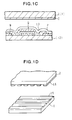
- Fig.1 C is a cross sectional view of transparent substrates, Fig.1 D is a schematic perspective view of transparent substrates, Fig.1 E is a schematic plan view of a liquid crystal cell, and Fig.1 F is a schematic plan view of a liquid crystal cell utilizing polarization memory film.
- Fig.2A shows a flow chart of a method of manufacturing a liquid crystal display according to another embodiment of this invention.
- Fig.2B is a graph showing an example of visual angle characteristics of a liquid crystal display according to the embodiment of this invention.
- Figs.3A to 3C are diagrams showing examples of multi-domain structures.
- Figs.4A and 4B show prior art, in which Fig.4a is a graph showing an example of visual angle characteristics of a liquid crystal display and Fig.4B is a diagram showing definitions of angles 0 and q).
- Before the description of the embodiments of this invention, prior work by the inventors and their colleague will first be described. Japanese Patent application 4-236652 (US patent application serial No. 8/115,441, European patent application No. 93114150.1), which is incorporated herein by reference, proposed a liquid crystal display which does not need any rubbing and can uniformalize the visual angle dependency.
- In this liquid crystal display, a liquid crystal layer is sandwiched between a pair of substrates having no orientation structure. Because the substrate has no orientation structure, the liquid crystal molecules in the cell forms multi-domain structure constituted by a multiplicity of micro domains. For example, when a area of several hundred micrometers square is considered, multi-domain structure is formed in this area.
- An example of the multi-domain structure is illustrated in Fig.3A. There are
many micro domains 30, in each of whichliquid crystal molecules 31 are aligned along a certain direction and exhibit parallel orientation. - When the multi-domain is seen widely as a whole, however, orientation of the
domains 30 are random. It can be considered that the orientations of liquid crystal molecules are directed to every direction on the substrate surface in a liquid crystal cell as a whole. - When such a liquid crystal cell is given a right angle twist by chiral agent and sandwiched between a pair of linear polarizers having crossed or parallel polarization axes, a liquid crystal display cell of positive or negative type can be obtained.
- In an ordinary twisted nematic liquid crystal display, the direction of the polarization axes of the polarizers are automatically determined by the direction of orientation of the liquid crystal molecules. In the liquid crystal display of no orientation structure, since the orientation directions are random in a liquid crystal cell as a whole (equal possibility in every direction), there is no need to align the orientation directions and the polarization axes of the polarizers.
- That is to say, provided that the polarization axes of a pair of polarizers are kept in orthogonal or parallel relationship, the polarization axes of the polarizers can be directed to any direction in the plane parallel to the liquid crystal cell substrate.
- In the manufacture of a liquid crystal display having no positive orientation structure, the distance between the substrates with no orientation structure is set at a value, for example, which enables a predetermined rotation of the polarization direction, e.g. 90 degrees, and a chiral nematic liquid crystal is injected between the substrates to form a liquid crystal cell. A pair of linear polarizers are disposed to sandwich the liquid crystal cell, without setting any particular relationship between the direction of polarization axes and the substrates, and then fixed. In this way, a liquid crystal display without rubbing treatment can be formed.
- Fig.1A shows a schematic cross sectional view of a liquid crystal display cell according to an embodiment of this invention. In the figure, a liquid crystal layer 3 of chiral nematic type or nematic type is sandwiched between a pair of
transparent glass substrates substrates linear polarizer plates - In this liquid crystal display cell, the orientation directions of the liquid crystal molecules at the interface between the liquid crystal layer and the substrates are directed uniformly to every direction when considered in the whole cell. When each micro domain is considered, the orientation directions of the liquid crystal molecules are directed along a certain direction at the interface. Fig.3A shows such orientation configuration.
- As shown in Fig.1 B, liquid crystal molecules take a twisted structure varying with the distance from the interface with a chirality defined by d/p, where d represents the thickness of the liquid crystal layer, and p represents the chiral pitch of the chiral nematic or nematic liquid crystal. Here, the nematic liquid crystal is represented by p = ∞, and the liquid crystal molecules in each micro domain are alined along the same direction regardless of the position along the thickness direction.
- Orientation and twisting of liquid crystal molecules take similar configuration in each micro domain of the multi-domain structure. As shown in Figs.lB and 3A, the orientation direction differs from micro domain to to micro domain. In the case of a chiral nematic liquid crystal, on the interface on the opposite side substrate, similar multi-domain structure but with every orientation direction rotated by the twist angle is produced.
- It is preferable to make a liquid crystal display cell to have a chiral pitch p of the liquid crystal and a thickness d of the liquid crystal layer which satisfy a relation, 0 = or < d/p < or = 0.75. Here, "A = or < B" means that A is approximately equal to or smaller than B. That is to say, values p and d are determined to have a polarization rotation angle, when expressed in degrees, from about 0 ° to about 270 °.
- In the case of a chiral nematic liquid crystal, values p and d are determined to satisfy, for example, 0.15 < d/p < 0.75. For example, a liquid crystal having a chiral pitch p defined by d/p = 0.25 - (corresponding to 90 degrees twisting) is injected between a pair of parallel
transparent glass substrates - As the liquid crystal material, for example, known nematic liquid crystals and known cholesteric liquid crystals can be used. When twisting nature is to be given, chiral agent may be added to a nematic liquid crystal.
- In the case of active drive system, as shown in Fig.1 C, driving element Q such as a thin film transistor (TFT) using amorphous silicon or polycrystalline silicon, wiring W formed of a metal such as chromium Cr, transparent pixel electrode P formed of indium-tin-oxide (ITO) etc. are formed on one glass substrats 1 (2). It is preferable to further coat these surfaces with an insulating
protective film 13. - Further constituents such as black stripe and color filter may also be formed. On the opposing substrate 2 (1), a common electrode C is formed on the whole surface.
- In the case of a simple matrix system, as shown in Fig.1D,
parallel electrodes transparent substrates substrates - Fig.1 E shows schematic appearance of an active or a simple matrix display. A
matrix display 20 has a multiplicity ofpixels 21 disposed in rows and columns. These pixels are defined by the transparent electrode P as shown in Fig.1 C or crossed areas of the crossed electrodes in Fig.1 D. In these matrix display, the direction ofcolumn 22 or direction ofrow 23 forms a reference direction. The display is designed to present an image when an observer views the display from the direction of column or row. The reference direction is illustrated by V in Fig.lA. - For example, when d/p = 0.25, a chiral nematic liquid crystal having a chirality pitch p satisfying the value d/p = 0.25 with respect to the gap d between the substrates is injected between the substrates. In each
micro domain 30 as shown in Fig.3A, liquid crystal molecules will take a configuration of 90 ° twist between two substrates. It is noted again that in a multi-domain structure, a multiplicity of domains are directed in every direction at the interface between the liquid crystal layer and a substrate. - Here, when injecting a liquid crystal, the temperature of the liquid crystal is preferably kept equal to or above N-I point which is the phace transition temperature between the nematic (N) phace and the isotropic (I) phace of the liquid crystal to keep the liquid crystal in the isotropic face. After injection, the temperature of the liquid crystal cell is gradually lowered below N-I point to bring the liquid crystal into a liquid crystal phace. This process will make the resultant liquid crystal cell better in display than injecting liquid crystal in the liquid crystal phace.
- Here, it is more preferable to also keep the temperature of the substrates before injection of the liquid crystal equal to or above N-I point and to inject the liquid crystal between the substrates. Then, the temperature of the substrates may be gradually lowered below N-I point. The resultant liquid crystal cell becomes better in display by this method.
- It can be expected that the liquid crystal in a cell without any orientation force will take a multi-domain structure, when considering that the liquid crystal in bulk state (a state without any external orientation force) takes a multi-domain state. Especially, it is considered that the tendency of taking a multi-domain structure becomes stronger and that the size of micro domains in a multi-domain structure when it is injected between the substrates while keeping the temperature of the liquid crystal equal to or above N-I point becomes more uniform.
- In the case of 90 ° twisted liquid crystal display cell, the orientation of the polarization axes of the polarizers are orthogonal in the case of positive display and parallel in the case of negative display. In the case of 0 ° twisted liquid crystal display, this relation is reversed. Although there is no reference direction of orientation such as rubbing direction on the substrate surface, there is a reference direction in a display determined in relation with the driving circuit, to define an observation direction. For example, in the case of matrix type display, the direction of row or column of the matrix will become the reference direction. In the case of segment type display such as seven segment display, the reference direction is defined by the direction from which the segment display is seen to recognize figure "8".
- Fig.2B shows an example of visual angle characteristics obtained in the liquid crystal display cell of Fig.lA. The direction of observation by an observer is set at the angle φ = 0 °, wherein the polarization axis of the polarizer on the observer side is directed 0 ° - 180°, and the polarization axis of the polarizer on the rear side is set 90 ° -270 ° (horizontal direction). Here, in the drawing, contours of equi-contrast ratio CR = 80, 40, 20, 10, and 5 are shown by solid curves.
- Compared to the characteristic of Fig.4A, it can be seen that a visual angle characteristics of very small directional dependency was obtained. It can be ascribed to the feature of not having any orientation structure on the substrates, thereby unifor- marizing respective directions.
- The equi-contrast curves CR, however, have direction dependency. Contrast is high in directions of polarization axes of the polarisers (direction of 0° - 180 ° and the direction of 90 ° - 270°), and is low in the intermediate angle regions therebetween. That is to say, there are regions of wide visual angle and regions of narrow visual angle.
- If the liquid crystal display is seen from the lower right direction (direction of 450) of Fig.2B, the vertical and the horizontal visual directions become narrow and the display becomes poor in usual observation. This tendency becomes more significant when the driving voltage becomes high.
- When the azimuthal direction is changed by 45 ° in Fig.2B, the positions of minimum contrast is changed to the maximum contrast. It can be seen that the directions of wide visual angle and narrow visual angle are separated by 45 degrees and distributed at a pitch of 90 degrees. When a display is seen in the usual state, it is said that an easily observable display can be obtained when the visual angles of vertical and horizontal directions are wide. The contrast in the vertical and horizontal directions (0 ° - 180 ° and 0° - 270 °) for the observer becomes high as shown in Fig.2B, when one of the polarization axes (transmission axis or absorption axis of the polarizer) is brought into coincidence with the reference direction of the display, which is the observation angle of the observer.
- Fig.2A is a flow chart of a method of manufacturing a liquid crystal display according to an embodiment of this invention. The respective steps can be achieved according to the conventional process.
- In step S1, electrode lines, driving elements, etc. are formed on a pair of glass substrates. No orientation film is formed on the substrates. Here, orientation film may be formed but no rubbing treatment is done thereon.
- In step S2, a pair of glass substrates are disposed face to face. Gap controlling members such as quartz balls are distributed between the sbstrates and the substrates are fixed at a predetermined gap. Periferies of the sbstrates are sealed and then a liquid crystal material is injected between the substrates. The gap of the liquid crystal cell is selected as described above.
- It is preferable in the step injecting a liquid crystal material into a cell that the liquid crystal is maintained at a temperature of N-I point or above. Heating the liquid crystal cell at the same time is more preferable as described above.
- In step S3, the liquid crystal injection port is sealed and a pair of polarizers are disposed to sandwich the liquid crystal cell substrates from the both sides. The two polarizers are kept in orthogonal relationship, for example, and the polarization axis or absorption axis of one of polarizers is set at the observation angle which is the reference direction of the display (the direction at which possibility of observing the display is highest, in this case 0°, 90°, 180 ° and 270 ° In this way, a liquid crystal display having such characteristics as shown in Fig.2B is formed.
- Multi-domain structures in the above embodiments can schematically be shown as in Fig.3A. Fig.3A is an enlarged plan view of the cell. A multiplicity of minute regions, i.e.
micro domains 30 are formed, andliquid crystal molecules 31 in eachmicro domain 30 are aligned substantially parallel in a certain direction as shown by arrows. Here, however, when the cell is seen as a whole or macroscopically, theliquid crystal molecules 31 are directed randomly at all the directions. It can be understood that the visual angle characteristics is effectively isotropic. - By varying the manufacturing conditions in various ways in the manufacturing process of a liquid crystal display cell in the afore-maintained embodiments, such orientation structures different from the multi-domain structure of Fig.3A can also be obtained.
- For example, as shown in Fig.3B, such a structure can be formed wherein
liquid crystal molecules 31 do not form particular domains, but change the orientation directions continuously. In the cell as a whole, the orientation directions are random and theliquid crystal molecules 31 are orientated to every direction at equal possibility. - Also, a structure which may be considered as a combination of Fig.3A and Fig.3B can be formed as shown in Fig.3C. That is to say,
micro domains 30 are distributed discretely, in each of which liquid crystal molecules are orietated at a uniform direction. Among themicro domains 30,liquid crystal molecules 31 are distributed, while varying the orientation directions continuously. In this case too, the orientation directions as a whole in the cell are random. - The above-mentioned effect of improved visual angle can be obtained with any of the structures as shown Fig.3A, 3B and 3C.
- The above-described embodiments do not employ any positive orientation treatment. In recent years, however, it was found that orientation treatment is possible without performing any rubbing treatment. For example, orientation treatment of minute regions can be done by irradiating light beem, utilizing polarization memory film.
- Fig.1 F shows an example of such positive orientation structure. The display surface is divided into a multiplicity of small regions. A polarization memory film is coated on a substrate and the polarization axis of exposing light is varied from region to region. Orientation structure is formed by such polarized light beam. A display cell is formed by utilizing at least one such substrate. The display cell include enough number of such small regions to exhibit orientation directions at effectively all directions at each pixel. It is necessary to include orientation directions of various directions so that each pixel can be considered to have random orientation directions by utilizing a substrate or substrates subjected to such orientation treatment. A multi-domain structure similar to those described above can be formed. Because no rubbing treatment is done, similar effects of performing no rubbing treatment can be obtained. Here, the polarization memory film can be formed by
- 1) silicon polyimide doped with diazo amine dye (Wayne M. Gibbons et al, NATURE Vol. 351-(1991) p.49,
- 2) polyvinyle alcohol (PVA) doped with azo- based dye (Yasufumi limuya et al, 18th Liquid Crystal Conference - The Chemical Society of Japan, 64th Automn annual meeting, p 34, September 11, 1992, or Jpn. J. Appln. Phys. Vol 32 (1993), pp L93-96),
- 3) photopolymerized photopolymer (Martin Schadt et al, Jpn. J. Appl. Phys. Vol. 31 (1992), pp 2155-2164), etc.
- Although this invention has been described along the embodiments thereof, this invention is not limited thereto. It will be apparent for those skilled in the art that various modifications, alternations, combinations, etc. can be done within the scope and the sprit of this invention as defined by the appended claims.
- It should be noted that the objects and advantages of the invention may be attained by means of any compatible combination(s) particularly pointed out in the items of the following summary of the invention and the appended claims.
-
- 1. A liquid crystal display comprising:
- a pair of transparent substrates, each having no uniform orientation direction, jointly constituting display pixels having a reference direction;
- a liquid crystal layer of chiral nematic liquid crystal or nematic liquid crystal sandwiched between said pair of transparent substrates;
- a pair of polarizers disposed on the both sides of said pair of transparent substrates and having polarization axes disposed in a predetermined mutual angular relationship, at least one of said polarizers having a transmission axis or absorption axis aligned with said reference direction.
- 2. A liquid crystal display wherein said pair of transparent substrates having no positive orientation structure.
- 3. A liquid crystal display wherein said pair of transparent substrates have positive orientation structure.
- 4. A liquid crystal display wherein said positive orientation structure is formed of a polarization memory film, and has orientation directions distributed to effectively all the directions in the plane parallel to the substrate at an equal possibility macroscopically.
- 5. A liquid crystal display wherein said polarization axes of the pair of polarizers are mutually orthogonal or parallel.
- 6. A liquid crystal display wherein the liquid crystal layer of said chiral nematic liquid crystal or nematic liquid crystal has a chiral pitch p, and a thickness d along a thickness direction sandwiched by said transparent substrates, and said p and d are selected to satisfy

- 7. A liquid crystal display wherein said liquid crystal layer comprises chiral nematic liquid crystal and said gap d and said chiral pitch p of the chiral nematic liquid crystal satisfy

- 8. A method of manufacturing a liquid crystal display comprising the steps of:
- preparing a pair of transparent substrates having no uniform orientation direction, and a chiral nematic or nematic liquid crystal;
- injecting said chiral nematic or nematic liquid crystalbetween said pair of transparent substrates to form a liquid crystal cell;
- disposing said liquid crystal cell between a pair of polarizers;
- arranging at least one of said pair of polarizers to have a transmission axis or an absorption axis alined with a observation direction, while keeping directions of polarization axes of said pair of polarizers in a predetermined mutual relationship.
- 9. A method of manufacturing a liquid crystal display wherein said step of injecting the liquid crystal between the pair of transparent substrates is achieved while keeping the temperature of the liquid crystal at least equal to N-I point of said liquid crystal.
- 10. A method of manufacturing a liquid crystal display wherein said step of injecting the liquid crystal between said pair of transparent substrate is achieved, while keeping the temperature of said transparent substrates at least equal to N-I point of said liquid crystal.
Claims (12)

Applications Claiming Priority (6)
| Application Number | Priority Date | Filing Date | Title |
|---|---|---|---|
| JP22498/93 | 1993-02-10 | ||
| JP2249893 | 1993-02-10 | ||
| JP2249893 | 1993-02-10 | ||
| JP29345593 | 1993-11-24 | ||
| JP5293455A JP2572537B2 (en) | 1993-02-10 | 1993-11-24 | Liquid crystal display device and manufacturing method thereof |
| JP293455/93 | 1993-11-24 |
Publications (3)
| Publication Number | Publication Date |
|---|---|
| EP0610923A2 true EP0610923A2 (en) | 1994-08-17 |
| EP0610923A3 EP0610923A3 (en) | 1995-05-10 |
| EP0610923B1 EP0610923B1 (en) | 2001-10-04 |
Family
ID=26359732
Family Applications (1)
| Application Number | Title | Priority Date | Filing Date |
|---|---|---|---|
| EP94102004A Expired - Lifetime EP0610923B1 (en) | 1993-02-10 | 1994-02-09 | Liquid crystal display of multi-domain structure |
Country Status (4)
| Country | Link |
|---|---|
| US (1) | US5479282A (en) |
| EP (1) | EP0610923B1 (en) |
| JP (1) | JP2572537B2 (en) |
| DE (1) | DE69428474T2 (en) |
Cited By (1)
| Publication number | Priority date | Publication date | Assignee | Title |
|---|---|---|---|---|
| US5712696A (en) * | 1994-02-17 | 1998-01-27 | Stanley Electric, Co., Ltd. | Manufacture of LCD device by transferring the orientation state from a parent substrate to a child substrate |
Families Citing this family (39)
| Publication number | Priority date | Publication date | Assignee | Title |
|---|---|---|---|---|
| US5670083A (en) * | 1994-02-23 | 1997-09-23 | Fuji Xerox Co., Ltd. | Optical element and process for producing the same |
| KR100228604B1 (en) * | 1994-11-17 | 1999-11-01 | 가네꼬 히사시 | Liquid crystal display device |
| US5959707A (en) * | 1995-04-24 | 1999-09-28 | Nec Corporation | Liquid crystal display having domains with different tilted-up directions as well as domains with different twist directions of lc molecules |
| US5831700A (en) * | 1995-05-19 | 1998-11-03 | Kent State University | Polymer stabilized four domain twisted nematic liquid crystal display |
| JP3506804B2 (en) * | 1995-05-23 | 2004-03-15 | 富士通ディスプレイテクノロジーズ株式会社 | LCD panel |
| JPH09297310A (en) * | 1996-05-01 | 1997-11-18 | Stanley Electric Co Ltd | Liquid crystal display element and its production |
| KR0182876B1 (en) | 1996-01-09 | 1999-05-01 | 구자홍 | Method for controlling pretilt direction for lcd cell |
| JP2872628B2 (en) | 1996-02-05 | 1999-03-17 | スタンレー電気株式会社 | Manufacturing method of liquid crystal display element |
| KR100206560B1 (en) * | 1996-05-14 | 1999-07-01 | 김광호 | Orientation method for lcd wide visual angle |
| US6191836B1 (en) | 1996-11-07 | 2001-02-20 | Lg Philips Lcd, Co., Ltd. | Method for fabricating a liquid crystal cell |
| JP3226830B2 (en) * | 1997-03-31 | 2001-11-05 | 日本電気株式会社 | Liquid crystal display |
| US6292296B1 (en) | 1997-05-28 | 2001-09-18 | Lg. Philips Lcd Co., Ltd. | Large scale polarizer and polarizer system employing it |
| KR100254857B1 (en) * | 1997-06-30 | 2000-05-01 | 김영환 | Method for aligning high molecular thin film and method for aligning liquid crystal using the same |
| US6184961B1 (en) * | 1997-07-07 | 2001-02-06 | Lg Electronics Inc. | In-plane switching mode liquid crystal display device having opposite alignment directions for two adjacent domains |
| KR100259258B1 (en) | 1997-11-21 | 2000-06-15 | 구본준 | Liquid crystal display device |
| US5953091A (en) * | 1998-04-09 | 1999-09-14 | Ois Optical Imaging Systems, Inc. | Multi-domain LCD and method of making same |
| US6124907A (en) | 1998-04-24 | 2000-09-26 | Ois Optical Imaging Systems, Inc. | Liquid crystal display with internal polarizer and method of making same |
| US6181401B1 (en) * | 1998-08-07 | 2001-01-30 | Honeywell International Inc. | Liquid crystal display with reduced off state luminance |
| JP2000122062A (en) * | 1998-10-13 | 2000-04-28 | Sony Corp | Optical element, its production, optical device and its production |
| US6061115A (en) * | 1998-11-03 | 2000-05-09 | International Business Machines Incorporation | Method of producing a multi-domain alignment layer by bombarding ions of normal incidence |
| US5982464A (en) * | 1998-12-16 | 1999-11-09 | Technoloogy Resource International Corporation | Multi-twist color liquid crystal display |
| KR100339332B1 (en) | 1999-02-08 | 2002-06-03 | 구본준, 론 위라하디락사 | Multi-domain liquid crystal display device |
| KR100301853B1 (en) * | 1999-03-25 | 2001-09-26 | 구본준, 론 위라하디락사 | Alignment layer for liquid crystal display device |
| KR100357214B1 (en) | 1999-04-21 | 2002-10-18 | 엘지.필립스 엘시디 주식회사 | Liquid crystal display device |
| US6313896B1 (en) | 1999-08-31 | 2001-11-06 | International Business Machines Corporation | Method for forming a multi-domain alignment layer for a liquid crystal display device |
| US7084087B2 (en) * | 1999-09-07 | 2006-08-01 | Abb Lummus Global Inc. | Zeolite composite, method for making and catalytic application thereof |
| KR100475107B1 (en) | 1999-10-14 | 2005-03-09 | 엘지.필립스 엘시디 주식회사 | A method of manufacturing a multi-domain liquid crystal display device |
| KR100565739B1 (en) | 2000-10-28 | 2006-03-29 | 엘지.필립스 엘시디 주식회사 | Photo-alignment Characteristic Material and Liquid Crystal Display Device fabricated with it |
| KR100595300B1 (en) | 2000-10-28 | 2006-07-03 | 엘지.필립스 엘시디 주식회사 | Photo-alignment Material and Liquid Crystal Display Device fabricated with it |
| AU2002322353A1 (en) * | 2001-07-02 | 2003-01-21 | Vladimir Kozenkov | Multilayer combined liquid crystal optical memory systems with means for recording and reading information |
| TWI271573B (en) * | 2001-08-22 | 2007-01-21 | Advanced Display Kk | Liquid crystal display device and method of producing the same |
| US7068336B2 (en) * | 2002-12-13 | 2006-06-27 | Lg.Philips Lcd Co., Ltd. | Liquid crystal display device having variable viewing angle |
| TWI255368B (en) * | 2003-03-19 | 2006-05-21 | Innolux Display Corp | Liquid crystal display and tis manufacting method |
| US7244627B2 (en) | 2003-08-25 | 2007-07-17 | Lg.Philips Lcd Co., Ltd. | Method for fabricating liquid crystal display device |
| KR101066483B1 (en) * | 2004-06-30 | 2011-09-22 | 엘지디스플레이 주식회사 | Liquid Crystal Display Device and Method for Manufacturing the Same |
| JP2006317656A (en) * | 2005-05-12 | 2006-11-24 | Dainippon Printing Co Ltd | Anisotropic optical element |
| JP4404118B2 (en) * | 2007-08-22 | 2010-01-27 | セイコーエプソン株式会社 | Liquid crystal display device and projector |
| TWI386722B (en) * | 2008-10-24 | 2013-02-21 | Taiwan Tft Lcd Ass | Optical sheet, display apparatus and fabricating method thereof |
| KR20160122305A (en) * | 2015-04-13 | 2016-10-24 | 삼성디스플레이 주식회사 | Liquid crystal display and manufacturing method thereof |
Citations (2)
| Publication number | Priority date | Publication date | Assignee | Title |
|---|---|---|---|---|
| EP0497619A2 (en) * | 1991-02-01 | 1992-08-05 | Fujitsu Limited | Liquid crystal display devices |
| EP0589264A2 (en) * | 1992-09-04 | 1994-03-30 | Stanley Electric Co., Ltd. | Liquid crystal display with non-rubbed substrates |
Family Cites Families (9)
| Publication number | Priority date | Publication date | Assignee | Title |
|---|---|---|---|---|
| US3503673A (en) * | 1967-09-14 | 1970-03-31 | Rca Corp | Reduction of turn-on delay in liquid crystal cell |
| DD146347A1 (en) * | 1979-09-26 | 1981-02-04 | Joachim Bergner | depolarizer |
| JPS56156817A (en) * | 1980-05-09 | 1981-12-03 | Hitachi Ltd | Liquid-crystal display element |
| JPS59111102A (en) * | 1982-12-16 | 1984-06-27 | Nippon Denso Co Ltd | Glare shielding type reflecting mirror |
| GB8616165D0 (en) * | 1986-07-02 | 1986-08-06 | Stc Plc | Liquid crystal cell |
| JPH03256922A (en) * | 1990-03-02 | 1991-11-15 | Nitta Ind Corp | Transfer device for lightweight object |
| US5216531A (en) * | 1990-08-28 | 1993-06-01 | Asahi Glass Company Ltd. | Projection type active matrix polymer dispersed liquid crystal display apparatus with particles of liquid crystal material randomly oriented |
| JP2945143B2 (en) * | 1990-12-07 | 1999-09-06 | 富士通株式会社 | Liquid crystal display |
| JPH04301618A (en) * | 1991-03-29 | 1992-10-26 | Nippon Telegr & Teleph Corp <Ntt> | Medium, method, and device for display and recording |
-
1993
- 1993-11-24 JP JP5293455A patent/JP2572537B2/en not_active Expired - Fee Related
-
1994
- 1994-02-04 US US08/191,554 patent/US5479282A/en not_active Expired - Fee Related
- 1994-02-09 DE DE69428474T patent/DE69428474T2/en not_active Expired - Fee Related
- 1994-02-09 EP EP94102004A patent/EP0610923B1/en not_active Expired - Lifetime
Patent Citations (2)
| Publication number | Priority date | Publication date | Assignee | Title |
|---|---|---|---|---|
| EP0497619A2 (en) * | 1991-02-01 | 1992-08-05 | Fujitsu Limited | Liquid crystal display devices |
| EP0589264A2 (en) * | 1992-09-04 | 1994-03-30 | Stanley Electric Co., Ltd. | Liquid crystal display with non-rubbed substrates |
Non-Patent Citations (1)
| Title |
|---|
| JOURNAL OF APPLIED PHYSICS, vol.74, no.3, 1 August 1993, NEW YORK US pages 2071 - 2075 Y.TOKO ET AL. 'AMO0RPHOUS TWISTED NEMATIC-LIQUID-CRYSTAL DISPLAYS FABRICATED BY NONRUBBING SHOWING WIDE AND UNIFORM VIEWING-ANGLE CHARACTERISTICS ACCOMPANYING EXCELLENT VOLTAGE HOLDING RATIOS' * |
Cited By (1)
| Publication number | Priority date | Publication date | Assignee | Title |
|---|---|---|---|---|
| US5712696A (en) * | 1994-02-17 | 1998-01-27 | Stanley Electric, Co., Ltd. | Manufacture of LCD device by transferring the orientation state from a parent substrate to a child substrate |
Also Published As
| Publication number | Publication date |
|---|---|
| US5479282A (en) | 1995-12-26 |
| DE69428474T2 (en) | 2002-06-06 |
| EP0610923A3 (en) | 1995-05-10 |
| EP0610923B1 (en) | 2001-10-04 |
| JP2572537B2 (en) | 1997-01-16 |
| JPH06294959A (en) | 1994-10-21 |
| DE69428474D1 (en) | 2001-11-08 |
Similar Documents
| Publication | Publication Date | Title |
|---|---|---|
| US5479282A (en) | Liquid crystal display of multi-domain structure | |
| US5453862A (en) | Rubbing-free (chiral) nematic liquid crystal display | |
| US5793459A (en) | Liquid crystal display of horizontal field type | |
| KR100241815B1 (en) | Liquid crystal electronic optical apparatus | |
| US5621558A (en) | Liquid crystal electro-optical device having alignment films for perpendicular alignment | |
| JPH09105941A (en) | Liquid crystal display device | |
| US5757454A (en) | Liquid crystal display device with homeotropic alignment in which two liquid crystal regions on the same subtrate have different pretilt directions because of rubbing | |
| JPH09197420A (en) | Liquid crystal element | |
| US5877831A (en) | Multi-domain LCD with subpixels having twist angles with opposite twist sense of within 60 and small/greater 90 degrees | |
| EP0610924B1 (en) | Multi-domain type liquid crystal display | |
| KR20110132043A (en) | Liquid crystal display device, method for manufacturing the same and method for manufacturing substrate for alignment of liquid crystal | |
| JP2621110B2 (en) | Liquid crystal display device and method of manufacturing the same | |
| JPH07333632A (en) | Liquid crystal display device | |
| JP2000131698A (en) | Liquid crystal display element and its production | |
| EP0775930A2 (en) | Liquid crystal display apparatus | |
| JP2809980B2 (en) | Liquid crystal display device and method of manufacturing the same | |
| JP2000356775A (en) | Liquid crystal display element and its production | |
| JPH0815707A (en) | Liquid crystal display element and its production | |
| JP3657708B2 (en) | Liquid crystal electro-optical device | |
| JPH09325339A (en) | Liquid crystal display element and its production | |
| KR0159130B1 (en) | Lcd device and its production | |
| KR100477132B1 (en) | Method for manufacturing liquid crystal display of using feroelectric liquid crystal material | |
| US7307678B2 (en) | Liquid crystal display and fabricating method thereof | |
| JPH08338995A (en) | Liquid crystal display panel and its production | |
| JPH07294934A (en) | Liquid crystal device |
Legal Events
| Date | Code | Title | Description |
|---|---|---|---|
| PUAI | Public reference made under article 153(3) epc to a published international application that has entered the european phase |
Free format text: ORIGINAL CODE: 0009012 |
|
| AK | Designated contracting states |
Kind code of ref document: A2 Designated state(s): DE FR GB IT NL |
|
| PUAL | Search report despatched |
Free format text: ORIGINAL CODE: 0009013 |
|
| AK | Designated contracting states |
Kind code of ref document: A3 Designated state(s): DE FR GB IT NL |
|
| 17P | Request for examination filed |
Effective date: 19951109 |
|
| 17Q | First examination report despatched |
Effective date: 19970707 |
|
| GRAG | Despatch of communication of intention to grant |
Free format text: ORIGINAL CODE: EPIDOS AGRA |
|
| GRAG | Despatch of communication of intention to grant |
Free format text: ORIGINAL CODE: EPIDOS AGRA |
|
| GRAH | Despatch of communication of intention to grant a patent |
Free format text: ORIGINAL CODE: EPIDOS IGRA |
|
| GRAH | Despatch of communication of intention to grant a patent |
Free format text: ORIGINAL CODE: EPIDOS IGRA |
|
| GRAA | (expected) grant |
Free format text: ORIGINAL CODE: 0009210 |
|
| AK | Designated contracting states |
Kind code of ref document: B1 Designated state(s): DE FR GB IT NL |
|
| PG25 | Lapsed in a contracting state [announced via postgrant information from national office to epo] |
Ref country code: IT Free format text: LAPSE BECAUSE OF FAILURE TO SUBMIT A TRANSLATION OF THE DESCRIPTION OR TO PAY THE FEE WITHIN THE PRESCRIBED TIME-LIMIT;WARNING: LAPSES OF ITALIAN PATENTS WITH EFFECTIVE DATE BEFORE 2007 MAY HAVE OCCURRED AT ANY TIME BEFORE 2007. THE CORRECT EFFECTIVE DATE MAY BE DIFFERENT FROM THE ONE RECORDED. Effective date: 20011004 |
|
| REF | Corresponds to: |
Ref document number: 69428474 Country of ref document: DE Date of ref document: 20011108 |
|
| REG | Reference to a national code |
Ref country code: GB Ref legal event code: IF02 |
|
| PGFP | Annual fee paid to national office [announced via postgrant information from national office to epo] |
Ref country code: GB Payment date: 20020213 Year of fee payment: 9 |
|
| PGFP | Annual fee paid to national office [announced via postgrant information from national office to epo] |
Ref country code: NL Payment date: 20020228 Year of fee payment: 9 Ref country code: DE Payment date: 20020228 Year of fee payment: 9 |
|
| ET | Fr: translation filed | ||
| PLBE | No opposition filed within time limit |
Free format text: ORIGINAL CODE: 0009261 |
|
| STAA | Information on the status of an ep patent application or granted ep patent |
Free format text: STATUS: NO OPPOSITION FILED WITHIN TIME LIMIT |
|
| 26N | No opposition filed | ||
| PG25 | Lapsed in a contracting state [announced via postgrant information from national office to epo] |
Ref country code: GB Free format text: LAPSE BECAUSE OF NON-PAYMENT OF DUE FEES Effective date: 20030209 |
|
| PG25 | Lapsed in a contracting state [announced via postgrant information from national office to epo] |
Ref country code: NL Free format text: LAPSE BECAUSE OF NON-PAYMENT OF DUE FEES Effective date: 20030901 |
|
| PG25 | Lapsed in a contracting state [announced via postgrant information from national office to epo] |
Ref country code: DE Free format text: LAPSE BECAUSE OF NON-PAYMENT OF DUE FEES Effective date: 20030902 |
|
| GBPC | Gb: european patent ceased through non-payment of renewal fee | ||
| NLV4 | Nl: lapsed or anulled due to non-payment of the annual fee |
Effective date: 20030901 |
|
| PG25 | Lapsed in a contracting state [announced via postgrant information from national office to epo] |
Ref country code: FR Free format text: LAPSE BECAUSE OF NON-PAYMENT OF DUE FEES Effective date: 20040430 |
|
| REG | Reference to a national code |
Ref country code: FR Ref legal event code: ST |
|
| PG25 | Lapsed in a contracting state [announced via postgrant information from national office to epo] |
Ref country code: FR Free format text: LAPSE BECAUSE OF NON-PAYMENT OF DUE FEES Effective date: 20020228 |