EP0613264A2 - Group modulator - Google Patents
Group modulator Download PDFInfo
- Publication number
- EP0613264A2 EP0613264A2 EP94400402A EP94400402A EP0613264A2 EP 0613264 A2 EP0613264 A2 EP 0613264A2 EP 94400402 A EP94400402 A EP 94400402A EP 94400402 A EP94400402 A EP 94400402A EP 0613264 A2 EP0613264 A2 EP 0613264A2
- Authority
- EP
- European Patent Office
- Prior art keywords
- frequency
- signal
- channel signal
- output
- circuit
- Prior art date
- Legal status (The legal status is an assumption and is not a legal conclusion. Google has not performed a legal analysis and makes no representation as to the accuracy of the status listed.)
- Granted
Links
- 238000013507 mapping Methods 0.000 claims abstract description 18
- 238000007493 shaping process Methods 0.000 claims abstract description 13
- 238000006243 chemical reaction Methods 0.000 claims description 8
- 238000000034 method Methods 0.000 description 27
- 230000008569 process Effects 0.000 description 26
- 238000010586 diagram Methods 0.000 description 10
- 230000000694 effects Effects 0.000 description 5
- 238000001228 spectrum Methods 0.000 description 5
- 239000000969 carrier Substances 0.000 description 3
- 230000008859 change Effects 0.000 description 3
- 238000004891 communication Methods 0.000 description 3
- 230000003044 adaptive effect Effects 0.000 description 2
- 230000005540 biological transmission Effects 0.000 description 2
- 238000010295 mobile communication Methods 0.000 description 2
- 230000010363 phase shift Effects 0.000 description 2
- 230000010267 cellular communication Effects 0.000 description 1
- 230000001413 cellular effect Effects 0.000 description 1
- 230000006870 function Effects 0.000 description 1
- 230000004048 modification Effects 0.000 description 1
- 238000012986 modification Methods 0.000 description 1
- 235000014366 other mixer Nutrition 0.000 description 1
- 238000011160 research Methods 0.000 description 1
- 238000005070 sampling Methods 0.000 description 1
- 230000001360 synchronised effect Effects 0.000 description 1
Images


Classifications
-
- H—ELECTRICITY
- H04—ELECTRIC COMMUNICATION TECHNIQUE
- H04J—MULTIPLEX COMMUNICATION
- H04J1/00—Frequency-division multiplex systems
- H04J1/02—Details
- H04J1/06—Arrangements for supplying the carrier waves ; Arrangements for supplying synchronisation signals
-
- H—ELECTRICITY
- H04—ELECTRIC COMMUNICATION TECHNIQUE
- H04J—MULTIPLEX COMMUNICATION
- H04J4/00—Combined time-division and frequency-division multiplex systems
- H04J4/005—Transmultiplexing
Definitions
- the present invention relates a group modulator, which is used in a digital radio communication system, for providing a plurality of modulated signals based upon a plurality of input data.
- a base station In a mobile communication system, a cellular communication system, and/or a personal communication system, a base station must transmit a plurality of radio signals simultaneously. The number of radio signals in each base station is lately increasing because of increase of traffic.
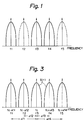
- Fig.1 shows a spectrum of modulated radio signals which are transmitted simultaneously, where f1 through f5 are center frequency of each radio signal.
- the solid lines f1, f3 and f4 show radio signal which is actually modulated, and the dotted lines f2 and f5 show the status that the modulated signals are not output.
- a digitally modulated signal which has a carrier signal modulated with base band data signal in digital form is produced by using a quadrature modurator which receives in-phase component (I-channel signal) and quadrature component (Q-channel signal).
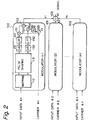
- Fig.2 shows a block diagram of a prior modulator which provides a plurality of radio signals.
- the numerals 100, 101 and 102 show a modulator which modulates a single input data
- 103 is an adder for adding the outputs of all the modulators.
- the output of the adder 103 is high frequency signal.
- the modulator 100 has a mapping circuit 112 which receives an input data #1, and provides I-channel signal and Q-channel signal for quadrature modulation according to instantaneous pattern of input data, and modulation system. Those I-channel signal and Q-channel signal are applied to the pulse shaping circuit 113 which restricts bandwidth of those signal.
- the I-channel signal and the Q-channel signal of the output of the pulse shaping circuit 113 are then applied to the digital-to-analog converters 131 and 132, respectively for the conversion of the signal from digital form to analog form.
- the outputs of the converters are applied to the mixers 151 and 152 which are a part of the quadrature modulator, through the low pass filters 141 and 142, respectively.
- the oscillator 155 provides the carrier frequency f1 which is designated by an external carrier designation signal #1.
- the carrier frequency f1 of the oscillator 155 is applied to the mixer or the multiplier 151 and the other mixer or the multiplier 152 through the ⁇ /2 phase shifter 154.
- the outputs of the mixers 151 and 152 are added in the adder 153, which provides the quadrature modulated signal which has the carrier frequency f1 modulated with the input data #1.
- the modulators 101 and 102 provide the quadrature modulated signals having the carrier frequencies f2 and f3, respectively, modulated with input data #2 and #3, respectively.
- the combination of the mixers 151 and 152, the adder 153, the oscillator 155 and the phase shifter 154 is a conventional quadrature modulator. Those modulated signals are added in the adder 103, to provide high frequency radio signal.
- each input signal is modulated in each modulator, in other words, a plurality of modulators equal to the number of input data are essential.
- the prior art of Fig.2 has the disadvantages that the structure of the apparatus is complicated as a plurality of modulators are essential, and that the amount of the traffic to be handled is limited by a number of modulators installed, in other words, it is impossible to follow adaptively the change of amount of traffic of input data.
- Digitally modulated signal S(t) is expressed as follows.
- S(t) A(t) cos( ⁇ i (t) + (w c + ⁇ w i )t) where A(t) is instantaneous value of base band signal in signal space diagram, and ⁇ i (t) is instantaneous phase angle.
- a modulated signal having the carrier angular frequency (w c + ⁇ w i ) may be produced by (1) frequency-shifting a base band signal ⁇ i (I-channel signal and Q-channel signal, respectively) by ⁇ w i , and (2) effecting quadrature modulation for angular carrier frequency w c with the frequency shifted signals.
- the resulated modulated signal is the same as the quadrature modulated signal of angular carrier frequency (w c + ⁇ w i ) with the non-shifted base band signal ⁇ i (t).
- Fig.4 shows a block diagram of the prior group modulator implementing above consideration.
- the symbols 61, 62, and 6n are a base band signal process circuit each of which receives an input data #1, #2, and #n, respectively.
- Each base band signal process circuit functions to serial-parallel conversion of an input data, mapping of signals allocating amplitude and phase of I-channel signal and Q-channel signal according to the pattern of the input data and the modulation system, to restrict bandwidth of the signals according to the transmission system, and to provide the frequency-shifted I-channel signal and Q-channel signal according to the externally supplied carrier control signal.
- the full adder 71 adds the I-channel signals of all the input data #1 through #n to provide the frequency-division multiplexed I-channel signal.
- the full adder 72 adds the Q-channel signals of all the input data #1 through #n to provide the frequency-division multiplexed Q-channel signal.
- the I-channel signal multiplexed by the full adder 71 is converted to analog form by the digital-to-analog (D/A) converter 31, the output of which is applied to the quadrature modulator 5 through the low pass filter 41, which restricts the bandwidth of the I-channel signal.
- the Q-channel data multiplexed by the full adder 72 is converted to analog form by the D/A converter 32, the output of which is applied, through the low pass filter 42, to the quadrature modulator 5.
- the multiplier 51 provides the product of the output of the low pass filter 41 and the carrier frequency f c which is supplied by the oscillator 55
- the multiplier 52 provides the product of the output of the low pass filter 42 and the carrier frequency f c with the phase shift by ⁇ /2 supplied by the oscillator 55 through the phase shifter 54.
- the adder 53 adds the outputs of the multipliers 51 and 52 to provide radio frequency signal RF, or intermediate frequency signal IF.
- the prior apparatus of Fig.4 has the disadvantage that a plurality of base band signal process circuits 61 through 6n must be essential, since each input data is separately processed to provide I-channel signal and Q-channel signal for the shift frequency ⁇ w i , so that a plurality of modulated signals each having specific carrier frequency are provided by adding all the I-channel signals and all the Q-channel signals.
- the number of input data is restricted to the number of the baseband signal process circuits.
- the prior apparatus has further disadvantage that some of the baseband signal process circuits would not operate when the number of input data is less than the number of the baseband signal process circuits. It should be appreciated that the number of input data is adaptive based upon instantaneous amount of traffic. Thus, the prior apparatus has the disadvantage that the system does not follow the increase and/or the decrease of the traffic.
- the object of the invention is to overcome the disadvantages and limitations of a prior group modulator by providing a new and improved group modulator.
- a group modulator for providing a plurality of frequency division multiplexed modulated signals each having different carrier frequency from one another relating to a plurality of input digital data
- a multiplexer for effecting time division multiplex of input digital data
- a mapping circuit for assigning amplitude and phase for each pattern of the multiplexed signal to provide I-channel signal and Q-channel signal according to the modulation system which modulates said input digital data
- a pulse shaping circuit for restricting bandwidth of output of said mapping circuit
- a frequency shift circuit receiving an external carrier control signal so that the frequency of the output of said pulse shaping circuit is shifted by the frequency defined by said carrier control signal; an accumulator for accumulating output of said frequency shift circuit during a predetermined period
- a digital-to-analog converter for converting output of said accumulator from digital form to analog form
- a modulator for modulating output of said digital-to-analog converter to provide frequency division multiplexed modulated high frequency signal.
- said modulator is a quadrature modulator.
- Fig.5 shows a block diagram of a group modulator according to the present invention.
- the numeral 1 shows a baseband signal process circuit which operates commonly for all the input data #1, through #n, where n is number of input channels.
- the baseband signal process circuit 1 has a time division multiplexer 11 which effects time division multiplex of all the input data sampling a value in a bit of each input data, and arranging the sampled values of all the input data in each bit period.
- the output of the multiplexer 11 is time divisional multiplexed signal. It should be appreciated that the presence of only one baseband signal process circuit 1 which operates on time divisional basis is the feature of the present invention.
- the numeral 12 is a mapping circuit which effects the mapping of the signals of the output of the multiplexer 11 according to the quadrature modulation system.
- the output of the mapping circuit 12 is the I-channel signal and the Q-channel signal for the quadrature modulation.
- serial-parallel conversion is carried out either in the multiplexer 11 or the mapping circuit 12 when input data is in serial form, so that parallel data is subject to mapping.
- the numeral 13 is a pulse shaping circuit for restricting bandwidth for effecting bandwidth restriction for I-channel signal and Q-channel signal of an output of the mapping circuit 12.
- the frequency shift circuit 14 is essentially implemented by a multiplier for providing product of shift frequency and I-channel signal (or Q-channel signal), or a ROM (read only memory) which stores the product of shift frequency and I-channel signal (or Q-channel signal).
- the output of the frequency shift circuit 14 is the output of the baseband signal process circuit.
- the numeral 21 is an accumulator for accumulating I-channel signal which is multiplexed, of the output of the baseband signal process circuit 1 for each bit period, so that all the component signals are added.
- the output of the accumulator 21 is essentially frequency division multiplexed I-channel signal.
- the numeral 22 is an accumulator operating similar to that of the accumulator 21, but for Q-channel signal.
- the outputs of the accumulators 21 and 22 are applied to the quadrature modulator 5 through the D/A converters 31 and 32, and the low pass filters 41 and 42.
- the former operate to convert signal format from digital form into analog form, and the latter operate to restrict frequency band.
- the members 21, 31 and 41 operate for I-channel signal, and the members 22, 32 and 42 operate for Q-channel signal.
- the quadrature modulator 5 has a pair of mixers or frequency converters 51 and 52, an adder 53 for adding outputs of the mixers 51 and 52, an oscillator 55 which provides radio frequency w c , and a phase shifter 54 which effects the phase shift by ⁇ /2 of the output of the oscillator 55 so that the mixers 51 and 52 receive the phase shifted radio frequencies by ⁇ /2.
- the structure and the operation of the quadrature modulator itself are conventional.
- the output of the adder 53 is radio frequency signal modulated with multiplexed signal, having the frequency spectrum as shown in Fig.3.
- the numeral 6 is a multiplicity control which provides a process clock signal C and a frame signal F to the baseband signal process circuit 1 and the accumulators 21 and 22, according to the designated number of multiplicity which is provided by an external circuit (not shown), so that the number of the multiplicity follows the amount of the traffic of input data.
- the multiplicity is large when the traffic is large, and the multiplicity is small when the traffic is small.
- Fig.8 shows two embodiments of a frequency shift circuit 14.
- Fig.8A shows the embodiment that the frequency shift circuit 14 is implemented essentially by digital multipliers
- Fig.8B shows the case that the frequency shift circuit 14 is essentially implemented by ROM's.
- the numerals 101, 102, 103 and 104 are a multiplier
- 105 is a ROM
- 106 and 107 are an adder.
- the ROM 105 which receives the carrier control signal (i), provides the instantaneous values of cos ⁇ w i t, sin ⁇ w i t, and -sin ⁇ w i t.
- the I-channel signal cos ⁇ i (t) of the output of the pulse shaping circuit 13 is applied to the multipliers 101 and 102, which also receive cos ⁇ w i t and sin ⁇ w i t of the output of the ROM 105, respectively, and provide the product cos ⁇ i (t)xcos ⁇ w i t, and cos ⁇ i (t)xsin ⁇ w i t, respectively.
- the multipliers 103 and 104 which receive the Q-channel signal sin ⁇ i (t) of the output of the pulse shaping circuit 13 provide sin ⁇ i (t)xsin ⁇ w i t and -sin ⁇ i (t)xcos ⁇ w i t, respectively.
- the adder 106 provides the sum of the outputs of the multipliers 101 and 103, and said sum is cos ( ⁇ i (t)+ ⁇ w i t).
- the adder 107 provides the sum of the outputs of the multipliers 102 and 104, and said sum is sin ( ⁇ i (t)+ ⁇ w i t).
- the outputs of the adders 106 and 107 provide the frequency shift of the I-channel signal and the Q-channel signal by the offset frequency ⁇ w i , which is defined by the carrier control signal (i).
- Fig.8B shows the other embodiment for implementing the frequency shift circuit 14.
- the numerals 121, 122, 123 and 124 are a ROM, each storing the value of cos ⁇ i (t)xcos ⁇ w i t, cos ⁇ i (t)xsin ⁇ w i t, sin ⁇ i (t)xcos ⁇ w i t, and -sin ⁇ i (t)xsin ⁇ w i t.
- the numeral 125 is a step generator, which indicates the step for reading the address of each ROM based upon the carrier control signal (i).
- the step for reading the ROM When the shift frequency designated by the carrier control signal is high, the step for reading the ROM is large, and when the shift frequency is low, the step for reading the ROM is small. For instance, when the step is 2, the ROM is read out in every other addreses, and the frequency read out of the ROM is twice of the frequency stored in the ROM.
- the ROM 121, 122, 123 or 124 is read out by the address indication cos ⁇ i (t) or sin ⁇ i (t), and the step supplied by the step generator, and provides the output similar to that of the multipliers 101 through 104, respectively, in Fig.8A. Then, the adders 126 and 127 operate similar to the adders 106 and 107 in Fig.8A, and therefore, the frequency shifted I-channel signal and the frequency shifted Q-channel signal are obtained.
- the frame clock signal F has a pulse at the beginning of a bit period T, and the period of the frame clock signal F is equal to that bit period T.
- the process clock signal C has n number of pulses in every bit period T, where n is the number of multiplicity.
- the process clock signal C and the frame clock signal F are synchronized with each other as shown in Fig.6B, and still preferably, the first pulse of the process clock signal C in each bit period T coincides with the frame clock pulse F.
- the multiplicity n is 5 in left portion of the figure,and n is 2 in the right portion of the figure.
- FIG.6 shows five series of input data #1 through #5, each applied to the multiplixer 11 in the baseband signal process circuit 1.
- Each of the input data #1 through #n has a series of digital bits D n-1 1, D n 1, D n+1 1, D n+2 1, et al.
- the period of the digital bits is T.
- the multiplexer 11 carries out the time division multiplex so that the digital bits of n number of input data at each bit period are packed in a bit period T as shown in Fig.6C, by using the frame clock signal F and the process clock signal C as shown in Fig.6B.
- the multiplicity is 5 and five input data #1 through #5 are packed.
- two input data #1 and #2 are packed as shown in right portion of Fig.6c.
- the mapping circuit 12 carries out the serial-parallel conversion of the multiplexed signal of the output of the multiplexer 11, and effects the mapping of the signal according to the pattern of the multiplexed input signal and the modulation system of the quadrature modulator.
- the output of the mapping circuit 12 has an I-channel signal and a Q-channel signal, each having the mapped amplitude and the phase.
- the pulse shaping circuit 13 effects the bandwidth restriction for those I-channel signal and Q-channel signal according to the transmission system.
- the outputs of the pulse shaping circuit 13 correspond to cos ⁇ i (t) and sin ⁇ i (t) in the equation (2).
- all the input data are frequency-shifted according to the carrier control signals.
- the outputs of the frequency shift circuit 14 correspond to cos ( ⁇ i (t)+ ⁇ w i t) and sin ( ⁇ i (t)+ ⁇ w i t) in the equation (2).
- the frequency shift circuit 14 is essentially implemented by a digital multiplier or a ROM (read only memory) as described in accordance with Fig.8.
- the amplitude information and the phase information of the I-channel signal and the Q-channel signal thus frequency shifted are output from the baseband signal process circuit 1.
- the baseband signal process circuit 1 operates in digital form, the period or the frequency spacing between the adjacent carrier frequencies is accurate and stable, and the switching of the carrier frequencies is quick and in high precise.
- the accumulators 21 and 22 operate to accumulate each of the I-channel signal and the Q-channel signal of the output of the baseband signal process circuit 1 for all the input data during the period T.
- the output of the accumulators 21 and 22 is essentially the frequency multiplexed signal.
- the output of the accumulators 21 and 22 are applied to the digital-to-analog converters 31 and 32, respectively.
- a digital-to-analog converter has a latch at the input of the same, the accumulated input signal is latched in the latch, and then, the latched signal is converted to analog form.
- the latched signal is shown in Fig.6D.
- the outputs of the D/A converters 31 and 32 are applied to the quadrature modulator 5 through the low pass filters 41 and 42, which remove high frequency component in the outputs of the D/A converters.
- the outputs of the low pass filters 41 and 42 correspond to ⁇ A(t) cos ( ⁇ i (t)+ ⁇ w i t), and ⁇ A(t) sin ( ⁇ i (t)+ ⁇ w i t) in the equation (3).
- the quadrature modulator 5 provides the quadrature modulated RF (radio frequency) signal or IF (intermediate frequency) signal.
- Fig.7 shows a block diagram of another embodiment of the present invention.
- the feature of Fig.7 as compared with that of Fig.5 is that the RF (or IF) signal is obtained through frequency conversion of one of I-channel signal and Q-channel signal which is frequency shifted and accumulated, instead of quadrature modulation.
- the numeral 90 is a mixer for frequency conversion
- 91 is an oscillator for providing local frequency w c to the mixer 90.
- the baseband process circuit 1 and the multiplicity control 6 in Fig.7 are the same as those in Fig.5, except that only one of I-channel signal and Q-channel signal is used.
- a frequency converter provides a pair of side bands on both sides of the carrier frequency
- a bandpass filter 92 for taking one of them and removing the other of them is provided at the output of the frequency converter.
- the output of the bandpass filter 92 is radio frequency signal which is frequency division multiplexed having a plurality of carriers.
- the switching of the multiplicity is also possible in the embodiment of Fig.7 by switching the number of process clock pulses F in each bit period T.
- a plurality of input data are first time division multiplexed, then, the I-channel signal and the Q-channel signal for quadrature modulation are obtained through the mapping operation of the time division multiplexed signal. Then, the I-channel signal and the Q-channel signal thus obtained are frequency-shifted according to each carrier frequency designated by the carrier control. Then, the frequency shifted I-channel signal and the frequency shifted Q-channel signal are accumulated for the whole bit period T so that the essentially frequency multiplexed signal is obtained. Then, the quadrature modulation or frequency conversion is effected for the accumulated signal.
- the communication system is adaptive to the change of the traffic with no change of hardware.
Abstract

Description
- The present invention relates a group modulator, which is used in a digital radio communication system, for providing a plurality of modulated signals based upon a plurality of input data.
- In a mobile communication system, a cellular communication system, and/or a personal communication system, a base station must transmit a plurality of radio signals simultaneously. The number of radio signals in each base station is lately increasing because of increase of traffic.
- Fig.1 shows a spectrum of modulated radio signals which are transmitted simultaneously, where f1 through f5 are center frequency of each radio signal. The solid lines f1, f3 and f4 show radio signal which is actually modulated, and the dotted lines f2 and f5 show the status that the modulated signals are not output.
- A digitally modulated signal which has a carrier signal modulated with base band data signal in digital form is produced by using a quadrature modurator which receives in-phase component (I-channel signal) and quadrature component (Q-channel signal).
- Fig.2 shows a block diagram of a prior modulator which provides a plurality of radio signals. In the figure, the
numerals adder 103 is high frequency signal. As the structure of themodulators 100 through 102 is the same as one another, themodulator 100 is described in detail. Themodulator 100 has amapping circuit 112 which receives aninput data # 1, and provides I-channel signal and Q-channel signal for quadrature modulation according to instantaneous pattern of input data, and modulation system. Those I-channel signal and Q-channel signal are applied to thepulse shaping circuit 113 which restricts bandwidth of those signal. The I-channel signal and the Q-channel signal of the output of thepulse shaping circuit 113 are then applied to the digital-to-analog converters mixers low pass filters oscillator 155 provides the carrier frequency f1 which is designated by an external carrierdesignation signal # 1. The carrier frequency f1 of theoscillator 155 is applied to the mixer or themultiplier 151 and the other mixer or themultiplier 152 through the ¶/2phase shifter 154. The outputs of themixers adder 153, which provides the quadrature modulated signal which has the carrier frequency f1 modulated with theinput data # 1. Similarly, themodulators input data # 2 and #3, respectively. The combination of themixers adder 153, theoscillator 155 and thephase shifter 154 is a conventional quadrature modulator. Those modulated signals are added in theadder 103, to provide high frequency radio signal. - It should be noted in Fig.2 that each input signal is modulated in each modulator, in other words, a plurality of modulators equal to the number of input data are essential.
- Therefore, the prior art of Fig.2 has the disadvantages that the structure of the apparatus is complicated as a plurality of modulators are essential, and that the amount of the traffic to be handled is limited by a number of modulators installed, in other words, it is impossible to follow adaptively the change of amount of traffic of input data.
- In order to solve those disadvantages, we first considered the group modulator shown in Fig.4, which was considered in our research laboratory, but is not commercially used. That is now explained.
- The frequency fi is considered that the reference carrier frequency fc (=wc/2¶; wc is angular frequency, ¶ is pi=90°) shifts by Δfi (=Δwi/2¶), as shown in Fig.3.
- Digitally modulated signal S(t) is expressed as follows.

where A(t) is instantaneous value of base band signal in signal space diagram, and φi(t) is instantaneous phase angle. - The equation (1) is transformed as follows.

- Therefore, it should be noted that a modulated signal having the carrier angular frequency (wc+Δwi) may be produced by (1) frequency-shifting a base band signal φi (I-channel signal and Q-channel signal, respectively) by Δwi, and (2) effecting quadrature modulation for angular carrier frequency wc with the frequency shifted signals. The resulated modulated signal is the same as the quadrature modulated signal of angular carrier frequency (wc+Δwi) with the non-shifted base band signal φi(t).
- A plurality of modulated signals having a plurality of carriers are expressed as follows.

- Therefore, it should be noted that a plurality of modulated signals are obtained by the steps of (1) frequency-shifting I-channel signal and Q-channel signal of each base band signal φi by the frequency Δwi (=2¶fi) which is defined by the externally supplied carrier control signal, (2) adding all the I-channel signals (and all the Q-channel signals), and (3) effecting quadrature modulation for angular frequency wc with the sum of the I-channel signals and the sum of the Q-channel signals.
- Fig.4 shows a block diagram of the prior group modulator implementing above consideration. In the figure, the
symbols input data # 1, #2, and #n, respectively. Each base band signal process circuit functions to serial-parallel conversion of an input data, mapping of signals allocating amplitude and phase of I-channel signal and Q-channel signal according to the pattern of the input data and the modulation system, to restrict bandwidth of the signals according to the transmission system, and to provide the frequency-shifted I-channel signal and Q-channel signal according to the externally supplied carrier control signal. Thefull adder 71 adds the I-channel signals of all theinput data # 1 through #n to provide the frequency-division multiplexed I-channel signal. Similarly, thefull adder 72 adds the Q-channel signals of all theinput data # 1 through #n to provide the frequency-division multiplexed Q-channel signal. - The I-channel signal multiplexed by the
full adder 71 is converted to analog form by the digital-to-analog (D/A)converter 31, the output of which is applied to thequadrature modulator 5 through thelow pass filter 41, which restricts the bandwidth of the I-channel signal. Similarly, the Q-channel data multiplexed by thefull adder 72 is converted to analog form by the D/A converter 32, the output of which is applied, through thelow pass filter 42, to thequadrature modulator 5. - In the
quadrature modulator 5, themultiplier 51 provides the product of the output of thelow pass filter 41 and the carrier frequency fc which is supplied by theoscillator 55, and themultiplier 52 provides the product of the output of thelow pass filter 42 and the carrier frequency fc with the phase shift by ¶/2 supplied by theoscillator 55 through thephase shifter 54. Theadder 53 adds the outputs of themultipliers - However, the prior apparatus of Fig.4 has the disadvantage that a plurality of base band
signal process circuits 61 through 6n must be essential, since each input data is separately processed to provide I-channel signal and Q-channel signal for the shift frequency Δwi, so that a plurality of modulated signals each having specific carrier frequency are provided by adding all the I-channel signals and all the Q-channel signals. - Further, the number of input data is restricted to the number of the baseband signal process circuits.
- The prior apparatus has further disadvantage that some of the baseband signal process circuits would not operate when the number of input data is less than the number of the baseband signal process circuits. It should be appreciated that the number of input data is adaptive based upon instantaneous amount of traffic. Thus, the prior apparatus has the disadvantage that the system does not follow the increase and/or the decrease of the traffic.
- The object of the invention is to overcome the disadvantages and limitations of a prior group modulator by providing a new and improved group modulator.
- It is also an object of the present invention to provide a group modulator which is simple in structure, having a single common baseband signal process circuit.
- It is also an object of the present invention to provide a group modulator in which a number of carriers is adaptively controlled depending upon amount of traffic of input data.
- The above and other objects are attained by a group modulator for providing a plurality of frequency division multiplexed modulated signals each having different carrier frequency from one another relating to a plurality of input digital data comprising; a multiplexer for effecting time division multiplex of input digital data; a mapping circuit for assigning amplitude and phase for each pattern of the multiplexed signal to provide I-channel signal and Q-channel signal according to the modulation system which modulates said input digital data; a pulse shaping circuit for restricting bandwidth of output of said mapping circuit; a frequency shift circuit receiving an external carrier control signal so that the frequency of the output of said pulse shaping circuit is shifted by the frequency defined by said carrier control signal; an accumulator for accumulating output of said frequency shift circuit during a predetermined period; a digital-to-analog converter for converting output of said accumulator from digital form to analog form; and a modulator for modulating output of said digital-to-analog converter to provide frequency division multiplexed modulated high frequency signal.
- Preferably, said modulator is a quadrature modulator.
- The foregoing and other objects, features, and attendant advantages of the present invention will be appreciated as the same become better understood by means of the following description and accompanying drawings wherein;
- Fig.1 shows frequency spectrum in high frequency band of frequency division multiplexed signal,
- Fig.2 is a block diagram of a prior group modulator,
- Fig.3 shows frequency spectrum in high frequency band showing another method for providing frequency division multiplexed signal,
- Fig.4 is a block diagram of another prior group modulator,
- Fig.5 is a block diagram of a group modulator according to the present invention,
- Fig.6 shows operational time chart of Fig.5,
- Fig.7 is a block diagram of another embodiment of the group modulator according to the present invention, and
- Fig.8 shows two embodiments of a block diagram of a frequency shift circuit in Fig.5.
- Fig.5 shows a block diagram of a group modulator according to the present invention. In the figure, the
numeral 1 shows a baseband signal process circuit which operates commonly for all theinput data # 1, through #n, where n is number of input channels. The basebandsignal process circuit 1 has atime division multiplexer 11 which effects time division multiplex of all the input data sampling a value in a bit of each input data, and arranging the sampled values of all the input data in each bit period. The output of themultiplexer 11 is time divisional multiplexed signal. It should be appreciated that the presence of only one basebandsignal process circuit 1 which operates on time divisional basis is the feature of the present invention. - The numeral 12 is a mapping circuit which effects the mapping of the signals of the output of the
multiplexer 11 according to the quadrature modulation system. The output of themapping circuit 12 is the I-channel signal and the Q-channel signal for the quadrature modulation. - It should be appreciated that serial-parallel conversion is carried out either in the
multiplexer 11 or themapping circuit 12 when input data is in serial form, so that parallel data is subject to mapping. - The numeral 13 is a pulse shaping circuit for restricting bandwidth for effecting bandwidth restriction for I-channel signal and Q-channel signal of an output of the
mapping circuit 12. - The numeral 14 is a frequency shift circuit which receives an offset frequency indication or a carrier control signal (i; i=l - n) for each input data, and the frequencies of the I-channel signal and Q-channel signal of the output of the
pulse shaping circuit 13 are shifted by the frequency defined by the carrier control signal (i). As the circuit operates in digital form, thefrequency shift circuit 14 is essentially implemented by a multiplier for providing product of shift frequency and I-channel signal (or Q-channel signal), or a ROM (read only memory) which stores the product of shift frequency and I-channel signal (or Q-channel signal). The output of thefrequency shift circuit 14 is the output of the baseband signal process circuit. - The numeral 21 is an accumulator for accumulating I-channel signal which is multiplexed, of the output of the baseband
signal process circuit 1 for each bit period, so that all the component signals are added. The output of theaccumulator 21 is essentially frequency division multiplexed I-channel signal. Similarly, the numeral 22 is an accumulator operating similar to that of theaccumulator 21, but for Q-channel signal. - The outputs of the
accumulators quadrature modulator 5 through the D/A converters members members - The
quadrature modulator 5 has a pair of mixers orfrequency converters adder 53 for adding outputs of themixers oscillator 55 which provides radio frequency wc, and aphase shifter 54 which effects the phase shift by ¶/2 of the output of theoscillator 55 so that themixers adder 53 is radio frequency signal modulated with multiplexed signal, having the frequency spectrum as shown in Fig.3. - The numeral 6 is a multiplicity control which provides a process clock signal C and a frame signal F to the baseband
signal process circuit 1 and theaccumulators - Fig.8 shows two embodiments of a
frequency shift circuit 14. Fig.8A shows the embodiment that thefrequency shift circuit 14 is implemented essentially by digital multipliers, and Fig.8B shows the case that thefrequency shift circuit 14 is essentially implemented by ROM's. - In Fig.8A, the
numerals ROM 105, which receives the carrier control signal (i), provides the instantaneous values of cos Δwit, sin Δwit, and -sin Δwit. The I-channel signal cos φi(t) of the output of thepulse shaping circuit 13 is applied to themultipliers ROM 105, respectively, and provide the product cos φi(t)xcosΔwit, and cos φi(t)xsinΔwit, respectively. Similarly, themultipliers pulse shaping circuit 13 provide sin φi(t)xsinΔwit and -sin φi(t)xcosΔwit, respectively. Theadder 106 provides the sum of the outputs of themultipliers adder 107 provides the sum of the outputs of themultipliers adders - Fig.8B shows the other embodiment for implementing the
frequency shift circuit 14. In Fig.8B, thenumerals - The
ROM multipliers 101 through 104, respectively, in Fig.8A. Then, theadders adders - Now, the operation of the apparatus of Fig.5 is described in accordance with Fig.6.
- The multiplicity control 6 receives the designation of the multiplicity n (n=2, 3, 4, et al), and provides the frame clock signal F and the process clock signal C, which are obtained by dividing a system clock signal according to the multiplicity n. The frame clock signal F has a pulse at the beginning of a bit period T, and the period of the frame clock signal F is equal to that bit period T. The process clock signal C has n number of pulses in every bit period T, where n is the number of multiplicity. Preferably, the process clock signal C and the frame clock signal F are synchronized with each other as shown in Fig.6B, and still preferably, the first pulse of the process clock signal C in each bit period T coincides with the frame clock pulse F. In the embodiment, the multiplicity n is 5 in left portion of the figure,and n is 2 in the right portion of the figure.
- In Fig.6, (a) shows five series of
input data # 1 through #5, each applied to themultiplixer 11 in the basebandsignal process circuit 1. Each of theinput data # 1 through #n has a series ofdigital bits D n-1¹,D n¹,D n+1¹,D n+2¹, et al. The period of the digital bits is T. - The multiplexer 11 carries out the time division multiplex so that the digital bits of n number of input data at each bit period are packed in a bit period T as shown in Fig.6C, by using the frame clock signal F and the process clock signal C as shown in Fig.6B. In left portion of Fig.6, the multiplicity is 5 and five
input data # 1 through #5 are packed. And, supposing that the designation of the multiplicity changed from 5 to 2, twoinput data # 1 and #2 are packed as shown in right portion of Fig.6c. - The
mapping circuit 12 carries out the serial-parallel conversion of the multiplexed signal of the output of themultiplexer 11, and effects the mapping of the signal according to the pattern of the multiplexed input signal and the modulation system of the quadrature modulator. The output of themapping circuit 12 has an I-channel signal and a Q-channel signal, each having the mapped amplitude and the phase. - The
pulse shaping circuit 13 effects the bandwidth restriction for those I-channel signal and Q-channel signal according to the transmission system. The outputs of thepulse shaping circuit 13 correspond to cos φi(t) and sin φi(t) in the equation (2). - The
frequency shift circuit 14 receives a carrier control signal (i) where i=1 through n. The example of the carrier frequencies for each input data are 300 kHz, 600 kHz, 900 kHz et al. Therefore, it should be appreciated that i=1 (carrier control signal is 1) designates the carrier frequency of 300 kHz, and i=2 designates 600 kHz, i=3 designates 900 kHz, et al. - In Fig.6C, the first data signal #1 (Dn-1¹) is frequency-shifted by 300 kHz as designated by the carrier control signal (i=1) in the first 1/5 duration of the bit period T. Secondly, the second data signal #2 (Dn-1²) is frequency-shifted by 600 kHz as designated by the carrier control signal (i=2) in the second 1/5 duration of the bit period T. Similarly, all the input data are frequency-shifted according to the carrier control signals. The outputs of the
frequency shift circuit 14 correspond to cos (φi(t)+Δwit) and sin (φi(t)+Δwit) in the equation (2). As all the signals are in digital form, thefrequency shift circuit 14 is essentially implemented by a digital multiplier or a ROM (read only memory) as described in accordance with Fig.8. - The amplitude information and the phase information of the I-channel signal and the Q-channel signal thus frequency shifted are output from the baseband
signal process circuit 1. - It should be appreciated that since the baseband
signal process circuit 1 operates in digital form, the period or the frequency spacing between the adjacent carrier frequencies is accurate and stable, and the switching of the carrier frequencies is quick and in high precise. - The
accumulators signal process circuit 1 for all the input data during the period T. The output of theaccumulators - The output of the
accumulators analog converters - The outputs of the D/
A converters quadrature modulator 5 through the low pass filters 41 and 42, which remove high frequency component in the outputs of the D/A converters. The outputs of the low pass filters 41 and 42 correspond to Σ A(t) cos (φi(t)+Δwit), and Σ A(t) sin (φi(t)+Δwit) in the equation (3). - The
quadrature modulator 5 provides the quadrature modulated RF (radio frequency) signal or IF (intermediate frequency) signal. - Fig.7 shows a block diagram of another embodiment of the present invention. The feature of Fig.7 as compared with that of Fig.5 is that the RF (or IF) signal is obtained through frequency conversion of one of I-channel signal and Q-channel signal which is frequency shifted and accumulated, instead of quadrature modulation. In Fig.7, the numeral 90 is a mixer for frequency conversion, and 91 is an oscillator for providing local frequency wc to the
mixer 90. Thebaseband process circuit 1 and the multiplicity control 6 in Fig.7 are the same as those in Fig.5, except that only one of I-channel signal and Q-channel signal is used. Only one set of anaccumulator 21, a D/A converter 31 and alow pass filter 41 are used in Fig.7, although a pair of those members are used in Fig.5. Since a frequency converter provides a pair of side bands on both sides of the carrier frequency, abandpass filter 92 for taking one of them and removing the other of them is provided at the output of the frequency converter. The output of thebandpass filter 92 is radio frequency signal which is frequency division multiplexed having a plurality of carriers. - The switching of the multiplicity is also possible in the embodiment of Fig.7 by switching the number of process clock pulses F in each bit period T.
- As described above in detail, according to the present invention, a plurality of input data are first time division multiplexed, then, the I-channel signal and the Q-channel signal for quadrature modulation are obtained through the mapping operation of the time division multiplexed signal. Then, the I-channel signal and the Q-channel signal thus obtained are frequency-shifted according to each carrier frequency designated by the carrier control. Then, the frequency shifted I-channel signal and the frequency shifted Q-channel signal are accumulated for the whole bit period T so that the essentially frequency multiplexed signal is obtained. Then, the quadrature modulation or frequency conversion is effected for the accumulated signal.
- Therefore, it should be appreciated that the increase and/or the decrease of the number of input data or the multiplicity n is carried out simply by changing the designation of the multiplicity to the multiplicity control 6. No additional modulator and no additional baseband signal process circuit is necessary when a number of input data increases.
- It should be appreciated that when the multiplicity n is small because of low traffic, the circuits in the apparatus operate with low rate, and therefore, the power consumption in the circuits is low.
- As the spectrum of Fig.3 of the present invention is the same as that of a prior art of Fig.1, no modification of a receiver is necessary when the present invention is used in a transmitter.
- When the present invention is used in a transmitter in a base station in a cellular telephone system and/or a mobile communication system, the communication system is adaptive to the change of the traffic with no change of hardware.
- From the foregoing it will now be apparent that a new and improved group modulator has been found. It should be appreciated of course that the embodiments disclosed are merely illustrative and are not intended to limit the scope of the invention. Reference should be made to the appended claims therefore rather than the specification as indicating the scope of the invention.
Claims (9)
- (1) A group modulator for providing a plurality of frequency division multiplexed modulated signals having different carrier frequency from one another relating to a plurality of input digital data comprising;
a time division multiplexer for effecting time division multiplex of input digital data,
a mapping circuit for assigning amplitude and phase for each pattern of the multiplexed signal to provide I-channel signal and Q-channel signal according to the modulation system which modulates said input digital data,
a pulse shaping circuit for restricting bandwidth of output of said mapping circuit,
a frequency shift circuit receiving an external carrier control signal so that the frequency of said output of said pulse shaping circuit is shifted by the frequency defined by said carrier control signal,
an accumulator for accumulating output of said frequency shift circuit during a predetermined period,
a digital-to-analog converter for converting output of said accumulator from digital form to analog form, and
a modulator for modulating output of said digital-to-analog converter to provide frequency division multiplexed modulated high frequency signal. - (2) A group modulator according to claim 1, wherein said modulator is a quadrature modulator, and said mapping circuit provides I-channel signal and Q-channel signal having phase difference by 90° for quadrature modulation.
- (3) A group modulator according to claim 1, wherein said digital-to-analog converter has a latch circuit to keep an input signal to the level at the initial stage of the conversion.
- (4) A group modulator according to claim 1, wherein a low pass filter is provided between output of said digital-to-analog converter and said modulator.
- (5) A group modulator according to claim 1, wherein a multiplicity control is provided so that a number of multiplicity in said time division multiplexer is adjustably controlled according to a multiplicity signal which is applied to said multiplicity control from an outside circuit.
- (6) A group modulator according to claim 1, wherein said modulator is a frequency converter, and a bandpass filter is provided at output of said frequency converter to remove undesirable side band generated in said frequency converter.
- (7) A group modulator according to claim 5, wherein multiplicity is adjusted according to amount of traffic of input data.
- (8) A group modulator according to claim 1, wherein said frequency shift circuit is implemented by a plurality of digital multipliers each providing product of input signal of said frequency shift circuit and instantaneous value of said shift frequency, and an adder for providing sum of outputs of two of said digital multipliers.
- (9) A group modulator according to claim 1, wherein said frequency shift circuit is implemented by a plurality of ROM's which store product of input signal of said frequency shift circuit and instantaneous value of said shift frequency, and an adder for providing sum of outputs of two of said ROM's.
Applications Claiming Priority (3)
| Application Number | Priority Date | Filing Date | Title |
|---|---|---|---|
| JP3791093 | 1993-02-26 | ||
| JP37910/93 | 1993-02-26 | ||
| JP3791093 | 1993-02-26 |
Publications (3)
| Publication Number | Publication Date |
|---|---|
| EP0613264A2 true EP0613264A2 (en) | 1994-08-31 |
| EP0613264A3 EP0613264A3 (en) | 1995-11-08 |
| EP0613264B1 EP0613264B1 (en) | 2003-10-22 |
Family
ID=12510704
Family Applications (1)
| Application Number | Title | Priority Date | Filing Date |
|---|---|---|---|
| EP94400402A Expired - Lifetime EP0613264B1 (en) | 1993-02-26 | 1994-02-24 | Group modulator |
Country Status (3)
| Country | Link |
|---|---|
| US (1) | US5430711A (en) |
| EP (1) | EP0613264B1 (en) |
| DE (1) | DE69433255T2 (en) |
Cited By (2)
| Publication number | Priority date | Publication date | Assignee | Title |
|---|---|---|---|---|
| WO1996024205A1 (en) * | 1995-01-31 | 1996-08-08 | Ericsson Inc. | Method and apparatus for generating plural quadrature modulated carriers |
| WO1997002673A1 (en) * | 1995-06-30 | 1997-01-23 | Scientific-Atlanta, Inc. | Group modulator for a broadband communications system |
Families Citing this family (13)
| Publication number | Priority date | Publication date | Assignee | Title |
|---|---|---|---|---|
| US5748679A (en) * | 1995-04-28 | 1998-05-05 | Trw Inc. | Modulated clock MSK modulator for high data rate applications |
| US5930687A (en) * | 1996-09-30 | 1999-07-27 | Usa Digital Radio Partners, L.P. | Apparatus and method for generating an AM-compatible digital broadcast waveform |
| FR2777145B1 (en) * | 1998-04-02 | 2000-04-28 | Alsthom Cge Alcatel | BROADBAND MULTI-CARRIER MODULATOR AND CORRESPONDING PROGRAMMING METHOD |
| US20030147471A1 (en) * | 1998-10-05 | 2003-08-07 | Simon Marvin K. | Cross correlated trellis coded quatrature modulation transmitter and system |
| US20020039388A1 (en) * | 2000-02-29 | 2002-04-04 | Smart Kevin J. | High data-rate powerline network system and method |
| KR20020040903A (en) * | 2000-08-21 | 2002-05-30 | 다니구찌 이찌로오, 기타오카 다카시 | π/2 PHASE SHIFTER |
| JP4322268B2 (en) * | 2006-07-21 | 2009-08-26 | テクトロニクス・インターナショナル・セールス・ゲーエムベーハー | Signal generating apparatus and method |
| JP5161444B2 (en) * | 2006-08-11 | 2013-03-13 | テクトロニクス・インコーポレイテッド | Jitter characteristic analysis program and jitter characteristic table or graph display method |
| US8223069B2 (en) * | 2008-09-05 | 2012-07-17 | Lg Electronics Inc. | Network assisted positioning |
| US8868013B2 (en) * | 2009-10-20 | 2014-10-21 | Electronics And Telecommunications Research Institute | Apparatus and method for transmitting/receiving signal |
| CN102130697B (en) * | 2010-01-20 | 2015-05-27 | 华为技术有限公司 | Receiver, transmitter and feedback device, transceiver and signal processing method |
| KR102342740B1 (en) * | 2014-09-15 | 2021-12-23 | 삼성전자주식회사 | Method and transmitter for transmitting and receiving a signal |
| CN111886811B (en) | 2018-02-01 | 2023-05-23 | 日本电信电话株式会社 | Transmitting apparatus, wireless communication system, and transmitting method |
Citations (3)
| Publication number | Priority date | Publication date | Assignee | Title |
|---|---|---|---|---|
| US3912870A (en) * | 1972-12-07 | 1975-10-14 | Cit Alcatel | Digital group modulator |
| US4881241A (en) * | 1988-02-24 | 1989-11-14 | Centre National D'etudes Des Telecommunications | Method and installation for digital communication, particularly between and toward moving vehicles |
| WO1992006546A1 (en) * | 1990-10-05 | 1992-04-16 | Motorola, Inc. | Frequency agile tdma communications system |
Family Cites Families (3)
| Publication number | Priority date | Publication date | Assignee | Title |
|---|---|---|---|---|
| US4780884A (en) * | 1986-03-03 | 1988-10-25 | American Telephone And Telegraph Company, At&T Bell Laboratories | Suppressed double-sideband communication system |
| JPH0335640A (en) * | 1989-07-03 | 1991-02-15 | Nippon Telegr & Teleph Corp <Ntt> | Orthogonal modulator |
| US5237586A (en) * | 1992-03-25 | 1993-08-17 | Ericsson-Ge Mobile Communications Holding, Inc. | Rake receiver with selective ray combining |
-
1994
- 1994-02-24 EP EP94400402A patent/EP0613264B1/en not_active Expired - Lifetime
- 1994-02-24 DE DE69433255T patent/DE69433255T2/en not_active Expired - Fee Related
- 1994-02-25 US US08/201,989 patent/US5430711A/en not_active Expired - Fee Related
Patent Citations (3)
| Publication number | Priority date | Publication date | Assignee | Title |
|---|---|---|---|---|
| US3912870A (en) * | 1972-12-07 | 1975-10-14 | Cit Alcatel | Digital group modulator |
| US4881241A (en) * | 1988-02-24 | 1989-11-14 | Centre National D'etudes Des Telecommunications | Method and installation for digital communication, particularly between and toward moving vehicles |
| WO1992006546A1 (en) * | 1990-10-05 | 1992-04-16 | Motorola, Inc. | Frequency agile tdma communications system |
Non-Patent Citations (1)
| Title |
|---|
| IEEE COMMUNICATIONS MAGAZINE, vol. 28, no. 5, May 1990 US, pages 5-14, J.A.C. BINGHAM 'Multicarrier Modulation for Data Transmission: An Idea Whose Time Has Come' * |
Cited By (4)
| Publication number | Priority date | Publication date | Assignee | Title |
|---|---|---|---|---|
| WO1996024205A1 (en) * | 1995-01-31 | 1996-08-08 | Ericsson Inc. | Method and apparatus for generating plural quadrature modulated carriers |
| US5638401A (en) * | 1995-01-31 | 1997-06-10 | Ericsson Inc. | Method and apparatus for generating plural quadrature modulated carriers |
| WO1997002673A1 (en) * | 1995-06-30 | 1997-01-23 | Scientific-Atlanta, Inc. | Group modulator for a broadband communications system |
| US5825829A (en) * | 1995-06-30 | 1998-10-20 | Scientific-Atlanta, Inc. | Modulator for a broadband communications system |
Also Published As
| Publication number | Publication date |
|---|---|
| EP0613264B1 (en) | 2003-10-22 |
| US5430711A (en) | 1995-07-04 |
| DE69433255D1 (en) | 2003-11-27 |
| EP0613264A3 (en) | 1995-11-08 |
| DE69433255T2 (en) | 2004-04-29 |
Similar Documents
| Publication | Publication Date | Title |
|---|---|---|
| US5430711A (en) | Group modulator | |
| US4761798A (en) | Baseband phase modulator apparatus employing digital techniques | |
| US4783779A (en) | Frequency assignment system in FDMA communication system | |
| US5818813A (en) | Orthogonal frequency division multiplexing transmission system and transmitter and receiver adapted to the same | |
| US5220557A (en) | Multiple use digital transmitter/transceiver with time multiplexing | |
| EP0802644A2 (en) | Variable-bandwith frequency division multiplex communication system | |
| US5978421A (en) | Envelope control unit and digital modulator using the envelope control unit and digital modulation method | |
| EP0687074A2 (en) | Spread spectrum communication method | |
| US5627499A (en) | Digital modulator and upconverter having single-bit delta-sigma data converters | |
| EP0681382A2 (en) | Digital modulator for cellular base stations | |
| US4812786A (en) | Method and system for providing precise multi-function modulation | |
| KR0137529B1 (en) | Quadrature quadrature | |
| EP0881806B1 (en) | Frame structure with a plurality of modulation formats | |
| US5148127A (en) | Biphase shift keying modulation circuit having constant envelope characteristics | |
| US5373532A (en) | π/4 quadrature phase shift keying modulator | |
| EP1045561A2 (en) | Frequency correction in multicarrier receivers | |
| EP1057281B1 (en) | Compensation for phase errors caused by clock jitter in a cdma communication system | |
| JP2001127736A (en) | Radio frequency transmitter of cdma type mobile communication base station system | |
| US5444708A (en) | Time-division multiplex radio transmission apparatus | |
| KR20050030756A (en) | Method and process for implementing wideband multicarrier | |
| JPH06318923A (en) | Batch modulator | |
| KR960007663B1 (en) | Cdma | |
| EP0064728A2 (en) | Multiple phase digital modulator | |
| JP2568345B2 (en) | Digital modulator | |
| US5825805A (en) | Spread spectrum communication system |
Legal Events
| Date | Code | Title | Description |
|---|---|---|---|
| PUAI | Public reference made under article 153(3) epc to a published international application that has entered the european phase |
Free format text: ORIGINAL CODE: 0009012 |
|
| 17P | Request for examination filed |
Effective date: 19940228 |
|
| AK | Designated contracting states |
Kind code of ref document: A2 Designated state(s): DE FR |
|
| PUAL | Search report despatched |
Free format text: ORIGINAL CODE: 0009013 |
|
| AK | Designated contracting states |
Kind code of ref document: A3 Designated state(s): DE FR |
|
| RAP1 | Party data changed (applicant data changed or rights of an application transferred) |
Owner name: NIPPON TELEGRAPH AND TELEPHONE CORPORATION |
|
| 17Q | First examination report despatched |
Effective date: 19990126 |
|
| GRAH | Despatch of communication of intention to grant a patent |
Free format text: ORIGINAL CODE: EPIDOS IGRA |
|
| GRAS | Grant fee paid |
Free format text: ORIGINAL CODE: EPIDOSNIGR3 |
|
| GRAA | (expected) grant |
Free format text: ORIGINAL CODE: 0009210 |
|
| AK | Designated contracting states |
Kind code of ref document: B1 Designated state(s): DE FR |
|
| REF | Corresponds to: |
Ref document number: 69433255 Country of ref document: DE Date of ref document: 20031127 Kind code of ref document: P |
|
| PGFP | Annual fee paid to national office [announced via postgrant information from national office to epo] |
Ref country code: DE Payment date: 20040217 Year of fee payment: 11 |
|
| PGFP | Annual fee paid to national office [announced via postgrant information from national office to epo] |
Ref country code: FR Payment date: 20040225 Year of fee payment: 11 |
|
| ET | Fr: translation filed | ||
| PLBE | No opposition filed within time limit |
Free format text: ORIGINAL CODE: 0009261 |
|
| STAA | Information on the status of an ep patent application or granted ep patent |
Free format text: STATUS: NO OPPOSITION FILED WITHIN TIME LIMIT |
|
| 26N | No opposition filed |
Effective date: 20040723 |
|
| PG25 | Lapsed in a contracting state [announced via postgrant information from national office to epo] |
Ref country code: DE Free format text: LAPSE BECAUSE OF NON-PAYMENT OF DUE FEES Effective date: 20050901 |
|
| PG25 | Lapsed in a contracting state [announced via postgrant information from national office to epo] |
Ref country code: FR Free format text: LAPSE BECAUSE OF NON-PAYMENT OF DUE FEES Effective date: 20051031 |
|
| REG | Reference to a national code |
Ref country code: FR Ref legal event code: ST Effective date: 20051031 |