EP0631394A1 - Liquid crystal display apparatus - Google Patents
Liquid crystal display apparatus Download PDFInfo
- Publication number
- EP0631394A1 EP0631394A1 EP94304204A EP94304204A EP0631394A1 EP 0631394 A1 EP0631394 A1 EP 0631394A1 EP 94304204 A EP94304204 A EP 94304204A EP 94304204 A EP94304204 A EP 94304204A EP 0631394 A1 EP0631394 A1 EP 0631394A1
- Authority
- EP
- European Patent Office
- Prior art keywords
- switches
- data
- data line
- bits
- liquid crystal
- Prior art date
- Legal status (The legal status is an assumption and is not a legal conclusion. Google has not performed a legal analysis and makes no representation as to the accuracy of the status listed.)
- Ceased
Links
Images

Classifications
-
- G—PHYSICS
- G09—EDUCATION; CRYPTOGRAPHY; DISPLAY; ADVERTISING; SEALS
- G09G—ARRANGEMENTS OR CIRCUITS FOR CONTROL OF INDICATING DEVICES USING STATIC MEANS TO PRESENT VARIABLE INFORMATION
- G09G3/00—Control arrangements or circuits, of interest only in connection with visual indicators other than cathode-ray tubes
- G09G3/20—Control arrangements or circuits, of interest only in connection with visual indicators other than cathode-ray tubes for presentation of an assembly of a number of characters, e.g. a page, by composing the assembly by combination of individual elements arranged in a matrix no fixed position being assigned to or needed to be assigned to the individual characters or partial characters
- G09G3/34—Control arrangements or circuits, of interest only in connection with visual indicators other than cathode-ray tubes for presentation of an assembly of a number of characters, e.g. a page, by composing the assembly by combination of individual elements arranged in a matrix no fixed position being assigned to or needed to be assigned to the individual characters or partial characters by control of light from an independent source
- G09G3/36—Control arrangements or circuits, of interest only in connection with visual indicators other than cathode-ray tubes for presentation of an assembly of a number of characters, e.g. a page, by composing the assembly by combination of individual elements arranged in a matrix no fixed position being assigned to or needed to be assigned to the individual characters or partial characters by control of light from an independent source using liquid crystals
- G09G3/3611—Control of matrices with row and column drivers
- G09G3/3685—Details of drivers for data electrodes
- G09G3/3688—Details of drivers for data electrodes suitable for active matrices only
-
- G—PHYSICS
- G09—EDUCATION; CRYPTOGRAPHY; DISPLAY; ADVERTISING; SEALS
- G09G—ARRANGEMENTS OR CIRCUITS FOR CONTROL OF INDICATING DEVICES USING STATIC MEANS TO PRESENT VARIABLE INFORMATION
- G09G3/00—Control arrangements or circuits, of interest only in connection with visual indicators other than cathode-ray tubes
- G09G3/20—Control arrangements or circuits, of interest only in connection with visual indicators other than cathode-ray tubes for presentation of an assembly of a number of characters, e.g. a page, by composing the assembly by combination of individual elements arranged in a matrix no fixed position being assigned to or needed to be assigned to the individual characters or partial characters
- G09G3/34—Control arrangements or circuits, of interest only in connection with visual indicators other than cathode-ray tubes for presentation of an assembly of a number of characters, e.g. a page, by composing the assembly by combination of individual elements arranged in a matrix no fixed position being assigned to or needed to be assigned to the individual characters or partial characters by control of light from an independent source
- G09G3/36—Control arrangements or circuits, of interest only in connection with visual indicators other than cathode-ray tubes for presentation of an assembly of a number of characters, e.g. a page, by composing the assembly by combination of individual elements arranged in a matrix no fixed position being assigned to or needed to be assigned to the individual characters or partial characters by control of light from an independent source using liquid crystals
- G09G3/3611—Control of matrices with row and column drivers
- G09G3/3696—Generation of voltages supplied to electrode drivers
-
- G—PHYSICS
- G09—EDUCATION; CRYPTOGRAPHY; DISPLAY; ADVERTISING; SEALS
- G09G—ARRANGEMENTS OR CIRCUITS FOR CONTROL OF INDICATING DEVICES USING STATIC MEANS TO PRESENT VARIABLE INFORMATION
- G09G2310/00—Command of the display device
- G09G2310/02—Addressing, scanning or driving the display screen or processing steps related thereto
- G09G2310/0243—Details of the generation of driving signals
- G09G2310/0248—Precharge or discharge of column electrodes before or after applying exact column voltages
-
- G—PHYSICS
- G09—EDUCATION; CRYPTOGRAPHY; DISPLAY; ADVERTISING; SEALS
- G09G—ARRANGEMENTS OR CIRCUITS FOR CONTROL OF INDICATING DEVICES USING STATIC MEANS TO PRESENT VARIABLE INFORMATION
- G09G2310/00—Command of the display device
- G09G2310/02—Addressing, scanning or driving the display screen or processing steps related thereto
- G09G2310/0264—Details of driving circuits
- G09G2310/027—Details of drivers for data electrodes, the drivers handling digital grey scale data, e.g. use of D/A converters
-
- G—PHYSICS
- G09—EDUCATION; CRYPTOGRAPHY; DISPLAY; ADVERTISING; SEALS
- G09G—ARRANGEMENTS OR CIRCUITS FOR CONTROL OF INDICATING DEVICES USING STATIC MEANS TO PRESENT VARIABLE INFORMATION
- G09G2320/00—Control of display operating conditions
- G09G2320/06—Adjustment of display parameters
- G09G2320/066—Adjustment of display parameters for control of contrast
-
- G—PHYSICS
- G09—EDUCATION; CRYPTOGRAPHY; DISPLAY; ADVERTISING; SEALS
- G09G—ARRANGEMENTS OR CIRCUITS FOR CONTROL OF INDICATING DEVICES USING STATIC MEANS TO PRESENT VARIABLE INFORMATION
- G09G3/00—Control arrangements or circuits, of interest only in connection with visual indicators other than cathode-ray tubes
- G09G3/20—Control arrangements or circuits, of interest only in connection with visual indicators other than cathode-ray tubes for presentation of an assembly of a number of characters, e.g. a page, by composing the assembly by combination of individual elements arranged in a matrix no fixed position being assigned to or needed to be assigned to the individual characters or partial characters
- G09G3/2007—Display of intermediate tones
- G09G3/2011—Display of intermediate tones by amplitude modulation
-
- G—PHYSICS
- G09—EDUCATION; CRYPTOGRAPHY; DISPLAY; ADVERTISING; SEALS
- G09G—ARRANGEMENTS OR CIRCUITS FOR CONTROL OF INDICATING DEVICES USING STATIC MEANS TO PRESENT VARIABLE INFORMATION
- G09G3/00—Control arrangements or circuits, of interest only in connection with visual indicators other than cathode-ray tubes
- G09G3/20—Control arrangements or circuits, of interest only in connection with visual indicators other than cathode-ray tubes for presentation of an assembly of a number of characters, e.g. a page, by composing the assembly by combination of individual elements arranged in a matrix no fixed position being assigned to or needed to be assigned to the individual characters or partial characters
- G09G3/2007—Display of intermediate tones
- G09G3/2014—Display of intermediate tones by modulation of the duration of a single pulse during which the logic level remains constant
Definitions
- the present invention relates to a liquid crystal display apparatus including a driver for driving data lines of the liquid crystal display panel.
- TFT/LCD thin-film transistor liquid crystal displays
- analog type driver an analog data signal representing gradations of respective pixels is sampled and held using switches and capacitors, buffered in operational amplifiers (voltage followers) and then output to data lines of a display panel.
- the analog type driver can produce continuous (i.e., infinite) gradations.
- there are various problems such as low accuracy of output voltages, low operation speed and large power consumption, and thus the analog type driver is rarely used for computer displays.
- the digital type driver a plurality of power supplies having different potentials are connected to each data line through their respective switches and a voltage signal is supplied to each data line by selectively turning on one of the switches in accordance with the input data. Since no linear circuit is used, the digital type driver consumes little power. Furthermore, since the power supply voltages are output as they are, output voltages are highly accurate and the operation speed can easily be increased. However, to increase display gradations, it is necessary to increase the number of power supply terminals to provide potentials corresponding to the respective necessary gradations and the number of switches corresponding to the respective power supply terminals.
- Japanese patent application PEPA No. 61-58008 published on December 9, 1986 discloses a voltage generation circuit for producing a plurality of differing voltage outputs from a pair of power supplies in the above type of driver.
- a plurality of intermediate voltages between the voltages of the pair of power supplies are generated by dividing the interval between the two power supply voltages using a plurality of resistors based on the operation of selection switches. By connecting capacitors at positions where the voltage difference across the terminals of the division resistor is constant, the problem of the output waveform distortion is solved without increasing the power consumption.
- an object of the present invention is to provide a liquid crystal display apparatus which can perform multi-gradation display without increasing the chip area of the driver, i.e., with a smaller number of circuit elements.
- the present invention provides a liquid crystal display apparatus comprising a liquid crystal display panel having a plurality of display cells arranged in a matrix and a plurality of data lines connected to the display cells, means for receiving input data comprising a plurality of bits per pixel, said plurality of bits representing gradations of a pixel to be displayed on the panel, and a drive means for driving the data lines by potential signals corresponding to the respective gradations represented by the input data, the drive means comprising: at least two switches connected to a power supply for selectively supplying reference potentials corresponding to at least two different graduation values to the data line; and decoding means responsive to the input data to control said two switches so that the switches are alternately turned on and off at a predetermined cycle so as to supply a potential to said data line, obtained from said reference potential, corresponding to a gradation represented by the input data.
- switches are connected to respective power supplies having reference potentials corresponding to at least two different gradations to allow the reference potentials to be selectively supplied to a data line of the liquid crystal display panel through the switches.
- a decoder is provided which decodes input data and controls the switches so that the switches are alternately turned on and off at a predetermined cycle at a ratio in which the reference potentials are proportionally divided by a potential corresponding to a gradation represented by the input data.
- multiple graduations can be obtained by means of a driver which needs only two switches to produce the output voltage having an arbitrary level between two potentials. A small chip area is thus achieved.
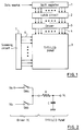
- FIG. 1 is a block diagram schematically showing a multi-gradation thin-film transistor liquid crystal display (TFT/LCD) according to the present invention.
- this type of display consists of a shift register 1 for converting, to parallel data, serial input data (which represents display gradations of respective pixels) of a line to be displayed that is received from a data source such as the CPU of a computer, a latch circuit 2 for latching the parallel-converted input data, a driver 5 for driving data lines 4 of a thin-film transistor liquid crystal display 3 by output potentials having magnitudes corresponding to the respective input data of the latch circuit 2, and a scanning circuit (gate driver) 7 for sequentially supplying scanning signals to gate lines 6 of the display panel 3.
- Each display cell on the gate line 6 being driven by the scanning circuit 7 exhibits gradations corresponding to the output potential of the associated data line.
- the input data represents gradations of the respective pixels of one line.
- the input data consists of 6 bits per pixel. Therefore, the driver 5 should be able to generate potentials of 64 different magnitudes to properly represent the 6-bit gradation data.
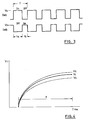
- FIG. 2 is a schematic circuit diagram which shows a driver circuit embodying the principle of the invention. Switches connected to two respective power sources supplying the terminals of a driver IC having different potentials are turned on and off at a predetermined cycle at a time ratio in which the two potentials are proportionally divided by a potential corresponding to a gradation represented by the input data, so that the output potential necessary to produce the gradation represented by the input data is supplied to the cell.
- the potentials of the two power supply terminals are denoted by V a and V b
- the switches connected to the respective terminals are denoted by SW a and SW b
- a load resistance and a capacitance of the data line of the display panel are denoted by R and C
- the output potential given to the cell is denoted by V c .
- the time necessary to charge up the resistor and the capacitor of the data line is denoted by T
- on-periods of the respective switches SW a and SW b in a predetermined cycle t are denoted by t a and t b , where t « T.
- the output potential V c changes as shown in Figure 4 because of the existence of an RC circuit consisting of the load resistor and the capacitor of the data line, and settles after a lapse of time period T.
- T and t are longer than about 30 ⁇ sec. and 3 ⁇ sec., respectively.
- V a and V b are 5 V and 4 V, respectively and the time ratio t a /t b is an integer-to-integer ratio from 6:0 to 0:6, the output voltage V c takes values listed in the following table, as derived from Eq. 1.
- FIG 5 schematically shows an embodiment of an invention for driving one data line in the driver 5 (see Figure 1).
- the driver 5 has this type of circuit in the number of data lines 4.
- the driver 5 includes a plurality of switches SW1-SW17 that are connected to respective power supply terminals having a plurality of potentials V1-V17 (e.g., 1 to 17 V), and is constructed so as to selectively supply the potentials of the respective terminals to the data line 4.
- the upper 4-bit data is input to a first decoder 11 and the lower 2-bit data is input to a second decoder 12.
- the first decoder 11 converts the upper 4-bit data to a signal for selecting one switch SW i and the following switch SW i+1 from the switches SW1-SW17.
- the second decoder 12 converts the lower 2-bit data into a signal indicating the ratio (time ratio) between the on-periods t a and t b of the respective selected switches SW i and SW i+1 .
- the switches SW i and SW i+1 are turned on and off at a predetermined cycle (e.g., 3 ⁇ sec.) at the time ratio indicated by the output signal of the decoder 12. After this operation is repeated for the predetermined period (e.g., 30 ⁇ sec.) necessary to charge up the data line, the output potential to be applied to the cell settles, as described above, to the potential corresponding to the 6-bit gradation data.
- the output potential takes a value corresponding to the gradation data.
Abstract
A multi-gradation thin-film liquid crystal display (TFT/LCD) includes a data line driver which does not cause an increase in the chip area, (i.e., which is constituted of a smaller number of circuit elements). Power supplies having respective reference potentials Va and Vb corresponding to at least two different gradations, and switches SWa and SWb for selectively supplying the respective potentials to a data line, are provided in a driver IC for driving the data lines of a TFT/LCD panel. If an output potential corresponding to an arbitrary gradation between the two predetermined gradations is denoted by Vc, the output potential Vc is supplied to the data line by being turned on and off the switches SWa and SWb alternately at a predetermined cycle in a ratio in which the potential Vc proportionally divides the potentials Va and Vb. Therefore, the output potential corresponding to an arbitrary gradation between the two predetermined gradations can be obtained simply by properly changing the ratio of turning the two switches on and off.
Description
- The present invention relates to a liquid crystal display apparatus including a driver for driving data lines of the liquid crystal display panel.
- Drivers for multi-gradation thin-film transistor liquid crystal displays (TFT/LCD) are generally classified into analog type and digital type. In the analog type driver, an analog data signal representing gradations of respective pixels is sampled and held using switches and capacitors, buffered in operational amplifiers (voltage followers) and then output to data lines of a display panel.
- In theory, the analog type driver can produce continuous (i.e., infinite) gradations. In practice, however, there are various problems such as low accuracy of output voltages, low operation speed and large power consumption, and thus the analog type driver is rarely used for computer displays.
- On the other hand, in the digital type driver, a plurality of power supplies having different potentials are connected to each data line through their respective switches and a voltage signal is supplied to each data line by selectively turning on one of the switches in accordance with the input data. Since no linear circuit is used, the digital type driver consumes little power. Furthermore, since the power supply voltages are output as they are, output voltages are highly accurate and the operation speed can easily be increased. However, to increase display gradations, it is necessary to increase the number of power supply terminals to provide potentials corresponding to the respective necessary gradations and the number of switches corresponding to the respective power supply terminals.
- Japanese patent application PEPA No. 61-58008 published on December 9, 1986 discloses a voltage generation circuit for producing a plurality of differing voltage outputs from a pair of power supplies in the above type of driver. In this circuit, a plurality of intermediate voltages between the voltages of the pair of power supplies are generated by dividing the interval between the two power supply voltages using a plurality of resistors based on the operation of selection switches. By connecting capacitors at positions where the voltage difference across the terminals of the division resistor is constant, the problem of the output waveform distortion is solved without increasing the power consumption.
- However, in the above conventional circuit, a number of resistors and switches need to be provided on a chip. Therefore, to increase the number of display gradations, the chip area unavoidably increases. In practice, it is difficult to perform multi-gradation display of more than about 16 gradations using a driver formed on a small chip.
- Accordingly, an object of the present invention is to provide a liquid crystal display apparatus which can perform multi-gradation display without increasing the chip area of the driver, i.e., with a smaller number of circuit elements.
- Accordingly, the present invention provides a liquid crystal display apparatus comprising a liquid crystal display panel having a plurality of display cells arranged in a matrix and a plurality of data lines connected to the display cells, means for receiving input data comprising a plurality of bits per pixel, said plurality of bits representing gradations of a pixel to be displayed on the panel, and a drive means for driving the data lines by potential signals corresponding to the respective gradations represented by the input data, the drive means comprising: at least two switches connected to a power supply for selectively supplying reference potentials corresponding to at least two different graduation values to the data line; and decoding means responsive to the input data to control said two switches so that the switches are alternately turned on and off at a predetermined cycle so as to supply a potential to said data line, obtained from said reference potential, corresponding to a gradation represented by the input data.
- Thus in accordance with the present invention, switches are connected to respective power supplies having reference potentials corresponding to at least two different gradations to allow the reference potentials to be selectively supplied to a data line of the liquid crystal display panel through the switches. A decoder is provided which decodes input data and controls the switches so that the switches are alternately turned on and off at a predetermined cycle at a ratio in which the reference potentials are proportionally divided by a potential corresponding to a gradation represented by the input data.
- In a preferred embodiment comprising a thin-film transistor liquid crystal display, multiple graduations can be obtained by means of a driver which needs only two switches to produce the output voltage having an arbitrary level between two potentials. A small chip area is thus achieved.
- A preferred embodiment of the invention will now be described, by way of example only, with reference to the accompanying drawings in which:
- Figure 1 is a block diagram of a multi-gradation TFT/LCD;
- Figure 2 is a schematic circuit diagram showing a relationship between a driver and a data line;
- Figure 3 is a timing chart showing on/off cycles of two switches;
- Figure 4 is a graph showing how an output voltage changes; and
- Figure 5 is a block diagram of a driver according to an embodiment.
- Figure 1 is a block diagram schematically showing a multi-gradation thin-film transistor liquid crystal display (TFT/LCD) according to the present invention. In general, this type of display consists of a
shift register 1 for converting, to parallel data, serial input data (which represents display gradations of respective pixels) of a line to be displayed that is received from a data source such as the CPU of a computer, alatch circuit 2 for latching the parallel-converted input data, adriver 5 for driving data lines 4 of a thin-film transistorliquid crystal display 3 by output potentials having magnitudes corresponding to the respective input data of thelatch circuit 2, and a scanning circuit (gate driver) 7 for sequentially supplying scanning signals to gate lines 6 of thedisplay panel 3. Each display cell on the gate line 6 being driven by the scanning circuit 7 exhibits gradations corresponding to the output potential of the associated data line. - The input data represents gradations of the respective pixels of one line. For example, in the case of a 64-gradation display, the input data consists of 6 bits per pixel. Therefore, the
driver 5 should be able to generate potentials of 64 different magnitudes to properly represent the 6-bit gradation data. - Figure 2 is a schematic circuit diagram which shows a driver circuit embodying the principle of the invention. Switches connected to two respective power sources supplying the terminals of a driver IC having different potentials are turned on and off at a predetermined cycle at a time ratio in which the two potentials are proportionally divided by a potential corresponding to a gradation represented by the input data, so that the output potential necessary to produce the gradation represented by the input data is supplied to the cell.
- To describe the above principle more specifically, the potentials of the two power supply terminals are denoted by Va and Vb, the switches connected to the respective terminals are denoted by SWa and SWb, a load resistance and a capacitance of the data line of the display panel are denoted by R and C, and the output potential given to the cell is denoted by Vc. Furthermore, the time necessary to charge up the resistor and the capacitor of the data line is denoted by T, and on-periods of the respective switches SWa and SWb in a predetermined cycle t are denoted by ta and tb, where t « T. When the switches SWa and SWb are repeatedly turned on and off at a time ratio as shown in Figure 3, the output potential Vc changes as shown in Figure 4 because of the existence of an RC circuit consisting of the load resistor and the capacitor of the data line, and settles after a lapse of time period T. In this case, the output potential Vc takes a value obtained by proportionally dividing the potentials Va and Vb in the time ratio ta/tb. That is,

- It is apparent from Eq. 1 that if either ta or tb is made 0 in the on/off operation of the switches SWa and SWb, the output potential Vc becomes equal to Vb or Va.
- It is desirable that T and t not be longer than about 30 µsec. and 3 µsec., respectively. For this reason, where Va and Vb are 5 V and 4 V, respectively and the time ratio ta/tb is an integer-to-integer ratio from 6:0 to 0:6, the output voltage Vc takes values listed in the following table, as derived from Eq. 1.
ta/tb Vc 6:0 5.0 5:1 4.8 4:2 4.7 3:3 4.5 2:4 4.3 1:5 4.2 0:6 4.0 - In the above manner, generation of an output voltage Vc with an arbitrary level can be obtained between the two power supply potentials by properly changing the time ratio ta/tb.
- Figure 5 schematically shows an embodiment of an invention for driving one data line in the driver 5 (see Figure 1). The
driver 5 has this type of circuit in the number of data lines 4. Thedriver 5 includes a plurality of switches SW₁-SW₁₇ that are connected to respective power supply terminals having a plurality of potentials V₁-V₁₇ (e.g., 1 to 17 V), and is constructed so as to selectively supply the potentials of the respective terminals to the data line 4. - Of the 6-bit gradation data supplied from the latch circuit 2 (see Figure 1), the upper 4-bit data is input to a first decoder 11 and the lower 2-bit data is input to a
second decoder 12. - Using an incorporated conversion table 13, the first decoder 11 converts the upper 4-bit data to a signal for selecting one switch SWi and the following switch SWi+1 from the switches SW₁-SW₁₇.
- Using an incorporated conversion table 14, the
second decoder 12 converts the lower 2-bit data into a signal indicating the ratio (time ratio) between the on-periods ta and tb of the respective selected switches SWi and SWi+1. Under the control of a controller (not shown), the switches SWi and SWi+1 are turned on and off at a predetermined cycle (e.g., 3 µsec.) at the time ratio indicated by the output signal of thedecoder 12. After this operation is repeated for the predetermined period (e.g., 30 µsec.) necessary to charge up the data line, the output potential to be applied to the cell settles, as described above, to the potential corresponding to the 6-bit gradation data. - As described above, since the on/off time ratio of the two switches is set in accordance with the gradation data, the output potential takes a value corresponding to the gradation data.
Claims (5)
- A liquid crystal display apparatus comprising a liquid crystal display panel (3) having a plurality of display cells arranged in a matrix and a plurality of data lines (4) connected to the display cells, means (1, 2) for receiving input data comprising a plurality of bits per pixel, said plurality of bits representing gradations of a pixel to be displayed on the panel, and a drive means (5) for driving the data lines by potential signals corresponding to the respective gradations represented by the input data, the drive means comprising:
at least two switches (SWa, SWb) connected to a power supply for selectively supplying reference potentials corresponding to at least two different graduation values to the data line; and
decoding means (11, 12, 13, 14) responsive to the input data to control said two switches so that the switches are alternately turned on and off at a predetermined cycle so as to supply a potential to said data line, obtained from said reference potential, corresponding to a gradation represented by the input data. - Apparatus as claimed in claim 1, wherein said power supply comprises at least n+1 terminals for supplying n reference potentials having equal potential differences.
- Apparatus as claimed in claim 2, comprising n+1 switches connected to the n+1 terminals.
- Apparatus as claimed in any preceding claim, wherein said decoding means comprises a first table to be referenced for selecting switches connected to terminals having two consecutive reference potentials of said n+1 terminals in accordance with first selected bits of the plurality of bits, and a second table to be referenced for determining a ratio between on and off periods of the two selected switches in accordance with the second selected bits of said plurality of bits.
- Apparatus as claimed in any preceding claim, wherein the predetermined cycle has a period no greater than 10 percent of the time necessary to charge up the data line.
Applications Claiming Priority (2)
| Application Number | Priority Date | Filing Date | Title |
|---|---|---|---|
| JP153823/93 | 1993-06-24 | ||
| JP15382393A JPH0720821A (en) | 1993-06-24 | 1993-06-24 | Multigradation thin-film transistor liquid-crystal display |
Publications (1)
| Publication Number | Publication Date |
|---|---|
| EP0631394A1 true EP0631394A1 (en) | 1994-12-28 |
Family
ID=15570875
Family Applications (1)
| Application Number | Title | Priority Date | Filing Date |
|---|---|---|---|
| EP94304204A Ceased EP0631394A1 (en) | 1993-06-24 | 1994-06-10 | Liquid crystal display apparatus |
Country Status (3)
| Country | Link |
|---|---|
| EP (1) | EP0631394A1 (en) |
| JP (1) | JPH0720821A (en) |
| KR (1) | KR950001376A (en) |
Cited By (2)
| Publication number | Priority date | Publication date | Assignee | Title |
|---|---|---|---|---|
| EP0694900A3 (en) * | 1994-07-27 | 1996-04-10 | Sharp Kk | An active matrix type display device and a method for driving the same |
| GB2307584A (en) * | 1995-11-27 | 1997-05-28 | Varintelligent | A driver for a liquid crystal display |
Families Citing this family (6)
| Publication number | Priority date | Publication date | Assignee | Title |
|---|---|---|---|---|
| KR100486228B1 (en) * | 1998-01-06 | 2005-06-16 | 삼성전자주식회사 | Contrast voltage control circuit for driving liquid crystal device |
| KR100438966B1 (en) * | 2001-12-28 | 2004-07-03 | 엘지.필립스 엘시디 주식회사 | A liquid crystal display device applying common voltage having different phase and a method of operating thereof |
| JP3882678B2 (en) * | 2002-05-21 | 2007-02-21 | ソニー株式会社 | Display device |
| JP2006119417A (en) * | 2004-10-22 | 2006-05-11 | Renesas Technology Corp | Driving device for display apparatus |
| WO2007072904A1 (en) * | 2005-12-22 | 2007-06-28 | Citizen Holdings Co., Ltd. | Liquid crystal display device |
| JP2015031906A (en) * | 2013-08-06 | 2015-02-16 | シナプティクス・ディスプレイ・デバイス株式会社 | Display driving device and display device |
Citations (4)
| Publication number | Priority date | Publication date | Assignee | Title |
|---|---|---|---|---|
| EP0075441A2 (en) * | 1981-09-18 | 1983-03-30 | Fujitsu Limited | Voltage dividing circuit |
| US4742329A (en) * | 1985-01-28 | 1988-05-03 | Sanyo Electric Co., Ltd. | Digital/analog converter |
| EP0488516A2 (en) * | 1990-11-28 | 1992-06-03 | International Business Machines Corporation | Method and apparatus for displaying gray-scale levels |
| JPH05100635A (en) * | 1991-10-07 | 1993-04-23 | Nec Corp | Integrated circuit and method for driving active matrix type liquid crystal display |
Family Cites Families (3)
| Publication number | Priority date | Publication date | Assignee | Title |
|---|---|---|---|---|
| JPS63161495A (en) * | 1986-12-24 | 1988-07-05 | ホシデン株式会社 | Liquid crystal driver |
| JPH0446418A (en) * | 1990-06-14 | 1992-02-17 | Yamatake Honeywell Co Ltd | Digital/analog converter |
| JP2610725B2 (en) * | 1991-07-18 | 1997-05-14 | 沖電気工業株式会社 | Automatic transaction equipment |
-
1993
- 1993-06-24 JP JP15382393A patent/JPH0720821A/en active Pending
-
1994
- 1994-06-10 EP EP94304204A patent/EP0631394A1/en not_active Ceased
- 1994-06-18 KR KR1019940013811A patent/KR950001376A/en not_active Application Discontinuation
Patent Citations (4)
| Publication number | Priority date | Publication date | Assignee | Title |
|---|---|---|---|---|
| EP0075441A2 (en) * | 1981-09-18 | 1983-03-30 | Fujitsu Limited | Voltage dividing circuit |
| US4742329A (en) * | 1985-01-28 | 1988-05-03 | Sanyo Electric Co., Ltd. | Digital/analog converter |
| EP0488516A2 (en) * | 1990-11-28 | 1992-06-03 | International Business Machines Corporation | Method and apparatus for displaying gray-scale levels |
| JPH05100635A (en) * | 1991-10-07 | 1993-04-23 | Nec Corp | Integrated circuit and method for driving active matrix type liquid crystal display |
Non-Patent Citations (1)
| Title |
|---|
| PATENT ABSTRACTS OF JAPAN vol. 17, no. 451 (P - 1595) 18 August 1993 (1993-08-18) * |
Cited By (3)
| Publication number | Priority date | Publication date | Assignee | Title |
|---|---|---|---|---|
| EP0694900A3 (en) * | 1994-07-27 | 1996-04-10 | Sharp Kk | An active matrix type display device and a method for driving the same |
| US6151006A (en) * | 1994-07-27 | 2000-11-21 | Sharp Kabushiki Kaisha | Active matrix type display device and a method for driving the same |
| GB2307584A (en) * | 1995-11-27 | 1997-05-28 | Varintelligent | A driver for a liquid crystal display |
Also Published As
| Publication number | Publication date |
|---|---|
| JPH0720821A (en) | 1995-01-24 |
| KR950001376A (en) | 1995-01-03 |
Similar Documents
| Publication | Publication Date | Title |
|---|---|---|
| KR100228248B1 (en) | Voltage output circuit and image display device | |
| EP0303510B1 (en) | Liquid crystal display device | |
| US7268761B2 (en) | Liquid crystal device, liquid crystal driving device and method of driving the same, and electronic equipment | |
| KR100579537B1 (en) | Digital-to-analog converters, circuit boards, electronics and liquid crystal displays | |
| KR0183487B1 (en) | Driver circuit for liquid crystal display device | |
| JPH05100635A (en) | Integrated circuit and method for driving active matrix type liquid crystal display | |
| EP0790707B1 (en) | Image signal control circuit for multi-gradation liquid crystal display with digital to analogue converter and control method therefor | |
| KR101146376B1 (en) | Liquid Crystal Display device and method for driving the same | |
| KR100205371B1 (en) | A multi-gray driving circuit for liquid crystal display | |
| EP0488516A2 (en) | Method and apparatus for displaying gray-scale levels | |
| EP0631394A1 (en) | Liquid crystal display apparatus | |
| KR100347065B1 (en) | system for driving of an LCD apparatus and method for an LCD panel | |
| JPH09138670A (en) | Driving circuit for liquid crystal display device | |
| KR0127102B1 (en) | A driving circuit of display apparatus | |
| KR101388350B1 (en) | Source driver integrated circuit and liquid crystal display using the same | |
| JP4991127B2 (en) | Display signal processing device and liquid crystal display device | |
| EP0544427B1 (en) | Display module drive circuit having a digital source driver capable of generating multi-level drive voltages from a single external power source | |
| KR0150262B1 (en) | Driving circuit of display device | |
| JPH05265402A (en) | Method and device for driving liquid crystal display device | |
| JP3385910B2 (en) | Active matrix liquid crystal display | |
| KR100861270B1 (en) | Liquid crystal display apparatus and mehtod of driving the same | |
| EP0804784B1 (en) | Digital driving of matrix display driver | |
| KR0182047B1 (en) | Generating device of programmable grey-scale voltage | |
| JP2000010526A (en) | Display device | |
| JPH07114001A (en) | Liquid crystal display device |
Legal Events
| Date | Code | Title | Description |
|---|---|---|---|
| PUAI | Public reference made under article 153(3) epc to a published international application that has entered the european phase |
Free format text: ORIGINAL CODE: 0009012 |
|
| AK | Designated contracting states |
Kind code of ref document: A1 Designated state(s): DE FR GB |
|
| 17P | Request for examination filed |
Effective date: 19950425 |
|
| GRAG | Despatch of communication of intention to grant |
Free format text: ORIGINAL CODE: EPIDOS AGRA |
|
| 17Q | First examination report despatched |
Effective date: 19971208 |
|
| STAA | Information on the status of an ep patent application or granted ep patent |
Free format text: STATUS: THE APPLICATION HAS BEEN REFUSED |
|
| 18R | Application refused |
Effective date: 19980620 |