EP0656628B1 - Programmed reference - Google Patents
Programmed reference Download PDFInfo
- Publication number
- EP0656628B1 EP0656628B1 EP94308288A EP94308288A EP0656628B1 EP 0656628 B1 EP0656628 B1 EP 0656628B1 EP 94308288 A EP94308288 A EP 94308288A EP 94308288 A EP94308288 A EP 94308288A EP 0656628 B1 EP0656628 B1 EP 0656628B1
- Authority
- EP
- European Patent Office
- Prior art keywords
- cell
- program
- array
- signal
- read
- Prior art date
- Legal status (The legal status is an assumption and is not a legal conclusion. Google has not performed a legal analysis and makes no representation as to the accuracy of the status listed.)
- Expired - Lifetime
Links
Images


Classifications
-
- G—PHYSICS
- G11—INFORMATION STORAGE
- G11C—STATIC STORES
- G11C16/00—Erasable programmable read-only memories
- G11C16/02—Erasable programmable read-only memories electrically programmable
- G11C16/06—Auxiliary circuits, e.g. for writing into memory
-
- G—PHYSICS
- G11—INFORMATION STORAGE
- G11C—STATIC STORES
- G11C11/00—Digital stores characterised by the use of particular electric or magnetic storage elements; Storage elements therefor
- G11C11/56—Digital stores characterised by the use of particular electric or magnetic storage elements; Storage elements therefor using storage elements with more than two stable states represented by steps, e.g. of voltage, current, phase, frequency
- G11C11/5621—Digital stores characterised by the use of particular electric or magnetic storage elements; Storage elements therefor using storage elements with more than two stable states represented by steps, e.g. of voltage, current, phase, frequency using charge storage in a floating gate
- G11C11/5642—Sensing or reading circuits; Data output circuits
-
- G—PHYSICS
- G05—CONTROLLING; REGULATING
- G05F—SYSTEMS FOR REGULATING ELECTRIC OR MAGNETIC VARIABLES
- G05F3/00—Non-retroactive systems for regulating electric variables by using an uncontrolled element, or an uncontrolled combination of elements, such element or such combination having self-regulating properties
- G05F3/02—Regulating voltage or current
- G05F3/08—Regulating voltage or current wherein the variable is dc
- G05F3/10—Regulating voltage or current wherein the variable is dc using uncontrolled devices with non-linear characteristics
- G05F3/16—Regulating voltage or current wherein the variable is dc using uncontrolled devices with non-linear characteristics being semiconductor devices
- G05F3/20—Regulating voltage or current wherein the variable is dc using uncontrolled devices with non-linear characteristics being semiconductor devices using diode- transistor combinations
- G05F3/24—Regulating voltage or current wherein the variable is dc using uncontrolled devices with non-linear characteristics being semiconductor devices using diode- transistor combinations wherein the transistors are of the field-effect type only
-
- G—PHYSICS
- G11—INFORMATION STORAGE
- G11C—STATIC STORES
- G11C11/00—Digital stores characterised by the use of particular electric or magnetic storage elements; Storage elements therefor
- G11C11/56—Digital stores characterised by the use of particular electric or magnetic storage elements; Storage elements therefor using storage elements with more than two stable states represented by steps, e.g. of voltage, current, phase, frequency
- G11C11/5621—Digital stores characterised by the use of particular electric or magnetic storage elements; Storage elements therefor using storage elements with more than two stable states represented by steps, e.g. of voltage, current, phase, frequency using charge storage in a floating gate
- G11C11/5628—Programming or writing circuits; Data input circuits
-
- G—PHYSICS
- G11—INFORMATION STORAGE
- G11C—STATIC STORES
- G11C2211/00—Indexing scheme relating to digital stores characterized by the use of particular electric or magnetic storage elements; Storage elements therefor
- G11C2211/56—Indexing scheme relating to G11C11/56 and sub-groups for features not covered by these groups
- G11C2211/563—Multilevel memory reading aspects
- G11C2211/5634—Reference cells
Landscapes
- Engineering & Computer Science (AREA)
- Computer Hardware Design (AREA)
- Microelectronics & Electronic Packaging (AREA)
- Physics & Mathematics (AREA)
- Nonlinear Science (AREA)
- Electromagnetism (AREA)
- General Physics & Mathematics (AREA)
- Radar, Positioning & Navigation (AREA)
- Automation & Control Theory (AREA)
- Read Only Memory (AREA)
Description
Claims (7)
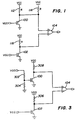
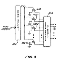
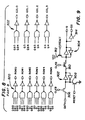
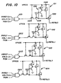
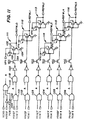
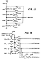
- A memory comprising:characterized by:an array cell (400) having a gate and a floating gate which stores an electrical charge to allow an array threshold value to be programmed;n-1 read reference cells (402-1 to 402-(n-1)), each read reference cell having a gate and a floating gate which stores an electrical charge to allow a read reference threshold value to be programmed;n program reference cells (502-1 to 502 -n), each program reference cell having a gate and a floating gate which stores an electrical charge to allow a program reference threshold value to be programmed;a reference program-verify means (506) for alternately applying program and reference verify voltages to the gates of the n program reference cells to program the n program reference cells to different n program reference threshold values and for alternately applying the program and reference verify voltages to the gates of the n- I read reference cells to program the read reference threshold value for each successive read reference cell between two successive ones of the program reference threshold values;an array program-verify means (504) for alternately applying program and array verify voltages to the gate of the array cell until the array threshold value is programmed to be equal to the program reference threshold value of a given one of the n program reference cells;a selector for supplying a read voltage to the gate of the array cell and the gates of the read reference cells to obtain an array cell output and a read reference cell output from each of the read reference cells; anda comparison means (406) coupled to receive the array cell output and the read reference cell outputs, the comparison means providing a signal indicating the given one of the n program reference cells used to program the array cell.
- The memory of claim 1 wherein the reference verify voltages have values which varies significantly less than the array verify voltages.
- The memory of claim 1 wherein when the read or verify voltages are applied, the read reference cells, the program reference cells and the array cell are biased substantially the same.
- The memory of claim 1 wherein the program reference cells, the read reference cells and the array cell are included as core cells on a single integrated circuit so that the program reference cells, the read reference cells and the array cell have substantially the same rate of thermal expansion.
- The memory of claim 1 wherein when a value of the read voltage is varied a working margin between outputs of the program reference cells, the read reference cell outputs and the array cell output remains constant.
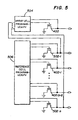
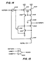
- The memory of claim 1, wherein the reference program-verify means comprises:a golden bit cell having a gate and a drain;a reference bias circuit (610) having a plurality of resistance ratios, each resistance ratio being coupled between a read voltage and the gate of the golden bit cell; anda comparison circuit for receiving the reference verify voltages and being connected to the drain of the golden bit cell and a drain of a particular one of the n program reference and n-1 read reference cells, the comparison circuit comparing the signal from the drain of the golden bit cell to the signal from a drain of the particular reference cell during application of the verify signal and providing an indication when the signals are substantially equal.
- The memory of claim 6 wherein the comparison circuit comprises:a reference sense circuit (612) for receiving the reference verify voltages and outputting a reference sense circuit signal (REFSEN) when the verify signal is applied;a first preamplifier (614) receiving the REFSEN signal, and the signal from the drain of the particular reference cell and outputting a first sense amplifier voltage indicative of the signal from the drain of the particular cell when the REFSEN signal is applied;a second preamplifier receiving the REFSEN signal, and the signal from the drain of the golden bit cell and outputting a second sense amplifier voltage indicative of the signal from the gate of the golden bit cell when the REFSEN signal is applied;a sense amplifier (616) receiving the first and second sense amplifier voltages and outputting a signal indicating when the first and second sense amplifier voltages are substantially equal.
Applications Claiming Priority (2)
| Application Number | Priority Date | Filing Date | Title |
|---|---|---|---|
| US08/160,582 US5828601A (en) | 1993-12-01 | 1993-12-01 | Programmed reference |
| US160582 | 1993-12-01 |
Publications (3)
| Publication Number | Publication Date |
|---|---|
| EP0656628A2 EP0656628A2 (en) | 1995-06-07 |
| EP0656628A3 EP0656628A3 (en) | 1995-08-09 |
| EP0656628B1 true EP0656628B1 (en) | 2003-04-09 |
Family
ID=22577486
Family Applications (1)
| Application Number | Title | Priority Date | Filing Date |
|---|---|---|---|
| EP94308288A Expired - Lifetime EP0656628B1 (en) | 1993-12-01 | 1994-11-10 | Programmed reference |
Country Status (6)
| Country | Link |
|---|---|
| US (1) | US5828601A (en) |
| EP (1) | EP0656628B1 (en) |
| JP (2) | JP3813640B2 (en) |
| KR (1) | KR100357444B1 (en) |
| DE (1) | DE69432452T2 (en) |
| TW (1) | TW302479B (en) |
Cited By (14)
| Publication number | Priority date | Publication date | Assignee | Title |
|---|---|---|---|---|
| US7652930B2 (en) | 2004-04-01 | 2010-01-26 | Saifun Semiconductors Ltd. | Method, circuit and system for erasing one or more non-volatile memory cells |
| US7668017B2 (en) | 2005-08-17 | 2010-02-23 | Saifun Semiconductors Ltd. | Method of erasing non-volatile memory cells |
| US7675782B2 (en) | 2002-10-29 | 2010-03-09 | Saifun Semiconductors Ltd. | Method, system and circuit for programming a non-volatile memory array |
| US7692961B2 (en) | 2006-02-21 | 2010-04-06 | Saifun Semiconductors Ltd. | Method, circuit and device for disturb-control of programming nonvolatile memory cells by hot-hole injection (HHI) and by channel hot-electron (CHE) injection |
| US7701779B2 (en) | 2006-04-27 | 2010-04-20 | Sajfun Semiconductors Ltd. | Method for programming a reference cell |
| US7738304B2 (en) | 2002-07-10 | 2010-06-15 | Saifun Semiconductors Ltd. | Multiple use memory chip |
| US7743230B2 (en) | 2003-01-31 | 2010-06-22 | Saifun Semiconductors Ltd. | Memory array programming circuit and a method for using the circuit |
| US7760554B2 (en) | 2006-02-21 | 2010-07-20 | Saifun Semiconductors Ltd. | NROM non-volatile memory and mode of operation |
| US7786512B2 (en) | 2005-07-18 | 2010-08-31 | Saifun Semiconductors Ltd. | Dense non-volatile memory array and method of fabrication |
| US7808818B2 (en) | 2006-01-12 | 2010-10-05 | Saifun Semiconductors Ltd. | Secondary injection for NROM |
| US7964459B2 (en) | 2004-10-14 | 2011-06-21 | Spansion Israel Ltd. | Non-volatile memory structure and method of fabrication |
| US8053812B2 (en) | 2005-03-17 | 2011-11-08 | Spansion Israel Ltd | Contact in planar NROM technology |
| US8253452B2 (en) | 2006-02-21 | 2012-08-28 | Spansion Israel Ltd | Circuit and method for powering up an integrated circuit and an integrated circuit utilizing same |
| US8400841B2 (en) | 2005-06-15 | 2013-03-19 | Spansion Israel Ltd. | Device to program adjacent storage cells of different NROM cells |
Families Citing this family (57)
| Publication number | Priority date | Publication date | Assignee | Title |
|---|---|---|---|---|
| EP0617363B1 (en) * | 1989-04-13 | 2000-01-26 | SanDisk Corporation | Defective cell substitution in EEprom array |
| US6222762B1 (en) | 1992-01-14 | 2001-04-24 | Sandisk Corporation | Multi-state memory |
| US7071060B1 (en) | 1996-02-28 | 2006-07-04 | Sandisk Corporation | EEPROM with split gate source side infection with sidewall spacers |
| JP3336813B2 (en) * | 1995-02-01 | 2002-10-21 | ソニー株式会社 | Nonvolatile semiconductor memory device |
| FR2745114B1 (en) * | 1996-02-20 | 1998-04-17 | Sgs Thomson Microelectronics | NON-VOLATILE ELECTRICALLY MODIFIABLE MEMORY WITH SELF-CONTAINED COOLING |
| IL125604A (en) | 1997-07-30 | 2004-03-28 | Saifun Semiconductors Ltd | Non-volatile electrically erasable and programmble semiconductor memory cell utilizing asymmetrical charge |
| KR100339023B1 (en) | 1998-03-28 | 2002-09-18 | 주식회사 하이닉스반도체 | Sensing circuit for threshold voltage regulatable flash memory device |
| FR2786910B1 (en) * | 1998-12-04 | 2002-11-29 | St Microelectronics Sa | MULTILEVEL FLOATING GRID MEMORY |
| KR100295361B1 (en) * | 1998-12-30 | 2001-07-12 | 윤종용 | Nonvolatile Semiconductor Memory Devices |
| FR2794277B1 (en) * | 1999-05-25 | 2001-08-10 | St Microelectronics Sa | LOW CONSUMPTION DEAD MEMORY |
| US6215702B1 (en) | 2000-02-16 | 2001-04-10 | Advanced Micro Devices, Inc. | Method of maintaining constant erasing speeds for non-volatile memory cells |
| JP3776307B2 (en) * | 2000-04-26 | 2006-05-17 | 沖電気工業株式会社 | Nonvolatile memory analog voltage writing circuit |
| US6396741B1 (en) | 2000-05-04 | 2002-05-28 | Saifun Semiconductors Ltd. | Programming of nonvolatile memory cells |
| US6490204B2 (en) * | 2000-05-04 | 2002-12-03 | Saifun Semiconductors Ltd. | Programming and erasing methods for a reference cell of an NROM array |
| US6538922B1 (en) | 2000-09-27 | 2003-03-25 | Sandisk Corporation | Writable tracking cells |
| US6449190B1 (en) * | 2001-01-17 | 2002-09-10 | Advanced Micro Devices, Inc. | Adaptive reference cells for a memory device |
| US6538923B1 (en) * | 2001-02-26 | 2003-03-25 | Advanced Micro Devices, Inc. | Staircase program verify for multi-level cell flash memory designs |
| US6466480B2 (en) * | 2001-03-27 | 2002-10-15 | Micron Technology, Inc. | Method and apparatus for trimming non-volatile memory cells |
| US6584017B2 (en) | 2001-04-05 | 2003-06-24 | Saifun Semiconductors Ltd. | Method for programming a reference cell |
| IL148960A (en) * | 2001-04-05 | 2005-09-25 | Saifun Semiconductors Ltd | Method for programming a reference cell |
| TW504702B (en) * | 2001-04-13 | 2002-10-01 | Amic Technology Corp | Circuit and method for correcting overerased flash memory cells |
| US6643169B2 (en) * | 2001-09-18 | 2003-11-04 | Intel Corporation | Variable level memory |
| US6678192B2 (en) | 2001-11-02 | 2004-01-13 | Sandisk Corporation | Error management for writable tracking storage units |
| DE60134870D1 (en) | 2001-12-28 | 2008-08-28 | St Microelectronics Srl | Programming method for a multi-bit memory cell |
| US6975536B2 (en) * | 2002-01-31 | 2005-12-13 | Saifun Semiconductors Ltd. | Mass storage array and methods for operation thereof |
| US6826107B2 (en) | 2002-08-01 | 2004-11-30 | Saifun Semiconductors Ltd. | High voltage insertion in flash memory cards |
| US6963505B2 (en) * | 2002-10-29 | 2005-11-08 | Aifun Semiconductors Ltd. | Method circuit and system for determining a reference voltage |
| US6992932B2 (en) | 2002-10-29 | 2006-01-31 | Saifun Semiconductors Ltd | Method circuit and system for read error detection in a non-volatile memory array |
| US6967896B2 (en) | 2003-01-30 | 2005-11-22 | Saifun Semiconductors Ltd | Address scramble |
| US7142464B2 (en) * | 2003-04-29 | 2006-11-28 | Saifun Semiconductors Ltd. | Apparatus and methods for multi-level sensing in a memory array |
| US7237074B2 (en) * | 2003-06-13 | 2007-06-26 | Sandisk Corporation | Tracking cells for a memory system |
| US6954393B2 (en) * | 2003-09-16 | 2005-10-11 | Saifun Semiconductors Ltd. | Reading array cell with matched reference cell |
| US7123532B2 (en) | 2003-09-16 | 2006-10-17 | Saifun Semiconductors Ltd. | Operating array cells with matched reference cells |
| US7301807B2 (en) | 2003-10-23 | 2007-11-27 | Sandisk Corporation | Writable tracking cells |
| US7755938B2 (en) * | 2004-04-19 | 2010-07-13 | Saifun Semiconductors Ltd. | Method for reading a memory array with neighbor effect cancellation |
| US7095655B2 (en) | 2004-08-12 | 2006-08-22 | Saifun Semiconductors Ltd. | Dynamic matching of signal path and reference path for sensing |
| ITMI20041927A1 (en) * | 2004-10-12 | 2005-01-12 | Atmel Corp | SYSTEM AND METHOD PEE AVOID OFFSET AND REDUCE THE FOOTPRINT OF A NON-VOLATILE MEMORY |
| US7257025B2 (en) * | 2004-12-09 | 2007-08-14 | Saifun Semiconductors Ltd | Method for reading non-volatile memory cells |
| EP1831892A4 (en) * | 2004-12-23 | 2009-06-10 | Atmel Corp | System for performing fast testing during flash reference cell setting |
| US7184313B2 (en) | 2005-06-17 | 2007-02-27 | Saifun Semiconductors Ltd. | Method circuit and system for compensating for temperature induced margin loss in non-volatile memory cells |
| US7221138B2 (en) * | 2005-09-27 | 2007-05-22 | Saifun Semiconductors Ltd | Method and apparatus for measuring charge pump output current |
| JP2007164934A (en) * | 2005-12-16 | 2007-06-28 | Fujitsu Ltd | Nonvolatile semiconductor memory device |
| KR100772389B1 (en) * | 2006-01-12 | 2007-11-01 | 삼성전자주식회사 | Apparatus for cognizing memory |
| US7638835B2 (en) * | 2006-02-28 | 2009-12-29 | Saifun Semiconductors Ltd. | Double density NROM with nitride strips (DDNS) |
| US8848442B2 (en) | 2006-03-06 | 2014-09-30 | Sandisk Il Ltd. | Multi-bit-per-cell flash memory device with non-bijective mapping |
| US7388781B2 (en) * | 2006-03-06 | 2008-06-17 | Sandisk Il Ltd. | Multi-bit-per-cell flash memory device with non-bijective mapping |
| ITMI20062211A1 (en) * | 2006-11-17 | 2008-05-18 | St Microelectronics Srl | CIRCUIT AND METHOD TO GENERATE REFERENCE VOLTAGE IN NON-VOLATILE CELL MEMORY MEMORY DEVICES |
| US7590001B2 (en) | 2007-12-18 | 2009-09-15 | Saifun Semiconductors Ltd. | Flash memory with optimized write sector spares |
| US7778098B2 (en) * | 2007-12-31 | 2010-08-17 | Cypress Semiconductor Corporation | Dummy cell for memory circuits |
| US20090219776A1 (en) | 2008-02-29 | 2009-09-03 | Xian Liu | Non-volatile memory device with plural reference cells, and method of setting the reference cells |
| KR101055568B1 (en) | 2009-06-17 | 2011-08-08 | 한양대학교 산학협력단 | Sensing Circuit of Flash Memory Device and Sensing Method of Flash Memory Device |
| US9424946B2 (en) * | 2013-02-08 | 2016-08-23 | Seagate Technology Llc | Non-volatile buffering to enable sloppy writes and fast write verification |
| KR102111510B1 (en) * | 2014-04-10 | 2020-05-19 | 에스케이하이닉스 주식회사 | Electronic device |
| US11822358B2 (en) * | 2018-08-27 | 2023-11-21 | Sigmasense, Llc. | Drive-sense circuit to determine effects of different electrical characteristics on load |
| US11430516B2 (en) | 2020-04-06 | 2022-08-30 | Crossbar, Inc. | Distinct chip identifier sequence utilizing unclonable characteristics of resistive memory on a chip |
| US11727986B2 (en) * | 2020-04-06 | 2023-08-15 | Crossbar, Inc. | Physically unclonable function (PUF) generation involving programming of marginal bits |
| US11823739B2 (en) * | 2020-04-06 | 2023-11-21 | Crossbar, Inc. | Physically unclonable function (PUF) generation involving high side programming of bits |
Family Cites Families (11)
| Publication number | Priority date | Publication date | Assignee | Title |
|---|---|---|---|---|
| US4449203A (en) * | 1981-02-25 | 1984-05-15 | Motorola, Inc. | Memory with reference voltage generator |
| US4495602A (en) * | 1981-12-28 | 1985-01-22 | Mostek Corporation | Multi-bit read only memory circuit |
| FR2599176A1 (en) * | 1986-05-23 | 1987-11-27 | Eurotechnique Sa | MEMORY DEADLY PROGRAMMABLE ELECTRICALLY |
| JPH02260298A (en) * | 1989-03-31 | 1990-10-23 | Oki Electric Ind Co Ltd | Non-volatile multilevel memory device |
| US5172338B1 (en) * | 1989-04-13 | 1997-07-08 | Sandisk Corp | Multi-state eeprom read and write circuits and techniques |
| EP0477369B1 (en) * | 1989-06-12 | 1997-08-13 | Kabushiki Kaisha Toshiba | Semiconductor memory device |
| JPH0346197A (en) * | 1989-07-13 | 1991-02-27 | Fujitsu Ltd | Semiconductor storage device |
| FR2650109B1 (en) * | 1989-07-20 | 1993-04-02 | Gemplus Card Int | INTEGRATED MOS CIRCUIT WITH ADJUSTABLE THRESHOLD VOLTAGE |
| JP2853217B2 (en) * | 1989-11-21 | 1999-02-03 | 日本電気株式会社 | Semiconductor memory |
| JP3454520B2 (en) * | 1990-11-30 | 2003-10-06 | インテル・コーポレーション | Circuit and method for checking write state of flash storage device |
| US5218569A (en) * | 1991-02-08 | 1993-06-08 | Banks Gerald J | Electrically alterable non-volatile memory with n-bits per memory cell |
-
1993
- 1993-12-01 US US08/160,582 patent/US5828601A/en not_active Expired - Lifetime
-
1994
- 1994-03-10 TW TW083102080A patent/TW302479B/zh not_active IP Right Cessation
- 1994-11-10 DE DE69432452T patent/DE69432452T2/en not_active Expired - Fee Related
- 1994-11-10 EP EP94308288A patent/EP0656628B1/en not_active Expired - Lifetime
- 1994-11-25 KR KR1019940031281A patent/KR100357444B1/en not_active IP Right Cessation
- 1994-11-29 JP JP29465394A patent/JP3813640B2/en not_active Expired - Lifetime
-
2006
- 2006-04-18 JP JP2006114736A patent/JP2006196184A/en active Pending
Cited By (14)
| Publication number | Priority date | Publication date | Assignee | Title |
|---|---|---|---|---|
| US7738304B2 (en) | 2002-07-10 | 2010-06-15 | Saifun Semiconductors Ltd. | Multiple use memory chip |
| US7675782B2 (en) | 2002-10-29 | 2010-03-09 | Saifun Semiconductors Ltd. | Method, system and circuit for programming a non-volatile memory array |
| US7743230B2 (en) | 2003-01-31 | 2010-06-22 | Saifun Semiconductors Ltd. | Memory array programming circuit and a method for using the circuit |
| US7652930B2 (en) | 2004-04-01 | 2010-01-26 | Saifun Semiconductors Ltd. | Method, circuit and system for erasing one or more non-volatile memory cells |
| US7964459B2 (en) | 2004-10-14 | 2011-06-21 | Spansion Israel Ltd. | Non-volatile memory structure and method of fabrication |
| US8053812B2 (en) | 2005-03-17 | 2011-11-08 | Spansion Israel Ltd | Contact in planar NROM technology |
| US8400841B2 (en) | 2005-06-15 | 2013-03-19 | Spansion Israel Ltd. | Device to program adjacent storage cells of different NROM cells |
| US7786512B2 (en) | 2005-07-18 | 2010-08-31 | Saifun Semiconductors Ltd. | Dense non-volatile memory array and method of fabrication |
| US7668017B2 (en) | 2005-08-17 | 2010-02-23 | Saifun Semiconductors Ltd. | Method of erasing non-volatile memory cells |
| US7808818B2 (en) | 2006-01-12 | 2010-10-05 | Saifun Semiconductors Ltd. | Secondary injection for NROM |
| US7760554B2 (en) | 2006-02-21 | 2010-07-20 | Saifun Semiconductors Ltd. | NROM non-volatile memory and mode of operation |
| US8253452B2 (en) | 2006-02-21 | 2012-08-28 | Spansion Israel Ltd | Circuit and method for powering up an integrated circuit and an integrated circuit utilizing same |
| US7692961B2 (en) | 2006-02-21 | 2010-04-06 | Saifun Semiconductors Ltd. | Method, circuit and device for disturb-control of programming nonvolatile memory cells by hot-hole injection (HHI) and by channel hot-electron (CHE) injection |
| US7701779B2 (en) | 2006-04-27 | 2010-04-20 | Sajfun Semiconductors Ltd. | Method for programming a reference cell |
Also Published As
| Publication number | Publication date |
|---|---|
| TW302479B (en) | 1997-04-11 |
| KR100357444B1 (en) | 2003-01-24 |
| JP3813640B2 (en) | 2006-08-23 |
| DE69432452D1 (en) | 2003-05-15 |
| DE69432452T2 (en) | 2004-03-11 |
| EP0656628A2 (en) | 1995-06-07 |
| US5828601A (en) | 1998-10-27 |
| EP0656628A3 (en) | 1995-08-09 |
| JPH07192478A (en) | 1995-07-28 |
| JP2006196184A (en) | 2006-07-27 |
| KR950020743A (en) | 1995-07-24 |
Similar Documents
| Publication | Publication Date | Title |
|---|---|---|
| EP0656628B1 (en) | Programmed reference | |
| JP3652826B2 (en) | Multi-value storage nonvolatile semiconductor memory | |
| EP0756287B1 (en) | A memory sensing circuit employing multi-current mirrors | |
| US5790453A (en) | Apparatus and method for reading state of multistate non-volatile memory cells | |
| US6009040A (en) | Apparatus and methods for controlling sensing time in a memory device | |
| KR0157342B1 (en) | Voltage sensing method of nonvolatile semiconductor memory | |
| US6324094B1 (en) | Apparatus for reading state of multistate non-volatile memory cells | |
| EP1729302B1 (en) | A circuit for retrieving data stored in semiconductor memory cells | |
| US6650570B2 (en) | Non-volatile semiconductor memory | |
| EP0634750B1 (en) | Apparatus and method for reading multi-level data stored in a semiconductor memory | |
| US5163021A (en) | Multi-state EEprom read and write circuits and techniques | |
| US5661685A (en) | Programmable logic device with configurable power supply | |
| EP0907955B1 (en) | A multiple bits-per-cell flash shift register page buffer | |
| US6621745B1 (en) | Row decoder circuit for use in programming a memory device | |
| KR20010032309A (en) | Memory apparatus including programmable non-volatile multi-bit memory cell, and apparatus and method for demarcating memory states of the cell | |
| US5982662A (en) | Semiconductor memory device with improved read characteristics for data having multi values | |
| KR20000035375A (en) | Nonvolatile semiconductor storage device and data writing method thereof | |
| JP2005535062A (en) | Method for setting a reference level for detecting multi-level memory cell states | |
| US7755945B2 (en) | Page buffer and method of programming and reading a memory | |
| KR100938044B1 (en) | Non volatile memory device and multi level cell programming method thereof | |
| JP4007457B2 (en) | Multi-level memory circuit with regulated read voltage | |
| US20090303803A1 (en) | Independent Bi-Directional Margin Control Per Level and Independently Expandable Reference Cell Levels for Voltage Mode Sensing | |
| US6185130B1 (en) | Programmable current source |
Legal Events
| Date | Code | Title | Description |
|---|---|---|---|
| PUAI | Public reference made under article 153(3) epc to a published international application that has entered the european phase |
Free format text: ORIGINAL CODE: 0009012 |
|
| AK | Designated contracting states |
Kind code of ref document: A2 Designated state(s): BE DE DK ES FR GB GR IE IT LU NL PT SE |
|
| PUAL | Search report despatched |
Free format text: ORIGINAL CODE: 0009013 |
|
| AK | Designated contracting states |
Kind code of ref document: A3 Designated state(s): BE DE DK ES FR GB GR IE IT LU NL PT SE |
|
| 17P | Request for examination filed |
Effective date: 19951113 |
|
| 17Q | First examination report despatched |
Effective date: 20000223 |
|
| GRAH | Despatch of communication of intention to grant a patent |
Free format text: ORIGINAL CODE: EPIDOS IGRA |
|
| GRAH | Despatch of communication of intention to grant a patent |
Free format text: ORIGINAL CODE: EPIDOS IGRA |
|
| GRAA | (expected) grant |
Free format text: ORIGINAL CODE: 0009210 |
|
| AK | Designated contracting states |
Designated state(s): BE DE DK ES FR GB GR IE IT LU NL PT SE |
|
| PG25 | Lapsed in a contracting state [announced via postgrant information from national office to epo] |
Ref country code: NL Free format text: LAPSE BECAUSE OF FAILURE TO SUBMIT A TRANSLATION OF THE DESCRIPTION OR TO PAY THE FEE WITHIN THE PRESCRIBED TIME-LIMIT Effective date: 20030409 Ref country code: IT Free format text: LAPSE BECAUSE OF FAILURE TO SUBMIT A TRANSLATION OF THE DESCRIPTION OR TO PAY THE FEE WITHIN THE PRE;WARNING: LAPSES OF ITALIAN PATENTS WITH EFFECTIVE DATE BEFORE 2007 MAY HAVE OCCURRED AT ANY TIME BEFORE 2007. THE CORRECT EFFECTIVE DATE MAY BE DIFFERENT FROM THE ONE RECORDED.SCRIBED TIME-LIMIT Effective date: 20030409 Ref country code: BE Free format text: LAPSE BECAUSE OF FAILURE TO SUBMIT A TRANSLATION OF THE DESCRIPTION OR TO PAY THE FEE WITHIN THE PRESCRIBED TIME-LIMIT Effective date: 20030409 |
|
| REG | Reference to a national code |
Ref country code: GB Ref legal event code: FG4D |
|
| REG | Reference to a national code |
Ref country code: IE Ref legal event code: FG4D |
|
| PG25 | Lapsed in a contracting state [announced via postgrant information from national office to epo] |
Ref country code: SE Free format text: LAPSE BECAUSE OF FAILURE TO SUBMIT A TRANSLATION OF THE DESCRIPTION OR TO PAY THE FEE WITHIN THE PRESCRIBED TIME-LIMIT Effective date: 20030709 Ref country code: PT Free format text: LAPSE BECAUSE OF FAILURE TO SUBMIT A TRANSLATION OF THE DESCRIPTION OR TO PAY THE FEE WITHIN THE PRESCRIBED TIME-LIMIT Effective date: 20030709 Ref country code: GR Free format text: LAPSE BECAUSE OF FAILURE TO SUBMIT A TRANSLATION OF THE DESCRIPTION OR TO PAY THE FEE WITHIN THE PRESCRIBED TIME-LIMIT Effective date: 20030709 Ref country code: DK Free format text: LAPSE BECAUSE OF FAILURE TO SUBMIT A TRANSLATION OF THE DESCRIPTION OR TO PAY THE FEE WITHIN THE PRESCRIBED TIME-LIMIT Effective date: 20030709 |
|
| NLV1 | Nl: lapsed or annulled due to failure to fulfill the requirements of art. 29p and 29m of the patents act | ||
| PG25 | Lapsed in a contracting state [announced via postgrant information from national office to epo] |
Ref country code: ES Free format text: LAPSE BECAUSE OF FAILURE TO SUBMIT A TRANSLATION OF THE DESCRIPTION OR TO PAY THE FEE WITHIN THE PRESCRIBED TIME-LIMIT Effective date: 20031030 |
|
| PG25 | Lapsed in a contracting state [announced via postgrant information from national office to epo] |
Ref country code: LU Free format text: LAPSE BECAUSE OF NON-PAYMENT OF DUE FEES Effective date: 20031110 Ref country code: IE Free format text: LAPSE BECAUSE OF NON-PAYMENT OF DUE FEES Effective date: 20031110 |
|
| ET | Fr: translation filed | ||
| PLBE | No opposition filed within time limit |
Free format text: ORIGINAL CODE: 0009261 |
|
| STAA | Information on the status of an ep patent application or granted ep patent |
Free format text: STATUS: NO OPPOSITION FILED WITHIN TIME LIMIT |
|
| 26N | No opposition filed |
Effective date: 20040112 |
|
| REG | Reference to a national code |
Ref country code: IE Ref legal event code: MM4A |
|
| PGFP | Annual fee paid to national office [announced via postgrant information from national office to epo] |
Ref country code: GB Payment date: 20061004 Year of fee payment: 13 |
|
| PGFP | Annual fee paid to national office [announced via postgrant information from national office to epo] |
Ref country code: FR Payment date: 20061103 Year of fee payment: 13 |
|
| PGFP | Annual fee paid to national office [announced via postgrant information from national office to epo] |
Ref country code: DE Payment date: 20061130 Year of fee payment: 13 |
|
| REG | Reference to a national code |
Ref country code: GB Ref legal event code: 732E |
|
| REG | Reference to a national code |
Ref country code: GB Ref legal event code: 732E |
|
| GBPC | Gb: european patent ceased through non-payment of renewal fee |
Effective date: 20071110 |
|
| PG25 | Lapsed in a contracting state [announced via postgrant information from national office to epo] |
Ref country code: DE Free format text: LAPSE BECAUSE OF NON-PAYMENT OF DUE FEES Effective date: 20080603 |
|
| REG | Reference to a national code |
Ref country code: FR Ref legal event code: ST Effective date: 20080930 |
|
| PG25 | Lapsed in a contracting state [announced via postgrant information from national office to epo] |
Ref country code: GB Free format text: LAPSE BECAUSE OF NON-PAYMENT OF DUE FEES Effective date: 20071110 |
|
| PG25 | Lapsed in a contracting state [announced via postgrant information from national office to epo] |
Ref country code: FR Free format text: LAPSE BECAUSE OF NON-PAYMENT OF DUE FEES Effective date: 20071130 |
|
| REG | Reference to a national code |
Ref country code: GB Ref legal event code: 732E Free format text: REGISTERED BETWEEN 20150618 AND 20150624 |