EP0660140A1 - Method for making a relief structure on a substrate from semiconductor material - Google Patents
Method for making a relief structure on a substrate from semiconductor material Download PDFInfo
- Publication number
- EP0660140A1 EP0660140A1 EP94402969A EP94402969A EP0660140A1 EP 0660140 A1 EP0660140 A1 EP 0660140A1 EP 94402969 A EP94402969 A EP 94402969A EP 94402969 A EP94402969 A EP 94402969A EP 0660140 A1 EP0660140 A1 EP 0660140A1
- Authority
- EP
- European Patent Office
- Prior art keywords
- wafer
- ions
- profile
- implantation
- relief structure
- Prior art date
- Legal status (The legal status is an assumption and is not a legal conclusion. Google has not performed a legal analysis and makes no representation as to the accuracy of the status listed.)
- Granted
Links
Images


Classifications
-
- G—PHYSICS
- G02—OPTICS
- G02B—OPTICAL ELEMENTS, SYSTEMS OR APPARATUS
- G02B5/00—Optical elements other than lenses
- G02B5/18—Diffraction gratings
- G02B5/1876—Diffractive Fresnel lenses; Zone plates; Kinoforms
- G02B5/189—Structurally combined with optical elements not having diffractive power
- G02B5/1895—Structurally combined with optical elements not having diffractive power such optical elements having dioptric power
-
- G—PHYSICS
- G02—OPTICS
- G02B—OPTICAL ELEMENTS, SYSTEMS OR APPARATUS
- G02B5/00—Optical elements other than lenses
- G02B5/18—Diffraction gratings
- G02B5/1847—Manufacturing methods
- G02B5/1857—Manufacturing methods using exposure or etching means, e.g. holography, photolithography, exposure to electron or ion beams
-
- G—PHYSICS
- G02—OPTICS
- G02B—OPTICAL ELEMENTS, SYSTEMS OR APPARATUS
- G02B5/00—Optical elements other than lenses
- G02B5/18—Diffraction gratings
- G02B5/1876—Diffractive Fresnel lenses; Zone plates; Kinoforms
-
- G—PHYSICS
- G02—OPTICS
- G02B—OPTICAL ELEMENTS, SYSTEMS OR APPARATUS
- G02B6/00—Light guides; Structural details of arrangements comprising light guides and other optical elements, e.g. couplings
- G02B6/10—Light guides; Structural details of arrangements comprising light guides and other optical elements, e.g. couplings of the optical waveguide type
- G02B6/12—Light guides; Structural details of arrangements comprising light guides and other optical elements, e.g. couplings of the optical waveguide type of the integrated circuit kind
- G02B6/13—Integrated optical circuits characterised by the manufacturing method
- G02B6/134—Integrated optical circuits characterised by the manufacturing method by substitution by dopant atoms
- G02B6/1347—Integrated optical circuits characterised by the manufacturing method by substitution by dopant atoms using ion implantation
-
- H—ELECTRICITY
- H01—ELECTRIC ELEMENTS
- H01L—SEMICONDUCTOR DEVICES NOT COVERED BY CLASS H10
- H01L21/00—Processes or apparatus adapted for the manufacture or treatment of semiconductor or solid state devices or of parts thereof
- H01L21/02—Manufacture or treatment of semiconductor devices or of parts thereof
- H01L21/04—Manufacture or treatment of semiconductor devices or of parts thereof the devices having at least one potential-jump barrier or surface barrier, e.g. PN junction, depletion layer or carrier concentration layer
- H01L21/18—Manufacture or treatment of semiconductor devices or of parts thereof the devices having at least one potential-jump barrier or surface barrier, e.g. PN junction, depletion layer or carrier concentration layer the devices having semiconductor bodies comprising elements of Group IV of the Periodic System or AIIIBV compounds with or without impurities, e.g. doping materials
- H01L21/185—Joining of semiconductor bodies for junction formation
-
- H—ELECTRICITY
- H01—ELECTRIC ELEMENTS
- H01L—SEMICONDUCTOR DEVICES NOT COVERED BY CLASS H10
- H01L21/00—Processes or apparatus adapted for the manufacture or treatment of semiconductor or solid state devices or of parts thereof
- H01L21/70—Manufacture or treatment of devices consisting of a plurality of solid state components formed in or on a common substrate or of parts thereof; Manufacture of integrated circuit devices or of parts thereof
- H01L21/71—Manufacture of specific parts of devices defined in group H01L21/70
- H01L21/76—Making of isolation regions between components
- H01L21/762—Dielectric regions, e.g. EPIC dielectric isolation, LOCOS; Trench refilling techniques, SOI technology, use of channel stoppers
- H01L21/7624—Dielectric regions, e.g. EPIC dielectric isolation, LOCOS; Trench refilling techniques, SOI technology, use of channel stoppers using semiconductor on insulator [SOI] technology
- H01L21/76251—Dielectric regions, e.g. EPIC dielectric isolation, LOCOS; Trench refilling techniques, SOI technology, use of channel stoppers using semiconductor on insulator [SOI] technology using bonding techniques
- H01L21/76254—Dielectric regions, e.g. EPIC dielectric isolation, LOCOS; Trench refilling techniques, SOI technology, use of channel stoppers using semiconductor on insulator [SOI] technology using bonding techniques with separation/delamination along an ion implanted layer, e.g. Smart-cut, Unibond
-
- Y—GENERAL TAGGING OF NEW TECHNOLOGICAL DEVELOPMENTS; GENERAL TAGGING OF CROSS-SECTIONAL TECHNOLOGIES SPANNING OVER SEVERAL SECTIONS OF THE IPC; TECHNICAL SUBJECTS COVERED BY FORMER USPC CROSS-REFERENCE ART COLLECTIONS [XRACs] AND DIGESTS
- Y10—TECHNICAL SUBJECTS COVERED BY FORMER USPC
- Y10T—TECHNICAL SUBJECTS COVERED BY FORMER US CLASSIFICATION
- Y10T156/00—Adhesive bonding and miscellaneous chemical manufacture
- Y10T156/10—Methods of surface bonding and/or assembly therefor
- Y10T156/1052—Methods of surface bonding and/or assembly therefor with cutting, punching, tearing or severing
Definitions
- the present invention relates to a method for producing a relief structure on a support made of semiconductor material. This method makes it possible in particular to advantageously produce devices for binary optics on a support made of semiconductor material, in particular silicon.
- One of the simplest structures that can be produced in binary optics is the prism which is presented as a series of micro-steps of staircase cut in the surface of the material.
- a wave front arrives at the surface, this wave is separated into secondary wave fronts (according to the Huygens-Fresnel principle).
- Each secondary wavefront is delayed in proportion to the height of the step at this point, that is to say the additional optical path crossed.
- these wave fronts interfere with each other, they produce a new wave front propagating at an angle to the direction of the incident wave front.
- a material thickness of the order of ⁇ m (corresponding to the wavelength ⁇ of an incident light beam) is sufficient to obtain the deflection effect while in conventional approach , a piece of glass several millimeters thick would have been necessary.
- the realization of binary optics therefore requires knowing how to perform locally on the surface of a material of the over-thickness or under-thickness zones (the over-thickness or the under-thickness must be obtained precisely because it corresponds to a fraction of the wavelength of use of the device).
- the location of these areas is dependent on the optical function to be performed.
- the techniques of deposition in a thin layer are used, when it is desired to make an embodiment in relief, associated with lithography and etching techniques for the location of the overlying areas. thickness.
- lithography techniques for localization and engraving (dry for example).
- the result obtained is linked to the reaction kinetics and to the time of application of the reaction.
- the process parameters are set and applied for a period of time.
- document FR-A-2 681 472 discloses a method for manufacturing thin films of semiconductor material comprising three steps.
- a first step a layer of gaseous microbubbles is created by ion implantation under one face of a wafer of semiconductor material.
- the face of the wafer is made integral with a stiffener.
- the assembly consisting of the wafer and the stiffener is subjected to a temperature sufficient to create, by effect of crystal rearrangement in the wafer and pressure in the microbubbles, a cleavage of the wafer at the level of the layer of microbubbles. This gives a thin film adhering to the stiffener.
- the present invention provides a new method for producing a relief structure on a support made of semiconductor material which uses a technique derived from the teaching of document FR-A-2 681 472. This new method thus makes it possible to remedy the disadvantages of manufacturing methods according to known art.
- the zones of gaseous microbubbles of different implantation energies can be obtained by stages successive locations.
- all the zones of gaseous microbubbles can be created simultaneously thanks to a screen arranged on the path of the ions, this screen being able to be crossed by the ions while attenuating their energies and having a thickness varying locally according to a pattern corresponding to the microbubble zones to be created to allow the implantation energy required for each zone to pass.
- the semiconductor may be silicon, the implanted ions of hydrogen gas or helium ions, the implantation temperature between 20 ° C and 400 ° C and the temperature of the third heat treatment step greater than 450 ° C.
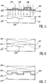
- FIG 1 there is shown a wafer 1 of semiconductor material, for example monocrystalline silicon. This plate is seen from the side. It has an upper planar face 2 through which we will produce by implanting zones of gaseous microbubbles in its volume. We suppose that we want to implant two zones there corresponding to a first energy level of the ions and two zones corresponding to a second energy level of the ions, this second energy level being higher than the first.
- semiconductor material for example monocrystalline silicon
- the ions used for implantation by bombardment are for example H+ ions, but it is also possible to use molecular ions of hydrogen or ions of rare gases such as helium, neon, krypton and xenon, used individually or in combination.
- group IV semiconductors for example silicon, germanium, silicon carbide, silicon-germanium alloys.
- the implantation of ions generally referenced 3 causes, for a given implantation energy, two zones of gas microbubbles 4 and 5 located at the same depth of the flat face 2 of the wafer 1. On can set up each zone 4 or 5 successively or simultaneously by placing a mask on the path of the ion beam.
- the zones 6 and 7 located deeper in the wafer 1 are implanted by higher energy ions generally referenced 8.
- the zones 6 and 7 join zones 4 and 5 if all these zones are projected onto the flat face 2.
- the location of the implantation in well-defined zones can be achieved using known techniques, for example by using an implantation through a resin mask obtained by photolitography or the implantation through a metal mask having openings.
- All of the implanted areas constitute a profile delimiting an upper region 9 and a lower region 10 in the volume of the wafer.
- FIG. 3 shows the semiconductor wafer 1, obtained at the end of the first step, made integral with a stiffener 11 by its flat face 2.
- the stiffener can be fixed to the semiconductor wafer by bonding thanks to a substance adhering to the both to the stiffener and to the insert. But preferably, the stiffener is integral with the wafer via inter-atomic links as described in documents FR-A-2 681 472 or EP-A-0 533 551.
- the stiffener must in any case be able to support the heat treatment of the third step without risking deterioration, while remaining integral with the wafer.
- the heat treatment must be carried out at a temperature such that the crystal rearrangement and the coalescence of the bubbles can effectively take place.
- a temperature above about 450 ° C is necessary for the separation to take place.
- Figure 4 shows the result obtained after the heat treatment.
- the upper 9 and lower 10 regions are now separated by the space 12, at the location of the implanted zones and of the connection zones between these zones.
- the fracture at the connection zones is due to the embrittlement induced between two relatively close cleavage planes.
- Figures 5 to 7 illustrate a second embodiment of the invention which uses a screen.
- the wafer 20 of semiconductor material for example monocrystalline silicon, has an upper planar face 21 through which the implantation will be carried out which will create zones of gaseous microbubbles in its volume.
- the implantation is done by placing on the path of the ions, bearing the general reference 22, a screen 23 capable of being traversed by the ions but whose thickness affects the energy of the ions. The thicker the screen, the more the energy of the ions will be reduced.
- This screen can be made of silicon for example or of SiC.
- the screen 23 comprises, in the example shown in FIG. 5, three different thicknesses: the regions 24, 25 and 26 are of the same thickness, the region 27 is a little thicker and the region 28 still a little thicker. On this screen, the structure that is to be obtained in the plate is produced in relief.
- Ion bombardment for example by H+ ions of selected energy, takes place over the entire surface of the planar face 21, through the screen 23.
- the ions penetrate more or less deeply into the wafer 20, depending of the thickness of the screen crossed. They cause a continuous profile 29 of gaseous microbubbles delimiting an upper region 30 and a lower region 31 in the volume of the wafer.
- This variant is particularly advantageous because, once the screen has been produced, there is no longer any problem of positioning the different zones therebetween. A single installation is enough and the screen can be used several times.
- FIG. 6 represents the second step of the method: a stiffener 32 is secured to the flat face 21 of the wafer 20.
- FIG. 7 shows the result obtained after the heat treatment. The upper 30 and lower 31 regions are now separated by the space 33 at the location of the implanted areas and the connecting areas, fractured as in the first mode described above.
- a relief structure is obtained on the thin film adhering to the stiffener and an inverted relief structure on the rest of the wafer, that is to say on a semiconductor substrate.
- the structures thus obtained may include variations in levels of the order of a few fractions of ⁇ m to a few tens of ⁇ m.
- the structures thus obtained can find an application in the field of binary optics and also serve as a mold for the production of a polymer optical device.
- FIG. 8 illustrates an example of application of the invention. It is a prism for binary optics.
- the prism 40 is cylindrical in shape. Its upper face has a relief structure obtained according to the method of the invention.
- the prism 40 is for example formed by the mass of a substrate after removal of the upper film secured to the stiffener.
- the structure is, in the case shown, consisting of a central blind hole 41 and concentric rings 42, 43 and 44 of different heights.
- Figures 9 and 10 are sectional views which illustrate an application of the invention in a different field from binary optics. It is a question of obtaining a mold for the production of a conventional optical element but of reduced size, for example a polymer lens.
- a relief structure 51 is produced by the method of the invention on a support 50 of semiconductor material, this support being constituted either by a film adhering to a stiffener or by the rest of the semiconductor wafer used.
- the structure 51 consists of an approximation of a bowl 52 to be obtained. The approximation is obtained by a staircase shape given to the structure.
- the final shape of the mold is obtained by using a smoothing deposit 53 of silicon for example (see FIG. 10).
- Another way of doing this consists in making the structure in relief by approaching the profile of the bowl to be obtained but without reaching it, then finely polishing the structure until reaching the desired profile.
- the method of the invention it is possible, for example, to obtain a bowl 40 ⁇ m in diameter for 4 ⁇ m of maximum depth.
- the invention is particularly advantageous for obtaining shallow shapes, that is to say where the h / l ratio is low. Indeed, these forms are difficult to achieve by other techniques.
- the optical element to be produced from such a mold can then be obtained by deposition or pressure application of a layer of polymer on the mold.
Abstract
Description
La présente invention concerne un procédé de réalisation d'une structure en relief sur un support en matériau semiconducteur. Ce procédé permet en particulier de réaliser avantageusement des dispositifs pour l'optique binaire sur un support en matériau semiconducteur, notamment en silicium.The present invention relates to a method for producing a relief structure on a support made of semiconductor material. This method makes it possible in particular to advantageously produce devices for binary optics on a support made of semiconductor material, in particular silicon.
Les principes de base de l'optique binaire sont simples et s'appliquent aussi bien à une optique en réflexion qu'à une optique en réfraction. Ces principes ont été rappelés dans l'article "Binary Optics" de W.B. VELDKAMP et T.J. McHUGH, paru dans la revue Scientific American de Mai 1992.The basic principles of binary optics are simple and apply as well to a reflection optics as to a refraction optics. These principles were recalled in the article "Binary Optics" by W.B. VELDKAMP and T.J. McHUGH, which appeared in the journal Scientific American in May 1992.
Une des structures les plus simples que l'on puisse réaliser en optique binaire est le prisme qui se présente comme une série de micro-marches d'escalier taillées dans la surface du matériau. Quand un front d'onde arrive à la surface, cette onde est séparée en fronts d'ondes secondaires (selon le principe de Huygens-Fresnel). Chaque front d'onde secondaire est retardé en proportion de la hauteur de la marche en ce point c'est-à-dire du supplément de chemin optique traversé. Quand ces fronts d'onde interfèrent entre eux, ils produisent un nouveau front d'onde se propageant avec un certain angle par rapport à la direction du front d'onde incident.One of the simplest structures that can be produced in binary optics is the prism which is presented as a series of micro-steps of staircase cut in the surface of the material. When a wave front arrives at the surface, this wave is separated into secondary wave fronts (according to the Huygens-Fresnel principle). Each secondary wavefront is delayed in proportion to the height of the step at this point, that is to say the additional optical path crossed. When these wave fronts interfere with each other, they produce a new wave front propagating at an angle to the direction of the incident wave front.
Dans l'approche optique binaire, il suffit d'une épaisseur de matériau de l'ordre du µm (correspondant à la longueur d'onde λ d'un faisceau lumineux incident) pour obtenir l'effet de déflexion alors qu'en approche conventionnelle, il aurait fallu une pièce en verre de plusieurs millimètres d'épaisseur.In the binary optical approach, a material thickness of the order of µm (corresponding to the wavelength λ of an incident light beam) is sufficient to obtain the deflection effect while in conventional approach , a piece of glass several millimeters thick would have been necessary.
La réalisation de dispositifs d'optique binaire requiert donc de savoir réaliser localement à la surface d'un matériau des zones en sur-épaisseur ou sous-épaisseur (la sur-épaisseur ou la sous-épaisseur devant être obtenue précisément car correspondant à une fraction de la longueur d'onde d'utilisation du dispositif). La localisation de ces zones est dépendante de la fonction optique à réaliser. Dans une même optique, on peut trouver plusieurs gammes de sur-épaisseurs (ou sous-épaisseurs) par exemple correspondant à des différences de marche de λ/8, λ/4, 3λ/8, λ/2, etc.The realization of binary optics therefore requires knowing how to perform locally on the surface of a material of the over-thickness or under-thickness zones (the over-thickness or the under-thickness must be obtained precisely because it corresponds to a fraction of the wavelength of use of the device). The location of these areas is dependent on the optical function to be performed. In the same perspective, we can find several ranges of over-thicknesses (or under-thicknesses), for example corresponding to differences in path of λ / 8, λ / 4, 3λ / 8, λ / 2, etc.
Classiquement, pour réaliser un tel dispositif d'optique binaire, on utilise les techniques de dépôt en couche mince, lorsque l'on veut faire une réalisation en relief, associée à des techniques de lithographie et de gravure pour la localisation des zones en sur-épaisseur. Lorsque l'on veut faire une réalisation en creux, on utilise les techniques de lithographie pour la localisation et de gravure (sèche par exemple).Conventionally, to produce such a binary optics device, the techniques of deposition in a thin layer are used, when it is desired to make an embodiment in relief, associated with lithography and etching techniques for the location of the overlying areas. thickness. When we want to make a hollow production, we use lithography techniques for localization and engraving (dry for example).
Ces procédés de fabrication selon l'art connu présentent des inconvénients relatifs au contrôle et à la reproductibilité des épaisseurs des zones, et relatifs également à la complexité des opérations nécessaires pour réaliser plusieurs gammes d'épaisseurs.These manufacturing methods according to the known art have drawbacks relating to the control and reproducibility of the thicknesses of the zones, and also relating to the complexity of the operations necessary to produce several ranges of thicknesses.
En ce qui concerne le contrôle et la reproductibilité des épaisseurs, le résultat obtenu est lié à une cinétique de réaction et au temps d'application de la réaction. Généralement, on règle les paramètres du procédé et on l'applique pendant une durée prévue. On n'a en général pas d'indicateur, pendant l'application du procédé, de l'épaisseur (ou profondeur) courante réalisée. L'incertitude sur le résultat peut être grande.As regards the control and the reproducibility of the thicknesses, the result obtained is linked to the reaction kinetics and to the time of application of the reaction. Generally, the process parameters are set and applied for a period of time. In general, there is no indicator, during the application of the method, of the current thickness (or depth) achieved. Uncertainty about the outcome can be great.
Pour réaliser plusieurs gammes d'épaisseurs, on constate que, quand le procédé est appliqué pour réaliser une gamme d'épaisseur dans une zone donnée, les autres zones doivent être protégées de l'application du procédé. Ceci induit une complexité au niveau de la lithographie ainsi que des problèmes de frontière entre zones dues à des alignements imparfaits.To achieve several ranges of thicknesses, it can be seen that, when the method is applied to achieve a range of thicknesses in a given area, the other zones must be protected from the application of the process. This induces complexity at the lithography level as well as border problems between areas due to imperfect alignments.
On connaît d'autre part, par le document FR-A-2 681 472, un procédé de fabrication de films minces de matériau semiconducteur comprenant trois étapes. Dans une première étape, on crée par implantation ionique une couche de microbulles gazeuses sous une face d'une plaquette de matériau semiconducteur. Dans une seconde étape, la face de la plaquette est rendue solidaire d'un raidisseur. Dans une troisième étape, l'ensemble constitué par la plaquette et le raidisseur est soumis à une température suffisante pour créer, par effet de réarrangement cristallin dans la plaquette et de pression dans les microbulles, un clivage de la plaquette au niveau de la couche de microbulles. On obtient ainsi un film mince adhérant au raidisseur.On the other hand, document FR-A-2 681 472 discloses a method for manufacturing thin films of semiconductor material comprising three steps. In a first step, a layer of gaseous microbubbles is created by ion implantation under one face of a wafer of semiconductor material. In a second step, the face of the wafer is made integral with a stiffener. In a third step, the assembly consisting of the wafer and the stiffener is subjected to a temperature sufficient to create, by effect of crystal rearrangement in the wafer and pressure in the microbubbles, a cleavage of the wafer at the level of the layer of microbubbles. This gives a thin film adhering to the stiffener.
La présente invention propose un nouveau procédé de réalisation d'une structure en relief sur un support en matériau semiconducteur qui met en oeuvre une technique dérivée de l'enseignement du document FR-A-2 681 472. Ce nouveau procédé permet ainsi de remédier aux inconvénients des procédés de fabrication selon l'art connu.The present invention provides a new method for producing a relief structure on a support made of semiconductor material which uses a technique derived from the teaching of document FR-A-2 681 472. This new method thus makes it possible to remedy the disadvantages of manufacturing methods according to known art.
L'invention a donc pour objet un procédé de réalisation d'une structure en relief sur un support en matériau semiconducteur, caractérisé en ce qu'il consiste à soumettre une plaquette de ce matériau semiconducteur comportant une face plane dont le plan est soit sensiblement parallèle à un plan cristallographique principal dans le cas où le matériau semiconducteur est monocristallin, soit faiblement incliné par rapport à un plan cristallographique de mêmes indices pour tous les grains dans le cas où le matériau est polycristallin, aux trois étapes suivantes :
- une première étape d'implantation par bombardement de la face plane de ladite plaquette au moyen d'ions, créant des zones de microbulles gazeuses, l'ensemble des zones définissant un profil dans le volume de ladite plaquette, chaque zone étant située par rapport à ladite face plane à une profondeur dépendant de l'énergie d'implantation des ions reçue par la surface de la face en regard de cette zone et étant de même géométrie que cette surface, ce profil délimitant, du côté de la face plane, une région supérieure de la plaquette constituant un film mince et, du côté opposé à la face plane, une région inférieure constituant la masse du substrat, les ions étant choisis parmi les ions de gaz rares ou de gaz hydrogène et la température de la plaquette pendant l'implantation étant maintenue au-dessous de la température à laquelle le gaz engendré par les ions implantés peut s'échapper du semiconducteur par diffusion ;
- une deuxième étape de solidarisation de la face plane de ladite plaquette avec un raidisseur constitué d'au moins une couche de matériau rigide ;
- une troisième étape de traitement thermique de l'ensemble constitué par la plaquette et le raidisseur à une température suffisante pour créer une séparation entre le film mince et la masse du substrat le long dudit profil, la séparation procurant une structure en relief sur le film mince et une structure en relief inversé sur le substrat.
- a first step of implantation by bombardment of the planar face of said wafer by means of ions, creating zones of gaseous microbubbles, all of the zones defining a profile in the volume of said wafer, each zone being situated relative to said plane face at a depth depending on the implantation energy of the ions received by the surface of the face opposite this zone and being of the same geometry as this surface, this profile delimiting, on the side of the plane face, a region upper part of the wafer constituting a thin film and, on the side opposite to the planar face, a lower region constituting the mass of the substrate, the ions being chosen from ions of rare gas or hydrogen gas and the temperature of the wafer during implantation being maintained below the temperature at which the gas generated by the implanted ions can escape from the semiconductor by diffusion;
- a second step of joining the flat face of said wafer with a stiffener made up of at least one layer of rigid material;
- a third stage of heat treatment of the assembly constituted by the wafer and the stiffener at a temperature sufficient to create a separation between the thin film and the mass of the substrate along said profile, the separation providing a relief structure on the thin film and an inverted relief structure on the substrate.
Lors de la première étape, les zones de microbulles gazeuses d'énergies d'implantation différentes peuvent être obtenues par des étapes d'implantation successives.During the first stage, the zones of gaseous microbubbles of different implantation energies can be obtained by stages successive locations.
Lors de la première étape, toutes les zones de microbulles gazeuses peuvent être créées simultanément grâce à un écran disposé sur le trajet des ions, cet écran étant apte à être traversé par les ions tout en atténuant leurs énergies et ayant une épaisseur variant localement selon un motif correspondant aux zones de microbulles à créer pour laisser passer l'énergie d'implantation nécessaire pour chaque zone.During the first step, all the zones of gaseous microbubbles can be created simultaneously thanks to a screen arranged on the path of the ions, this screen being able to be crossed by the ions while attenuating their energies and having a thickness varying locally according to a pattern corresponding to the microbubble zones to be created to allow the implantation energy required for each zone to pass.
En vue d'obtenir un profil de structure déterminé, on peut réaliser d'abord une structure en relief approchant par excès ledit profil déterminé, puis procéder à une quatrième étape consistant à polir la structure approchante jusqu'à atteindre le profil déterminé.With a view to obtaining a determined structure profile, it is possible first of all to produce a relief structure approaching said determined profile by excess, then to carry out a fourth step consisting in polishing the approaching structure until reaching the determined profile.
En vue d'obtenir un profil de structure déterminé, on peut réaliser d'abord une structure en relief approchant par défaut ledit profil déterminé, puis procéder à une quatrième étape consistant à combler la structure approchante jusqu'à atteindre le profil déterminé.In order to obtain a determined structure profile, it is possible first to produce a relief structure approaching by default said determined profile, then proceed to a fourth step consisting in filling the approaching structure until reaching the determined profile.
Le semiconducteur peut être du silicium, les ions implantés des ions de gaz hydrogène ou d'hélium, la température d'implantation comprise entre 20°C et 400°C et la température de la troisième étape de traitement thermique supérieure à 450°C.The semiconductor may be silicon, the implanted ions of hydrogen gas or helium ions, the implantation temperature between 20 ° C and 400 ° C and the temperature of the third heat treatment step greater than 450 ° C.
L'invention sera mieux comprise et d'autres avantages et particularités apparaîtront à la lecture de la description qui va suivre, donnée à titre d'exemple non limitatif, accompagnée des dessins annexés parmi lesquels :
- les figures 1 à 4 illustrent un premier mode d'application du procédé de réalisation d'une structure en relief selon l'invention,
- les figures 5 à 7 illustrent un deuxième mode d'application du procédé de réalisation d'une structure en relief selon l'invention,
- la figure 8 représente une vue partielle en perspective d'un dispositif d'optique binaire réalisé par le procédé selon l'invention,
- les figures 9 et 10 illustrent une autre réalisation obtenue par le procédé selon l'invention.
- FIGS. 1 to 4 illustrate a first mode of application of the method for producing a relief structure according to the invention,
- FIGS. 5 to 7 illustrate a second mode of application of the method for producing a relief structure according to the invention,
- FIG. 8 represents a partial perspective view of a binary optical device produced by the method according to the invention,
- Figures 9 and 10 illustrate another embodiment obtained by the method according to the invention.
A la figure 1, on a représenté une plaquette 1 en matériau semiconducteur par exemple en silicium monocristallin. Cette plaquette est vue de côté. Elle comporte une face plane supérieure 2 à travers laquelle on va réaliser par implantation des zones de microbulles gazeuses dans son volume. On suppose qu'on veuille y implanter deux zones correspondant à un premier niveau d'énergie des ions et deux zones correspondant à un deuxième niveau d'énergie des ions, ce deuxième niveau d'énergie étant plus élevé que le premier.In Figure 1, there is shown a
Les ions utilisés pour l'implantation par bombardement sont par exemple des ions H⁺, mais on peut également utiliser des ions moléculaires d'hydrogène ou des ions de gaz rares tels que l'hélium, le néon, le krypton et le xénon, utilisés isolément ou en combinaison. L'objet de la présente invention s'applique particulièrement bien aux semiconducteurs du groupe IV, par exemple le silicium, le germanium, le carbure de silicium, les alliages silicium-germanium.The ions used for implantation by bombardment are for example H⁺ ions, but it is also possible to use molecular ions of hydrogen or ions of rare gases such as helium, neon, krypton and xenon, used individually or in combination. The object of the present invention applies particularly well to group IV semiconductors, for example silicon, germanium, silicon carbide, silicon-germanium alloys.
On trouvera dans le document FR-A-2 681 472, déjà cité, des explications concernant l'implantation d'ions H⁺ dans une plaquette de silicium monocristallin.Document FR-A-2 681 472, already cited, contains explanations concerning the implantation of H⁺ ions in a monocrystalline silicon wafer.
Sur la figure 1, l'implantation d'ions référencés de manière générale 3 provoque, pour une énergie d'implantation donnée, deux zones de microbulles gazeuses 4 et 5 situées à une même profondeur de la face plane 2 de la plaquette 1. On peut implanter chaque zone 4 ou 5 successivement ou simultanément en disposant un masque sur le parcours du faisceau d'ions.In FIG. 1, the implantation of ions generally referenced 3 causes, for a given implantation energy, two zones of
De la même façon, comme cela est illustré à la figure 2, on implante les zones 6 et 7 situées plus profondément dans la plaquette 1, par des ions d'énergie supérieure référencés de manière générale 8. Dans le cas présent, les zones 6 et 7 rejoignent les zones 4 et 5 si on projette toutes ces zones sur la face plane 2.In the same way, as illustrated in FIG. 2, the
La localisation de l'implantation à des zones bien déterminées peut être réalisée grâce à des techniques connues, par exemple en utilisant une implantation au travers d'un masque de résine obtenu par photolitographie ou l'implantation au travers d'un masque métallique présentant des ouvertures.The location of the implantation in well-defined zones can be achieved using known techniques, for example by using an implantation through a resin mask obtained by photolitography or the implantation through a metal mask having openings.
L'ensemble des zones implantées constitue un profil délimitant une région supérieure 9 et une région inférieure 10 dans le volume de la plaquette.All of the implanted areas constitute a profile delimiting an
La figure 3 montre la plaquette semiconductrice 1, obtenue à l'issue de la première étape, rendue solidaire d'un raidisseur 11 par sa face plane 2. Le raidisseur peut être fixé à la plaquette semiconductrice par collage grâce à une substance adhérant à la fois au raidisseur et à la plaquette. Mais de façon préférentielle, le raidisseur est solidaire de la plaquette par l'intermédiaire de liaisons inter-atomiques comme décrit dans les documents FR-A-2 681 472 ou EP-A-0 533 551. Le raidisseur doit en tout cas pouvoir supporter le traitement thermique de la troisième étape sans risquer de se dégrader, tout en restant solidaire de la plaquette.FIG. 3 shows the
Le traitement thermique doit être réalisé à une température telle que le réarrangement cristallin et la coalescence des bulles puissent effectivement avoir lieu. Dans le cas d'une plaquette en silicium, une température supérieure à environ 450°C est nécessaire pour que la séparation puisse avoir lieu.The heat treatment must be carried out at a temperature such that the crystal rearrangement and the coalescence of the bubbles can effectively take place. In the case of a silicon wafer, a temperature above about 450 ° C is necessary for the separation to take place.
La figure 4 montre le résultat obtenu après le traitement thermique. Les régions supérieure 9 et inférieure 10 sont maintenant séparées par l'espace 12, à l'endroit des zones implantées et des zones de liaison entre ces zones. La fracture aux zones de liaison est due à la fragilisation induite entre deux plans de clivage relativement proches.Figure 4 shows the result obtained after the heat treatment. The upper 9 and lower 10 regions are now separated by the
Les figures 5 à 7 illustrent un deuxième mode de réalisation de l'invention qui utilise un écran.Figures 5 to 7 illustrate a second embodiment of the invention which uses a screen.
La plaquette 20 en matériau semiconducteur, par exemple en silicium monocristallin, comporte une face plane supérieure 21 à travers laquelle on va réaliser l'implantation qui va créer des zones de microbulles gazeuses dans son volume. L'implantation se fait en plaçant sur le trajet des ions, portant la référence générale 22, un écran 23 apte à être traversé par les ions mais dont l'épaisseur affecte l'énergie des ions. Plus l'écran est épais, plus l'énergie des ions sera réduite. Cet écran peut être réalisé en silicium par exemple ou en SiC.The
L'écran 23 comporte, dans l'exemple représenté à la figure 5, trois épaisseurs différentes : les régions 24, 25 et 26 sont de même épaisseur, la région 27 est un peu plus épaisse et la région 28 encore un peu plus épaisse. Sur cet écran est réalisé en relief la structure que l'on veut obtenir dans la plaquette.The
Le bombardement ionique, par exemple par des ions H⁺ d'énergie choisie, se fait sur toute la surface de la face plane 21, au travers de l'écran 23. Les ions pénètrent plus ou moins profondément dans la plaquette 20, en fonction de l'épaisseur de l'écran traversée. Ils provoquent un profil continu 29 de microbulles gazeuses délimitant une région supérieure 30 et une région inférieure 31 dans le volume de la plaquette.Ion bombardment, for example by H⁺ ions of selected energy, takes place over the entire surface of the
Cette variante de réalisation est particulièrement intéressante car, une fois l'écran réalisé, il n'y a plus de problème de positionnement des différentes zones entre elles. Une seule implantation suffit et l'écran peut être utilisé plusieurs fois.This variant is particularly advantageous because, once the screen has been produced, there is no longer any problem of positioning the different zones therebetween. A single installation is enough and the screen can be used several times.
La suite des étapes est identique au premier mode d'application du procédé. La figure 6 représente la deuxième étape du procédé : un raidisseur 32 est solidarisé sur la face plane 21 de la plaquette 20. La figure 7 montre le résultat obtenu après le traitement thermique. Les régions supérieure 30 et inférieure 31 sont maintenant séparées par l'espace 33 à l'endroit des zones implantées et des zones de liaison, fracturées comme dans le premier mode décrit précédemment.The following steps are identical to the first mode of application of the method. FIG. 6 represents the second step of the method: a
On obtient finalement une structure en relief sur le film mince adhérant au raidisseur et une structure de relief inversé sur le reste de la plaquette, c'est-à-dire sur un substrat semiconducteur.Finally, a relief structure is obtained on the thin film adhering to the stiffener and an inverted relief structure on the rest of the wafer, that is to say on a semiconductor substrate.
Les structures ainsi obtenues peuvent comporter des variations de niveaux de l'ordre de quelques fractions de µm à quelques dizaines de µm. Les structures ainsi obtenues peuvent trouver une application dans le domaine de l'optique binaire et également servir de moule pour la réalisation d'un dispositif d'optique en polymère.The structures thus obtained may include variations in levels of the order of a few fractions of μm to a few tens of μm. The structures thus obtained can find an application in the field of binary optics and also serve as a mold for the production of a polymer optical device.
La figure 8 illustre un exemple d'application de l'invention. Il s'agit d'un prisme pour l'optique binaire. Le prisme 40 est de forme cylindrique. Sa face supérieure possède une structure en relief obtenue selon le procédé de l'invention. Le prisme 40 est par exemple constitué par la masse d'un substrat après enlèvement du film supérieur solidarisé au raidisseur. La structure est, dans le cas représenté, constituée d'un trou borgne central 41 et d'anneaux concentriques 42, 43 et 44 de hauteurs différentes.FIG. 8 illustrates an example of application of the invention. It is a prism for binary optics. The
Les figures 9 et 10 sont des vues en coupe qui illustrent une application de l'invention dans un domaine différent de l'optique binaire. Il s'agit d'obtenir un moule pour la réalisation d'un élément d'optique classique mais de taille réduite, par exemple une lentille en polymère.Figures 9 and 10 are sectional views which illustrate an application of the invention in a different field from binary optics. It is a question of obtaining a mold for the production of a conventional optical element but of reduced size, for example a polymer lens.
On réalise, par le procédé de l'invention, une structure en relief 51 sur un support 50 en matériau semiconducteur, ce support étant constitué soit par un film adhérant à un raidisseur soit par le reste de la plaquette de semiconducteur utilisé. La structure 51 consiste en une approximation d'une cuvette 52 à obtenir. L'approximation est obtenue par une forme en escalier donnée à la structure.A
La forme finale du moule est obtenue par utilisation d'un dépôt lissant 53 de silicium par exemple (voir la figure 10).The final shape of the mold is obtained by using a smoothing
Une autre façon de faire consiste à réaliser la structure en relief en approchant le profil de la cuvette à obtenir mais sans l'atteindre, puis à polir finement la structure jusqu'à atteindre le profil voulu.Another way of doing this consists in making the structure in relief by approaching the profile of the bowl to be obtained but without reaching it, then finely polishing the structure until reaching the desired profile.
Par le procédé de l'invention, on peut obtenir par exemple une cuvette de 40 µm de diamètre pour 4 µm de profondeur maximale. L'invention est particulièrement intéressante pour obtenir des formes peu profondes, c'est-à-dire où le rapport h/l est faible. En effet, ces formes sont difficiles à réaliser par d'autres techniques.By the method of the invention, it is possible, for example, to obtain a
L'élément optique à élaborer à partir d'un tel moule peut être alors obtenu par dépôt ou application sous pression d'une couche de polymère sur le moule.The optical element to be produced from such a mold can then be obtained by deposition or pressure application of a layer of polymer on the mold.
Claims (10)
Applications Claiming Priority (2)
| Application Number | Priority Date | Filing Date | Title |
|---|---|---|---|
| FR9315563A FR2714524B1 (en) | 1993-12-23 | 1993-12-23 | PROCESS FOR MAKING A RELIEF STRUCTURE ON A SUPPORT IN SEMICONDUCTOR MATERIAL |
| FR9315563 | 1993-12-23 |
Publications (2)
| Publication Number | Publication Date |
|---|---|
| EP0660140A1 true EP0660140A1 (en) | 1995-06-28 |
| EP0660140B1 EP0660140B1 (en) | 2000-03-08 |
Family
ID=9454325
Family Applications (1)
| Application Number | Title | Priority Date | Filing Date |
|---|---|---|---|
| EP94402969A Expired - Lifetime EP0660140B1 (en) | 1993-12-23 | 1994-12-21 | Method for making a relief structure on a substrate from semiconductor material |
Country Status (5)
| Country | Link |
|---|---|
| US (1) | US5494835A (en) |
| EP (1) | EP0660140B1 (en) |
| JP (1) | JP3735880B2 (en) |
| DE (1) | DE69423309T2 (en) |
| FR (1) | FR2714524B1 (en) |
Cited By (17)
| Publication number | Priority date | Publication date | Assignee | Title |
|---|---|---|---|---|
| EP0801419A1 (en) * | 1996-04-11 | 1997-10-15 | Commissariat A L'energie Atomique | Process of making a thin semiconductor film comprising electronic devices |
| WO1998033209A1 (en) * | 1997-01-27 | 1998-07-30 | Commissariat A L'energie Atomique | Method for obtaining a thin film, in particular semiconductor, comprising a protected ion zone and involving an ion implantation |
| EP0889505A1 (en) * | 1997-07-03 | 1999-01-07 | STMicroelectronics S.r.l. | Process for cutting trenches in a single crystal substrate |
| US5985742A (en) | 1997-05-12 | 1999-11-16 | Silicon Genesis Corporation | Controlled cleavage process and device for patterned films |
| US6027988A (en) * | 1997-05-28 | 2000-02-22 | The Regents Of The University Of California | Method of separating films from bulk substrates by plasma immersion ion implantation |
| US6225192B1 (en) | 1996-05-15 | 2001-05-01 | Commissariat A L'energie Atomique | Method of producing a thin layer of semiconductor material |
| EP1744365A2 (en) * | 1996-08-27 | 2007-01-17 | Seiko Epson Corporation | Exfoliating method, transferring method of thin film device, and thin film device, thin film integrated circuit device, and liquid crystal display device produced by the same |
| WO2010059367A3 (en) * | 2008-10-30 | 2010-08-05 | Corning Incorporated | Methods and apparatus for producing semiconductor on insulator structures using directed exfoliation |
| US7816225B2 (en) | 2008-10-30 | 2010-10-19 | Corning Incorporated | Methods and apparatus for producing semiconductor on insulator structures using directed exfoliation |
| US8048766B2 (en) | 2003-06-24 | 2011-11-01 | Commissariat A L'energie Atomique | Integrated circuit on high performance chip |
| US8252663B2 (en) | 2009-06-18 | 2012-08-28 | Commissariat A L'energie Atomique Et Aux Energies Alternatives | Method of transferring a thin layer onto a target substrate having a coefficient of thermal expansion different from that of the thin layer |
| US8309431B2 (en) | 2003-10-28 | 2012-11-13 | Commissariat A L'energie Atomique | Method for self-supported transfer of a fine layer by pulsation after implantation or co-implantation |
| US8389379B2 (en) | 2002-12-09 | 2013-03-05 | Commissariat A L'energie Atomique | Method for making a stressed structure designed to be dissociated |
| US8470712B2 (en) | 1997-12-30 | 2013-06-25 | Commissariat A L'energie Atomique | Process for the transfer of a thin film comprising an inclusion creation step |
| US8993410B2 (en) | 2006-09-08 | 2015-03-31 | Silicon Genesis Corporation | Substrate cleaving under controlled stress conditions |
| US9362439B2 (en) | 2008-05-07 | 2016-06-07 | Silicon Genesis Corporation | Layer transfer of films utilizing controlled shear region |
| EP0994503B1 (en) * | 1998-10-16 | 2016-08-24 | Commissariat à l'Énergie Atomique et aux Énergies Alternatives | Process for manufacturing a structure comprising a thin layer composed of material containing conductive and isolation regions |
Families Citing this family (70)
| Publication number | Priority date | Publication date | Assignee | Title |
|---|---|---|---|---|
| FR2715501B1 (en) * | 1994-01-26 | 1996-04-05 | Commissariat Energie Atomique | Method for depositing semiconductor wafers on a support. |
| FR2738671B1 (en) * | 1995-09-13 | 1997-10-10 | Commissariat Energie Atomique | PROCESS FOR PRODUCING THIN FILMS WITH SEMICONDUCTOR MATERIAL |
| FR2748850B1 (en) | 1996-05-15 | 1998-07-24 | Commissariat Energie Atomique | PROCESS FOR MAKING A THIN FILM OF SOLID MATERIAL AND APPLICATIONS OF THIS PROCESS |
| FR2755537B1 (en) * | 1996-11-05 | 1999-03-05 | Commissariat Energie Atomique | METHOD FOR MANUFACTURING A THIN FILM ON A SUPPORT AND STRUCTURE THUS OBTAINED |
| KR100232886B1 (en) * | 1996-11-23 | 1999-12-01 | 김영환 | Soi wafer fabricating method |
| FR2756847B1 (en) * | 1996-12-09 | 1999-01-08 | Commissariat Energie Atomique | METHOD FOR SEPARATING AT LEAST TWO ELEMENTS OF A STRUCTURE IN CONTACT WITH THEM BY ION IMPLANTATION |
| US6191007B1 (en) | 1997-04-28 | 2001-02-20 | Denso Corporation | Method for manufacturing a semiconductor substrate |
| US6251754B1 (en) | 1997-05-09 | 2001-06-26 | Denso Corporation | Semiconductor substrate manufacturing method |
| US20070122997A1 (en) | 1998-02-19 | 2007-05-31 | Silicon Genesis Corporation | Controlled process and resulting device |
| US6291313B1 (en) | 1997-05-12 | 2001-09-18 | Silicon Genesis Corporation | Method and device for controlled cleaving process |
| US6582999B2 (en) * | 1997-05-12 | 2003-06-24 | Silicon Genesis Corporation | Controlled cleavage process using pressurized fluid |
| US6033974A (en) * | 1997-05-12 | 2000-03-07 | Silicon Genesis Corporation | Method for controlled cleaving process |
| US5877070A (en) * | 1997-05-31 | 1999-03-02 | Max-Planck Society | Method for the transfer of thin layers of monocrystalline material to a desirable substrate |
| US5949108A (en) * | 1997-06-30 | 1999-09-07 | Intel Corporation | Semiconductor device with reduced capacitance |
| US6548382B1 (en) * | 1997-07-18 | 2003-04-15 | Silicon Genesis Corporation | Gettering technique for wafers made using a controlled cleaving process |
| US6534380B1 (en) * | 1997-07-18 | 2003-03-18 | Denso Corporation | Semiconductor substrate and method of manufacturing the same |
| FR2766620B1 (en) | 1997-07-22 | 2000-12-01 | Commissariat Energie Atomique | PRODUCTION OF MICROSTRUCTURES OR NANOSTRUCTURES ON A SUPPORT |
| FR2767416B1 (en) | 1997-08-12 | 1999-10-01 | Commissariat Energie Atomique | PROCESS FOR PRODUCING A THIN FILM OF SOLID MATERIAL |
| US5933750A (en) * | 1998-04-03 | 1999-08-03 | Motorola, Inc. | Method of fabricating a semiconductor device with a thinned substrate |
| US5909627A (en) * | 1998-05-18 | 1999-06-01 | Philips Electronics North America Corporation | Process for production of thin layers of semiconductor material |
| US6291326B1 (en) | 1998-06-23 | 2001-09-18 | Silicon Genesis Corporation | Pre-semiconductor process implant and post-process film separation |
| US6054370A (en) * | 1998-06-30 | 2000-04-25 | Intel Corporation | Method of delaminating a pre-fabricated transistor layer from a substrate for placement on another wafer |
| US6346458B1 (en) * | 1998-12-31 | 2002-02-12 | Robert W. Bower | Transposed split of ion cut materials |
| US20040229443A1 (en) * | 1998-12-31 | 2004-11-18 | Bower Robert W. | Structures, materials and methods for fabrication of nanostructures by transposed split of ion cut materials |
| US20050124142A1 (en) * | 1998-12-31 | 2005-06-09 | Bower Robert W. | Transposed split of ion cut materials |
| US6287941B1 (en) | 1999-04-21 | 2001-09-11 | Silicon Genesis Corporation | Surface finishing of SOI substrates using an EPI process |
| US6204151B1 (en) | 1999-04-21 | 2001-03-20 | Silicon Genesis Corporation | Smoothing method for cleaved films made using thermal treatment |
| US6171965B1 (en) | 1999-04-21 | 2001-01-09 | Silicon Genesis Corporation | Treatment method of cleaved film for the manufacture of substrates |
| US6881644B2 (en) * | 1999-04-21 | 2005-04-19 | Silicon Genesis Corporation | Smoothing method for cleaved films made using a release layer |
| JP2003506883A (en) * | 1999-08-10 | 2003-02-18 | シリコン ジェネシス コーポレイション | Cleavage process for manufacturing multi-layer substrates with low implant dose |
| US6221740B1 (en) | 1999-08-10 | 2001-04-24 | Silicon Genesis Corporation | Substrate cleaving tool and method |
| US6500732B1 (en) | 1999-08-10 | 2002-12-31 | Silicon Genesis Corporation | Cleaving process to fabricate multilayered substrates using low implantation doses |
| US6263941B1 (en) | 1999-08-10 | 2001-07-24 | Silicon Genesis Corporation | Nozzle for cleaving substrates |
| FR2809867B1 (en) * | 2000-05-30 | 2003-10-24 | Commissariat Energie Atomique | FRAGILE SUBSTRATE AND METHOD FOR MANUFACTURING SUCH SUBSTRATE |
| US6303469B1 (en) | 2000-06-07 | 2001-10-16 | Micron Technology, Inc. | Thin microelectronic substrates and methods of manufacture |
| JP2002124652A (en) * | 2000-10-16 | 2002-04-26 | Seiko Epson Corp | Manufacturing method of semiconductor substrate, the semiconductor substrate, electro-optical device, and electronic appliance |
| FR2835096B1 (en) * | 2002-01-22 | 2005-02-18 | PROCESS FOR MANUFACTURING SELF-CARRIER SUBSTRATE OF SINGLE-CRYSTALLINE SEMICONDUCTOR MATERIAL | |
| US7407869B2 (en) * | 2000-11-27 | 2008-08-05 | S.O.I.Tec Silicon On Insulator Technologies | Method for manufacturing a free-standing substrate made of monocrystalline semiconductor material |
| US7094667B1 (en) | 2000-12-28 | 2006-08-22 | Bower Robert W | Smooth thin film layers produced by low temperature hydrogen ion cut |
| FR2823599B1 (en) | 2001-04-13 | 2004-12-17 | Commissariat Energie Atomique | DEMOMTABLE SUBSTRATE WITH CONTROLLED MECHANICAL HOLDING AND METHOD OF MAKING |
| JP2004063730A (en) * | 2002-07-29 | 2004-02-26 | Shin Etsu Handotai Co Ltd | Manufacturing method for soi wafer |
| US7508034B2 (en) * | 2002-09-25 | 2009-03-24 | Sharp Kabushiki Kaisha | Single-crystal silicon substrate, SOI substrate, semiconductor device, display device, and manufacturing method of semiconductor device |
| JP2004119943A (en) * | 2002-09-30 | 2004-04-15 | Renesas Technology Corp | Semiconductor wafer and manufacturing method therefor |
| US8187377B2 (en) | 2002-10-04 | 2012-05-29 | Silicon Genesis Corporation | Non-contact etch annealing of strained layers |
| FR2857953B1 (en) | 2003-07-21 | 2006-01-13 | Commissariat Energie Atomique | STACKED STRUCTURE, AND METHOD FOR MANUFACTURING THE SAME |
| US7542197B2 (en) * | 2003-11-01 | 2009-06-02 | Silicon Quest Kabushiki-Kaisha | Spatial light modulator featured with an anti-reflective structure |
| US7354815B2 (en) * | 2003-11-18 | 2008-04-08 | Silicon Genesis Corporation | Method for fabricating semiconductor devices using strained silicon bearing material |
| US20060043534A1 (en) * | 2004-08-26 | 2006-03-02 | Kirby Kyle K | Microfeature dies with porous regions, and associated methods and systems |
| FR2878535B1 (en) * | 2004-11-29 | 2007-01-05 | Commissariat Energie Atomique | METHOD FOR MAKING A DEMOUNTABLE SUBSTRATE |
| US7635637B2 (en) * | 2005-07-25 | 2009-12-22 | Fairchild Semiconductor Corporation | Semiconductor structures formed on substrates and methods of manufacturing the same |
| US7674687B2 (en) * | 2005-07-27 | 2010-03-09 | Silicon Genesis Corporation | Method and structure for fabricating multiple tiled regions onto a plate using a controlled cleaving process |
| FR2889887B1 (en) * | 2005-08-16 | 2007-11-09 | Commissariat Energie Atomique | METHOD FOR DEFERING A THIN LAYER ON A SUPPORT |
| FR2891281B1 (en) | 2005-09-28 | 2007-12-28 | Commissariat Energie Atomique | METHOD FOR MANUFACTURING A THIN FILM ELEMENT |
| DE102006007293B4 (en) * | 2006-01-31 | 2023-04-06 | OSRAM Opto Semiconductors Gesellschaft mit beschränkter Haftung | Method for producing a quasi-substrate wafer and a semiconductor body produced using such a quasi-substrate wafer |
| US7811900B2 (en) | 2006-09-08 | 2010-10-12 | Silicon Genesis Corporation | Method and structure for fabricating solar cells using a thick layer transfer process |
| US8293619B2 (en) | 2008-08-28 | 2012-10-23 | Silicon Genesis Corporation | Layer transfer of films utilizing controlled propagation |
| FR2910179B1 (en) * | 2006-12-19 | 2009-03-13 | Commissariat Energie Atomique | METHOD FOR MANUFACTURING THIN LAYERS OF GaN BY IMPLANTATION AND RECYCLING OF A STARTING SUBSTRATE |
| US8101500B2 (en) | 2007-09-27 | 2012-01-24 | Fairchild Semiconductor Corporation | Semiconductor device with (110)-oriented silicon |
| FR2922359B1 (en) * | 2007-10-12 | 2009-12-18 | Commissariat Energie Atomique | METHOD FOR MANUFACTURING A MICROELECTRONIC STRUCTURE INVOLVING MOLECULAR COLLAGE |
| FR2925221B1 (en) * | 2007-12-17 | 2010-02-19 | Commissariat Energie Atomique | METHOD FOR TRANSFERRING A THIN LAYER |
| US7749884B2 (en) * | 2008-05-06 | 2010-07-06 | Astrowatt, Inc. | Method of forming an electronic device using a separation-enhancing species |
| WO2009143026A2 (en) * | 2008-05-17 | 2009-11-26 | Astrowatt, Inc. | Method of forming an electronic device using a separation technique |
| US8330126B2 (en) | 2008-08-25 | 2012-12-11 | Silicon Genesis Corporation | Race track configuration and method for wafering silicon solar substrates |
| US8039877B2 (en) * | 2008-09-09 | 2011-10-18 | Fairchild Semiconductor Corporation | (110)-oriented p-channel trench MOSFET having high-K gate dielectric |
| JP5310004B2 (en) * | 2009-01-07 | 2013-10-09 | 信越半導体株式会社 | Manufacturing method of bonded wafer |
| US8329557B2 (en) | 2009-05-13 | 2012-12-11 | Silicon Genesis Corporation | Techniques for forming thin films by implantation with reduced channeling |
| FR2978600B1 (en) | 2011-07-25 | 2014-02-07 | Soitec Silicon On Insulator | METHOD AND DEVICE FOR MANUFACTURING LAYER OF SEMICONDUCTOR MATERIAL |
| US20180033609A1 (en) * | 2016-07-28 | 2018-02-01 | QMAT, Inc. | Removal of non-cleaved/non-transferred material from donor substrate |
| FR3073082B1 (en) * | 2017-10-31 | 2019-10-11 | Soitec | METHOD FOR MANUFACTURING A FILM ON A CARRIER HAVING A NON-PLANAR SURFACE |
| CN116387241A (en) * | 2023-04-21 | 2023-07-04 | 中芯先锋集成电路制造(绍兴)有限公司 | Method for manufacturing semiconductor-on-insulator substrate and method for manufacturing semiconductor device |
Citations (3)
| Publication number | Priority date | Publication date | Assignee | Title |
|---|---|---|---|---|
| US4717683A (en) * | 1986-09-23 | 1988-01-05 | Motorola Inc. | CMOS process |
| GB2211991A (en) * | 1987-10-30 | 1989-07-12 | Atomic Energy Authority Uk | Electrical isolation of regions within semiconductor bodies |
| EP0533551A1 (en) * | 1991-09-18 | 1993-03-24 | Commissariat A L'energie Atomique | Process for manufacturing thin film layers of semiconductor material |
Family Cites Families (1)
| Publication number | Priority date | Publication date | Assignee | Title |
|---|---|---|---|---|
| US5196355A (en) * | 1989-04-24 | 1993-03-23 | Ibis Technology Corporation | Simox materials through energy variation |
-
1993
- 1993-12-23 FR FR9315563A patent/FR2714524B1/en not_active Expired - Fee Related
-
1994
- 1994-11-23 US US08/344,560 patent/US5494835A/en not_active Expired - Lifetime
- 1994-12-16 JP JP33364694A patent/JP3735880B2/en not_active Expired - Fee Related
- 1994-12-21 DE DE69423309T patent/DE69423309T2/en not_active Expired - Lifetime
- 1994-12-21 EP EP94402969A patent/EP0660140B1/en not_active Expired - Lifetime
Patent Citations (3)
| Publication number | Priority date | Publication date | Assignee | Title |
|---|---|---|---|---|
| US4717683A (en) * | 1986-09-23 | 1988-01-05 | Motorola Inc. | CMOS process |
| GB2211991A (en) * | 1987-10-30 | 1989-07-12 | Atomic Energy Authority Uk | Electrical isolation of regions within semiconductor bodies |
| EP0533551A1 (en) * | 1991-09-18 | 1993-03-24 | Commissariat A L'energie Atomique | Process for manufacturing thin film layers of semiconductor material |
Cited By (34)
| Publication number | Priority date | Publication date | Assignee | Title |
|---|---|---|---|---|
| EP0801419A1 (en) * | 1996-04-11 | 1997-10-15 | Commissariat A L'energie Atomique | Process of making a thin semiconductor film comprising electronic devices |
| FR2747506A1 (en) * | 1996-04-11 | 1997-10-17 | Commissariat Energie Atomique | PROCESS FOR OBTAINING A THIN FILM OF SEMICONDUCTOR MATERIAL COMPRISING IN PARTICULAR ELECTRONIC COMPONENTS |
| US6103597A (en) * | 1996-04-11 | 2000-08-15 | Commissariat A L'energie Atomique | Method of obtaining a thin film of semiconductor material |
| US7498234B2 (en) | 1996-05-15 | 2009-03-03 | Commissariat A L'energie Atomique | Method of producing a thin layer of semiconductor material |
| US6809009B2 (en) | 1996-05-15 | 2004-10-26 | Commissariat A L'energie Atomique | Method of producing a thin layer of semiconductor material |
| US7067396B2 (en) | 1996-05-15 | 2006-06-27 | Commissariat A L'energie Atomique | Method of producing a thin layer of semiconductor material |
| US6225192B1 (en) | 1996-05-15 | 2001-05-01 | Commissariat A L'energie Atomique | Method of producing a thin layer of semiconductor material |
| EP1758169A3 (en) * | 1996-08-27 | 2007-05-23 | Seiko Epson Corporation | Exfoliating method, transferring method of thin film device, and thin film device, thin film integrated circuit device, and liquid crystal display device produced by the same |
| EP1744365A3 (en) * | 1996-08-27 | 2007-05-23 | Seiko Epson Corporation | Exfoliating method, transferring method of thin film device, and thin film device, thin film integrated circuit device, and liquid crystal display device produced by the same |
| EP1744365A2 (en) * | 1996-08-27 | 2007-01-17 | Seiko Epson Corporation | Exfoliating method, transferring method of thin film device, and thin film device, thin film integrated circuit device, and liquid crystal display device produced by the same |
| EP1758169A2 (en) * | 1996-08-27 | 2007-02-28 | Seiko Epson Corporation | Exfoliating method, transferring method of thin film device, and thin film device, thin film integrated circuit device, and liquid crystal display device produced by the same |
| FR2758907A1 (en) * | 1997-01-27 | 1998-07-31 | Commissariat Energie Atomique | METHOD FOR OBTAINING A THIN FILM, ESPECIALLY A SEMICONDUCTOR, WITH A PROTECTED AREA OF IONS, AND INVOLVING AN ION IMPLANTATION STEP |
| WO1998033209A1 (en) * | 1997-01-27 | 1998-07-30 | Commissariat A L'energie Atomique | Method for obtaining a thin film, in particular semiconductor, comprising a protected ion zone and involving an ion implantation |
| US6013563A (en) * | 1997-05-12 | 2000-01-11 | Silicon Genesis Corporation | Controlled cleaning process |
| US6010579A (en) | 1997-05-12 | 2000-01-04 | Silicon Genesis Corporation | Reusable substrate for thin film separation |
| US6290804B1 (en) | 1997-05-12 | 2001-09-18 | Silicon Genesis Corporation | Controlled cleavage process using patterning |
| US5985742A (en) | 1997-05-12 | 1999-11-16 | Silicon Genesis Corporation | Controlled cleavage process and device for patterned films |
| US6027988A (en) * | 1997-05-28 | 2000-02-22 | The Regents Of The University Of California | Method of separating films from bulk substrates by plasma immersion ion implantation |
| EP0889505A1 (en) * | 1997-07-03 | 1999-01-07 | STMicroelectronics S.r.l. | Process for cutting trenches in a single crystal substrate |
| US6303472B1 (en) | 1997-07-03 | 2001-10-16 | Stmicroelectronics S.R.L. | Process for cutting trenches in a single crystal substrate |
| US8609514B2 (en) | 1997-12-10 | 2013-12-17 | Commissariat A L'energie Atomique | Process for the transfer of a thin film comprising an inclusion creation step |
| US8470712B2 (en) | 1997-12-30 | 2013-06-25 | Commissariat A L'energie Atomique | Process for the transfer of a thin film comprising an inclusion creation step |
| EP0994503B1 (en) * | 1998-10-16 | 2016-08-24 | Commissariat à l'Énergie Atomique et aux Énergies Alternatives | Process for manufacturing a structure comprising a thin layer composed of material containing conductive and isolation regions |
| US8389379B2 (en) | 2002-12-09 | 2013-03-05 | Commissariat A L'energie Atomique | Method for making a stressed structure designed to be dissociated |
| US8048766B2 (en) | 2003-06-24 | 2011-11-01 | Commissariat A L'energie Atomique | Integrated circuit on high performance chip |
| US8309431B2 (en) | 2003-10-28 | 2012-11-13 | Commissariat A L'energie Atomique | Method for self-supported transfer of a fine layer by pulsation after implantation or co-implantation |
| US8993410B2 (en) | 2006-09-08 | 2015-03-31 | Silicon Genesis Corporation | Substrate cleaving under controlled stress conditions |
| US9356181B2 (en) | 2006-09-08 | 2016-05-31 | Silicon Genesis Corporation | Substrate cleaving under controlled stress conditions |
| US9640711B2 (en) | 2006-09-08 | 2017-05-02 | Silicon Genesis Corporation | Substrate cleaving under controlled stress conditions |
| US9362439B2 (en) | 2008-05-07 | 2016-06-07 | Silicon Genesis Corporation | Layer transfer of films utilizing controlled shear region |
| US11444221B2 (en) | 2008-05-07 | 2022-09-13 | Silicon Genesis Corporation | Layer transfer of films utilizing controlled shear region |
| US7816225B2 (en) | 2008-10-30 | 2010-10-19 | Corning Incorporated | Methods and apparatus for producing semiconductor on insulator structures using directed exfoliation |
| WO2010059367A3 (en) * | 2008-10-30 | 2010-08-05 | Corning Incorporated | Methods and apparatus for producing semiconductor on insulator structures using directed exfoliation |
| US8252663B2 (en) | 2009-06-18 | 2012-08-28 | Commissariat A L'energie Atomique Et Aux Energies Alternatives | Method of transferring a thin layer onto a target substrate having a coefficient of thermal expansion different from that of the thin layer |
Also Published As
| Publication number | Publication date |
|---|---|
| EP0660140B1 (en) | 2000-03-08 |
| JPH07215800A (en) | 1995-08-15 |
| DE69423309D1 (en) | 2000-04-13 |
| JP3735880B2 (en) | 2006-01-18 |
| FR2714524B1 (en) | 1996-01-26 |
| DE69423309T2 (en) | 2000-09-14 |
| FR2714524A1 (en) | 1995-06-30 |
| US5494835A (en) | 1996-02-27 |
Similar Documents
| Publication | Publication Date | Title |
|---|---|---|
| EP0660140B1 (en) | Method for making a relief structure on a substrate from semiconductor material | |
| EP0801419B1 (en) | Process of making a thin semiconductor film comprising electronic devices | |
| EP1114446B1 (en) | Method for producing a thin membrane | |
| EP0665588B1 (en) | Deposition process of semiconductor layers on a support | |
| EP1155442B1 (en) | Method for fabricating a multilayer structure with controlled internal stresses | |
| EP1285461B1 (en) | Method of manufacturing a thin film | |
| EP2175478B1 (en) | Method for transferring a thin film comprising a step of generating inclusions | |
| WO2019186032A1 (en) | Method for transferring a piezoelectric layer onto a support substrate | |
| FR2758907A1 (en) | METHOD FOR OBTAINING A THIN FILM, ESPECIALLY A SEMICONDUCTOR, WITH A PROTECTED AREA OF IONS, AND INVOLVING AN ION IMPLANTATION STEP | |
| EP1346402A1 (en) | Method for producing a stacked structure | |
| FR2889887A1 (en) | METHOD FOR DEFERING A THIN LAYER ON A SUPPORT | |
| FR2896913A1 (en) | PROCESS FOR PRODUCING A QUASI-SUBSTRATE WAFER AND SEMICONDUCTOR BODY PRODUCED BY USING A QUASI-SUBSTRATE WAFER OF THIS TYPE | |
| FR2782843A1 (en) | METHOD FOR PHYSICALLY ISOLATING REGIONS FROM A SUBSTRATE PLATE | |
| EP1631982B1 (en) | Method for production of a very thin layer with thinning by means of induced self-support | |
| FR2842651A1 (en) | Smoothing outline of useful layer of material transferred onto support substrate during forming of composite substrate for, e.g. optics, by allowing receiving face of support substrate to undergo machining to form shoulder prior to bonding | |
| FR2860178A1 (en) | Stacked hetero-structure plates separating method for forming thin film semiconductor, involves subjecting structure to bending force applied on all or part of structure for separating structure into two along desired separation plane | |
| FR2924273A1 (en) | DEFORMATION MODERATION METHOD | |
| FR2842647A1 (en) | LAYER TRANSFER METHOD | |
| EP4309216A1 (en) | Method for transferring a layer of a heterostructure | |
| FR2903810A1 (en) | METHOD FOR NANOSTRUCTURING THE SURFACE OF A SUBSTRATE | |
| WO2003007026A1 (en) | Method for producing microscopic components | |
| WO2023151852A1 (en) | Method for transferring a thin film onto a support substrate | |
| FR2873235A1 (en) | Semiconductor substrate producing method for use in e.g. electronic field, involves forming opening cavities whose total area in plane of front surfaces is preset so that bonding energy at level of bonding interface is controlled | |
| EP0689088B1 (en) | Method of manufacturing an array of all-optical vertical cavity quantum well components | |
| WO2022175618A1 (en) | Pyroelectric device comprising a substrate having a pyroelectric surface layer, and method for producing same |
Legal Events
| Date | Code | Title | Description |
|---|---|---|---|
| PUAI | Public reference made under article 153(3) epc to a published international application that has entered the european phase |
Free format text: ORIGINAL CODE: 0009012 |
|
| AK | Designated contracting states |
Kind code of ref document: A1 Designated state(s): DE GB IT |
|
| 17P | Request for examination filed |
Effective date: 19951207 |
|
| GRAG | Despatch of communication of intention to grant |
Free format text: ORIGINAL CODE: EPIDOS AGRA |
|
| 17Q | First examination report despatched |
Effective date: 19990426 |
|
| GRAG | Despatch of communication of intention to grant |
Free format text: ORIGINAL CODE: EPIDOS AGRA |
|
| GRAH | Despatch of communication of intention to grant a patent |
Free format text: ORIGINAL CODE: EPIDOS IGRA |
|
| 111L | Licence recorded |
Free format text: 19990629 0100 SILICON ON INSULATOR TECHNOLOGIES (SOITEC SA) |
|
| GRAH | Despatch of communication of intention to grant a patent |
Free format text: ORIGINAL CODE: EPIDOS IGRA |
|
| GRAA | (expected) grant |
Free format text: ORIGINAL CODE: 0009210 |
|
| AK | Designated contracting states |
Kind code of ref document: B1 Designated state(s): DE GB IT |
|
| REF | Corresponds to: |
Ref document number: 69423309 Country of ref document: DE Date of ref document: 20000413 |
|
| ITF | It: translation for a ep patent filed |
Owner name: JACOBACCI & PERANI S.P.A. |
|
| GBT | Gb: translation of ep patent filed (gb section 77(6)(a)/1977) |
Effective date: 20000515 |
|
| PLBE | No opposition filed within time limit |
Free format text: ORIGINAL CODE: 0009261 |
|
| STAA | Information on the status of an ep patent application or granted ep patent |
Free format text: STATUS: NO OPPOSITION FILED WITHIN TIME LIMIT |
|
| 26N | No opposition filed | ||
| REG | Reference to a national code |
Ref country code: GB Ref legal event code: IF02 |
|
| REG | Reference to a national code |
Ref country code: GB Ref legal event code: 732E |
|
| PGFP | Annual fee paid to national office [announced via postgrant information from national office to epo] |
Ref country code: GB Payment date: 20101201 Year of fee payment: 17 Ref country code: IT Payment date: 20101129 Year of fee payment: 17 |
|
| PGFP | Annual fee paid to national office [announced via postgrant information from national office to epo] |
Ref country code: DE Payment date: 20101208 Year of fee payment: 17 |
|
| REG | Reference to a national code |
Ref country code: DE Ref legal event code: R082 Ref document number: 69423309 Country of ref document: DE Representative=s name: GRUENECKER, KINKELDEY, STOCKMAIR & SCHWANHAEUS, DE |
|
| REG | Reference to a national code |
Ref country code: DE Ref legal event code: R082 Ref document number: 69423309 Country of ref document: DE Representative=s name: GRUENECKER, KINKELDEY, STOCKMAIR & SCHWANHAEUS, DE Effective date: 20120905 Ref country code: DE Ref legal event code: R081 Ref document number: 69423309 Country of ref document: DE Owner name: SOITEC, FR Free format text: FORMER OWNER: S.O.I.TEC SILICON ON INSULATOR TECHNOLOGIES S.A., BERNIN, FR Effective date: 20120905 |
|
| GBPC | Gb: european patent ceased through non-payment of renewal fee |
Effective date: 20121221 |
|
| REG | Reference to a national code |
Ref country code: DE Ref legal event code: R119 Ref document number: 69423309 Country of ref document: DE Effective date: 20130702 |
|
| PG25 | Lapsed in a contracting state [announced via postgrant information from national office to epo] |
Ref country code: DE Free format text: LAPSE BECAUSE OF NON-PAYMENT OF DUE FEES Effective date: 20130702 |
|
| PG25 | Lapsed in a contracting state [announced via postgrant information from national office to epo] |
Ref country code: GB Free format text: LAPSE BECAUSE OF NON-PAYMENT OF DUE FEES Effective date: 20121221 |
|
| PG25 | Lapsed in a contracting state [announced via postgrant information from national office to epo] |
Ref country code: IT Free format text: LAPSE BECAUSE OF NON-PAYMENT OF DUE FEES Effective date: 20121221 |