EP0684579A2 - Touchpad - Google Patents
Touchpad Download PDFInfo
- Publication number
- EP0684579A2 EP0684579A2 EP95302932A EP95302932A EP0684579A2 EP 0684579 A2 EP0684579 A2 EP 0684579A2 EP 95302932 A EP95302932 A EP 95302932A EP 95302932 A EP95302932 A EP 95302932A EP 0684579 A2 EP0684579 A2 EP 0684579A2
- Authority
- EP
- European Patent Office
- Prior art keywords
- conductors
- insulators
- sensor
- pluralities
- touchpad
- Prior art date
- Legal status (The legal status is an assumption and is not a legal conclusion. Google has not performed a legal analysis and makes no representation as to the accuracy of the status listed.)
- Withdrawn
Links
Images


Classifications
-
- H—ELECTRICITY
- H03—ELECTRONIC CIRCUITRY
- H03K—PULSE TECHNIQUE
- H03K17/00—Electronic switching or gating, i.e. not by contact-making and –breaking
- H03K17/94—Electronic switching or gating, i.e. not by contact-making and –breaking characterised by the way in which the control signals are generated
- H03K17/96—Touch switches
- H03K17/9618—Touch switches using a plurality of detectors, e.g. keyboard
Definitions
- the present invention relates generally to input devices for digital electronic systems.
- Touchpads also known as digital pads, are coordinate type pointing devices used to input coordinate type data to computer systems and computer-controlled devices.
- a touchpad is typically a pressure-sensitive bounded plane capable of detecting localized pressure at its surface.
- the circuitry associated with the touchpad determines and reports to the attached computer system the coordinates of the location touched.
- the computer performs the function, if any, associated with the location pressed.
- a template is a sheet with a graphic design and is typically placed over and in contact with the touchpad surface.
- the graphic design typically maps out regions of the touchpad surface and the regions are typically labeled to provide a reminder to the user as to the functions associated with the various mapped regions.
- a touchpad's sensor is the heart of the touchpad.
- touchpad sensors are known in the art, such as switch closure type sensors.
- switch closure type sensors For example, a keyboard sensor having matrix of membrane switches is disclosed in U.S. Patent No. 4,736,190 to Florella.
- a touch by a finger on a key causes a closure event between a pair of conductors.
- the location of the touch is detected using a bank of digital signal drivers and a bank of digital signal receivers.
- U.S. Patent No. 4,529,959 to Ito et al. discloses a sensor for a coordinate type input device comprising a braided lattice of conductors embedded in a compressible open-cell insulating material sandwiched between two insulating layers coated with a resistive material.
- Another sensor is shown in U.S. Patent No. 4,455,450 to Margolin. This sensor involves resistive sheets sealed into a "pillow" form.
- An electrical device having 1120 pins can be prohibitively expensive using programmable logic devices (PLDs) or even an application specific integrated circuit (ASIC).
- PLDs programmable logic devices
- ASIC application specific integrated circuit
- high-density devices can have a relatively slow response time because each driver is sequentially activated and each receiver must be checked for each driver.
- a matrix that is 640 rows by 480 columns can require as many as 307,200 individual scans, because each row is sequentially driven by the drivers and each column must be scanned for each driven row.
- a dual sensor comprising: a first touchpad sensor having a first resolution; and a second touchpad sensor substantially the same size as said first touchpad sensor, having a second resolution, and positioned proximate to said first touchpad sensor; wherein said first touchpad resolution is different from said second touchpad resolution; and wherein said first and second touchpad sensors are configured and positioned such that a single touch of a finger, stylus, or the like is detectable by both said first touchpad sensor and said second touchpad sensor.
- a method of fabricating a touchpad sensor comprising the steps of: (a) affixing a first plurality of conductors onto a first substrate; (b) affixing a second plurality of conductors onto the first side of a second substrate; (c) affixing a first plurality of insulators onto the first side of said second substrate; (d) affixing a third plurality of conductors onto the second side of said second substrate; (e) affixing a second plurality of insulators onto the second side of said second substrate; (f) affixing a fourth plurality of conductors onto a third substrate; and (g) positioning said first, second, and third substrates such that said insulators of said first plurality of insulators are in physical contact with said first plurality of conductors, said insulators of said second plurality of insulators are in physical contact with said fourth plurality of conductors, said insulators of said first plurality of
- a dual sensor comprising: a first plurality of conductors that are flexible, spaced from adjacent conductors by a first plurality of insulators, and substantially parallel to each other; a second plurality of conductors proximate to said first plurality of conductors, substantially parallel to each other, skewed with respect to said first plurality of conductors in plan view, and spaced from adjacent conductors of said second plurality of conductors by a second plurality of insulators; a stylus surface proximate to said first plurality of conductors for accepting pressure from a finger, a stylus, or the like; a third plurality of conductors that are flexible, positioned proximate to said first plurality of conductors, spaced from adjacent conductors by a third plurality of insulators, and substantially parallel to each other; and a fourth plurality of conductors proximate to said third plurality of conductors, substantially parallel to each other,
- a touchpad sensor having two integrated sensors: a low- resolution sensor and a high-resolution sensor.
- the two sensors are positioned such that they overlap and such that applying pressure with a finger, stylus, or the like causes two events: a detection event at the first sensor and a detection event at the second sensor.
- the sensors have a first plurality of electrically conductive strips positioned proximate to a second plurality of electrically conductive strips.
- the conductive strips in each plurality lie substantially in a single plane and the two pluralities are skewed relative to one-another when viewed from the top.
- the pluralities are aligned orthogonally.
- the conductive strips are separated by insulating strips that extend beyond the surface of the conductors to separate the conductors of one plurality from the conductors of the other plurality until a localized pressure is applied to a region of the pad.
- the conductors and insulators deform until a conductor from the first plurality forms an electrically conducting path with at least one conductor from the second plurality.
- two of the sensors described above are sandwiched in overlapping relationship to form a dual sensor with first, second, third, and fourth pluralities of conductors.
- the wide conductors are relatively few in number as compared to the narrow conductors.
- This dual sensor greatly simplifies the scanning process.
- the wide conductors are scanned using drivers and receivers. Locating the position of the touch at the intersection of the wide row and wide column provides the position of the touch to within a rectangular area the size of one wide conductor. To determine the location of the touch to the accuracy of the narrow conductors, all the narrow conductors need not be scanned. Only the narrow conductors corresponding to that intersection need be scanned.
- the scanning process is simplified by significantly reducing the number of narrow conductors to be scanned; the number of narrow conductors to be scanned has been reduced to the number covered by the intersection of the wide conductors.
- the number of narrow scan drivers and receivers are reduced by the ratio of narrow conductors to wide conductors. Hundreds of driver scans can be avoided, thereby avoiding hundreds of thousands of overall scans. Thus, the time-savings associated with the dual sensor scan of the present invention can be quite significant.
- the dual sensor embodiment described above is not overly complex and can be manufactured using standard lithography techniques and relatively inexpensive materials.
- Standard driver-receiver banks can be used to scan the touchpad sensor and detect the location of the touch.
- This dual sensor concept can also be applied to sensors of different technologies, such as the devices mentioned in the Background, above.
- the dual sensor simplifies the scanning process regardless of the technology of the two sensors involved.
- a touchpad sensor includes a first plurality of non-intersecting longitudinally extending spaced conductors formed on a first substrate, and a second plurality of non-intersecting conductors longitudinally extending on a second flexible substrate, separated by strips of resilient insulating material.
- the substrates are arranged to support the conductors in superposed spaced relationship, and with the first and second sets of conductors being positioned to extend skewed and preferably orthogonally with respect to each other and maintained by the insulating strips normally spaced from each other.
- a relatively rigid substrate 10 is provided which preferably is formed of glass-filled epoxy such as an epoxy circuit board material known as FR4. Typically, this board is about 2 mm thick, although other insulating materials of various thickness can be used.
- a plurality of spaced non-intersecting longitudinally extending x-conductors 12 are formed on the substrate 10. These x-conductors preferably are substantially equal in spacing and width and are preferably formed of copper with a Gold flash using conventional printed circuit board fabrication photoresist techniques. Either positive or negative photoresist may be used, and either additive or subtractive plating may be used, which techniques are well known in the art. One particularly desirable technique is to start with a substrate having 1 oz.
- the touchpad also includes a flexible membrane 16 which preferably is formed of a polyester such as that sold by International Chemical Industries (ICI) of Great Britain or hard coated polyester sold by the E.I. du Pont Company.
- the preferred material is ICI Melinex ST525, which is manufactured by ICI Films, Wilton Centre, PO Box 90, Middlesbrough, Cleveland, TS90 8JE, United Kingdom.
- a hardened version of the ST525 is preferred and available from Cadillac Plastics, Rivermead Road, Westlea, Swindon, Wiltshire, United Kingdom.
- Membrane thicknesses of 0.003 inch and 0.005 inch have proved to be effective.
- y-conductors 18 Deposited on the flexible membrane 16 are a plurality of non-intersecting y-conductors 18 which extend longitudinally thereon. In Figure 1 C, certain parts, including a portion of the y-conductor 18, have been partially cut away for clarity.
- the y-conductors 18 preferably are substantially equal in spacing and width and are preferably formed by printing with conductive ink using conventional mask printing techniques and conventional conducting inks such as epoxies with silver particles contained therein.
- One suitable screen printable conductive ink is available from Acheson Colloids, Prince Rock, Plymouth, Devon, United Kingdom.
- the strips of insulating material 20 are preferably Acheson ML25227, which is manufactured by Acheson Colloids, Prince Rock, Georgia, Devon, United Kingdom, and available from NFI Electronics Ltd., Dodnor Industrial Estate, Newport, Isle of Wight, P030 5XB, England.
- any material that is easily printed or applied in fine strips and that has sufficient flexibility (15,000 cycles measured under ASTM D2176 is sufficient), dielectric strength (125 KV/mm measured under ASTM D149 is sufficient), and surface resistivity (10 13 ohms/square measured under ASTM D257 is sufficient) can be used to make the insulating strips 20.
- the insulating strips 20 are applied using conventional screen printing techniques, as known to those skilled in the art.
- the thickness of the y-conductors 18 preferably is about 12 micrometers, and the thickness of the resilient insulating strips 20 is approximately 22 micrometers. Therefore, the insulating strips 20 extend about 10 micrometers below the conductors 18. Consequently, when the insulators 20 are placed in contact with the conductors 12, as will be discussed presently, the conductors 12 are separated from the conductors 18 by approximately 10 micrometers.
- the edges of the conductors 18 are touching the edges of the insulators 20. This is an ideal condition.
- the printing mask for the insulators is slightly narrower than the spaces between the conductors 18. Therefore, when the insulating material is applied, a small gap exists between the insulator 20 and the adjacent conductor 18.
- the width of the gap (not shown) is not critical; it should be such that when the insulating material is applied and it spreads, no portion of the conductor is covered by the insulating material.
- each conductor 18 has an insulating strip 20 on either side of it.
- fewer insulating strips 20 might be sufficient to keep the conductors 12, 18 from contacting and causing an electrical short circuit.
- every second or every second and third insulating strip 20 might be replaced with an air gap (not shown) between the conductors 18, in the manner the conductors 12 are separated from each other, as will be explained below.
- the substrate 10 and flexible membrane 16 are placed in superposed relationship with each other, with the conductors 12 and 18 facing each other and with the conductors 12 and 18 oriented skewed and preferably orthogonally with respect to each other, and in such a position that the insulating strips 20 are in contact with the x-conductor 12 on the substrate 10.
- Locating pins are formed on the substrate 20 and coact with holes (not shown) in the membrane 16 to properly align the conductors 12 and 18.
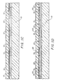
- the conductors 12 and 18 are separated from each other by a gap 22, as seen best in Figure 1D.
- the distance between the conductors 12 and 18 being about 10 micrometers since each of the resilient insulating strips 14 extend about 10 micrometers below the y-conductors 18.
- the 10 micrometer gap 22 normally is filled with air. However, since the interior of the touchpad is preferably sealed, as will be described presently, inert gas such as nitrogen or argon may be used, alternatively. However, normally an air gap is sufficient.
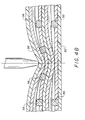
- the flexible membrane 16 deflects as shown in Figure 1 E.
- the resiliency of the resilient insulator strips 20 and flexibility of the membrane 16 allow for the membrane 16 to deflect until portions of the conductors 18 and 12, which are opposed to each other, come into electrical contact with each other.
- the tip of the stylus 24 must be sufficiently small in diameter such that when pressure is applied, the tip forces the conductors together, as shown in that figure. If the tip is too big, then it is believed that it might rest between two insulators 20 without causing a closure event of two of the conductors 12, 18.
- the spacing and width of the conductors is selected based on the precision or resolution of the location desired to be identified. Of course, the more conductors per unit area, the more precise the location that can be identified that is being touched, i.e., the greater the resolution that can be achieved.
- a desirable size is where the copper x-conductors 12 are about 0.008 inch wide, with the spaces therebetween being about 0.012 inch wide, which provides 50 lines per inch.
- the width of the y-conductors 18 on a typical embodiment is 0.012 inch, with the insulators 20 being 0.008 inch wide, thus also providing 50 lines per inch on the flexible membrane 16. It is believed that the conductors at a maximum can be approximately 0.25 inches wide, with the above-mentioned gap 22 of 10 micrometers.
- the conductors are preferably equally spaced and of equal width.
- one or more of the x- or y-conductors can be much thicker.
- a region of the sensor is intended to be a row of dedicated function keys or icons, as is known in the art, a single x-conductor 12 can be as wide as the keys or icons.
- the coarse x-conductor can be printed with and adjacent to the fine x-conductors, as described above, and placed proximate to the y-conductors 18, separated by the insulators 20.
- the electrical circuitry and logic to determine the exact location of contact between conductors 12 and 18 performs a polling function of the various conductors 12 and 18 to determine where the contact is. While this is relatively fast, nevertheless in some instances, it is desirable to decrease the polling time and thus decrease the response time, especially where traces, such as handwriting, are to be mapped.
- the number of electronic device pins becomes very high. For example, a 640 by 480 sensor would need 640 drivers and 480 receivers for a total of 1120 discrete device pins.
- touchpads shown in Figures 2A-2E are provided which, together with circuitry and logic which will be described presently, substantially reduces the time required for the determination of the location of a touch and significantly reduces the complexity of the required circuitry.
- One set is divided into very coarse or broad areas, i.e., having a rather coarse resolution
- the other set is divided into finer or narrow areas, i.e., having a rather fine resolution.
- the coarse areas of resolution are polled to determine the general location of the touch, and the finer areas of resolution within the detected coarse area are polled to determine a more precise location within the general area. This substantially reduces the time needed to determine where the touch has occurred, thus decreasing the response time to a touch in any particular area as will be described presently with respect to the circuitry and logic.
- a substrate 30 is provided which in one embodiment is a glass filled epoxy printed circuit board such as the type previously described. Disposed on the substrate 30 are a plurality of copper coarse x-conductors 32 which are formed as previously described by any suitable technique, such as photolithography and the other printed circuit board fabrication steps mentioned above in regards to the conductors 12.
- a flexible membrane 36 is provided which is similar to membrane 16 of the previously described embodiment and which has formed on one side 37 thereof coarse y-conductors 38, separated by resilient insulating strips of material 40.
- certain parts, including a portion of the coarse y-conductor 38 have been partially cut away for clarity.
- conductive materials or lines 42 Disposed on the opposite surface 41 of the flexible membrane 36 are another set of spaced longitudinally extending conductive materials or lines 42. These fine x-conductors 42 are formed by conventional conductive ink screening as previously described and are spaced and separated by an air gap (not shown) as are the conductors 32.
- a second flexible membrane 46 is also provided on which longitudinally extending fine y-conductors 48 formed of conducting ink and separated by resilient insulating strips 50 are disposed.
- fine y-conductors 48 formed of conducting ink and separated by resilient insulating strips 50 are disposed.
- FIG 2C certain parts, including a portion of the fine y-conductor 48, have been partially cut away for clarity.
- the strips 50 are deposited, as described above, between the conductors 48 and positioned adjacent to the conductors 42.
- the resilient strips 50 can be deposited between the conductors 42 and positioned adjacent to the conductors 48.
- the fine y-conductors 48 are positioned skewed and preferably orthogonally with respect to fine x-conductors 42.
- the width and spacing of the fine x-conductors 42 and the fine y-conductors 48 are substantially the same as the width and spacing of the conductors 12 and 16, respectively, in the previous embodiment.
- the width of coarse conductors 32 and 38 are selected such that they each are wide enough to encompass more than one and preferably up to 16 of the fine conductors 42 and 48, respectively.
- circuitry preferably provides for a polling first to determine the location of the contact of the coarse conductors 32 and 38, to determine a general area of contact. When a general area of contact has been determined, the specific area or more localized area of contact is determined by the location of the contact between the fine conductors 42 and 48.
- the selection of specific materials may vary depending upon the specific characteristics desired in the touchpad. Just as one example, in the alternative, it may be desirable to have the entire touchpad flexible rather than have a rigid base. Such a sensor might be flexed and affixed to a nonplanar surface such as a cylinder or the viewing surface of a cathode ray tube or other display device.
- the substrate 10 or substrate 30 can be replaced with a more flexible substrate 10' or 30', respectively, which indeed could be the same material as the flexible membranes 16, 36 and 46.
- the conductors 12 and 32 would be replaced with a more flexible conductor 12' or 32', respectively, which indeed could be the same material as the flexible conductors 18, 38, 42, and 48.
- Transparent inks well known in the art of LCD panel design allow fabrication of an essentially transparent unit
- Other techniques and other conducting material can be used as can other resilient materials be used between the conductors.
- resilient strips of insulating material can be placed between conductors 12 and 18 or 32 and 38 on the substrate, as shown in Figures 3A, 3B, 4A, and 4B.
- the central substrate 36 can have both conductors and insulators on both sides with the other two substrates 30, 46 only having conductors thereon. Many combinations and permutations are possible.
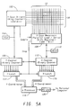
- FIG. 5A a block diagram of the electronics used to interface to the touchpad sensor is shown.
- y-scan drivers 102 In circuit communication with the y-conductors 18 are y-scan drivers 102, one driver per conductor.
- the y-scan drivers 102 comprise a 244-bit self-starting ring counter, which is configured to pass a single logical ONE around the ring responsive to complete cycles of a YCLK 104, which is a free-running square-wave oscillator.
- a YCLK 104 which is a free-running square-wave oscillator.
- the y-conductors 18 are sequentially raised to a voltage corresponding to the logical one.
- the YCLK 104 also causes a y-counter 106 to count.
- the y-counter 106 is a binary up counter configured to reset after counting 244 cycles of the YCLK 104.
- the value of the y-counter 106 is the number of the y-conductor currently at a voltage corresponding to a logical ONE.
- x-scan receivers 108 in circuit communication with the x-conductors 12 are x-scan receivers 108, one receiver per conductor.
- the x-scan receivers 108 comprise a 320-bit parallel load/ serial shift register (PLSSR).
- PLSSR parallel load/ serial shift register
- each y-conductor 18 is at the voltage corresponding to a logical ONE, the value of each of the x-conductors is latched into a corresponding bit of the PLSSR.
- all the x-values are shifted, one at a time, responsive to complete cycles of an XCLK 110, which is a free-running square-wave oscillator.
- the XCLK 110 also causes an x-counter 112 to count.
- the x-counter 112 is a resettable binary up counter configured to count up responsive to complete cycles of the XCLK 110.
- the value of the x-counter 112 is the number of the x-conductor currently being shifted out of the PLSSR.
- the y-counter contains the y-coordinate of the touched region and the x-counter contains the x-coordinate of the touched region. Therefore, the counters are configured to disable counting responsive to a logical ONE being detected at one of the x-conductor values.
- the coordinates stored in the disabled counters 106, 112 are latched into a y-latch 114 and an x-latch 116.
- the values are read by a microprocessor 118 or some other suitable processor and are transmitted via an RS-232 driver 120 to the attached personal computer (not shown).
- FIG. 5B a schematic circuit diagram of one embodiment of the circuit if Figure 5A is shown.
- the circuitry is implemented in eleven programmable logic devices (PLDs) 130a-130k, a microcontroller 132, and an RS-232 driver 120. All electronic devices are properly powered by a suitable power supply and power inputs are properly decoupled with decoupling capacitors (not shown), both of which are well known in the art.
- PLDs programmable logic devices
- the microcontroller 132 is an SC80C51 FB-4F40, which is a programmable 8-bit microcontroller manufactured by Philips Components, Ltd., Mul- lard House, Torrington Place, London WC1 E 7HP, United Kingdom, and is available from many distributors. Other microcontrollers can be used.
- the RS-232 driver 120 is an AD232-JR, manufactured by Analog Devices, One Technology Way, P.O. Box 9106, Norwood, MA 02062-9106, and is available from many distributors. Other RS-232 drivers can be used to drive the signals to proper RS-232 levels, as is known in the art.
- the PLDs 130a-130k are MACH230 PLDs, which are manufactured by Advanced Micro Devices, 901 Thompson Place, P.O. Box 3453, Sunnyvale, CA 94088-3000, and are available from many distributors. Other devices can be used to implement the circuitry.
- each of the y-driver outputs YO-Y239 are connected to one of the y-conductors 18 via a small signal diode 136.
- the diodes 136 prevent damage to the EPLDs if two or more y-conductors are shorted together.
- each of the x-receiver inputs XO-X319 are connected to one of the x-conductors 12.
- Each of the x-conductors are pulled down to a logical ZERO via a 10K pull-down resistor 138, to prevent the inputs of the x-receivers from floating.
- DB-9 connector 140 is used to connect the signals of the touchpad to a personal computer (not shown) or other device receiving coordinate data via a multiconductor cable.
- the switches 142, 144 are used as supplemental inputs, similar to the buttons on a so-called “mouse” pointing device.
- the microcontroller 132 reads port P1.7 to determine the state of the switches 142, 144 and sends an RS-232 signal corresponding to the switch state out of its TxD output, as is well known in the art.
- the circuitry of the y-driver PLDs 130a-130e is shown in Figure 5C.
- the SAMPLE, XCLK, and YCLK signals are generated by a clock circuit 150 from a 16 Mhz digital signal 152.
- the 16 MHz signal 152 can be generated by a hybrid oscillator, a crystal and several inverting Schmitt triggers, and other methods well known in the art.
- the YCLK signal is a digital signal that has a 20.5 us period and can be generated by decoding a signal that has a period that is 328 cycles of the 16 MHz clock signal 152.
- the XCLK is the 16 MHz signal 152.
- the y-driver circuit comprises 244 D-flip flops 154 that are connected in a self-starting ring counter configuration 156 with two inverters 156, as is known in the art and shown in Figure 5C.
- the 244 stages are divided between the 5 PLDs 130a-130e. If different density PLDs are used, more or fewer PLDs might be needed to implement all 244 stages.
- the last output of the previous PLD is connected to an input, labeled IN, of the next PLD by a ring counter connection 142, as is show in Figure 5B.
- the counter connections 142 allow the logical ONE in the ring counter 156 to be shifted through all 244 stages with only one data line connecting the PLDs.
- the ring counter 156 generates the 240 y-driver signals YO-Y239, the timing signals FSYNC1-3, and a DUMMY signal.
- the FSYNC signals are used for timing purposes throughout the circuitry.
- each Y line (as well as each FSYNC and the DUMMY signal) is sequentially held to a logical ONE for 328 cycles of the 16 MHz clock (20.5 us).
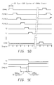
- the details of the SAMPLE signal are shown in Figure 5E.
- the SAMPLE signal was generated using a binary up counter, combinatorial logic, and an R-S latch (all not shown), with the SAMPLE signal being the output of the latch.
- Such circuits are known in the art. Essentially, 318 cycles of the 16 MHz clock into the 328-cycle period of each Y line, the latch is RESET by the logic, thereby allowing the SAMPLE signal to fall low. Eight complete cycles of the 16 MHz clock (500 ns) later, the latch is SET by the logic, thereby causing the SAMPLE signal to rise high again. Two cycles of the 16 MHz clock (125 ns) later, Y n becomes inactive and Y n+i becomes active.
- a y-counter 158 and y-latch 160 are placed in circuit communication as shown.
- the y-counter 158 is an 8-bit binary up counter with count enable and clear, as is known in the art.
- the y-latch is an 8-bit latching register, as is known in the art.
- An AND gate 162 generates a signal that latches the register responsive to the STOP and FSYNC1 signals, also as shown in that figure.
- an R-S latch generates 164 the DISABLE signal responsive to Y239 and FSYNC2, as shown.
- the circuitry of the x-driver PLDs 130f-130k is shown.
- the x-receivers are implemented by a 320- bit parallel load/serial shift register (PLSSR) 170, an R-S latch 172, a 9-bit binary up counter 174 with count enable and clear, a 9-bit latching register 176, and an AND gate 178, placed in circuit communication as shown in that figure.
- PLSSR parallel load/serial shift register
- the 320-bit PLSSR 170 is divided between the six PLDs 130f-130k. If different density PLDs are used, more or fewer PLDs might be needed to implement all 320 stages.
- the stages of the PLSSR 170 can be functional building blocks equivalent to the well known 74165. All six PLDs 130f-130k are connected to the SAMPLE signal and the six PLDs 130f-130k are linked serially by serial connections 180, shown in Figure 5B.
- the output, labelled O, of the previous PLD is connected to the input, labelled I, of the next PLD, as shown in that figure.
- the input of the last PLD 130k is tied to ground.
- the serial connections 180 allow the data in the PLSSR to be shifted through all 320 stages with only one data line connecting the PLDs.
- the 20.5 us value is somewhat arbitrary, but is believed to provide a comfortable medium between very rapid scanning, which is governed by the time- constant of each conductor and which would increase the electromagnetic interference with surrounding electronic devices, and very slow scanning, which would cause the scanning rate to be too slow for digitizing the fluid stylus strokes of, for example, handwriting.
- the y-counter 158 counts responsive to the YCLK.
- the value of the y-counter 158 corresponds to the y-conductor currently being driven.
- the y-counter 158 is configured to be reset to OOH responsive to YCLEAR. YCLEAR is asserted responsive to a completed scan of all y-conductors.
- the SAMPLE signal is asserted by placing it at a logical ZERO and placing it at a logical ONE 500 ns later, as shown in Figure 5E.
- the PLSSR 170 latches the contents of all the x-conductors 12. Normally, all the latched x-conductor values will be at logical ZERO. If the y-conductor that is being driven to a logical ONE is touching one of the x-conductors in the manner shown in Figure 1 E, then one of the latched x-conductor values will also be a logical ONE.
- the PLSSR 170 begins sequentially shifting all the x-conductor values responsive to the XCLK and sequentially inputting them to the R-S latch 172.
- the x-counter 174 counts responsive to the XCLK.
- the value of the x-counter 174 corresponds to the x-conductor the value of which is being shifted past the R-S latch.
- the x-counter 174 is configured to be reset responsive to XCLEAR. XCLEAR resets the x-counter to OOH after all the x-conductor values have been shifted past the R-S latch 172, unless a ONE is detected, in which case the x-counter is cleared after the x-counter value has been latched into the x-latch 176 and before YO is driven.
- each y-conductor 18 is sequentially raised to a voltage corresponding to a logical ONE. While each y-conductor is a logical ONE, the value of all the x-conductors 12 are simultaneously latched and then very rapidly serially shifted to detect the presence of a logical ONE, which indicates a closure event as shown in Figure 1 E.
- the R-S latch 164 clears the DISABLE signal responsive to Y239, thereby signaling to the microcontroller 132 that data is about to change and therefore disabling data reads by the microcontroller 132.
- the output of the R-S latch 172 becomes a logical ONE thereby asserting the STOP signal.
- the y-counter 158 and the x-counter 174 stop counting, even though the PLSSR 170 continues to shift the x-conductor values past the R-S latch 172 and the ring counter 156 continues to pass the logical ONE from one stage to the next.
- the PLSSR 170 continues to shift the x-conductor values past the R-S latch 172 and the ring counter 156 continues to pass the logical ONE from one stage to the next.
- the STOP signal remains asserted until the FSYNC3 signal of the next cycle becomes active.
- the values in the counters 158, 174 are latched into their respective latches 160, 176.
- the R-S latch 164 sets the DISABLE signal, thereby signaling to the microcontroller 132 that data is latched and available, thereby enabling data reads by the microcontroller 132.
- the microcontroller 132 periodically polls the values latched in the latches 160, 176 responsive to the DISABLE signal.
- the microcontroller 132 then encodes the data into a format suitable for serial transmission over the serial line to the personal computer.
- the exact data encoding algorithm is not critical and depends entirely upon the software driver executing on the computer system; different software drivers might require the data to be different formats, as known to those skilled in the art.
- the data must match the software on the computer system. Alternatively, the data can be compressed using any of the well known compression algorithms.
- the encoded values are transmitted out the TxD output of the microcontroller 132 via the RS-232 driver 120 to pin 2 of the DB-9 connector 140.
- the Y lines can be defaulted to a logical ONE and a logical ZERO passed around the ring counter 156.
- the drivers and receivers need not be implemented in PLDs. Rather, an application-specific integrated circuit (ASIC) could be designed and fabricated to perform the required interface functions.
- the 244-bit ring counter 156, the 320-bit PLSSR 170, and the other circuitry can be implemented on a single massive ASIC. Such an ASIC might use active pullups and pulldowns instead of the passive pull-down resistors 138.
- Such circuits are known in the art and use, for example, two NPN transistors, with the collector of the first connected to the emitter of the second, the emitter of the first connected through a resistor to a voltage associated with a logical ONE, the collector of the second connected through a resistor to a voltage near ground, the bases of the transistors connected to respective driver circuitry, and the tied emitter-collector connected to the x-conductors.
- the circuitry includes coarse y-drivers 190, coarse x-receivers 192, fine y-drivers 194, and fine x-receivers 196 all in circuit communication with coordinate determining circuitry 198.
- each of the coarse y-drivers 190 drives a single coarse y-conductor 32.
- each of the coarse x-receivers 192 receives data from a single coarse x-conductor 38.
- each of the fine y-drivers 194 drives more than one fine y-conductor 42.
- each of the fine x-receivers 196 receives data from more than one fine x-conductor 48.
- the ratio is four fine conductors per coarse conductor along both axes.
- Preferably a ratio of 16 fine conductors per coarse conductor along both axes would be used.
- the coordinate determining circuitry 198 can be designed very similarly to the circuits of Figures 5B-5F.
- a pair of ring counters can be used to sequentially drive the coarse and fine y-conductors 32, 42.
- a pair of parallel load/serial shift registers can be used to simultaneously sample the coarse and fine x-conductors 38, 48.
- the circuitry 198 differs from that in Figures 5B-5F in that the intersection of the coarse conductors 32, 38 and the intersection of the fine conductors 42, 48 are used to determine the exact location of the touched region.
- the coarse intersection might indicate that the touch is four coarse rows down and five coarse columns over and the fine intersection might indicate that the touched location is three fine rows down and two fine columns over.
- the exact location would be determined by the fine value plus the coarse value times the number of fine conductors per coarse conductor. In the above example the exact location would be 19 (3+4x4) fine y-conductors down by 22 (2 + 5x4) fine x-conductors over.
- the coordinate determining circuitry 198 can be implemented with two counting inputs: a count-by-four input and a count-by-one input.
- the two counters would count until an intersection is detected.
- the counters would first count by fours (i.e., count by the number of fine conductors per coarse conductors on that axis) until a coarse intersection is detected and then count by ones until a fine intersection is detected.
- Many circuits are possible and within the skill of those skilled in the art.
- the 320-by-240 circuit of Figure 5B requires 560 drivers and receivers: 240 y-drivers and 320 x-receivers.
- a dual sensor of the same 320-by-240 resolution could be made with 16 fine y-conductors per coarse y-conductor and 16 fine x-conductors per coarse x-conductor.
- a coordinate determining circuit 198 to interface to such a 320-by-240 dual sensor would need only 67 drivers and receivers: 15 individual coarse y-drivers, 20 individual coarse x-receivers, 16 individual fine y-drivers, and 16 individual x-receivers.
- either the coarse and fine y-drivers or the coarse and fine x-receivers can be shared, thereby further reducing the driver and receiver count to 51. That is, the y-drivers can each drive one coarse y-conductor and sixteen fine y-conductors.
- the x-receivers can each receive data from one coarse x-conductor and sixteen fine x-conductors.
- the dual sensor greatly reduces the number of drivers and receivers needed to interface to the circuit.
- the circuits require one device pin per driver and one device pin per receiver.
- the circuit of Figure 5B has 560 drivers and receivers requiring 560 device pins and therefore used nine large EPLDs, which could only be replaced by an equally large ASIC or ASICs.
- the device described in the above paragraph can be made with 67 or as little as 51 drivers and receivers, thereby allowing the entire circuit to be designed into a single EPLD or a very small ASIC.
- the reduction in pin-count is virtually an order of magnitude less. Consequently, a much smaller and less costly electronic interface circuit can be used with the dual sensor.
- the conductors were shown as being rail-like. That is, the conductors were shown as being shaped substantially like rectangular parallelopipeds with one axis substantially greater in length than either of the other two axes. However, other conductor shapes are possible.
- the possible intersection area is relatively small in comparison to the total area of the touchpad sensor surface.
- Figure 7A shows one pattern of conductors 200 that results in significantly fewer blind spots.
- the pattern consists of circular conductive pads 202 connected by conductive isthmuses 204.
- the plurality of conductive paths formed by the pads 202 and the isthmuses 204 are non-intersecting and lie longitudinally, as in the other embodiments.
- the pads 202 and isthmuses 204 can be of the same materials as described in the previous embodiments.
- the pads 202 are circular in shape; however, other pad shapes are possible.
- the pads are such that the total contact area as a percentage of total sensor surface area is higher than that of the embodiment of Figure 1A-1C.
- the size and spacing of the pads and isthmuses depends on the desired resolution of the sensor.
- the pads 202 are substantially the same size and are spaced substantially equidistant from each other.
- the isthmuses are substantially the same size and are spaced substantially equidistant from each other.
- Figure 7B shows a touchpad sensor 210 comprising two of the patterns of Figure 7A.
- the first pattern has pads 202 and isthmuses 204 and the second pattern has pads 212 and isthmuses 214.
- the second pattern is rotated 90 such that the conductive paths of each are skewed and preferably orthogonally to each other.
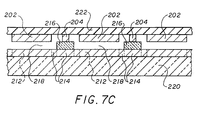
- the two patterns are separated by insulating pads 216 at the intersections of the isthmuses 204, 214 as viewed from the top.
- Figure 7C shows the insulating pads 216, conductive pads 202, 212, and the isthmuses 204, 214.
- the insulating pads 216 are configured such that conductive pads 202, 212 are separated by a gap 218.
- the gap can be air or an inert gas.
- the pads 212 and isthmuses 214 are disposed on a rigid substrate 220 and the pads 202 and isthmuses 204 are disposed on a flexible substrate 222.
- the conductive pads 202, 212 and conductive isthmuses 204, 214 can be made of the same materials and applied in the manner as the conductors described above.
- the insulating pads 216 can be made of the same materials and applied in the manner as the insulators described above.
- the contact area of the embodiment of Figure 7B is approximately 40% of the total area of the sensor surface. If the circular conductive pads are increased in size until they are just separated, the contact area can be approximately 75% of the total sensor surface area.
- the electronics for driving the embodiment of Figure 7B is very similar if not identical to that shown in Figures 5A-5F.
- One possible modification is to slightly skew the resulting coordinates because in the sensor of Figures 1A-1C the adjacent contact areas are horizontal and vertical and in the embodiment of Figure 7B, the adjacent contact areas lie along diagonals.
- FIG 8 the electrical connections of the various conductors to the circuit components is shown, somewhat diagrammatically.
- the many integrated circuits of Figures 5A-5E are mounted on two double-sided printed circuit boards 10, 300.
- the printed circuit board 10 is the same board 10 used as the substrate for the embodiment of the sensor shown in Figures 1A-1E.
- the conductors 12 on the one side 304 of the substrate 10 are connected through vias 302 formed through the substrate 10 to the circuitry 130f-130k via circuit traces 308 on the opposite side 306 of the substrate 10.
- the other circuitry 130a-130e is disposed on the second PCB 300 and electrically connected to printed circuit traces 309.
- the conductors 18 on the membrane 16 are connected to electrical circuitry 130a-130e via a 240-line flexible connector cable 310 having circuit traces 312 thereon.
- the cable 310 can be made of the same material as the other flexible membranes 16, 36, and 46.
- the circuit traces 312 can be made of conductive ink like the conductors 18, 38, 42, and 48 and applied as such.
- the connection of the cable 310 to the conductors 18 and traces 309 is preferably by conducting adhesive 314.
- the adhesive can be an anisotropic conductive adhesive such as an epoxy with conducting particles suspended therein, as is known in the art.
- the conductors are aligned, the adhesive is applied, and the bond area is heated, and held under pressure until the epoxy sets.
- the anisotropic adhesive provides electrically conducting adhesion between the conductors 312 and 18 and conductors 312 and 309 and non-electrically conducting adhesion elsewhere.
- the substrate 300 also is preferably formed of glass-filled epoxy, such as FR4 and has mounted on the top surface additional circuit chips to perform the functions of Figure 5A-5F.
- Various other components are mounted on the boards 10 and 300, such as the diodes 136 and resistors 138, both in surface mount form.
- the boards 10 and 300 are interconnected by stand-offs (not shown), which are well known in the art. The same arrangement of circuitry is used for the dual sensor of the present invention.
- the two substrates 10, 16 can be sealed with a sealing material 316.
- a sealing material 316 Many materials are suitable, such as transfer adhesives and their equivalents and injected adhesives. Such adhesives are known in the art and available from numerous sources, such as the 3M Company.
- the following signals are communicated between the two boards 10, 300 with well known inter-PCB connectors: the 16 MHz clock, SAMPLE, FSYNC1, FSYNC2, FSYNC3, STOP, LXO-LX8, and the power supply sources.
- the entire structure is then enclosed in a sealable case (not shown), which can be hermetically sealed, as known by those skilled in the art.
- This case may include an additional flexible membrane covering the substrate 16 to improve its scratch and wear resistance.
Abstract
A touchpad using a dual sensor comprising two touchpad sensors having different resolutions being sandwiched to form a single sensor. The two touchpad sensors are configured and positioned such that a single touch of a finger, stylus, or the like is capable of being detected by both sensors. The dual sensor is capable of being scanned more quickly than single sensors and is capable of being interfaced by significantly fewer drivers and receivers.
In one embodiment, the touchpads to be sandwiched to form the dual sensor comprise a first plurality of electrically conductive strips positioned proximate to a second plurality of electrically conductive strips. The conductive strips in each plurality lie substantially in a single plane and the two pluralities are skewed relative to one-another in plan view. Ideally, the pluralities are aligned orthogonally. The conductive strips are separated by insulators that extend beyond the surface of the conductors to separate the conductors of one plurality from the conductors of the other plurality until a localized pressure is applied to a region of the pad.
Two such sensors are sandwiched to form an embodiment of the dual sensor of the present invention. When a localized pressure is applied, the conductors and insulators of both sensors deform until a conductor from the first plurality forms an electrically conducting path with at least one conductor from the second plurality.
Description
- The present invention relates generally to input devices for digital electronic systems.
- Touchpads, also known as digital pads, are coordinate type pointing devices used to input coordinate type data to computer systems and computer-controlled devices. A touchpad is typically a pressure-sensitive bounded plane capable of detecting localized pressure at its surface. When a user touches the surface with a finger, stylus, or the like, the circuitry associated with the touchpad determines and reports to the attached computer system the coordinates of the location touched. In response, the computer performs the function, if any, associated with the location pressed.
- Typically one or more regions of the touchpad are assigned to certain functions within the system. The user is made aware of what function is associated with each region by a template. A template is a sheet with a graphic design and is typically placed over and in contact with the touchpad surface. The graphic design typically maps out regions of the touchpad surface and the regions are typically labeled to provide a reminder to the user as to the functions associated with the various mapped regions.
- A touchpad's sensor is the heart of the touchpad. Several types of touchpad sensors are known in the art, such as switch closure type sensors. For example, a keyboard sensor having matrix of membrane switches is disclosed in U.S. Patent No. 4,736,190 to Florella. A touch by a finger on a key causes a closure event between a pair of conductors. As with other switch closure type sensors, the location of the touch is detected using a bank of digital signal drivers and a bank of digital signal receivers.
- Other devices known in the art are very complex. For example, U.S. Patent No. 4,529,959 to Ito et al. discloses a sensor for a coordinate type input device comprising a braided lattice of conductors embedded in a compressible open-cell insulating material sandwiched between two insulating layers coated with a resistive material. Another sensor is shown in U.S. Patent No. 4,455,450 to Margolin. This sensor involves resistive sheets sealed into a "pillow" form.
- Typically one digital signal driver per row and one digital signal receiver per column is used. In high-resolution devices, the large number of drivers required significantly adds to the cost of the scanning electronics and, therefore, the cost of the touchpad. For example, a touchpad that is 640 rows by 480 columns will require 480 drivers and 640 receivers for a total of 1120 (640 + 480 = 1120) individual device pins. An electrical device having 1120 pins can be prohibitively expensive using programmable logic devices (PLDs) or even an application specific integrated circuit (ASIC).
- In addition, high-density devices can have a relatively slow response time because each driver is sequentially activated and each receiver must be checked for each driver. A matrix that is 640 rows by 480 columns can require as many as 307,200 individual scans, because each row is sequentially driven by the drivers and each column must be scanned for each driven row.
- It is therefore desirable to provide a high-resolution touchpad sensor without the need for a correspondingly large number of drivers and receivers.
- It is also desirable to provide a touchpad sensor suitable for simplified scanning with a corresponding increase in the scanning bandwidth.
- In accordance with the present invention, there is now provided a dual sensor comprising: a first touchpad sensor having a first resolution; and a second touchpad sensor substantially the same size as said first touchpad sensor, having a second resolution, and positioned proximate to said first touchpad sensor; wherein said first touchpad resolution is different from said second touchpad resolution; and wherein said first and second touchpad sensors are configured and positioned such that a single touch of a finger, stylus, or the like is detectable by both said first touchpad sensor and said second touchpad sensor.
- Viewing the present invention from another aspect, there is now provided a method of fabricating a touchpad sensor comprising the steps of: (a) affixing a first plurality of conductors onto a first substrate; (b) affixing a second plurality of conductors onto the first side of a second substrate; (c) affixing a first plurality of insulators onto the first side of said second substrate; (d) affixing a third plurality of conductors onto the second side of said second substrate; (e) affixing a second plurality of insulators onto the second side of said second substrate; (f) affixing a fourth plurality of conductors onto a third substrate; and (g) positioning said first, second, and third substrates such that said insulators of said first plurality of insulators are in physical contact with said first plurality of conductors, said insulators of said second plurality of insulators are in physical contact with said fourth plurality of conductors, said insulators of said first plurality of insulators prevent physical contact between said conductors of said first and second pluralities of conductors until a localized pressure is applied, said insulators of said second plurality of insulators prevent physical contact between said conductors of said third and fourth pluralities of conductors until a localized pressure is applied, said first and second pluralities of conductors are skewed in plan view, said third and fourth pluralities of conductors are skewed in plan view.
- Viewing the present invention from still another aspect, there is now provided a dual sensor comprising: a first plurality of conductors that are flexible, spaced from adjacent conductors by a first plurality of insulators, and substantially parallel to each other; a second plurality of conductors proximate to said first plurality of conductors, substantially parallel to each other, skewed with respect to said first plurality of conductors in plan view, and spaced from adjacent conductors of said second plurality of conductors by a second plurality of insulators; a stylus surface proximate to said first plurality of conductors for accepting pressure from a finger, a stylus, or the like; a third plurality of conductors that are flexible, positioned proximate to said first plurality of conductors, spaced from adjacent conductors by a third plurality of insulators, and substantially parallel to each other; and a fourth plurality of conductors proximate to said third plurality of conductors, substantially parallel to each other, skewed with respect to said third plurality of conductors in plan view, and spaced from adjacent conductors of said fourth plurality of conductors by a fourth plurality of insulators; wherein each of said conductors of said first and second pluralities of conductors and each of said insulators of said first and second pluralities of insulators is configured and positioned such that each of said first plurality of conductors has two states: a relaxed state and a flexed state; said relaxed state being characterized by said conductor not being in electrically conducting contact with any of said conductors of said second plurality of conductors; and said flexed state being characterized by said conductor being in electrically conducting contact with at least one conductor of said second plurality of conductors; wherein each of said conductors of said first and second pluralities of conductors and each of said insulators of said first and second pluralities of insulators is further configured such that the asserting a predetermined amount of pressure from a finger, stylus, or the like to said stylus surface causes at least one of said first plurality of conductors in said relaxed state to enter said flexed state and removing the predetermined amount of pressure from said stylus surface causes said at least one of said conductors in said flexed state to enter said relaxed state; wherein each of said conductors of said third and fourth pluralities of conductors and each of said insulators of said third and fourth pluralities of insulators is configured and positioned such that each of said third plurality of conductors has two states: a relaxed state and a flexed state; said relaxed state being characterized by said conductor not being in electrically conducting contact with any of said conductors of said fourth plurality of conductors; and said flexed state being characterized by said conductor being in electrically conducting contact with at least one conductor of said fourth plurality of conductors; and each of said conductors of said third and fourth pluralities of conductors and each of said insulators of said third and fourth pluralities of insulators is further configured such that the asserting a predetermined amount of pressure from a finger, stylus, or the like to said stylus surface causes at least one of said third plurality of conductors in said relaxed state to enter said flexed state and removing the predetermined amount of pressure from said stylus surface causes said at least one of said conductors in said flexed state to enter said relaxed state.
- In a preferred embodiment of the present invention, a touchpad sensor is provided having two integrated sensors: a low- resolution sensor and a high-resolution sensor. The two sensors are positioned such that they overlap and such that applying pressure with a finger, stylus, or the like causes two events: a detection event at the first sensor and a detection event at the second sensor.
- In one arrangement of the dual sensor of the present invention, the sensors have a first plurality of electrically conductive strips positioned proximate to a second plurality of electrically conductive strips. The conductive strips in each plurality lie substantially in a single plane and the two pluralities are skewed relative to one-another when viewed from the top. Ideally, the pluralities are aligned orthogonally. In both pluralities, the conductive strips are separated by insulating strips that extend beyond the surface of the conductors to separate the conductors of one plurality from the conductors of the other plurality until a localized pressure is applied to a region of the pad. When a localized pressure is applied, the conductors and insulators deform until a conductor from the first plurality forms an electrically conducting path with at least one conductor from the second plurality.
- In a dual sensor arrangement of the present invention, two of the sensors described above, one of which has wide conductors and the other of which has narrow conductors, are sandwiched in overlapping relationship to form a dual sensor with first, second, third, and fourth pluralities of conductors. The wide conductors are relatively few in number as compared to the narrow conductors. When a localized pressure is applied, the conductors and insulators deform until a conductor from the first plurality forms an electrically conducting path with at least one conductor from the second plurality and a conductor from the third plurality forms an electrically conducting path with at least one conductor from the fourth plurality.
- This dual sensor greatly simplifies the scanning process. First, the wide conductors are scanned using drivers and receivers. Locating the position of the touch at the intersection of the wide row and wide column provides the position of the touch to within a rectangular area the size of one wide conductor. To determine the location of the touch to the accuracy of the narrow conductors, all the narrow conductors need not be scanned. Only the narrow conductors corresponding to that intersection need be scanned. Thus, the scanning process is simplified by significantly reducing the number of narrow conductors to be scanned; the number of narrow conductors to be scanned has been reduced to the number covered by the intersection of the wide conductors. Thus, the number of narrow scan drivers and receivers are reduced by the ratio of narrow conductors to wide conductors. Hundreds of driver scans can be avoided, thereby avoiding hundreds of thousands of overall scans. Thus, the time-savings associated with the dual sensor scan of the present invention can be quite significant.
- The dual sensor embodiment described above is not overly complex and can be manufactured using standard lithography techniques and relatively inexpensive materials. Standard driver-receiver banks can be used to scan the touchpad sensor and detect the location of the touch.
- This dual sensor concept can also be applied to sensors of different technologies, such as the devices mentioned in the Background, above. The dual sensor simplifies the scanning process regardless of the technology of the two sensors involved.
- It is therefore an advantage of the present invention to provide a dual sensor that greatly simplifies and speeds up the scanning process by significantly reducing the number of drivers and receivers needed.
- It is a further advantage of this invention to provide a dual sensor that greatly reduces the cost of the scanner needed to determine the location of the touch by significantly reducing the number of drivers and receivers needed.
- These and other advantages of the present invention will become more apparent from a detailed description of the invention.
- A preferred embodiment of the present invention will now be described, by way of example only, with reference to the accompanying drawings, in which:
- Figure 1A is a perspective view of one embodiment of a single touchpad sensor, two of which form one embodiment of the dual sensor of the present invention;
- Figure 1B is an exploded perspective view of the single sensor shown in Figure 1A;
- Figure 1 C is a front elevational view of the single sensor shown in Figure 1A with parts broken away for clarity;
- Figure 1 D is a side elevational view of the single sensor shown in Figure 1A with parts broken away for clarity;
- Figure 1 E shows the effects of pressure from a stylus on the sensor shown in Figure 1 D;
- Figure 2A is a perspective view of an embodiment of the dual sensor of the present invention;
- Figure 2B is an exploded perspective view of the embodiment of the present invention shown in Figure 2A;
- Figure 2C is a front elevational view of the embodiment shown in Figure 2A with parts broken away for clarity;
- Figure 2D is a side elevational view of the embodiment shown in Figure 2A with parts broken away for clarity;
- Figure 2E shows the effects of pressure from a stylus on the embodiment of the present invention shown in Figure 2C;
- Figure 3A is a front elevational view of another embodiment of the single sensor with parts broken away for clarity;
- Figure 3B shows the effects of pressure from a stylus on the single sensor shown in Figure 3A;
- Figure 4A is a front elevational view of another embodiment of the dual sensor of the present invention with parts broken away for clarity;
- Figure 4B shows the effects of pressure from a stylus on the embodiment of the present invention shown in Figure 4A;
- Figure 5A is an electrical block diagram showing the major components of an embodiment of an electrical circuit for interfacing to the touchpad sensor shown in Figures 1A-1E;
- Figure 5B is an electrical schematic diagram showing an implementation of the electrical circuit for interfacing to the touchpad sensor shown in Figures 1 A-1 E;
- Figure 5C is an electrical schematic diagram showing the details of the y-drivers for the electrical circuit for interfacing to the touchpad sensor shown in Figures 1A-1E;
- Figures 5D and 5E are waveform diagrams showing the relationships between several selected signals of the circuit shown in Figures 5B and 5C;
- Figure 5F is an electrical schematic diagram showing the details of the x-receivers for the electrical circuit for interfacing to the touchpad sensor shown in Figures 1A-1E;
- Figure 6 is an electrical block diagram showing the major components of an embodiment of an electrical circuit for interfacing to the dual sensor shown in Figures 2A-2E;
- Figure 7A is a top view of one layer of conductors of yet another embodiment of the touchpad sensor;
- Figure 7B is a top view of the embodiment of the sensor shown partially in Figure 7A;
- Figure 7C is a side elevational view of the embodiment shown in Figure 7B taken along the
line 7C-7C; and - Figure 8 is a side elevational view of the construction of the embodiment shown in Figures 1A-1E with the integrated circuits embodying the circuitry of Figures 5A-5F.
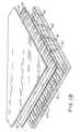
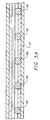
- Referring now to the drawings and for the present to Figures 1A-1E, one embodiment of a touchpad sensor is shown. This embodiment includes a first plurality of non-intersecting longitudinally extending spaced conductors formed on a first substrate, and a second plurality of non-intersecting conductors longitudinally extending on a second flexible substrate, separated by strips of resilient insulating material. The substrates are arranged to support the conductors in superposed spaced relationship, and with the first and second sets of conductors being positioned to extend skewed and preferably orthogonally with respect to each other and maintained by the insulating strips normally spaced from each other. With this configuration, pressure exerted upon the flexible substrate overcomes the resilience of the resilient insulating strips and which, together with the flexibility of the substrate and insulating strips, allows the portions of the first and second conductors at the location of the pressure to come into electrical contact with each other. This location of contact is defined in an X-Y axis on the planes of the conductors and can be translated by circuitry to be explained presently to a signal corresponding to the location of the pressure on the touchpad.
- Specifically in this embodiment, a relatively
rigid substrate 10 is provided which preferably is formed of glass-filled epoxy such as an epoxy circuit board material known as FR4. Typically, this board is about 2 mm thick, although other insulating materials of various thickness can be used. A plurality of spaced non-intersecting longitudinally extendingx-conductors 12 are formed on thesubstrate 10. These x-conductors preferably are substantially equal in spacing and width and are preferably formed of copper with a Gold flash using conventional printed circuit board fabrication photoresist techniques. Either positive or negative photoresist may be used, and either additive or subtractive plating may be used, which techniques are well known in the art. One particularly desirable technique is to start with a substrate having 1 oz. copper plated thereon, and by lithographic technique expose and develop the photoresist and etch the revealed copper to form the desired conduction pattern under the remaining resist. This resist is then removed and the copper plated up to the desired structure--normally .036 mm. A Gold flash is then provided on the copper for oxidation resistance. This technique is well known in the printed circuit board industry. Thus, a plurality of longitudinally extending spacedx-conductors 12 are formed on thesubstrate 10. Of course, other techniques and materials such as screen printing of conductive inks could be used. - The touchpad also includes a
flexible membrane 16 which preferably is formed of a polyester such as that sold by International Chemical Industries (ICI) of Great Britain or hard coated polyester sold by the E.I. du Pont Company. The preferred material is ICI Melinex ST525, which is manufactured by ICI Films, Wilton Centre, PO Box 90, Middlesbrough, Cleveland, TS90 8JE, United Kingdom. A hardened version of the ST525 is preferred and available from Cadillac Plastics, Rivermead Road, Westlea, Swindon, Wiltshire, United Kingdom. Membrane thicknesses of 0.003 inch and 0.005 inch have proved to be effective. - Deposited on the
flexible membrane 16 are a plurality of non-intersecting y-conductors 18 which extend longitudinally thereon. In Figure 1 C, certain parts, including a portion of the y-conductor 18, have been partially cut away for clarity. The y-conductors 18 preferably are substantially equal in spacing and width and are preferably formed by printing with conductive ink using conventional mask printing techniques and conventional conducting inks such as epoxies with silver particles contained therein. One suitable screen printable conductive ink is available from Acheson Colloids, Prince Rock, Plymouth, Devon, United Kingdom. - Between the y-
conductors 18 are strips of resilient insulatingmaterial 20. The strips of insulatingmaterial 20 are preferably Acheson ML25227, which is manufactured by Acheson Colloids, Prince Rock, Plymouth, Devon, United Kingdom, and available from NFI Electronics Ltd., Dodnor Industrial Estate, Newport, Isle of Wight, P030 5XB, England. However, any material that is easily printed or applied in fine strips and that has sufficient flexibility (15,000 cycles measured under ASTM D2176 is sufficient), dielectric strength (125 KV/mm measured under ASTM D149 is sufficient), and surface resistivity (1013 ohms/square measured under ASTM D257 is sufficient) can be used to make the insulating strips 20. The insulating strips 20 are applied using conventional screen printing techniques, as known to those skilled in the art. - The thickness of the y-
conductors 18 preferably is about 12 micrometers, and the thickness of the resilient insulatingstrips 20 is approximately 22 micrometers. Therefore, the insulatingstrips 20 extend about 10 micrometers below theconductors 18. Consequently, when theinsulators 20 are placed in contact with theconductors 12, as will be discussed presently, theconductors 12 are separated from theconductors 18 by approximately 10 micrometers. - In the figures, the edges of the
conductors 18 are touching the edges of theinsulators 20. This is an ideal condition. In practice, the printing mask for the insulators is slightly narrower than the spaces between theconductors 18. Therefore, when the insulating material is applied, a small gap exists between theinsulator 20 and theadjacent conductor 18. The width of the gap (not shown) is not critical; it should be such that when the insulating material is applied and it spreads, no portion of the conductor is covered by the insulating material. - Also in the figures, each
conductor 18 has an insulatingstrip 20 on either side of it. In the alternative, fewer insulatingstrips 20 might be sufficient to keep theconductors strip 20 might be replaced with an air gap (not shown) between theconductors 18, in the manner theconductors 12 are separated from each other, as will be explained below. - As can best be seen in Figures 1 B, 1 C, and 1D, the
substrate 10 andflexible membrane 16 are placed in superposed relationship with each other, with theconductors conductors strips 20 are in contact with the x-conductor 12 on thesubstrate 10. Locating pins (not shown) are formed on thesubstrate 20 and coact with holes (not shown) in themembrane 16 to properly align theconductors strips 20 in contact withx-conductors 12, theconductors gap 22, as seen best in Figure 1D. The distance between theconductors conductors 18. The 10micrometer gap 22 normally is filled with air. However, since the interior of the touchpad is preferably sealed, as will be described presently, inert gas such as nitrogen or argon may be used, alternatively. However, normally an air gap is sufficient. - When a sufficient pressure is exerted such as by the point of a
stylus 24, or a finger or the like, theflexible membrane 16 deflects as shown in Figure 1 E. The resiliency of the resilient insulator strips 20 and flexibility of themembrane 16 allow for themembrane 16 to deflect until portions of theconductors stylus 24 must be sufficiently small in diameter such that when pressure is applied, the tip forces the conductors together, as shown in that figure. If the tip is too big, then it is believed that it might rest between twoinsulators 20 without causing a closure event of two of theconductors insulators 20 enough to cause sufficient flexing to cause theconductors conductors conductors - The spacing and width of the conductors is selected based on the precision or resolution of the location desired to be identified. Of course, the more conductors per unit area, the more precise the location that can be identified that is being touched, i.e., the greater the resolution that can be achieved. In a typical touchpad, a desirable size is where the
copper x-conductors 12 are about 0.008 inch wide, with the spaces therebetween being about 0.012 inch wide, which provides 50 lines per inch. The width of the y-conductors 18 on a typical embodiment is 0.012 inch, with theinsulators 20 being 0.008 inch wide, thus also providing 50 lines per inch on theflexible membrane 16. It is believed that the conductors at a maximum can be approximately 0.25 inches wide, with the above-mentionedgap 22 of 10 micrometers. - In the above embodiment, the conductors are preferably equally spaced and of equal width. In the alternative, one or more of the x- or y-conductors can be much thicker. For example, if a region of the sensor is intended to be a row of dedicated function keys or icons, as is known in the art, a single x-conductor 12 can be as wide as the keys or icons. The coarse x-conductor can be printed with and adjacent to the fine x-conductors, as described above, and placed proximate to the y-
conductors 18, separated by theinsulators 20. - As will be described presently, the electrical circuitry and logic to determine the exact location of contact between
conductors various conductors - To these ends, the embodiment of touchpads shown in Figures 2A-2E are provided which, together with circuitry and logic which will be described presently, substantially reduces the time required for the determination of the location of a touch and significantly reduces the complexity of the required circuitry. In this embodiment, there are two sets of pairs of superposed conductors, each of which sets are actuated by a single touch of a stylus or finger or the like. One set is divided into very coarse or broad areas, i.e., having a rather coarse resolution, and the other set is divided into finer or narrow areas, i.e., having a rather fine resolution. As will be described presently, the coarse areas of resolution are polled to determine the general location of the touch, and the finer areas of resolution within the detected coarse area are polled to determine a more precise location within the general area. This substantially reduces the time needed to determine where the touch has occurred, thus decreasing the response time to a touch in any particular area as will be described presently with respect to the circuitry and logic.
- Referring now to Figures 2A-2E, an embodiment of the dual sensor of the present invention is shown. A
substrate 30 is provided which in one embodiment is a glass filled epoxy printed circuit board such as the type previously described. Disposed on thesubstrate 30 are a plurality of coppercoarse x-conductors 32 which are formed as previously described by any suitable technique, such as photolithography and the other printed circuit board fabrication steps mentioned above in regards to theconductors 12. Aflexible membrane 36 is provided which is similar tomembrane 16 of the previously described embodiment and which has formed on oneside 37 thereof coarse y-conductors 38, separated by resilient insulating strips ofmaterial 40. In Figure 2C, certain parts, including a portion of the coarse y-conductor 38, have been partially cut away for clarity. The coarse y-conductors 38 are preferably formed of conducting ink similar to theconductors 18 and the resilient insulating strips ofmaterial 40 are preferably the same material as the material for insulatingstrips 20 in the previous embodiment. Up to this point, the structure is substantially similar to that of the previously described embodiment, other than the width of theconductors - Disposed on the
opposite surface 41 of theflexible membrane 36 are another set of spaced longitudinally extending conductive materials or lines 42. Thesefine x-conductors 42 are formed by conventional conductive ink screening as previously described and are spaced and separated by an air gap (not shown) as are theconductors 32. - A second
flexible membrane 46 is also provided on which longitudinally extending fine y-conductors 48 formed of conducting ink and separated by resilient insulatingstrips 50 are disposed. In Figure 2C, certain parts, including a portion of the fine y-conductor 48, have been partially cut away for clarity. Thestrips 50 are deposited, as described above, between theconductors 48 and positioned adjacent to theconductors 42. In the alternative, theresilient strips 50 can be deposited between theconductors 42 and positioned adjacent to theconductors 48. The fine y-conductors 48 are positioned skewed and preferably orthogonally with respect tofine x-conductors 42. In this embodiment, there is anupper gap 52 between theupper conductors lower gap 54 between thelower conductors text accompanying gap 22. In this embodiment, the width and spacing of the fine x-conductors 42 and the fine y-conductors 48 are substantially the same as the width and spacing of theconductors coarse conductors fine conductors coarse conductors fine conductors 42 and 48 (i.e., 16 x 16 = 256). Hence, when a gross area of contact has been identified by contact betweencoarse conductors fine conductors fine conductors fine conductors conductors - As can be seen in Figure 2E, when the
stylus 24 puts pressure on theflexible membrane 46, the deflection or deformation therebeneath of bothmembrane 46 andmembrane 36 causes a dual or double superimposed contact action to take place. In one contact action, one of the coarse y-conductors 38 contacts one of thecoarse x-conductors 32, and also one offine x-conductors 42 contacts one of the fine y-conductors 48. As will be described presently, circuitry preferably provides for a polling first to determine the location of the contact of thecoarse conductors fine conductors - Further, it is to be understood that the selection of specific materials may vary depending upon the specific characteristics desired in the touchpad. Just as one example, in the alternative, it may be desirable to have the entire touchpad flexible rather than have a rigid base. Such a sensor might be flexed and affixed to a nonplanar surface such as a cylinder or the viewing surface of a cathode ray tube or other display device.
- As shown in Figures 3A-3B and 4A-4B, in such a case, the
substrate 10 orsubstrate 30 can be replaced with a more flexible substrate 10' or 30', respectively, which indeed could be the same material as theflexible membranes conductors flexible conductors conductors - In the alternative, the
central substrate 36 can have both conductors and insulators on both sides with the other twosubstrates - Referring now to Figure 5A, a block diagram of the electronics used to interface to the touchpad sensor is shown.
- In circuit communication with the y-
conductors 18 are y-scan drivers 102, one driver per conductor. The y-scan drivers 102 comprise a 244-bit self-starting ring counter, which is configured to pass a single logical ONE around the ring responsive to complete cycles of aYCLK 104, which is a free-running square-wave oscillator. As the logical ONE is passed around the ring, the y-conductors 18 are sequentially raised to a voltage corresponding to the logical one. As each y-conductor 18 is raised to a logical ONE, theYCLK 104 also causes a y-counter 106 to count. The y-counter 106 is a binary up counter configured to reset after counting 244 cycles of theYCLK 104. Thus, the value of the y-counter 106 is the number of the y-conductor currently at a voltage corresponding to a logical ONE. - Likewise, in circuit communication with the x-conductors 12 are
x-scan receivers 108, one receiver per conductor. Thex-scan receivers 108 comprise a 320-bit parallel load/ serial shift register (PLSSR). During the time each y-conductor 18 is at the voltage corresponding to a logical ONE, the value of each of the x-conductors is latched into a corresponding bit of the PLSSR. Immediately after latching, all the x-values are shifted, one at a time, responsive to complete cycles of anXCLK 110, which is a free-running square-wave oscillator. As each individual x-conductor value is shifted, theXCLK 110 also causes an x-counter 112 to count. The x-counter 112 is a resettable binary up counter configured to count up responsive to complete cycles of theXCLK 110. Thus, the value of the x-counter 112 is the number of the x-conductor currently being shifted out of the PLSSR. - If the y-conductor that is being driven to a logical ONE is touching one of the x-conductors in the manner shown in Figure 1 E, then one of the latched x-conductor values will also be a logical ONE. On the other hand, if the y-conductor that is at a logical ONE is not touching one of the x-conductors in the manner shown in Figure 1 E, then all of the latched values will be a logical ZERO. Thus, if one of the x-conductor values is a logical ONE, then at the moment that one bit is shifted out of the PLSSR, the y-counter contains the y-coordinate of the touched region and the x-counter contains the x-coordinate of the touched region. Therefore, the counters are configured to disable counting responsive to a logical ONE being detected at one of the x-conductor values.
- The coordinates stored in the
disabled counters latch 114 and an x-latch 116. The values are read by amicroprocessor 118 or some other suitable processor and are transmitted via an RS-232driver 120 to the attached personal computer (not shown). - Referring now to Figure 5B, a schematic circuit diagram of one embodiment of the circuit if Figure 5A is shown. In this embodiment, the circuitry is implemented in eleven programmable logic devices (PLDs) 130a-130k, a
microcontroller 132, and an RS-232driver 120. All electronic devices are properly powered by a suitable power supply and power inputs are properly decoupled with decoupling capacitors (not shown), both of which are well known in the art. - The
microcontroller 132 is an SC80C51 FB-4F40, which is a programmable 8-bit microcontroller manufactured by Philips Components, Ltd., Mul- lard House, Torrington Place, London WC1 E 7HP, United Kingdom, and is available from many distributors. Other microcontrollers can be used. The RS-232driver 120 is an AD232-JR, manufactured by Analog Devices, One Technology Way, P.O. Box 9106, Norwood, MA 02062-9106, and is available from many distributors. Other RS-232 drivers can be used to drive the signals to proper RS-232 levels, as is known in the art. ThePLDs 130a-130k are MACH230 PLDs, which are manufactured by Advanced Micro Devices, 901 Thompson Place, P.O. Box 3453, Sunnyvale, CA 94088-3000, and are available from many distributors. Other devices can be used to implement the circuitry. - The devices are connected in circuit communication, as shown in Figure 5B. As shown in that figure, each of the y-driver outputs YO-Y239 are connected to one of the y-
conductors 18 via asmall signal diode 136. Thediodes 136 prevent damage to the EPLDs if two or more y-conductors are shorted together. Likewise, each of the x-receiver inputs XO-X319 are connected to one of the x-conductors 12. Each of the x-conductors are pulled down to a logical ZERO via a 10K pull-down resistor 138, to prevent the inputs of the x-receivers from floating. - Also shown in Figure 5B is a DB-9
connector 140, a pair ofswitches 10K pullup resistor 146, all in circuit communication as shown in that figure. The DB-9connector 140 is used to connect the signals of the touchpad to a personal computer (not shown) or other device receiving coordinate data via a multiconductor cable. - The
switches microcontroller 132 reads port P1.7 to determine the state of theswitches - The circuitry of the y-
driver PLDs 130a-130e is shown in Figure 5C. As shown in that figure, the SAMPLE, XCLK, and YCLK signals are generated by aclock circuit 150 from a 16 Mhzdigital signal 152. The 16 MHz signal 152 can be generated by a hybrid oscillator, a crystal and several inverting Schmitt triggers, and other methods well known in the art. The YCLK signal is a digital signal that has a 20.5 us period and can be generated by decoding a signal that has a period that is 328 cycles of the 16MHz clock signal 152. In this embodiment, the XCLK is the 16MHz signal 152. - The y-driver circuit comprises 244 D-
flip flops 154 that are connected in a self-starting ring counter configuration 156 with two inverters 156, as is known in the art and shown in Figure 5C. The 244 stages are divided between the 5PLDs 130a-130e. If different density PLDs are used, more or fewer PLDs might be needed to implement all 244 stages. The last output of the previous PLD is connected to an input, labeled IN, of the next PLD by aring counter connection 142, as is show in Figure 5B. Thecounter connections 142 allow the logical ONE in the ring counter 156 to be shifted through all 244 stages with only one data line connecting the PLDs. - The ring counter 156 generates the 240 y-driver signals YO-Y239, the timing signals FSYNC1-3, and a DUMMY signal. The FSYNC signals are used for timing purposes throughout the circuitry. The
flip flops 154 reset such that Q=0 on powerup; therefore, before first cycle of YCLK, the DUMMY signal, the FSYNC signals, and the Y signals are all a logical ZERO. After the first period of YCLK, a ONE appears at FSYNC1 and all the others remain a ZERO. After the next period of YCLK, FSYNC1 changes to a ZERO and FSYNC2 changes to a logical ONE. Successive cycles of YCLK cause the logical ONE to appear to be passed from one D-flip flop to the next, as is known in the art and shown in Figure 5D. As shown in that figure, each Y line (as well as each FSYNC and the DUMMY signal) is sequentially held to a logical ONE for 328 cycles of the 16 MHz clock (20.5 us). - The details of the SAMPLE signal are shown in Figure 5E. The SAMPLE signal was generated using a binary up counter, combinatorial logic, and an R-S latch (all not shown), with the SAMPLE signal being the output of the latch. Such circuits are known in the art. Essentially, 318 cycles of the 16 MHz clock into the 328-cycle period of each Y line, the latch is RESET by the logic, thereby allowing the SAMPLE signal to fall low. Eight complete cycles of the 16 MHz clock (500 ns) later, the latch is SET by the logic, thereby causing the SAMPLE signal to rise high again. Two cycles of the 16 MHz clock (125 ns) later, Yn becomes inactive and Yn+i becomes active.
- Referring back to Figure 5C the remaining y-driver circuitry is also shown. A y-
counter 158 and y-latch 160 are placed in circuit communication as shown. The y-counter 158 is an 8-bit binary up counter with count enable and clear, as is known in the art. The y-latch is an 8-bit latching register, as is known in the art. An ANDgate 162 generates a signal that latches the register responsive to the STOP and FSYNC1 signals, also as shown in that figure. In addition, an R-S latch generates 164 the DISABLE signal responsive to Y239 and FSYNC2, as shown. - Referring now to Figure 5F, the circuitry of the
x-driver PLDs 130f-130k is shown. As shown in that figure, the x-receivers are implemented by a 320- bit parallel load/serial shift register (PLSSR) 170, anR-S latch 172, a 9-bit binary up counter 174 with count enable and clear, a 9-bit latching register 176, and an ANDgate 178, placed in circuit communication as shown in that figure. - In this particular embodiment, the 320-
bit PLSSR 170 is divided between the sixPLDs 130f-130k. If different density PLDs are used, more or fewer PLDs might be needed to implement all 320 stages. The stages of thePLSSR 170 can be functional building blocks equivalent to the well known 74165. All sixPLDs 130f-130k are connected to the SAMPLE signal and the sixPLDs 130f-130k are linked serially byserial connections 180, shown in Figure 5B. The output, labelled O, of the previous PLD is connected to the input, labelled I, of the next PLD, as shown in that figure. The input of thelast PLD 130k is tied to ground. Theserial connections 180 allow the data in the PLSSR to be shifted through all 320 stages with only one data line connecting the PLDs. - Referring now to Figures 5A-5F collectively, at the beginning of a scan for a touch, the
counters R-S latch 172 is a logical ZERO, and the SAMPLE signal generated by theclock circuit 150 and the DISABLE signal generated byR-S latch 164 are a logical ONE. Every 20.5 us, the logical ONE in the ring counter 156 is passed from the current stage Yn to the next stage Y n+ responsive to the YCLK. As explained above, each y-driver is held at a logical ONE (+5 VDC) for 20.5 us. The 20.5 us value is somewhat arbitrary, but is believed to provide a comfortable medium between very rapid scanning, which is governed by the time- constant of each conductor and which would increase the electromagnetic interference with surrounding electronic devices, and very slow scanning, which would cause the scanning rate to be too slow for digitizing the fluid stylus strokes of, for example, handwriting. - As each y-conductor is driven by its associated y-driver, the y-
counter 158 counts responsive to the YCLK. Thus, the value of the y-counter 158 corresponds to the y-conductor currently being driven. The y-counter 158 is configured to be reset to OOH responsive to YCLEAR. YCLEAR is asserted responsive to a completed scan of all y-conductors. - At 19.875 us into the 20.5 us assertion period of each y-driver, the SAMPLE signal is asserted by placing it at a logical ZERO and placing it at a logical ONE 500 ns later, as shown in Figure 5E. Responsive to the SAMPLE signal being asserted, the
PLSSR 170 latches the contents of all the x-conductors 12. Normally, all the latched x-conductor values will be at logical ZERO. If the y-conductor that is being driven to a logical ONE is touching one of the x-conductors in the manner shown in Figure 1 E, then one of the latched x-conductor values will also be a logical ONE. On the other hand, if the y-conductor that is at a logical ONE is not touching one of the x-conductors in the manner shown in Figure 1 E, then all of the latched values will be a logical ZERO. Immediately after latching the x-conductor values, thePLSSR 170 begins sequentially shifting all the x-conductor values responsive to the XCLK and sequentially inputting them to theR-S latch 172. - As each x-conductor value is shifted past the
R-S latch 172, the x-counter 174 counts responsive to the XCLK. Thus, the value of the x-counter 174 corresponds to the x-conductor the value of which is being shifted past the R-S latch. The x-counter 174 is configured to be reset responsive to XCLEAR. XCLEAR resets the x-counter to OOH after all the x-conductor values have been shifted past theR-S latch 172, unless a ONE is detected, in which case the x-counter is cleared after the x-counter value has been latched into the x-latch 176 and before YO is driven. - In short, each y-
conductor 18 is sequentially raised to a voltage corresponding to a logical ONE. While each y-conductor is a logical ONE, the value of all the x-conductors 12 are simultaneously latched and then very rapidly serially shifted to detect the presence of a logical ONE, which indicates a closure event as shown in Figure 1 E. After each cycle of sequentially driving all the y-conductors 18, theR-S latch 164 clears the DISABLE signal responsive to Y239, thereby signaling to themicrocontroller 132 that data is about to change and therefore disabling data reads by themicrocontroller 132. - If none of the x-conductor values are a ONE, then no closure event has taken place and the y-
counter 158 and x-counter 174 count while the y-conductors continue to be sequentially driven and the x-conductor values continue to be simultaneously latched and serially shifted. - On the other hand, if one of the x-conductor values shifted past the
R-S latch 172 is a logical ONE, the output of theR-S latch 172 becomes a logical ONE thereby asserting the STOP signal. Responsive to the STOP signal being asserted the y-counter 158 and the x-counter 174 stop counting, even though thePLSSR 170 continues to shift the x-conductor values past theR-S latch 172 and the ring counter 156 continues to pass the logical ONE from one stage to the next. Thus, the moment the STOP signal is asserted, the coordinates of the touched location are contained in thecounters - Next, responsive to the STOP and FSYNC1 signals being asserted, the values in the
counters respective latches R-S latch 164 sets the DISABLE signal, thereby signaling to themicrocontroller 132 that data is latched and available, thereby enabling data reads by themicrocontroller 132. - The
microcontroller 132 periodically polls the values latched in thelatches microcontroller 132 then encodes the data into a format suitable for serial transmission over the serial line to the personal computer. The exact data encoding algorithm is not critical and depends entirely upon the software driver executing on the computer system; different software drivers might require the data to be different formats, as known to those skilled in the art. The data must match the software on the computer system. Alternatively, the data can be compressed using any of the well known compression algorithms. The encoded values are transmitted out the TxD output of themicrocontroller 132 via the RS-232driver 120 to pin 2 of the DB-9connector 140. - Alterations and modifications to the circuitry will be apparent to those skilled in the art. For example, the Y lines can be defaulted to a logical ONE and a logical ZERO passed around the ring counter 156. As another example, the drivers and receivers need not be implemented in PLDs. Rather, an application-specific integrated circuit (ASIC) could be designed and fabricated to perform the required interface functions. In addition, the 244-bit ring counter 156, the 320-
bit PLSSR 170, and the other circuitry can be implemented on a single massive ASIC. Such an ASIC might use active pullups and pulldowns instead of the passive pull-down resistors 138. Such circuits are known in the art and use, for example, two NPN transistors, with the collector of the first connected to the emitter of the second, the emitter of the first connected through a resistor to a voltage associated with a logical ONE, the collector of the second connected through a resistor to a voltage near ground, the bases of the transistors connected to respective driver circuitry, and the tied emitter-collector connected to the x-conductors. - Referring now to Figure 6 a block diagram of the electronics used to interface to the dual sensor of the present invention is shown. The circuitry includes coarse y-
drivers 190,coarse x-receivers 192, fine y-drivers 194, andfine x-receivers 196 all in circuit communication with coordinate determiningcircuitry 198. As with the circuit of Figures 5A, 5B, and 5F, each of the coarse y-drivers 190 drives a single coarse y-conductor 32. Likewise, each of thecoarse x-receivers 192 receives data from a singlecoarse x-conductor 38. - However, the
fine conductors drivers 194 drives more than one fine y-conductor 42. Likewise, each of thefine x-receivers 196 receives data from more than onefine x-conductor 48. In Figure 6, the ratio is four fine conductors per coarse conductor along both axes. Preferably a ratio of 16 fine conductors per coarse conductor along both axes would be used. Thus, there would be fifteen coarse y-conductors 32 corresponding to the 240 fine y-conductors 42, and twentycoarse x-conductors 38 corresponding to the 320 fine x-conductors 48. - The coordinate determining
circuitry 198 can be designed very similarly to the circuits of Figures 5B-5F. A pair of ring counters can be used to sequentially drive the coarse and fine y-conductors fine x-conductors circuitry 198 differs from that in Figures 5B-5F in that the intersection of thecoarse conductors fine conductors - For example, using the device of Figure 6, the coarse intersection might indicate that the touch is four coarse rows down and five coarse columns over and the fine intersection might indicate that the touched location is three fine rows down and two fine columns over. The exact location would be determined by the fine value plus the coarse value times the number of fine conductors per coarse conductor. In the above example the exact location would be 19 (3+4x4) fine y-conductors down by 22 (2 + 5x4) fine x-conductors over.
- Many configurations are possible for the coordinate determining
circuitry 198. The critical aspect is to use both intersections of the dual sensor to determine the coordinates of the touched location. For example, the y-counter and x-counter could be implemented with two counting inputs: a count-by-four input and a count-by-one input. Like the circuit in Figures 5A-5F, the two counters would count until an intersection is detected. Unlike the circuit in Figures 5A-5F, the counters would first count by fours (i.e., count by the number of fine conductors per coarse conductors on that axis) until a coarse intersection is detected and then count by ones until a fine intersection is detected. Many circuits are possible and within the skill of those skilled in the art. - Using the dual sensor greatly simplifies and reduces the size of the electronics needed to determine the coordinates of the touched location. The 320-by-240 circuit of Figure 5B requires 560 drivers and receivers: 240 y-drivers and 320 x-receivers. By comparison, a dual sensor of the same 320-by-240 resolution could be made with 16 fine y-conductors per coarse y-conductor and 16 fine x-conductors per coarse x-conductor. A coordinate determining
circuit 198 to interface to such a 320-by-240 dual sensor would need only 67 drivers and receivers: 15 individual coarse y-drivers, 20 individual coarse x-receivers, 16 individual fine y-drivers, and 16 individual x-receivers. Moreover, either the coarse and fine y-drivers or the coarse and fine x-receivers can be shared, thereby further reducing the driver and receiver count to 51. That is, the y-drivers can each drive one coarse y-conductor and sixteen fine y-conductors. In the alternative, the x-receivers can each receive data from one coarse x-conductor and sixteen fine x-conductors. Thus, the dual sensor greatly reduces the number of drivers and receivers needed to interface to the circuit. - Reducing the number of drivers and receivers reduces both the size and the cost of the electronics. The circuits require one device pin per driver and one device pin per receiver. The circuit of Figure 5B has 560 drivers and receivers requiring 560 device pins and therefore used nine large EPLDs, which could only be replaced by an equally large ASIC or ASICs. The device described in the above paragraph can be made with 67 or as little as 51 drivers and receivers, thereby allowing the entire circuit to be designed into a single EPLD or a very small ASIC. The reduction in pin-count is virtually an order of magnitude less. Consequently, a much smaller and less costly electronic interface circuit can be used with the dual sensor.
- Referring now to Figures 7A-7C, another embodiment of the sensor is shown. In the previously described embodiments, the conductors were shown as being rail-like. That is, the conductors were shown as being shaped substantially like rectangular parallelopipeds with one axis substantially greater in length than either of the other two axes. However, other conductor shapes are possible.
- In the previous embodiments, the possible intersection area is relatively small in comparison to the total area of the touchpad sensor surface. A significant number of blind spots exist. For example, it is conceivable that a user might draw a substantially horizontal or vertical line with the stylus that lies substantially on top of an insulator. Very few intersections would occur and therefore, the input to the personal computer would be a poor approximation of the actual touched locations. Analytically, if the conductors are the same width as the insulators, then only approximately 25% of the surface can act as a contact area. Practically speaking, this is not a serious drawback because the tip of the stylus tends to slip off of the conductor and into one of the contact areas.
- Even so, other configurations can greatly increase the total contact area. Figure 7A shows one pattern of
conductors 200 that results in significantly fewer blind spots. The pattern consists of circularconductive pads 202 connected byconductive isthmuses 204. The plurality of conductive paths formed by thepads 202 and theisthmuses 204 are non-intersecting and lie longitudinally, as in the other embodiments. Thepads 202 andisthmuses 204 can be of the same materials as described in the previous embodiments. In Figure 7A thepads 202 are circular in shape; however, other pad shapes are possible. Preferably, the pads are such that the total contact area as a percentage of total sensor surface area is higher than that of the embodiment of Figure 1A-1C. As with the previous embodiments, the size and spacing of the pads and isthmuses depends on the desired resolution of the sensor. Preferably, thepads 202 are substantially the same size and are spaced substantially equidistant from each other. Preferably the isthmuses are substantially the same size and are spaced substantially equidistant from each other. - Figure 7B shows a
touchpad sensor 210 comprising two of the patterns of Figure 7A. The first pattern haspads 202 andisthmuses 204 and the second pattern haspads 212 andisthmuses 214. The second pattern is rotated 90 such that the conductive paths of each are skewed and preferably orthogonally to each other. The two patterns are separated by insulatingpads 216 at the intersections of theisthmuses - The relationship between the two patterns is better understood with reference to Figure 7C. Figure 7C shows the insulating
pads 216,conductive pads isthmuses pads 216 are configured such thatconductive pads gap 218. As with the previous embodiments, the gap can be air or an inert gas. Also, as with the embodiment of Figure 1 A-1 C, thepads 212 andisthmuses 214 are disposed on arigid substrate 220 and thepads 202 andisthmuses 204 are disposed on aflexible substrate 222. Theconductive pads conductive isthmuses pads 216 can be made of the same materials and applied in the manner as the insulators described above. - Analytically, the contact area of the embodiment of Figure 7B is approximately 40% of the total area of the sensor surface. If the circular conductive pads are increased in size until they are just separated, the contact area can be approximately 75% of the total sensor surface area.
- The electronics for driving the embodiment of Figure 7B is very similar if not identical to that shown in Figures 5A-5F. One possible modification is to slightly skew the resulting coordinates because in the sensor of Figures 1A-1C the adjacent contact areas are horizontal and vertical and in the embodiment of Figure 7B, the adjacent contact areas lie along diagonals.
- Referring now to Figure 8, the electrical connections of the various conductors to the circuit components is shown, somewhat diagrammatically. As can be seen in Figure 8, the many integrated circuits of Figures 5A-5E are mounted on two double-sided printed
circuit boards 10, 300. The printedcircuit board 10 is thesame board 10 used as the substrate for the embodiment of the sensor shown in Figures 1A-1E. Theconductors 12 on the oneside 304 of thesubstrate 10 are connected throughvias 302 formed through thesubstrate 10 to thecircuitry 130f-130k via circuit traces 308 on theopposite side 306 of thesubstrate 10. - The
other circuitry 130a-130e is disposed on the second PCB 300 and electrically connected to printed circuit traces 309. Theconductors 18 on themembrane 16 are connected toelectrical circuitry 130a-130e via a 240-lineflexible connector cable 310 having circuit traces 312 thereon. Thecable 310 can be made of the same material as the otherflexible membranes conductors cable 310 to theconductors 18 and traces 309 is preferably by conducting adhesive 314. The adhesive can be an anisotropic conductive adhesive such as an epoxy with conducting particles suspended therein, as is known in the art. The conductors are aligned, the adhesive is applied, and the bond area is heated, and held under pressure until the epoxy sets. The anisotropic adhesive provides electrically conducting adhesion between theconductors conductors boards 10 and 300, such as thediodes 136 andresistors 138, both in surface mount form. Theboards 10 and 300 are interconnected by stand-offs (not shown), which are well known in the art. The same arrangement of circuitry is used for the dual sensor of the present invention. - Although not necessary, the two
substrates material 316. Many materials are suitable, such as transfer adhesives and their equivalents and injected adhesives. Such adhesives are known in the art and available from numerous sources, such as the 3M Company. - The following signals are communicated between the two
boards 10, 300 with well known inter-PCB connectors: the 16 MHz clock, SAMPLE, FSYNC1, FSYNC2, FSYNC3, STOP, LXO-LX8, and the power supply sources. The entire structure is then enclosed in a sealable case (not shown), which can be hermetically sealed, as known by those skilled in the art. This case may include an additional flexible membrane covering thesubstrate 16 to improve its scratch and wear resistance. - The same type of physical sealing and mounting is applicable to a touchpad made with the dual sensor of the present invention.
- While the present invention has been illustrated by the description of embodiments thereof, and while the embodiments have been described in considerable detail, it is not the intention of the applicant to restrict or in any way limit the scope of the appended claims to such detail. Additional advantages and modifications will readily appear to those skilled in the art. For example, different shapes of conductors might increase the contact area even further and still provide sufficient electrical isolation between the circuits. As another example, two fine sensors of Figures 1A-1E can be sandwiched in the manner of Figures 2A-2E and aligned such that the conductors of one overlap the insulators of another, thereby achieving a composite contact area of virtually 100%. Therefore, the invention in its broader aspects is not limited to the specific details, representative apparatus and method, and illustrative examples shown and described. Accordingly, departures may be made from such details without departing from the scope of the applicant's general inventive concept.
Claims (13)
1. A dual sensor comprising:
a first touchpad sensor having a first resolution; and
a second touchpad sensor substantially the same size as said first touchpad sensor, having a second resolution, and positioned proximate to said first touchpad sensor;
wherein said first touchpad resolution is different from said second touchpad resolution; and
wherein said first and second touchpad sensors are configured and positioned such that a single touch of a finger, stylus, or the like is detectable by both said first touchpad sensor and said second touchpad sensor.
2. A dual sensor as claimed in claim 1 wherein said first touchpad sensor is aligned substantially orthogonally with respect to said second touchpad sensor in plan view.
3. A dual sensor as claimed in claim 1 wherein said first touchpad sensor has one fourth the resolution of said second touchpad sensor.
4. A dual sensor as claimed in claim 1:
wherein said first touchpad sensor has first and second pluralities of conductors associated therewith;
wherein said second touchpad sensor has third and fourth pluralities of conductors associated therewith; and
wherein said first and second touchpad sensors are configured and positioned such that a single touch of a finger, stylus, or the like causes at least one of said first plurality of conductors to coact with at least one of said second plurality of conductors such that the location of the touch can be determined therefrom and further causes at least one of said third plurality of conductors to coact with at least one of said fourth plurality of conductors such that the location of the touch can be determined therefrom.
5. A dual sensor comprising:
a first plurality of parallel conductors each spaced from adjacent conductors of said first plurality of parallel conductors by a pair of insulators of a first plurality of insulators;
a second plurality of parallel conductors proximate to said first plurality of conductors, positioned skewed with respect to said first plurality of conductors in plan view, and each spaced from adjacent conductors of said second plurality of parallel conductors by a pair of insulators of a second plurality of insulators;
a third plurality of parallel conductors proximate to said first plurality of conductors and each of said third plurality of conductors spaced from adjacent conductors of said third plurality of parallel conductors by a pair of insulators of a third plurality of insulators; and
a fourth plurality of parallel conductors proximate to said third plurality of conductors, positioned skewed with respect to said third plurality of conductors in plan view, and each spaced from adjacent conductors of said fourth plurality of parallel conductors by a pair of insulators of a fourth plurality of insulators;
wherein said first plurality of conductors are configured to lie substantially in a first plane;
wherein each of said first plurality of insulators extends beyond said first plane toward said second plurality of conductors;
wherein said third plurality of conductors are configured to lie substantially in a second plane; and
wherein each of said third plurality of insulators extends beyond said second plane toward said fourth plurality of conductors.
6. A dual sensor as claimed in claim 5 wherein said first plurality of conductors is aligned substantially orthogonally with respect to said second plurality of conductors and said third plurality of conductors is aligned substantially orthogonally with respect to said fourth plurality of conductors in plan view.
7. A dual sensor comprising:
a first plurality of conductors that are flexible, spaced from adjacent conductors by a first plurality of insulators, and substantially parallel to each other;
a second plurality of conductors proximate to said first plurality of conductors, substantially parallel to each other, skewed with respect to said first plurality of conductors in plan view, and spaced from adjacent conductors of said second plurality of conductors by a second plurality of insulators;
a stylus surface proximate to said first plurality of conductors for accepting pressure from a finger, a stylus, or the like;
a third plurality of conductors that are flexible, positioned proximate to said first plurality of conductors, spaced from adjacent conductors by a third plurality of insulators, and substantially parallel to each other; and
a fourth plurality of conductors proximate to said third plurality of conductors, substantially parallel to each other, skewed with respect to said third plurality of conductors in plan view, and spaced from adjacent conductors of said fourth plurality of conductors by a fourth plurality of insulators;
wherein each of said conductors of said first and second pluralities of conductors and each of said insulators of said first and second pluralities of insulators is configured and positioned such that each of said first plurality of conductors has two states: a relaxed state and a flexed state; said relaxed state being characterized by said conductor not being in electrically conducting contact with any of said conductors of said second plurality of conductors; and said flexed state being characterized by said conductor being in electrically conducting contact with at least one conductor of said second plurality of conductors;
wherein each of said conductors of said first and second pluralities of conductors and each of said insulators of said first and second pluralities of insulators is further configured such that the asserting a predetermined amount of pressure from a finger, stylus, or the like to said stylus surface causes at least one of said first plurality of conductors in said relaxed state to enter said flexed state and removing the predetermined amount of pressure from said stylus surface causes said at least one of said conductors in said flexed state to enter said relaxed state;
wherein each of said conductors of said third and fourth pluralities of conductors and each of said insulators of said third and fourth pluralities of insulators is configured and positioned such that each of said third plurality of conductors has two states: a relaxed state and a flexed state; said relaxed state being characterized by said conductor not being in electrically conducting contact with any of said conductors of said fourth plurality of conductors; and said flexed state being characterized by said conductor being in electrically conducting contact with at least one conductor of said fourth plurality of conductors; and
each of said conductors of said third and fourth pluralities of conductors and each of said insulators of said third and fourth pluralities of insulators is further configured such that the asserting a predetermined amount of pressure from a finger, stylus, or the like to said stylus surface causes at least one of said third plurality of conductors in said relaxed state to enter said flexed state and removing the predetermined amount of pressure from said stylus surface causes said at least one of said conductors in said flexed state to enter said relaxed state.
8. A dual sensor as claimed in any of claims 4, 5, or 7 further comprising a plurality of drivers in circuit communication with said third plurality of conductors for placing an electrical signal onto any conductor of said third plurality of conductors, each of said drivers being in circuit communication with at least two conductors of said third plurality of conductors.
9. A dual sensor as claimed in any of claims 4, 5, or 7 further comprising a plurality of receivers in circuit communication with said fourth plurality of conductors for detecting an electrical signal on any conductor of said fourth plurality of conductors, each of said receivers being in circuit communication with at least two conductors of said fourth plurality of conductors.
10. A dual sensor as claimed in any of claims 5 or 7 wherein said insulators of said first and second pluralities of insulators comprise air and said insulators of said third and fourth pluralities of insulators comprise a different dielectric.
11. A dual sensor as claimed in any of claims 5 or 7 wherein said conductors of said first plurality of conductors comprise copper covered with gold flash and said conductors of said second, third, and fourth pluralities of conductors comprise silver ink.
12. A dual sensor as claimed in any of claims 5 or 7 wherein said conductors and insulators are deposited onto at least three substrates.
13. A method of fabricating a touchpad sensor comprising the steps of:
(a) affixing a first plurality of conductors onto a first substrate;
(b) affixing a second plurality of conductors onto the first side of a second substrate;
(c) affixing a first plurality of insulators onto the first side of said second substrate;
(d) affixing a third plurality of conductors onto the second side of said second substrate;
(e) affixing a second plurality of insulators onto the second side of said second substrate;
(f) affixing a fourth plurality of conductors onto a third substrate; and
(g) positioning said first, second, and third substrates such that said insulators of said first plurality of insulators are in physical contact with said first plurality of conductors, said insulators of said second plurality of insulators are in physical contact with said fourth plurality of conductors, said insulators of said first plurality of insulators prevent physical contact between said conductors of said first and second pluralities of conductors until a localized pressure is applied, said insulators of said second plurality of insulators prevent physical contact between said conductors of said third and fourth pluralities of conductors until a localized pressure is applied, said first and second pluralities of conductors are skewed in plan view, said third and fourth pluralities of conductors are skewed in plan view.
Applications Claiming Priority (2)
| Application Number | Priority Date | Filing Date | Title |
|---|---|---|---|
| US08/247,730 US5543589A (en) | 1994-05-23 | 1994-05-23 | Touchpad with dual sensor that simplifies scanning |
| US247730 | 1994-05-23 |
Publications (2)
| Publication Number | Publication Date |
|---|---|
| EP0684579A2 true EP0684579A2 (en) | 1995-11-29 |
| EP0684579A3 EP0684579A3 (en) | 1996-04-10 |
Family
ID=22936120
Family Applications (1)
| Application Number | Title | Priority Date | Filing Date |
|---|---|---|---|
| EP95302932A Withdrawn EP0684579A3 (en) | 1994-05-23 | 1995-04-28 | Touchpad. |
Country Status (3)
| Country | Link |
|---|---|
| US (1) | US5543589A (en) |
| EP (1) | EP0684579A3 (en) |
| JP (1) | JPH07319607A (en) |
Cited By (21)
| Publication number | Priority date | Publication date | Assignee | Title |
|---|---|---|---|---|
| WO1998041898A2 (en) * | 1997-03-18 | 1998-09-24 | Massachusetts Institute Of Technology | Printable electronic display |
| US6118426A (en) * | 1995-07-20 | 2000-09-12 | E Ink Corporation | Transducers and indicators having printed displays |
| US6177921B1 (en) | 1997-08-28 | 2001-01-23 | E Ink Corporation | Printable electrode structures for displays |
| US6445489B1 (en) * | 1998-03-18 | 2002-09-03 | E Ink Corporation | Electrophoretic displays and systems for addressing such displays |
| US6445374B2 (en) | 1997-08-28 | 2002-09-03 | E Ink Corporation | Rear electrode structures for displays |
| US6664944B1 (en) | 1995-07-20 | 2003-12-16 | E-Ink Corporation | Rear electrode structures for electrophoretic displays |
| US6710540B1 (en) | 1995-07-20 | 2004-03-23 | E Ink Corporation | Electrostatically-addressable electrophoretic display |
| US6724519B1 (en) | 1998-12-21 | 2004-04-20 | E-Ink Corporation | Protective electrodes for electrophoretic displays |
| EP1411423A2 (en) * | 2002-09-30 | 2004-04-21 | SMK Corporation | Touch panel |
| US6738050B2 (en) | 1998-05-12 | 2004-05-18 | E Ink Corporation | Microencapsulated electrophoretic electrostatically addressed media for drawing device applications |
| US7304634B2 (en) | 1995-07-20 | 2007-12-04 | E Ink Corporation | Rear electrode structures for electrophoretic displays |
| US7352353B2 (en) | 1995-07-20 | 2008-04-01 | E Ink Corporation | Electrostatically addressable electrophoretic display |
| EP1986082A1 (en) * | 2006-02-17 | 2008-10-29 | Konami Digital Entertainment Co., Ltd. | Track information processor, track information processing method, information recording medium, and program |
| WO2009024510A1 (en) * | 2007-08-22 | 2009-02-26 | Siemens Aktiengesellschaft | Input device for safety-based inputs, based on touchscreen technologies |
| US7667684B2 (en) | 1998-07-08 | 2010-02-23 | E Ink Corporation | Methods for achieving improved color in microencapsulated electrophoretic devices |
| US7957054B1 (en) | 2009-12-21 | 2011-06-07 | Hewlett-Packard Development Company, L.P. | Electro-optical display systems |
| US8089687B2 (en) | 2009-12-21 | 2012-01-03 | Hewlett-Packard Development Company, L.P. | Electro-optical display systems |
| EP2071434A3 (en) * | 2007-12-11 | 2012-08-08 | TPK Touch Solutions Inc. | Device for scanning and detecting touch point of touch control panel and method thereof |
| US8466852B2 (en) | 1998-04-10 | 2013-06-18 | E Ink Corporation | Full color reflective display with multichromatic sub-pixels |
| EP2770314A3 (en) * | 2013-02-25 | 2014-10-22 | Haake Technik GmbH | Dual channel, multilayer tactile sensor |
| US9310915B2 (en) | 2008-12-24 | 2016-04-12 | Semiconductor Energy Laboratory Co., Ltd. | Touch panel and driving method thereof |
Families Citing this family (115)
| Publication number | Priority date | Publication date | Assignee | Title |
|---|---|---|---|---|
| US5768616A (en) * | 1995-12-13 | 1998-06-16 | Symbios, Inc. | Apparatus for detecting electro-magnetic stylus signals by inducing current into a plurality of sensor coils using signals transmitted by the tranmitter coil of the stylus |
| US9289618B1 (en) | 1996-01-08 | 2016-03-22 | Impulse Dynamics Nv | Electrical muscle controller |
| US8321013B2 (en) | 1996-01-08 | 2012-11-27 | Impulse Dynamics, N.V. | Electrical muscle controller and pacing with hemodynamic enhancement |
| JP4175662B2 (en) | 1996-01-08 | 2008-11-05 | インパルス ダイナミクス エヌ.ヴイ. | Electric muscle control device |
| US8825152B2 (en) | 1996-01-08 | 2014-09-02 | Impulse Dynamics, N.V. | Modulation of intracellular calcium concentration using non-excitatory electrical signals applied to the tissue |
| US7167748B2 (en) | 1996-01-08 | 2007-01-23 | Impulse Dynamics Nv | Electrical muscle controller |
| US9713723B2 (en) | 1996-01-11 | 2017-07-25 | Impulse Dynamics Nv | Signal delivery through the right ventricular septum |
| US5764221A (en) * | 1996-03-19 | 1998-06-09 | Willard Technologies, Inc. | Data collection system |
| WO1997040482A1 (en) * | 1996-04-24 | 1997-10-30 | Logitech, Inc. | Touch and pressure sensing method and apparatus |
| JPH09319500A (en) * | 1996-05-31 | 1997-12-12 | Stanley Electric Co Ltd | Optical coordinate input device |
| US6054979A (en) * | 1996-08-21 | 2000-04-25 | Compaq Computer Corporation | Current sensing touchpad for computers and the like |
| WO1998030967A2 (en) * | 1996-12-20 | 1998-07-16 | Logitech, Inc. | Flexible touchpad circuit with mounted circuit board |
| US6147680A (en) * | 1997-06-03 | 2000-11-14 | Koa T&T Corporation | Touchpad with interleaved traces |
| US5945980A (en) * | 1997-11-14 | 1999-08-31 | Logitech, Inc. | Touchpad with active plane for pen detection |
| US7663607B2 (en) | 2004-05-06 | 2010-02-16 | Apple Inc. | Multipoint touchscreen |
| GB2335310B (en) * | 1998-03-11 | 2001-09-19 | Draftex Ind Ltd | Force-responsive detectors and systems |
| US6376828B1 (en) | 1998-10-07 | 2002-04-23 | E Ink Corporation | Illumination system for nonemissive electronic displays |
| US6911201B1 (en) * | 1999-02-04 | 2005-06-28 | Technion Research & Development Foundation Ltd. | Method of producing undifferentiated hemopoietic stem cells using a stationary phase plug-flow bioreactor |
| US8666495B2 (en) | 1999-03-05 | 2014-03-04 | Metacure Limited | Gastrointestinal methods and apparatus for use in treating disorders and controlling blood sugar |
| US8700161B2 (en) | 1999-03-05 | 2014-04-15 | Metacure Limited | Blood glucose level control |
| US9101765B2 (en) | 1999-03-05 | 2015-08-11 | Metacure Limited | Non-immediate effects of therapy |
| US8019421B2 (en) | 1999-03-05 | 2011-09-13 | Metacure Limited | Blood glucose level control |
| US8346363B2 (en) | 1999-03-05 | 2013-01-01 | Metacure Limited | Blood glucose level control |
| US6504524B1 (en) | 2000-03-08 | 2003-01-07 | E Ink Corporation | Addressing methods for displays having zero time-average field |
| US6531997B1 (en) | 1999-04-30 | 2003-03-11 | E Ink Corporation | Methods for addressing electrophoretic displays |
| US7119759B2 (en) | 1999-05-03 | 2006-10-10 | E Ink Corporation | Machine-readable displays |
| US8009348B2 (en) | 1999-05-03 | 2011-08-30 | E Ink Corporation | Machine-readable displays |
| EP1196814A1 (en) | 1999-07-21 | 2002-04-17 | E Ink Corporation | Use of a storage capacitor to enhance the performance of an active matrix driven electronic display |
| US6459424B1 (en) * | 1999-08-10 | 2002-10-01 | Hewlett-Packard Company | Touch-sensitive input screen having regional sensitivity and resolution properties |
| US6504530B1 (en) | 1999-09-07 | 2003-01-07 | Elo Touchsystems, Inc. | Touch confirming touchscreen utilizing plural touch sensors |
| US6492979B1 (en) | 1999-09-07 | 2002-12-10 | Elo Touchsystems, Inc. | Dual sensor touchscreen utilizing projective-capacitive and force touch sensors |
| WO2001080287A2 (en) | 2000-04-18 | 2001-10-25 | E Ink Corporation | Process for fabricating thin film transistors |
| US7893435B2 (en) | 2000-04-18 | 2011-02-22 | E Ink Corporation | Flexible electronic circuits and displays including a backplane comprising a patterned metal foil having a plurality of apertures extending therethrough |
| US6683333B2 (en) | 2000-07-14 | 2004-01-27 | E Ink Corporation | Fabrication of electronic circuit elements using unpatterned semiconductor layers |
| DE60043457D1 (en) | 2000-10-27 | 2010-01-14 | Tyco Electronics Corp | TOUCH-SENSITIVE SCREEN WITH PROJECTIVE CAPACITIVE SENSORS AND FUEL SENSORS |
| JP4057253B2 (en) * | 2001-05-29 | 2008-03-05 | アルプス電気株式会社 | Input device and electronic device |
| US6762752B2 (en) * | 2001-11-29 | 2004-07-13 | N-Trig Ltd. | Dual function input device and method |
| AU2003258027A1 (en) * | 2002-08-02 | 2004-02-23 | Cirque Corporation | Single-layer touchpad having touch zones |
| US7180508B2 (en) * | 2002-09-17 | 2007-02-20 | Tyco Electronics Corporation | Dynamic corrections for a non-linear touchscreen |
| US7372455B2 (en) | 2003-02-10 | 2008-05-13 | N-Trig Ltd. | Touch detection for a digitizer |
| US20040190761A1 (en) * | 2003-03-05 | 2004-09-30 | Ju-Hyeon Lee | Apparatus for fingerprint analysis using current detection |
| US11439815B2 (en) | 2003-03-10 | 2022-09-13 | Impulse Dynamics Nv | Protein activity modification |
| EP1606011B1 (en) | 2003-03-10 | 2015-08-19 | Impulse Dynamics N.V. | Apparatus for delivering electrical signals to modify gene expression in cardiac tissue |
| TWM240050U (en) * | 2003-04-02 | 2004-08-01 | Elan Microelectronics Corp | Capacitor touch panel with integrated keyboard and handwriting function |
| EP1469378A1 (en) * | 2003-04-16 | 2004-10-20 | IEE INTERNATIONAL ELECTRONICS & ENGINEERING S.A. | Position detection apparatus |
| WO2004112448A2 (en) * | 2003-06-13 | 2004-12-23 | Semtech Corporation | Sensor for capacitive touch pad pointing device |
| US8792985B2 (en) | 2003-07-21 | 2014-07-29 | Metacure Limited | Gastrointestinal methods and apparatus for use in treating disorders and controlling blood sugar |
| TWI269213B (en) * | 2004-01-07 | 2006-12-21 | Elan Microelectronics Corp | A capacitor type touch pad using thin film and the process thereof |
| US8352031B2 (en) | 2004-03-10 | 2013-01-08 | Impulse Dynamics Nv | Protein activity modification |
| WO2006119467A2 (en) | 2005-05-04 | 2006-11-09 | Impulse Dynamics Nv | Protein activity modification |
| US11779768B2 (en) | 2004-03-10 | 2023-10-10 | Impulse Dynamics Nv | Protein activity modification |
| JP4303167B2 (en) * | 2004-06-11 | 2009-07-29 | アルプス電気株式会社 | Input device |
| US20060007179A1 (en) * | 2004-07-08 | 2006-01-12 | Pekka Pihlaja | Multi-functional touch actuation in electronic devices |
| WO2006006174A2 (en) * | 2004-07-15 | 2006-01-19 | N-Trig Ltd. | A tracking window for a digitizer system |
| JP4795343B2 (en) * | 2004-07-15 | 2011-10-19 | エヌ−トリグ リミテッド | Automatic switching of dual mode digitizer |
| JP4529012B2 (en) * | 2004-07-16 | 2010-08-25 | アオイ電子株式会社 | Nano gripper device |
| KR101160826B1 (en) * | 2004-11-08 | 2012-06-29 | 삼성전자주식회사 | Liquid crystal display including sensing element |
| EP1827571B1 (en) | 2004-12-09 | 2016-09-07 | Impulse Dynamics NV | Protein activity modification |
| US20060139339A1 (en) * | 2004-12-29 | 2006-06-29 | Pechman Robert J | Touch location determination using vibration wave packet dispersion |
| US7499039B2 (en) * | 2005-01-10 | 2009-03-03 | 3M Innovative Properties Company | Iterative method for determining touch location |
| CN100381993C (en) * | 2005-02-23 | 2008-04-16 | 刘二中 | Information input apparatus with pressing plate and method thereof |
| US8244371B2 (en) | 2005-03-18 | 2012-08-14 | Metacure Limited | Pancreas lead |
| US7683890B2 (en) * | 2005-04-28 | 2010-03-23 | 3M Innovative Properties Company | Touch location determination using bending mode sensors and multiple detection techniques |
| US7745733B2 (en) * | 2005-05-02 | 2010-06-29 | 3M Innovative Properties Company | Generic patterned conductor for customizable electronic devices |
| US9019209B2 (en) | 2005-06-08 | 2015-04-28 | 3M Innovative Properties Company | Touch location determination involving multiple touch location processes |
| US9064772B2 (en) * | 2005-10-07 | 2015-06-23 | Integrated Digital Technologies, Inc. | Touch screen system having dual touch sensing function |
| US20070085837A1 (en) * | 2005-10-17 | 2007-04-19 | Eastman Kodak Company | Touch input device with display front |
| US20070132737A1 (en) * | 2005-12-09 | 2007-06-14 | Mulligan Roger C | Systems and methods for determining touch location |
| US7656392B2 (en) * | 2006-03-24 | 2010-02-02 | Synaptics Incorporated | Touch sensor effective area enhancement |
| WO2007123648A2 (en) * | 2006-03-28 | 2007-11-01 | Cirque Corporation | Capacitance sensing touchpad circuit capable of dual use as a touchpad controller and keyboard controller |
| US8552989B2 (en) | 2006-06-09 | 2013-10-08 | Apple Inc. | Integrated display and touch screen |
| KR101529840B1 (en) | 2006-06-09 | 2015-06-17 | 애플 인크. | Touch screen liquid crystal display |
| CN104965621B (en) | 2006-06-09 | 2018-06-12 | 苹果公司 | Touch screen LCD and its operating method |
| US7573464B2 (en) * | 2006-07-20 | 2009-08-11 | Interlink Electronics, Inc. | Shape adaptable resistive touchpad |
| US8493330B2 (en) | 2007-01-03 | 2013-07-23 | Apple Inc. | Individual channel phase delay scheme |
| US9710095B2 (en) | 2007-01-05 | 2017-07-18 | Apple Inc. | Touch screen stack-ups |
| US20080165139A1 (en) * | 2007-01-05 | 2008-07-10 | Apple Inc. | Touch screen stack-up processing |
| US20080297174A1 (en) * | 2007-05-31 | 2008-12-04 | Sarangan Narasimhan | Capacitive sensing devices |
| US7834862B2 (en) * | 2007-09-28 | 2010-11-16 | Au Optronics Corporation | Touch sensor layout design |
| US8358276B2 (en) * | 2007-12-21 | 2013-01-22 | Apple Inc. | Touch pad electrode design |
| EP2075678A3 (en) * | 2007-12-27 | 2013-03-13 | TPO Displays Corp. | Position sensing display |
| TWI528248B (en) * | 2008-04-02 | 2016-04-01 | Elan Microelectronics Corp | Capacitive touch device, touch sensing control method and control circuit applied in capacitive touch device |
| TWI469017B (en) * | 2008-04-02 | 2015-01-11 | Elan Microelectronics Corp | Capacitive touch device and its method for saving power consumption |
| US20090260897A1 (en) * | 2008-04-16 | 2009-10-22 | Infocus Corporation | Capacitive touch sensor |
| KR20080047522A (en) * | 2008-05-10 | 2008-05-29 | 한창섭 | Input method and device which use touch pad and magnetic sensor |
| KR101012268B1 (en) * | 2008-06-20 | 2011-02-07 | 한국표준과학연구원 | Tactile sensor having membrane structure and manufacturing method thereof |
| US20100026655A1 (en) * | 2008-07-31 | 2010-02-04 | Avago Technologies Ecbu Ip (Singapore) Pte. Ltd. | Capacitive Touchscreen or Touchpad for Finger or Stylus |
| US8482545B2 (en) | 2008-10-02 | 2013-07-09 | Wacom Co., Ltd. | Combination touch and transducer input system and method |
| US8199953B2 (en) * | 2008-10-30 | 2012-06-12 | Avago Technologies Wireless Ip (Singapore) Pte. Ltd. | Multi-aperture acoustic horn |
| JP4906126B2 (en) * | 2008-11-18 | 2012-03-28 | 日東電工株式会社 | Touch panel |
| TWI472993B (en) * | 2009-02-11 | 2015-02-11 | Elan Microelectronics Corp | Touch circuit and scanning method of capacitive touch sensor |
| US10180746B1 (en) * | 2009-02-26 | 2019-01-15 | Amazon Technologies, Inc. | Hardware enabled interpolating sensor and display |
| US9740341B1 (en) | 2009-02-26 | 2017-08-22 | Amazon Technologies, Inc. | Capacitive sensing with interpolating force-sensitive resistor array |
| US8184104B2 (en) * | 2009-03-24 | 2012-05-22 | Echostar Technologies L.L.C. | Multiply tasked touchpad remote control |
| US8278571B2 (en) * | 2009-04-03 | 2012-10-02 | Pixart Imaging Inc. | Capacitive touchscreen or touchpad for finger and active stylus |
| US20100253629A1 (en) * | 2009-04-03 | 2010-10-07 | Avago Technologies Ecbu Ip (Singapore) Pte. Ltd. | Combined Mutual Capacitance and Switch-Actuated Keyboard for Enhanced Texting in an Electronic Device |
| US9785272B1 (en) | 2009-07-31 | 2017-10-10 | Amazon Technologies, Inc. | Touch distinction |
| US9740340B1 (en) | 2009-07-31 | 2017-08-22 | Amazon Technologies, Inc. | Visually consistent arrays including conductive mesh |
| US8810524B1 (en) | 2009-11-20 | 2014-08-19 | Amazon Technologies, Inc. | Two-sided touch sensor |
| US8934975B2 (en) | 2010-02-01 | 2015-01-13 | Metacure Limited | Gastrointestinal electrical therapy |
| US8786560B1 (en) | 2010-03-26 | 2014-07-22 | Open Invention Network, Llc | Method and apparatus for determining a valid sequence of touch events on a touch sensitive device |
| US9619056B1 (en) | 2010-03-26 | 2017-04-11 | Open Invention Network Llc | Method and apparatus for determining a valid touch event on a touch sensitive device |
| US8804056B2 (en) * | 2010-12-22 | 2014-08-12 | Apple Inc. | Integrated touch screens |
| US9460634B2 (en) * | 2011-05-02 | 2016-10-04 | University Of Vermont And State Agricultural College | Systems for and methods of digital recording and reproduction of tactile drawings |
| KR20130027829A (en) * | 2011-09-08 | 2013-03-18 | 삼성전자주식회사 | Resistive overlay type touch sensor for touch screen panel and fabrication method thereof |
| JP5778592B2 (en) * | 2012-01-30 | 2015-09-16 | 株式会社ジャパンディスプレイ | Display device, touch detection device, and electronic device |
| JP5699111B2 (en) * | 2012-07-19 | 2015-04-08 | 日本写真印刷株式会社 | Resistive touch panel and touch panel device |
| KR102240828B1 (en) | 2014-08-28 | 2021-04-15 | 엘지디스플레이 주식회사 | Touch panel and apparatus for driving thereof |
| US10161814B2 (en) | 2015-05-27 | 2018-12-25 | Apple Inc. | Self-sealing sensor in an electronic device |
| US10310667B2 (en) | 2015-09-21 | 2019-06-04 | Apple Inc. | Multi-bar capacitive sense electrode |
| US10019085B2 (en) | 2015-09-30 | 2018-07-10 | Apple Inc. | Sensor layer having a patterned compliant layer |
| US20170242506A1 (en) | 2016-02-19 | 2017-08-24 | Apple Inc. | Force Sensing Architectures |
| TW201732246A (en) * | 2016-03-03 | 2017-09-16 | 鴻海精密工業股份有限公司 | High density sensor module |
| KR101841365B1 (en) * | 2016-11-08 | 2018-03-22 | 성균관대학교산학협력단 | Tactile feedback device |
| TWI778719B (en) * | 2021-07-22 | 2022-09-21 | 王士華 | Fingerprint sensor and method of making the same |
Citations (3)
| Publication number | Priority date | Publication date | Assignee | Title |
|---|---|---|---|---|
| US4126760A (en) * | 1976-08-16 | 1978-11-21 | National Research Development Corporation | Position indicators |
| GB2137022A (en) * | 1983-03-18 | 1984-09-26 | Wright Barry Corp | Tactile sensors for robotic gripper and the like |
| EP0228579A2 (en) * | 1985-12-18 | 1987-07-15 | Aristo Graphic Systeme GmbH & Co KG | Digitising tablet method for its control |
Family Cites Families (14)
| Publication number | Priority date | Publication date | Assignee | Title |
|---|---|---|---|---|
| US3798370A (en) * | 1972-04-17 | 1974-03-19 | Elographics Inc | Electrographic sensor for determining planar coordinates |
| US4315238A (en) * | 1979-09-24 | 1982-02-09 | Eventoff Franklin Neal | Bounceless switch apparatus |
| US4455450A (en) * | 1981-09-25 | 1984-06-19 | Margolin George D | Digitizing tablet |
| US4463232A (en) * | 1982-06-10 | 1984-07-31 | Toho- Polymer Kabushiki Kaisha | Membrane switch having spacer posts |
| US4736190A (en) * | 1982-11-01 | 1988-04-05 | Texas Instruments Incorporated | Sheet membrane keyboard and electronic apparatus using same |
| JPS59118040U (en) * | 1983-01-31 | 1984-08-09 | アルプス電気株式会社 | input device |
| US4570149A (en) * | 1983-03-15 | 1986-02-11 | Koala Technologies Corporation | Simplified touch tablet data device |
| US4638118A (en) * | 1985-03-11 | 1987-01-20 | Wang Laboratories, Inc. | Writing pad |
| US4908612A (en) * | 1987-09-29 | 1990-03-13 | Penguin Products, Inc. | Computer input-output device |
| US5061803A (en) * | 1990-09-24 | 1991-10-29 | Merck & Co., Inc. | Process for making 17-beta alkanoyl 3-oxo-4-aza-5-α-androst-1-enes |
| US5149918A (en) * | 1990-10-29 | 1992-09-22 | International Business Machines Corporation | Touch sensitive overlay |
| US5329070A (en) * | 1990-11-16 | 1994-07-12 | Carroll Touch Inc. | Touch panel for an acoustic touch position sensor |
| US5159159A (en) * | 1990-12-07 | 1992-10-27 | Asher David J | Touch sensor and controller |
| US5272470A (en) * | 1991-10-10 | 1993-12-21 | International Business Machines Corporation | Apparatus and method for reducing system overhead while inking strokes in a finger or stylus-based input device of a data processing system |
-
1994
- 1994-05-23 US US08/247,730 patent/US5543589A/en not_active Expired - Fee Related
-
1995
- 1995-04-28 EP EP95302932A patent/EP0684579A3/en not_active Withdrawn
- 1995-05-22 JP JP12209195A patent/JPH07319607A/en active Pending
Patent Citations (3)
| Publication number | Priority date | Publication date | Assignee | Title |
|---|---|---|---|---|
| US4126760A (en) * | 1976-08-16 | 1978-11-21 | National Research Development Corporation | Position indicators |
| GB2137022A (en) * | 1983-03-18 | 1984-09-26 | Wright Barry Corp | Tactile sensors for robotic gripper and the like |
| EP0228579A2 (en) * | 1985-12-18 | 1987-07-15 | Aristo Graphic Systeme GmbH & Co KG | Digitising tablet method for its control |
Cited By (30)
| Publication number | Priority date | Publication date | Assignee | Title |
|---|---|---|---|---|
| US6710540B1 (en) | 1995-07-20 | 2004-03-23 | E Ink Corporation | Electrostatically-addressable electrophoretic display |
| US6118426A (en) * | 1995-07-20 | 2000-09-12 | E Ink Corporation | Transducers and indicators having printed displays |
| US7352353B2 (en) | 1995-07-20 | 2008-04-01 | E Ink Corporation | Electrostatically addressable electrophoretic display |
| US7304634B2 (en) | 1995-07-20 | 2007-12-04 | E Ink Corporation | Rear electrode structures for electrophoretic displays |
| US6664944B1 (en) | 1995-07-20 | 2003-12-16 | E-Ink Corporation | Rear electrode structures for electrophoretic displays |
| WO1998041898A3 (en) * | 1997-03-18 | 1998-11-26 | Massachusetts Inst Technology | Printable electronic display |
| US6980196B1 (en) | 1997-03-18 | 2005-12-27 | Massachusetts Institute Of Technology | Printable electronic display |
| US6480182B2 (en) | 1997-03-18 | 2002-11-12 | Massachusetts Institute Of Technology | Printable electronic display |
| WO1998041898A2 (en) * | 1997-03-18 | 1998-09-24 | Massachusetts Institute Of Technology | Printable electronic display |
| KR100381115B1 (en) * | 1997-03-18 | 2003-04-23 | 매사츄세츠 인스티튜트 오브 테크놀러지 | Printable electronic display |
| US6842167B2 (en) | 1997-08-28 | 2005-01-11 | E Ink Corporation | Rear electrode structures for displays |
| US6535197B1 (en) | 1997-08-28 | 2003-03-18 | E Ink Corporation | Printable electrode structures for displays |
| US6445374B2 (en) | 1997-08-28 | 2002-09-03 | E Ink Corporation | Rear electrode structures for displays |
| US6177921B1 (en) | 1997-08-28 | 2001-01-23 | E Ink Corporation | Printable electrode structures for displays |
| US6445489B1 (en) * | 1998-03-18 | 2002-09-03 | E Ink Corporation | Electrophoretic displays and systems for addressing such displays |
| US8466852B2 (en) | 1998-04-10 | 2013-06-18 | E Ink Corporation | Full color reflective display with multichromatic sub-pixels |
| US6738050B2 (en) | 1998-05-12 | 2004-05-18 | E Ink Corporation | Microencapsulated electrophoretic electrostatically addressed media for drawing device applications |
| US7667684B2 (en) | 1998-07-08 | 2010-02-23 | E Ink Corporation | Methods for achieving improved color in microencapsulated electrophoretic devices |
| US6724519B1 (en) | 1998-12-21 | 2004-04-20 | E-Ink Corporation | Protective electrodes for electrophoretic displays |
| EP1411423A2 (en) * | 2002-09-30 | 2004-04-21 | SMK Corporation | Touch panel |
| EP1411423A3 (en) * | 2002-09-30 | 2007-08-15 | SMK Corporation | Touch panel |
| EP1986082A1 (en) * | 2006-02-17 | 2008-10-29 | Konami Digital Entertainment Co., Ltd. | Track information processor, track information processing method, information recording medium, and program |
| EP1986082A4 (en) * | 2006-02-17 | 2009-04-08 | Konami Digital Entertainment | Track information processor, track information processing method, information recording medium, and program |
| US8239155B2 (en) | 2006-02-17 | 2012-08-07 | Konami Digital Entertainment Co., Ltd. | Track information processor, track information processing method, information recording medium, and program |
| WO2009024510A1 (en) * | 2007-08-22 | 2009-02-26 | Siemens Aktiengesellschaft | Input device for safety-based inputs, based on touchscreen technologies |
| EP2071434A3 (en) * | 2007-12-11 | 2012-08-08 | TPK Touch Solutions Inc. | Device for scanning and detecting touch point of touch control panel and method thereof |
| US9310915B2 (en) | 2008-12-24 | 2016-04-12 | Semiconductor Energy Laboratory Co., Ltd. | Touch panel and driving method thereof |
| US7957054B1 (en) | 2009-12-21 | 2011-06-07 | Hewlett-Packard Development Company, L.P. | Electro-optical display systems |
| US8089687B2 (en) | 2009-12-21 | 2012-01-03 | Hewlett-Packard Development Company, L.P. | Electro-optical display systems |
| EP2770314A3 (en) * | 2013-02-25 | 2014-10-22 | Haake Technik GmbH | Dual channel, multilayer tactile sensor |
Also Published As
| Publication number | Publication date |
|---|---|
| EP0684579A3 (en) | 1996-04-10 |
| US5543589A (en) | 1996-08-06 |
| JPH07319607A (en) | 1995-12-08 |
Similar Documents
| Publication | Publication Date | Title |
|---|---|---|
| US5543589A (en) | Touchpad with dual sensor that simplifies scanning | |
| US5521336A (en) | Simplified digital pad sensor | |
| JP3877484B2 (en) | Input device | |
| US9459734B2 (en) | Input device with deflectable electrode | |
| US7952564B2 (en) | Multiple-touch sensor | |
| US4587378A (en) | Two-layer touch tablet | |
| US5283558A (en) | Low-cost devices for touch control | |
| US8373665B2 (en) | Interactive display device | |
| EP1956469A2 (en) | A flexible transparent touch sensing system for electronic devices | |
| US20020090798A1 (en) | Contact structure of substrates of touch panel and method of bonding the same | |
| CN101763199A (en) | New pattern design for a capacitive touch screen | |
| CN1385814A (en) | Organic electroluminescence display with integrated touch screen | |
| WO2007024486A2 (en) | Multiple sensing element touch sensor | |
| CN1754141A (en) | Lattice touch-sensing system | |
| EP0610262A4 (en) | See-through digitizer with clear conductive grid. | |
| US10572082B2 (en) | Force-touch panel, force-touch sensing device and display system having the same | |
| JP4915954B2 (en) | Touch panel and touch panel device using the touch panel | |
| US20140043252A1 (en) | Touchscreen panel and touchscreen device | |
| US5010213A (en) | Signal input sheet | |
| US20090226689A1 (en) | Pressure sensitive conductive sheet and panel switch using the same | |
| JPH0945184A (en) | Detecting device for matrix type touch panel | |
| US20100164899A1 (en) | Matrix resistive touch device | |
| EP0193177A2 (en) | A touch input device | |
| JPH1039993A (en) | Transparent touch panel and input device utilizing the same | |
| KR20190038770A (en) | Force-touch panel, and fource-touch detection device and display system having the same |
Legal Events
| Date | Code | Title | Description |
|---|---|---|---|
| PUAI | Public reference made under article 153(3) epc to a published international application that has entered the european phase |
Free format text: ORIGINAL CODE: 0009012 |
|
| AK | Designated contracting states |
Kind code of ref document: A2 Designated state(s): DE FR GB |
|
| PUAL | Search report despatched |
Free format text: ORIGINAL CODE: 0009013 |
|
| AK | Designated contracting states |
Kind code of ref document: A3 Designated state(s): DE FR GB |
|
| STAA | Information on the status of an ep patent application or granted ep patent |
Free format text: STATUS: THE APPLICATION HAS BEEN WITHDRAWN |
|
| 17P | Request for examination filed |
Effective date: 19960308 |
|
| 18W | Application withdrawn |
Withdrawal date: 19960412 |