EP0684637A2 - Semiconductor device having a thermal nitride film and manufacturing method thereof - Google Patents
Semiconductor device having a thermal nitride film and manufacturing method thereof Download PDFInfo
- Publication number
- EP0684637A2 EP0684637A2 EP95108093A EP95108093A EP0684637A2 EP 0684637 A2 EP0684637 A2 EP 0684637A2 EP 95108093 A EP95108093 A EP 95108093A EP 95108093 A EP95108093 A EP 95108093A EP 0684637 A2 EP0684637 A2 EP 0684637A2
- Authority
- EP
- European Patent Office
- Prior art keywords
- film
- nitride film
- oxide film
- thermal nitride
- cvd
- Prior art date
- Legal status (The legal status is an assumption and is not a legal conclusion. Google has not performed a legal analysis and makes no representation as to the accuracy of the status listed.)
- Ceased
Links
- 239000004065 semiconductor Substances 0.000 title claims abstract description 103
- 150000004767 nitrides Chemical class 0.000 title claims abstract description 98
- 238000004519 manufacturing process Methods 0.000 title claims description 46
- 229910052581 Si3N4 Inorganic materials 0.000 claims abstract description 29
- HQVNEWCFYHHQES-UHFFFAOYSA-N silicon nitride Chemical compound N12[Si]34N5[Si]62N3[Si]51N64 HQVNEWCFYHHQES-UHFFFAOYSA-N 0.000 claims abstract description 26
- VYPSYNLAJGMNEJ-UHFFFAOYSA-N Silicium dioxide Chemical compound O=[Si]=O VYPSYNLAJGMNEJ-UHFFFAOYSA-N 0.000 claims abstract description 25
- 229910052814 silicon oxide Inorganic materials 0.000 claims abstract description 18
- 238000000034 method Methods 0.000 claims description 36
- QVGXLLKOCUKJST-UHFFFAOYSA-N atomic oxygen Chemical compound [O] QVGXLLKOCUKJST-UHFFFAOYSA-N 0.000 claims description 29
- 239000001301 oxygen Substances 0.000 claims description 29
- 229910052760 oxygen Inorganic materials 0.000 claims description 29
- 238000011534 incubation Methods 0.000 claims description 23
- 229910021420 polycrystalline silicon Inorganic materials 0.000 claims description 23
- 229920005591 polysilicon Polymers 0.000 claims description 23
- 239000003990 capacitor Substances 0.000 claims description 21
- QGZKDVFQNNGYKY-UHFFFAOYSA-N Ammonia Chemical compound N QGZKDVFQNNGYKY-UHFFFAOYSA-N 0.000 claims description 15
- 230000015572 biosynthetic process Effects 0.000 claims description 13
- XUIMIQQOPSSXEZ-UHFFFAOYSA-N Silicon Chemical compound [Si] XUIMIQQOPSSXEZ-UHFFFAOYSA-N 0.000 claims description 9
- 238000005229 chemical vapour deposition Methods 0.000 claims description 9
- 229910052710 silicon Inorganic materials 0.000 claims description 9
- 239000010703 silicon Substances 0.000 claims description 9
- 239000000758 substrate Substances 0.000 claims description 9
- 229910021421 monocrystalline silicon Inorganic materials 0.000 claims description 6
- 229910001218 Gallium arsenide Inorganic materials 0.000 claims description 2
- 230000008016 vaporization Effects 0.000 claims 1
- 239000002131 composite material Substances 0.000 abstract description 38
- 239000012535 impurity Substances 0.000 abstract description 30
- 238000009792 diffusion process Methods 0.000 abstract description 14
- 239000010408 film Substances 0.000 description 354
- 235000012431 wafers Nutrition 0.000 description 45
- 239000007789 gas Substances 0.000 description 25
- 238000005259 measurement Methods 0.000 description 12
- 229910000069 nitrogen hydride Inorganic materials 0.000 description 12
- 238000004518 low pressure chemical vapour deposition Methods 0.000 description 9
- 238000004140 cleaning Methods 0.000 description 8
- 238000007796 conventional method Methods 0.000 description 6
- 239000010453 quartz Substances 0.000 description 6
- 238000005530 etching Methods 0.000 description 5
- 239000011261 inert gas Substances 0.000 description 5
- 230000015556 catabolic process Effects 0.000 description 4
- 238000010586 diagram Methods 0.000 description 4
- 230000001965 increasing effect Effects 0.000 description 4
- 238000009751 slip forming Methods 0.000 description 4
- 229910003818 SiH2Cl2 Inorganic materials 0.000 description 3
- 230000008030 elimination Effects 0.000 description 3
- 238000003379 elimination reaction Methods 0.000 description 3
- VEXZGXHMUGYJMC-UHFFFAOYSA-N Hydrochloric acid Chemical compound Cl VEXZGXHMUGYJMC-UHFFFAOYSA-N 0.000 description 2
- -1 Si2He Chemical compound 0.000 description 2
- 230000000694 effects Effects 0.000 description 2
- 230000005684 electric field Effects 0.000 description 2
- 239000002184 metal Substances 0.000 description 2
- 230000003647 oxidation Effects 0.000 description 2
- 238000007254 oxidation reaction Methods 0.000 description 2
- 238000001004 secondary ion mass spectrometry Methods 0.000 description 2
- 239000000126 substance Substances 0.000 description 2
- 239000004215 Carbon black (E152) Substances 0.000 description 1
- MHAJPDPJQMAIIY-UHFFFAOYSA-N Hydrogen peroxide Chemical compound OO MHAJPDPJQMAIIY-UHFFFAOYSA-N 0.000 description 1
- BLRPTPMANUNPDV-UHFFFAOYSA-N Silane Chemical compound [SiH4] BLRPTPMANUNPDV-UHFFFAOYSA-N 0.000 description 1
- 210000003323 beak Anatomy 0.000 description 1
- 239000012141 concentrate Substances 0.000 description 1
- 238000010276 construction Methods 0.000 description 1
- 238000006731 degradation reaction Methods 0.000 description 1
- 230000000593 degrading effect Effects 0.000 description 1
- 238000007598 dipping method Methods 0.000 description 1
- 230000002708 enhancing effect Effects 0.000 description 1
- 238000010438 heat treatment Methods 0.000 description 1
- 229930195733 hydrocarbon Natural products 0.000 description 1
- 150000002430 hydrocarbons Chemical class 0.000 description 1
- 238000009413 insulation Methods 0.000 description 1
- 230000010354 integration Effects 0.000 description 1
- 239000007788 liquid Substances 0.000 description 1
- 238000000059 patterning Methods 0.000 description 1
- 238000003860 storage Methods 0.000 description 1
- 239000010409 thin film Substances 0.000 description 1
- 230000036962 time dependent Effects 0.000 description 1
Images


Classifications
-
- H—ELECTRICITY
- H01—ELECTRIC ELEMENTS
- H01L—SEMICONDUCTOR DEVICES NOT COVERED BY CLASS H10
- H01L27/00—Devices consisting of a plurality of semiconductor or other solid-state components formed in or on a common substrate
- H01L27/02—Devices consisting of a plurality of semiconductor or other solid-state components formed in or on a common substrate including semiconductor components specially adapted for rectifying, oscillating, amplifying or switching and having at least one potential-jump barrier or surface barrier; including integrated passive circuit elements with at least one potential-jump barrier or surface barrier
- H01L27/04—Devices consisting of a plurality of semiconductor or other solid-state components formed in or on a common substrate including semiconductor components specially adapted for rectifying, oscillating, amplifying or switching and having at least one potential-jump barrier or surface barrier; including integrated passive circuit elements with at least one potential-jump barrier or surface barrier the substrate being a semiconductor body
- H01L27/10—Devices consisting of a plurality of semiconductor or other solid-state components formed in or on a common substrate including semiconductor components specially adapted for rectifying, oscillating, amplifying or switching and having at least one potential-jump barrier or surface barrier; including integrated passive circuit elements with at least one potential-jump barrier or surface barrier the substrate being a semiconductor body including a plurality of individual components in a repetitive configuration
-
- H—ELECTRICITY
- H01—ELECTRIC ELEMENTS
- H01L—SEMICONDUCTOR DEVICES NOT COVERED BY CLASS H10
- H01L21/00—Processes or apparatus adapted for the manufacture or treatment of semiconductor or solid state devices or of parts thereof
- H01L21/02—Manufacture or treatment of semiconductor devices or of parts thereof
- H01L21/02104—Forming layers
- H01L21/02107—Forming insulating materials on a substrate
- H01L21/02109—Forming insulating materials on a substrate characterised by the type of layer, e.g. type of material, porous/non-porous, pre-cursors, mixtures or laminates
- H01L21/02112—Forming insulating materials on a substrate characterised by the type of layer, e.g. type of material, porous/non-porous, pre-cursors, mixtures or laminates characterised by the material of the layer
- H01L21/02123—Forming insulating materials on a substrate characterised by the type of layer, e.g. type of material, porous/non-porous, pre-cursors, mixtures or laminates characterised by the material of the layer the material containing silicon
- H01L21/02164—Forming insulating materials on a substrate characterised by the type of layer, e.g. type of material, porous/non-porous, pre-cursors, mixtures or laminates characterised by the material of the layer the material containing silicon the material being a silicon oxide, e.g. SiO2
-
- H—ELECTRICITY
- H01—ELECTRIC ELEMENTS
- H01L—SEMICONDUCTOR DEVICES NOT COVERED BY CLASS H10
- H01L21/00—Processes or apparatus adapted for the manufacture or treatment of semiconductor or solid state devices or of parts thereof
- H01L21/02—Manufacture or treatment of semiconductor devices or of parts thereof
- H01L21/02104—Forming layers
- H01L21/02107—Forming insulating materials on a substrate
- H01L21/02109—Forming insulating materials on a substrate characterised by the type of layer, e.g. type of material, porous/non-porous, pre-cursors, mixtures or laminates
- H01L21/02112—Forming insulating materials on a substrate characterised by the type of layer, e.g. type of material, porous/non-porous, pre-cursors, mixtures or laminates characterised by the material of the layer
- H01L21/02123—Forming insulating materials on a substrate characterised by the type of layer, e.g. type of material, porous/non-porous, pre-cursors, mixtures or laminates characterised by the material of the layer the material containing silicon
- H01L21/0217—Forming insulating materials on a substrate characterised by the type of layer, e.g. type of material, porous/non-porous, pre-cursors, mixtures or laminates characterised by the material of the layer the material containing silicon the material being a silicon nitride not containing oxygen, e.g. SixNy or SixByNz
-
- H—ELECTRICITY
- H01—ELECTRIC ELEMENTS
- H01L—SEMICONDUCTOR DEVICES NOT COVERED BY CLASS H10
- H01L21/00—Processes or apparatus adapted for the manufacture or treatment of semiconductor or solid state devices or of parts thereof
- H01L21/02—Manufacture or treatment of semiconductor devices or of parts thereof
- H01L21/02104—Forming layers
- H01L21/02107—Forming insulating materials on a substrate
- H01L21/02109—Forming insulating materials on a substrate characterised by the type of layer, e.g. type of material, porous/non-porous, pre-cursors, mixtures or laminates
- H01L21/022—Forming insulating materials on a substrate characterised by the type of layer, e.g. type of material, porous/non-porous, pre-cursors, mixtures or laminates the layer being a laminate, i.e. composed of sublayers, e.g. stacks of alternating high-k metal oxides
-
- H—ELECTRICITY
- H01—ELECTRIC ELEMENTS
- H01L—SEMICONDUCTOR DEVICES NOT COVERED BY CLASS H10
- H01L21/00—Processes or apparatus adapted for the manufacture or treatment of semiconductor or solid state devices or of parts thereof
- H01L21/02—Manufacture or treatment of semiconductor devices or of parts thereof
- H01L21/02104—Forming layers
- H01L21/02107—Forming insulating materials on a substrate
- H01L21/02225—Forming insulating materials on a substrate characterised by the process for the formation of the insulating layer
- H01L21/02227—Forming insulating materials on a substrate characterised by the process for the formation of the insulating layer formation by a process other than a deposition process
- H01L21/02247—Forming insulating materials on a substrate characterised by the process for the formation of the insulating layer formation by a process other than a deposition process formation by nitridation, e.g. nitridation of the substrate
-
- H—ELECTRICITY
- H01—ELECTRIC ELEMENTS
- H01L—SEMICONDUCTOR DEVICES NOT COVERED BY CLASS H10
- H01L21/00—Processes or apparatus adapted for the manufacture or treatment of semiconductor or solid state devices or of parts thereof
- H01L21/02—Manufacture or treatment of semiconductor devices or of parts thereof
- H01L21/02104—Forming layers
- H01L21/02107—Forming insulating materials on a substrate
- H01L21/02225—Forming insulating materials on a substrate characterised by the process for the formation of the insulating layer
- H01L21/02227—Forming insulating materials on a substrate characterised by the process for the formation of the insulating layer formation by a process other than a deposition process
- H01L21/02255—Forming insulating materials on a substrate characterised by the process for the formation of the insulating layer formation by a process other than a deposition process formation by thermal treatment
-
- H—ELECTRICITY
- H01—ELECTRIC ELEMENTS
- H01L—SEMICONDUCTOR DEVICES NOT COVERED BY CLASS H10
- H01L21/00—Processes or apparatus adapted for the manufacture or treatment of semiconductor or solid state devices or of parts thereof
- H01L21/02—Manufacture or treatment of semiconductor devices or of parts thereof
- H01L21/02104—Forming layers
- H01L21/02107—Forming insulating materials on a substrate
- H01L21/02225—Forming insulating materials on a substrate characterised by the process for the formation of the insulating layer
- H01L21/0226—Forming insulating materials on a substrate characterised by the process for the formation of the insulating layer formation by a deposition process
- H01L21/02263—Forming insulating materials on a substrate characterised by the process for the formation of the insulating layer formation by a deposition process deposition from the gas or vapour phase
- H01L21/02271—Forming insulating materials on a substrate characterised by the process for the formation of the insulating layer formation by a deposition process deposition from the gas or vapour phase deposition by decomposition or reaction of gaseous or vapour phase compounds, i.e. chemical vapour deposition
-
- H—ELECTRICITY
- H01—ELECTRIC ELEMENTS
- H01L—SEMICONDUCTOR DEVICES NOT COVERED BY CLASS H10
- H01L21/00—Processes or apparatus adapted for the manufacture or treatment of semiconductor or solid state devices or of parts thereof
- H01L21/02—Manufacture or treatment of semiconductor devices or of parts thereof
- H01L21/04—Manufacture or treatment of semiconductor devices or of parts thereof the devices having at least one potential-jump barrier or surface barrier, e.g. PN junction, depletion layer or carrier concentration layer
- H01L21/18—Manufacture or treatment of semiconductor devices or of parts thereof the devices having at least one potential-jump barrier or surface barrier, e.g. PN junction, depletion layer or carrier concentration layer the devices having semiconductor bodies comprising elements of Group IV of the Periodic System or AIIIBV compounds with or without impurities, e.g. doping materials
- H01L21/28—Manufacture of electrodes on semiconductor bodies using processes or apparatus not provided for in groups H01L21/20 - H01L21/268
- H01L21/28008—Making conductor-insulator-semiconductor electrodes
- H01L21/28017—Making conductor-insulator-semiconductor electrodes the insulator being formed after the semiconductor body, the semiconductor being silicon
- H01L21/28158—Making the insulator
- H01L21/28167—Making the insulator on single crystalline silicon, e.g. using a liquid, i.e. chemical oxidation
-
- H—ELECTRICITY
- H01—ELECTRIC ELEMENTS
- H01L—SEMICONDUCTOR DEVICES NOT COVERED BY CLASS H10
- H01L21/00—Processes or apparatus adapted for the manufacture or treatment of semiconductor or solid state devices or of parts thereof
- H01L21/02—Manufacture or treatment of semiconductor devices or of parts thereof
- H01L21/04—Manufacture or treatment of semiconductor devices or of parts thereof the devices having at least one potential-jump barrier or surface barrier, e.g. PN junction, depletion layer or carrier concentration layer
- H01L21/18—Manufacture or treatment of semiconductor devices or of parts thereof the devices having at least one potential-jump barrier or surface barrier, e.g. PN junction, depletion layer or carrier concentration layer the devices having semiconductor bodies comprising elements of Group IV of the Periodic System or AIIIBV compounds with or without impurities, e.g. doping materials
- H01L21/30—Treatment of semiconductor bodies using processes or apparatus not provided for in groups H01L21/20 - H01L21/26
- H01L21/31—Treatment of semiconductor bodies using processes or apparatus not provided for in groups H01L21/20 - H01L21/26 to form insulating layers thereon, e.g. for masking or by using photolithographic techniques; After treatment of these layers; Selection of materials for these layers
- H01L21/314—Inorganic layers
- H01L21/318—Inorganic layers composed of nitrides
- H01L21/3185—Inorganic layers composed of nitrides of siliconnitrides
-
- H—ELECTRICITY
- H01—ELECTRIC ELEMENTS
- H01L—SEMICONDUCTOR DEVICES NOT COVERED BY CLASS H10
- H01L29/00—Semiconductor devices adapted for rectifying, amplifying, oscillating or switching, or capacitors or resistors with at least one potential-jump barrier or surface barrier, e.g. PN junction depletion layer or carrier concentration layer; Details of semiconductor bodies or of electrodes thereof ; Multistep manufacturing processes therefor
- H01L29/66—Types of semiconductor device ; Multistep manufacturing processes therefor
- H01L29/66007—Multistep manufacturing processes
- H01L29/66075—Multistep manufacturing processes of devices having semiconductor bodies comprising group 14 or group 13/15 materials
- H01L29/66083—Multistep manufacturing processes of devices having semiconductor bodies comprising group 14 or group 13/15 materials the devices being controllable only by variation of the electric current supplied or the electric potential applied, to one or more of the electrodes carrying the current to be rectified, amplified, oscillated or switched, e.g. two-terminal devices
- H01L29/66181—Conductor-insulator-semiconductor capacitors, e.g. trench capacitors
Definitions
- This invention relates to a semiconductor device and a manufacturing method thereof, and more particularly to formation of a composite insulative film by use of the CVD (Chemical Vapor Deposition) method.
- CVD Chemical Vapor Deposition
- an insulative film used for forming a capacitor of a memory cell is required to be made thin and have a large dielectric constant in order to stably provide a preset capacitance even when the size of the capacitor is reduced with an increase in the integration density.
- a silicon nitride film is known as an insulative film having a dielectric constant larger than that of a silicon oxide film.
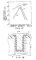
- FIG. 18 is a cross sectional view showing a semiconductor device manufactured by the conventional manufacturing method.
- An insulative film 2 is formed on the surface of a semiconductor wafer 1 and patterned.
- a trench 3 is formed in the semiconductor wafer 1 by etching the semiconductor wafer 1 with the insulative film 2 used as a mask.
- a single crystal Si layer doped with impurity that is, an impurity layer 4 is formed on the inner surface of the trench 3.
- the semiconductor wafer 1 is subjected to the cleaning process by use of chemicals.
- the semiconductor wafer 1 is loaded into a furnace (not shown).
- a CVD silicon nitride film 6 is deposited on the inner surface of the trench 3 and the insulative film 2 by the LPCVD (Low Pressure Chemical Vapor Deposition) method.
- a silicon oxide film 7 is formed on the silicon nitride film 6.
- a composite insulative film 9 formed of the silicon nitride film 6 and silicon oxide film 7 is formed in the trench 3.
- a polysilicon film 8a doped with impurity is deposited on the silicon oxide film 7.
- the internal portion of the trench 3 is filled with the polysilicon film 8a.
- a capacitor 10 is constructed by the electrode 10, the composite insulative film 9 and the insulative diffusion layer 4 used as an electrode in the trench 3.
- the silicon nitride film 6 When the silicon nitride film 6 is formed on the inner surface of the trench 3 in the furnace, a natural oxide film 5 with a thickness of approx. 1 nm to 2 nm is formed between the silicon nitride film 6 and the impurity diffusion layer 4. Therefore, the actual composite insulative film 9 is formed of the natural oxide film 5, silicon oxide film 7 and silicon nitride film 6.
- the cause of formation of the natural oxide film the following three causes are considered. The first cause is based on dissolved oxygen in the cleaning liquid in the cleaning process, the second cause is based on oxygen in the atmosphere, and the third cause is based on oxygen contained in the outside air introduced into the silicon nitride film forming furnace when the wafer 1 is carried into the furnace.
- the film thickness of the capacitor insulative film is increased by 1 nm to 2 nm, thereby preventing the film thickness of the capacitor insulative film from being reduced. Further, if the natural oxide film is formed, the film quality of the capacitor insulative film is deteriorated, thereby lowering the dielectric strength and degrading the reliability of the insulative film.
- a method of removing the natural oxide film 5 in the trench 3 by forming an atmosphere in which the partial pressures of H 2 0 and 0 2 are set equal to or lower than 1 x 10- 4 Torr in the furnace used for the LPCVD method, processing the semiconductor wafer 1 in the atmosphere, and then forming the CVD silicon nitride film 6 is considered.
- a method of reducing the natural oxide film 5 by introducing a reducing gas such as H 2 , SiH 4 , Si 2 He, and HCI into the furnace used for the LPCVD and then forming a thermal nitride film is considered.
- the clean inner surface of the trench 3 is exposed to the high-temperature and low-pressure atmosphere so that impurity in the impurity diffusion layer 4 will be diffused towards the outside and extracted.
- a composite insulative film formed by the above method is used for the capacitor insulative film of the memory cell and when an electric field is applied to the capacitor insulative film, the interface area between the capacitor insulative film and the impurity diffusion layer is depleted, thereby causing a problem that an effective storage amount of charges cannot be obtained.
- etching pits may be formed in the inner surface of the trench by an oxidation gas such as H 2 0 or 0 2 in some cases.
- SiC may be sometimes formed on the inner surface of the trench by a carbonaceous gas such as CO, C0 2 and hydro-carbon gas. Therefore, if a composite insulative film formed by the above methods is used for the capacitor insulative film of the memory cell, a problem that the dielectric strength and the reliability of the capacitor insulative film are lowered occurs.
- An object of this invention is to provide a semiconductor device which is high in the dielectric strength, can prevent degradation in the reliability, can be made thin and is suitable for a composite insulative film, and a method of manufacturing the same.
- the above object can be attained by a semi- conductor device comprising a semiconductor layer; and a thermal nitride film formed directly on the semiconductor layer, the concentration of oxygen contained in the thermal nitride film being not high- er than 1.36 x 1 0 15 (atoms/cm 2 ).
- a semiconductor device manufacturing method comprising a first step of removing a natural oxide film on a semiconductor layer, and substantially at the same time, forming a thermal nitride film on the semi-conductor layer; and a second step of forming a nitride film on the thermal nitride film by the CVD method.
- the thermal nitride film is formed directly on the semiconductor layer and the concentration of oxygen in the thermal nitride film is set to be not higher than 1.36 x 10 15 (atoms/cm 2 ). Therefore, the flatness of a silicon nitride film formed on the thermal nitride film can be enhanced and the dielectric strength can be prevented from being lowered. In addition, since no natural oxide film is formed between the thermal nitride film and the silicon nitride film, the film thickness can be made small.
- the thermal nitride film is formed on the semiconductor layer substantially at the same time that the natural oxide film formed on the substrate is removed. Therefore, the concentration of oxygen contained in the thermal nitride film can be set extremely low. Thus, since a silicon nitride film excellent in the flatness can be formed on the thermal nitride film, the dielectric strength and reliability can be prevented from being lowered and the film thickness can be made small. Further, the natural oxide film on the semiconductor layer can be unfailingly removed by setting the partial pressures of H 2 0 and 0 2 to be values shown in equation (1) to be described later.
- the thermal nitride film can be formed on the surface of the semiconductor layer at the same time as elimination of the natural oxide film by introducing ammonia gas of low pressure. After this, a natural oxide film can be prevented from being formed between the thermal nitride film and the silicon nitride film by forming the silicon nitride film following on the formation of the thermal nitride film.
- the insulative film thus formed is high in the insulation dielectric 5 strength and excellent in the reliability and can be formed thin.
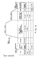
- FIG. 1 shows a high-vacuum LPCVD device used for manufacturing a semiconductor device by the manufacturing method of a first or second embodiment of this invention.
- An inner tube 12 formed of quartz is disposed inside an outer tube 11 which is formed of quartz and is closed at one end and the internal space of the inner tube 12 is used as a processing chamber 13.
- the outer tube 11 and inner tube 12 of the double-tube structure are supported by a SUS-made manifold 14 and one end of the manifold 14 and the other end of the outer tube 11 are hermetically sealed by an O-ring 16 or metal seal.
- a heater 24 for heating the internal portion of the processing chamber 13 is disposed outside the outer tube 11.
- An SUS-made capping flange 15 is mounted on the other end of the manifold 14 and the capping flange 15 and the other end of the manifold 14 are connected together by an O-ring 16 or metal seal.
- the processing chamber 13 is hermetically sealed.
- a quartz boat 23 which can carry a plurality of semiconductor wafers is disposed on the capping flange 15 in the processing chamber 13.
- NH 3 gas introducing nozzle 17, SiH 2 Cl 2 gas introducing nozzle 18 and inert gas introducing nozzle 19 for introducing NH 3 gas, SiH 2 Cl 2 gas and inert gas such as N 2 and Ar into the processing chamber 13 are formed in the manifold 14.
- T.M.P turbo-molecular pump
- a mechanical booster pump (M.B.P) 21 is connected to the turbo-molecular pump 20 and a dry pump (D.P) 22 is connected to the mechanical booster pump (M.B.P) 21.
- FIG. 2 shows the sequence of the semiconductor device manufacturing method according to the first or second embodiment of this invention.
- FIG. 3 is a cross sectional view showing a semiconductor device on which a composite insulative film constructed by three insulative films including a CVD silicon nitride film is formed as a capacitor insulative film of the memory cell.
- a semiconductor device manufacturing method according to the first embodiment of this invention is explained with reference to FIGS. 1 to 3.
- an insulative film 32 is formed on the surface of a semiconductor wafer 31 and selectively patterned.
- a trench 33 is formed in the semiconductor wafer 31 by etching the semi- conductor wafer 31 with the insulative film 32 used as a mask so as to expose single crystal Si on the inner surface of the trench 33.
- impurity is doped into the exposed single crystal Si and a single crystal Si layer doped with impurity, that is, an impurity diffusion layer 34 is formed in the inner surface area of the trench 33.
- the impurity diffusion layer 34 is used as an electrode of the capacitor.
- the cleaning process for removing impurities is effected by dipping the wafer 31 into a solution containing hydrochloric acid and hydrogen peroxide solution, for example.
- a natural oxide film (not shown) is formed on the inner surface of the trench 33.
- the semiconductor wafer 31 is processed according to the sequence shown in FIG. 2. That is, the semiconductor wafer 1 is placed on a quartz boat 23 and the quartz boat 23 is loaded into a processing chamber 13 of the high-vacuum LPCVD device of FIG. 1 in which the temperature is set in a low temperature range from the room temperature to approx. 600 ° C. At this time, a natural oxide film (not shown) with a thickness of approx. 1 nm to 2 nm is formed on the inner surface of the trench 33.
- Ar gas is introduced into the processing chamber 13 at the flow rate of 10 slm from the nozzle 19.
- the inert gas in the processing chamber 13 is discharged by the dry pump 22, mechanical booster pump 21 and turbo molecular pump 20 to lower the pressure in the processing chamber 13 to 10- 3 Torr or less.
- the partial pressures of H 2 0 and 0 2 are set to 1 x 10- 4 Torr or less. It is difficult to independently set the partial pressures of H 2 0 and 0 2 , and therefore, the partial pressure of H 2 0 may be set to 1 x 10- 4 Torr or less for convenience, for example.
- NH 3 gas is introduced into the processing chamber 13 at the flow rate of 1 to 5 slm from the nozzle 17 and the pressure is controlled to form a low-pressure atmosphere of 0.1 to 100 Torr in the processing chamber 13.
- the NH 3 gas is introduced into the processing chamber 13 and the semiconductor wafer 31 is heated by the heater 24 to set the temperature thereof to, for example, 800 °C to 1200°C with the low-pressure atmosphere kept unchanged. In this state, the semiconductor wafer 31 is kept at the temperature of 800 ° C to 1200 ° C for approx. 0 to 120 min.
- the natural oxide film formed on the inner surface of the trench 33 is vaporized and eliminated, and at the same time, a thermal nitride film with a thickness of 2 nm to 5 nm is formed on the inner surface of the trench 33.
- the reason why the natural oxide film in the trench 33 can be removed is that the partial pressures of H 2 0 and 0 2 are set to 1 x 10- 4 Torr or less. Further, the reason why the thermal nitride film 35 is formed on the inner surface of the trench 33 is that the NH 3 gas is introduced into the processing chamber 13 with the temperature of the wafer 31 kept at 800 ° C to 1200 ° C.
- FIG. 4 is a graph showing the relation between the partial pressures of H 2 0 and 0 2 in the processing chamber and the temperature.
- the concentration of oxygen in the thermal nitride film becomes less than 1.36 x 10 15 atoms/cm 2 (less than that of an oxygen monoatomic layer) and it is understood that the natural oxide film has been removed.
- the concentration of oxygen of the oxygen monoatomic layer formed on the silicon layer is 1.36 x 10 15 atoms/cm 2
- the concentration of oxygen of the natural oxide film formed on the silicon layer is at least more than the above value.
- the concentration of oxygen of the nitride film thermally formed without removing the natural oxide film is at least 1.36 x 10 15 atoms/cm 2 or more. Therefore, in the case where the concentration of oxygen of the thermal nitride film formed on the silicon layer is less than 1.36 x 10 15 atoms/cm 2 , the natural oxide film is removed to form the thermal nitride film.
- the partial pressures of H 2 0 and 0 2 to the temperature of the characteristics of FIG. 4 can be expressed by the following equation (1): where S: inclination (1 x 10 8 to 1 x 10 9 ), E: active energy (-2.5 to 3.5), C: coefficient for transferring Joule/mol to eV (11605), and T: absolute temperature.
- the partial pressures of H 2 0 and 0 2 are set to less than Pr obtained by the above equation (1), thereby the natural oxide film on the semiconductor layer can be removed without fail.
- an optimum temperature condition of processing is 800 to 900 °C, and the partial pressures H 2 0 and 0 2 are substantially 2.5 x 10- 5 to 3.5 x 10- 4 Torr.
- NH 3 gas is introduced into the processing chamber 13 when the temperature of the semiconductor wafer 31 is raised. Therefore, impurity will not be extracted from the impurity diffusion layer 34.
- the temperature of the wafer is lowered to 750 ° C to 600 ° C while NH 3 is being continuously introduced with the internal space of the processing chamber 13 kept in the low-pressure atmosphere.
- SiH 2 Cl 2 gas is introduced into the processing chamber 13 from the nozzle 18 at the flow rate of 0.1 slm and the flow rate of NH 3 introduced from the nozzle 17 is set to 1 slm to adjust the internal pressure of the processing chamber 13 to 0.5 Torr.
- a CVD silicon nitride film (which is hereinafter referred to as CVD-SiN film) is formed on the thermal nitride film 35 and insulative film 32.
- the temperature of the semiconductor wafer 31 is lowered to the room temperature to approx. 600 °C.
- introduction of SiH 2 CI 2 gas and NH 3 gas into the processing chamber 13 is interrupted and Ar gas is introduced into the processing chamber 13 from the nozzle 19 at the flow rate of approx. 5 slm.
- the pressure in the processing chamber 13 is adjusted to approx. 1 Torr.
- the semiconductor wafer 31 is taken out from the processing chamber 13.
- the semiconductor wafer 31 is carried into a furnace different from the LPCVD device shown in FIG. 1, and as shown in FIG. 3, a silicon oxide film 37 (CVD silicon oxide film or thermal silicon oxide film) with a thickness of approx. 1 nm to 2 nm is formed on the CVD-SiN film 36.
- a composite insulative film 38 of three-layered structure formed of the silicon oxide film 37, CVD-SiN film 36 and thermal nitride film 35 is formed.
- a polysilicon film 39a doped with impurity is deposited on the composite insulative film 38 and patterned together with the composite insulative film 38.
- an electrode 39 formed of the polysilicon film 39a is disposed in the trench 33. Therefore, in the trench 33, a capacitor 40 is constructed by the electrode 39, composite insulative film 38 and impurity diffusion layer 34.
- the partial pressures of H 2 0 and 0 2 in the processing chamber are set to be lower than the condition shown in equation (1), and the wafer 31 is processed in an atmosphere created by introducing NH 3 gas at the flow rate of 1 to 5 slm into the processing chamber 13.
- the natural oxide film on the inner surface of the trench 33 can be removed, and at the same time, the thermal nitride film 35 with a thickness of approx. 2 nm to 5 nm can be formed. Therefore, a natural oxide film will not be formed between the impurity diffusion layer 34 and the CVD-SiN film 36, thereby preventing the electrical characteristic of the composite insulative film 38 from being lowered and making it possible to form a thin film.
- the flatness of the surface of the natural oxide film is considerably bad.
- the nitride film is conventionally formed on the surface of the natural oxide film, the flatness of the surface naturally worsens. In such a bad flatness condition, electrical field concentrates on the thin portion of the nitride film, and leak current to cause the generation of leak current. Due to this, it is needed that the nitride film be formed thick.
- the thermal nitride film is directly formed on the silicon layer, good flatness can be obtained. As a result, the generation of leak current can be prevented, and the thermal nitride film can be formed thin.
- the thermal nitride film is directly formed on the silicon layer, no oxide film exists in the film, and the quality of the film can be stabilized. Therefore, the removal of the natural oxide film and the formation of the thermal nitride film 35 are performed at the same time, so that the thermal nitride film 35 can be thinned and prevented from being deteriorated at the same time.
- the concentration of oxygen in the surface of the thermal nitride film 35 can be lowered by forming the thermal nitride film 35 at the same time as elimination of the natural oxide film on the inner surface of the trench 33 and then forming the CVD-SiN film 36 on the thermal nitride film 35. Therefore, the formation delay time at the time of formation of the CVD-SiN film 36, that is, the incubation time can be reduced to zero. As a result, the morphology of the CVD-SiN film 36 can be made excellent and the roughness thereof becomes small, thereby enhancing the flatness of the surface thereof. Therefore, the leak current of the CVD-SiN film 36 becomes small and the dielectric strength can be prevented from being lowered.
- the concentration of oxygen in the thermal nitride film 35 can be kept at approx. 0.8 x 10 15 (atoms/cm 2 ) which is smaller than 1.36 x 10 15 (atoms/cm 2 ).
- the concentration of oxygen in the thermal nitride film 35 is low and when the CVD-SiN film 36 is formed on the thermal nitride film 35, the incubation time can be reduced to zero. Therefore, as shown in FIG. 5A, nucleus can be uniformly formed when the CVD-SiN film 36 is formed on the surface of the thermal nitride film.
- the concentration of oxygen in the thermal nitride film is set higher than 1.36 x 10 15 - (atoms/cm 2 ). Therefore, the incubation time cannot be set to zero when the CVD-SiN film is formed on the thermal nitride film, and as shown in FIG. 5C, non-uniform nucleus are formed on the surface of the thermal nitride film.
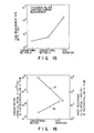
- FIG. 6 is a graph showing the relation between the incubation time and the concentration of oxygen contained in the ground film when the CVD-SiN film is formed.
- FIG. 6 indicates the results obtained by measuring the concentration of oxygen contained on the thermal nitride film by SIMS (Secondary Ion Mass Spectrometry) after forming the CVD-SiN film on the thermal nitride film on the silicon substrate with different incubation time. It is understood from FIG. 6 that the incubation time is set to zero when the concentration of oxygen in the ground layer is set equal to or lower than 1 x 10 15 (atoms/cm2) .
- FIG. 7 shows the relation between time for formation of the CVD-SiN film formed on the thermal nitride film with a film thickness of 20 angstrom and the total film thickness of the thermal nitride film and the CVD-SiN film.
- the line A indicates a case wherein the thermal nitride film and the CVD-SiN film are continuously formed and the concentration of oxygen contained in the thermal nitride film is 0.8 x 10 15 (atoms/cm 2 )
- the line B indicates a case wherein the thermal nitride film and the CVD-SiN film are continuously formed and the concentration of oxygen contained in the thermal nitride film is 1.5 x 10 15 (atoms/cm 2 )
- the line C indicates a case wherein the thermal nitride film and the CVD-SiN film are discontinuously formed, the surface of the thermal nitride film is oxidized, and the concentration of oxygen contained in the thermal nitride film is 1.8
- FIG. 8 shows the relation between the incubation time at the time of formation of the CVD-SiN film and the roughness of the surface of the CVD-SiN film formed.
- FIG. 8 shows the result of measurement of the film formed in the same manner as in the case of FIG. 6 by AFM. It is clearly understood from FIG. 8 that the roughness becomes larger as the incubation time becomes longer. That is, if the incubation time is zero, the CVD-SiN film is formed with the uniform film thickness as shown in FIG. 5B. Therefore, the surface of the CVD-SiN film is made flat. However, if the incubation time is long, the film thickness of the CVD-SiN film becomes non-uniform as shown in FIG.
- FIG. 9 shows the relation between the incubation time and the leak current density of the NO film
- FIG. 10 shows the relation between the incubation time and the dielectric breakdown of the NO film.
- FIG. 9 shows the result of measurement of the leak current density obtained when a voltage of ⁇ 1.65 V is applied between the semiconductor wafer and the Si0 2 film as shown in FIG. 11.
- FIG. 10 shows 50% MTTF (Mean Time To Failure) of the TDDB (Time Dependent Dielectric Breakdown) measurement by use of a constant current. 50% MTTF is the mean time until 50% of the measured samples are destroyed.
- TDDB Time Dependent Dielectric Breakdown
- the thickness of the composite insulative film is expressed in terms of the film thickness of the oxide film (the film thickness equivalent to the film thickness of the oxide film; thickness eq.) and is 45 angstrom in this example.
- the leak current density is lower and the dielectric strength becomes larger as the incubation time is shorter.
- FIG. 12 is a cross sectional view showing another semiconductor device on which a composite insulative film formed of three-layered insulative film including a CVD-SiN film is formed as a capacitor insulative film of the memory cell and portions which are the same as those of FIG. 3 are denoted by the same reference numerals.
- a semiconductor device manufacturing method according to the second embodiment of this invention is explained with reference to FIGS. 1, 2 and 5. Portions which are the same as those of the first embodiment are denoted by the same reference numerals and the explanation therefor is omitted.
- an oxide film 41 is formed on the inner side surface of the trench 33 of the semiconductor wafer 31.
- a single crystal Si film doped with impurity, that is, impurity diffusion layer 42 is formed on the bottom surface of the trench 33.
- a polysilicon film 43 is formed on the inner side surface and bottom surface of the trench 33 and impurity is doped into the polysilicon film 43.
- the semiconductor wafer 31 is subjected to the cleaning process.
- a natural oxide film (not shown) is formed on the surface of the polysilicon film 43.
- the semiconductor wafer 31 is processed according to the sequence shown in FIG. 2. That is, a thermal nitride film 35 is formed on the polysilicon film 43 in the furnace shown n FIG. 1. A CVD-SiN film 36 and silicon oxide film 37 are formed on the thermal nitride film 35. After this, a polysilicon film 39a doped with impurity is deposited on a composite insulative film 38 and an electrode 39 is formed inside the trench 33. Therefore, a capacitor 40 is formed of the electrode 39, composite insulative film 38 and polysilicon film 43 in the trench 33.
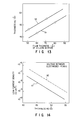
- FIG. 13 is a graph showing the relation between the film thickness of the silicon nitride film 36 and the film thickness of the composite insulative film 38 expressed in terms of the film thickness of the oxide film.
- a reference numeral 51 indicates the relation between the thickness of the nitride film in the composite insulative film of the semiconductor device manufactured by the manufacturing method of this invention and the effective film thickness equivalent to the film thickness of the oxide film obtained by electrically evaluating the thickness of the composite insulative film.
- a reference numeral 52 indicates the relation between the thickness of the nitride film in the composite insulative film of the semiconductor device manufactured by the conventional manufacturing method and the film thickness of the composite insulative film equivalent to the film thickness of the oxide film.
- the film thickness of the composite insulative film of this invention expressed in terms of the film thickness of the oxide film can be made thinner than that of the conventional case by approx. 7 angstrom if the silicon nitride film of the same thickness is used.
- the thermal nitride film having a large dielectric constant is used instead of the natural oxide film in this invention and the effective film thickness thereof equivalent to the film thickness of the oxide film can be increased. Therefore, the capacitor insulative film can be made thin and the capacitance can be increased by using the semiconductor device manufacturing method of this invention.
- FIG. 14 shows the relation between the film thickness of the composite insulative film expressed in terms of the film thickness of the oxide film and the leak current density.
- a reference numeral 61 indicates the relation between the film thickness of the composite insulative film expressed in terms of the film thickness of the oxide film in the semiconductor device manufactured by the manufacturing method of this invention and the leak current in the composite insulative film obtained when a voltage of ⁇ 1.65 V is applied to the electrode of the semiconductor device.
- a reference numeral 62 indicates the relation between the film thickness of the composite insulative film expressed in terms of the film thickness of the oxide film in the semiconductor device manufactured by the conventional manufacturing method and the leak current in the composite insulative film obtained when a voltage of ⁇ 1.65 V is applied to the electrode of the semiconductor device.
- the leak current density can be made lower in the composite insulative film of this invention than in the composite insulative film of the conventional case when they are compared by use of the same film thickness equivalent to the film thickness of the oxide film. This is because the natural oxide film which permits a large amount of electrical leak is formed on the composite insulative film formed by the conventional manufacturing method, but no natural oxide film is formed on the composite insulative film formed by the manufacturing method of this invention. Therefore, by using the semiconductor device manufacturing method of this invention, the leak current density can be reduced in comparison
- FIG. 15 shows the results of measurements of TDDB 50% MTTF obtained when a constant current of 1200 ⁇ A is passed in the composite insulative films manufactured by the manufacturing method of this invention and the conventional manufacturing method.
- the film thickness of the composite insulative film is set to 45 angstrom expressed in terms of the film thickness of the oxide film.
- the conventional method A indicates the result of TDDB measurement for a semiconductor device obtained by forming a thermal nitride film on the electrode of the semiconductor wafer in the first furnace used for LPCVD method, moving the semiconductor wafer from the first furnace into the second furnace, and forming a CVD-SiN film formed on the thermal nitride film in the second furnace.
- This invention indicates the result of TDDB measurement for a semiconductor device obtained by forming a thermal nitride film on the semiconductor wafer in the first furnace and continuously forming a CVD-SiN film formed on the thermal nitride film in the first furnace. That is, this invention indicates the result of TDDB measurement for a semiconductor device manufactured by the manufacturing method according to the first embodiment.
- the conventional method B indicates the result of TDDB measurement for a semiconductor device manufactured by the conventional manufacturing method.
- FIG. 16 shows the result of measurement of the concentration of impurity or P contained in a polysilicon film formed as a lower electrode of each of the semiconductor devices manufactured by the manufacturing method of this invention and the conventional manufacturing method and the sheet resistance of the polysilicon film.
- a reference numeral 81 indicates the result of measurement of the sheet resistance of the polysilicon film.
- a reference numeral 82 indicates the result of measurement of the concentration of P contained in the polysilicon film.
- a natural oxide film in the trench is removed by processing the semiconductor wafer in an atmosphere of reducing gas or by processing the semi- conductor wafer in an atmosphere of inert gas in which the partial pressures of H 2 0 and 0 2 are set to be low after the semiconductor wafer is subjected to the cleaning process, and then a thermal nitride film is formed in the trench.
- FIG. 17 shows the number of foreign matters on the wafer in a case where the semiconductor devices are manufactured by the manufacturing method of this invention and the conventional manufacturing method.
- the conventional method A indicates the number of foreign matters on the wafer in a case where the CVD-SiN film is formed without removing the natural oxide film on the electrode surface of the semiconductor wafer.
- the conventional method B indicates the number of foreign matters on the wafer in a case where the natural oxide film on the electrode surface of the semiconductor wafer is removed in an atmosphere of inert gas, a thermal nitride film is formed on the electrode surface by NH 3 gas, and then the CVD-SiN film is formed.
- this invention in FIG. 17 indicates the number of foreign matters on the wafer in a case where the CVD-SiN film is formed by the method of the first embodiment.
- a reference numeral 91 indicates the number of foreign matters with a diameter of 0.1 to 0.2 / .Lm and a reference numeral 92 indicates the number of foreign matters with a diameter of 0.2 / .Lm or more.
- the above process can be effected without increasing the number of foreign matters with a diameter of 0.1 /.Lm or more. Moreover, no etching pits are formed.
- this invention is not limited to this case, and it is possible to apply this invention to a capacitor with stack structure.
- the position where the thermal nitride film is formed is not limited to the surface of the semiconductor substrate.
- the thermal nitride film may be formed on the semiconductor layer formed on the semiconductor substrate.
- the above embodiments in which this invention is applied to the capacitor are explained, but this invention is not limited to this case, and it is possible to apply this invention to an oxidation- resistant mask for LOCOS. That is, the mask for LOCOS can be formed by continuously forming the thermal nitride film and CVD-silicon nitride film on the semi-conductor substrate by the above method and patterning the same. If the field oxidation is effected by use of this mask, occurrence of the birds beak in the field oxide film can be prevented.
- this invention is not limited to the semiconductor device using silicon but can be applied to a semiconductor device using GaAs.
Abstract
A semiconductor wafer (31) having an impurity diffusion layer formed in an inner surface of a trench (33) is cleaned. The semiconductor wafer (31) is inserted into a furnace, and NH3 gas is introduced into the furnace in the low-pressure condition to create an atmosphere in which the temperature is set at 800 °C to 1200°C and the partial pressures of H20 and 02 are set at 1 x 10⁻⁴ Torr or less. A natural oxide film formed on the inner surface of the trench (33) is removed, and substantially at the same time, a thermal nitride film (35) is formed on the impurity diffusion layer. Then, a CVD silicon nitride film (36) is formed on the thermal nitride film without exposing the thermal nitride film to the outside air in the same furnace. Next, a silicon oxide film (37) is formed on the CVD nitride film. As a result, a composite insulative film formed of the thermal nitride film, CVD silicon nitride film and silicon oxide film is obtained. Then, an electrode (39) for the composite insulative film is formed in the trench.
Description
- This invention relates to a semiconductor device and a manufacturing method thereof, and more particularly to formation of a composite insulative film by use of the CVD (Chemical Vapor Deposition) method.
- In a semiconductor integrated circuit, for example, an insulative film used for forming a capacitor of a memory cell is required to be made thin and have a large dielectric constant in order to stably provide a preset capacitance even when the size of the capacitor is reduced with an increase in the integration density. A silicon nitride film is known as an insulative film having a dielectric constant larger than that of a silicon oxide film.
- FIG. 18 is a cross sectional view showing a semiconductor device manufactured by the conventional manufacturing method. An
insulative film 2 is formed on the surface of asemiconductor wafer 1 and patterned. Atrench 3 is formed in thesemiconductor wafer 1 by etching thesemiconductor wafer 1 with theinsulative film 2 used as a mask. Next, a single crystal Si layer doped with impurity, that is, animpurity layer 4 is formed on the inner surface of thetrench 3. After this, thesemiconductor wafer 1 is subjected to the cleaning process by use of chemicals. - Next, the
semiconductor wafer 1 is loaded into a furnace (not shown). In the furnace, a CVDsilicon nitride film 6 is deposited on the inner surface of thetrench 3 and theinsulative film 2 by the LPCVD (Low Pressure Chemical Vapor Deposition) method. Next, asilicon oxide film 7 is formed on thesilicon nitride film 6. As a result, a compositeinsulative film 9 formed of thesilicon nitride film 6 andsilicon oxide film 7 is formed in thetrench 3. After this, a polysilicon film 8a doped with impurity is deposited on thesilicon oxide film 7. The internal portion of thetrench 3 is filled with the polysilicon film 8a. Next, the polysilicon film 8a,silicon oxide film 7 andsilicon nitride film 6 are patterned to form anelectrode 8 of the polysilicon film 8a in thetrench 3. Therefore, acapacitor 10 is constructed by theelectrode 10, the compositeinsulative film 9 and theinsulative diffusion layer 4 used as an electrode in thetrench 3. - When the
silicon nitride film 6 is formed on the inner surface of thetrench 3 in the furnace, anatural oxide film 5 with a thickness of approx. 1 nm to 2 nm is formed between thesilicon nitride film 6 and theimpurity diffusion layer 4. Therefore, the actual compositeinsulative film 9 is formed of thenatural oxide film 5,silicon oxide film 7 andsilicon nitride film 6. As the cause of formation of the natural oxide film, the following three causes are considered. The first cause is based on dissolved oxygen in the cleaning liquid in the cleaning process, the second cause is based on oxygen in the atmosphere, and the third cause is based on oxygen contained in the outside air introduced into the silicon nitride film forming furnace when thewafer 1 is carried into the furnace. - Thus, if the
natural oxide film 5 with a thickness of approx. 1 nm to 2 nm is formed between thesilicon nitride film 6 and theimpurity diffusion layer 4, the film thickness of the capacitor insulative film is increased by 1 nm to 2 nm, thereby preventing the film thickness of the capacitor insulative film from being reduced. Further, if the natural oxide film is formed, the film quality of the capacitor insulative film is deteriorated, thereby lowering the dielectric strength and degrading the reliability of the insulative film. - As a method of solving the above problems, a method of removing the
natural oxide film 5 in thetrench 3 by forming an atmosphere in which the partial pressures ofH semiconductor wafer 1 in the atmosphere, and then forming the CVDsilicon nitride film 6 is considered. - Further, a method of reducing the
natural oxide film 5 by introducing a reducing gas such as H2, SiH4, Si2He, and HCI into the furnace used for the LPCVD and then forming a thermal nitride film is considered. - However, according to the above two methods, after the
natural oxide film 5 on the inner wall of the trench is removed in the furnace, the clean inner surface of thetrench 3 is exposed to the high-temperature and low-pressure atmosphere so that impurity in theimpurity diffusion layer 4 will be diffused towards the outside and extracted. As a result, if a composite insulative film formed by the above method is used for the capacitor insulative film of the memory cell and when an electric field is applied to the capacitor insulative film, the interface area between the capacitor insulative film and the impurity diffusion layer is depleted, thereby causing a problem that an effective storage amount of charges cannot be obtained. - Further, according to the above two methods, since the clean inner surface of the
trench 3 is exposed to the high-temperature and low-pressure atmosphere after thenatural oxide film 5 in the trench is removed in the furnace, etching pits may be formed in the inner surface of the trench by an oxidation gas such asH - An object of this invention is to provide a semiconductor device which is high in the dielectric strength, can prevent degradation in the reliability, can be made thin and is suitable for a composite insulative film, and a method of manufacturing the same.
- The above object can be attained by a semi- conductor device comprising a semiconductor layer; and a thermal nitride film formed directly on the semiconductor layer, the concentration of oxygen contained in the thermal nitride film being not high- er than 1.36 x 10¹⁵ (atoms/cm2).
- Further, the above object can be attained by a semiconductor device manufacturing method comprising a first step of removing a natural oxide film on a semiconductor layer, and substantially at the same time, forming a thermal nitride film on the semi-conductor layer; and a second step of forming a nitride film on the thermal nitride film by the CVD method.
- According to the semiconductor device of this invention, the thermal nitride film is formed directly on the semiconductor layer and the concentration of oxygen in the thermal nitride film is set to be not higher than 1.36 x 10¹⁵ (atoms/cm2). Therefore, the flatness of a silicon nitride film formed on the thermal nitride film can be enhanced and the dielectric strength can be prevented from being lowered. In addition, since no natural oxide film is formed between the thermal nitride film and the silicon nitride film, the film thickness can be made small.
- According to the semiconductor device manufacturing method of this invention, the thermal nitride film is formed on the semiconductor layer substantially at the same time that the natural oxide film formed on the substrate is removed. Therefore, the concentration of oxygen contained in the thermal nitride film can be set extremely low. Thus, since a silicon nitride film excellent in the flatness can be formed on the thermal nitride film, the dielectric strength and reliability can be prevented from being lowered and the film thickness can be made small. Further, the natural oxide film on the semiconductor layer can be unfailingly removed by setting the partial pressures of
H - This invention can be more fully understood from the following detailed description when taken in conjunction with the accompanying drawings, in which:
- FIG. 1 is a construction view showing a high-vacuum LPCVD device used for manufacturing a semiconductor device by the manufacturing method of a first or second embodiment of this invention;
- FIG. 2 is a diagram showing the sequence of the semiconductor device manufacturing method according to the first or second embodiment of this invention;
- FIG. 3 is a cross sectional view showing a semiconductor device manufactured by a manufacturing method according to the first embodiment of this invention;
- FIG. 4 is a graph showing the relation between the partial pressures of
H - FIGS. 5A and 5B are diagrams for illustrating the CVD-SiN film and incubation time relating to the semiconductor device manufacturing method of this invention, and FIGS. 5C, 5D are diagrams for illustrating the CVD-SiN film and incubation time relating to the conventional semiconductor device manufacturing method;
- FIG. 6 is a graph showing the relation between the incubation time and the concentration of oxygen contained in the ground layer when the CVD-SiN film is formed;
- FIG. 7 is a graph showing the relation between time for forming the CVD-SiN film and the total film thickness of the thermal nitride film and the CVD-SiN film;
- FIG. 8 is a graph showing the relation between the incubation time at the time of formation of the CVD-SiN film and the roughness of the surface of the CVD-SiN film formed;
- FIG. 9 is a graph showing the relation between the incubation time and the leak current density of the NO film;
- FIG. 10 is a graph showing the relation between the incubation time and the genuine breakdown of the NO film;
- FIG. 11 is a view showing the structure of a sample used for FIGS. 9 and 10;
- FIG. 12 is a cross sectional view showing a semiconductor device manufactured by a manufacturing method according to the second embodiment of this invention;
- FIG. 13 is a graph showing the relation between the film thickness of the silicon nitride film and the film thickness expressed in terms of the film thickness of the oxide film;
- FIG. 14 is a graph showing the relation between the film thickness expressed in terms of the film thickness of the oxide film and the leak current density;
- FIG. 15 is a graph showing the results of TDDB measurements of the semiconductor devices manufactured by the manufacturing method of this invention and the conventional manufacturing method;
- FIG. 16 is a graph showing the sheet resistance of the polysilicon film and the impurity concentration of the polysilicon film of the semiconductor devices manufactured by the manufacturing method of this invention and the conventional manufacturing method;
- FIG. 17 is a graph showing the number of foreign matters on the wafer in a case where the semiconductor devices are manufactured by the manufacturing method of this invention and the conventional manufacturing method; and
- FIG. 18 is a cross sectional diagram showing a semiconductor device manufactured by the conventional manufacturing method.
- There will now be described an embodiment of this invention with reference to the accompanying drawings.
- FIG. 1 shows a high-vacuum LPCVD device used for manufacturing a semiconductor device by the manufacturing method of a first or second embodiment of this invention. An
inner tube 12 formed of quartz is disposed inside anouter tube 11 which is formed of quartz and is closed at one end and the internal space of theinner tube 12 is used as aprocessing chamber 13. Theouter tube 11 andinner tube 12 of the double-tube structure are supported by a SUS-mademanifold 14 and one end of the manifold 14 and the other end of theouter tube 11 are hermetically sealed by an O-ring 16 or metal seal. Aheater 24 for heating the internal portion of theprocessing chamber 13 is disposed outside theouter tube 11. - An SUS-made
capping flange 15 is mounted on the other end of the manifold 14 and the cappingflange 15 and the other end of the manifold 14 are connected together by an O-ring 16 or metal seal. Thus, theprocessing chamber 13 is hermetically sealed. Aquartz boat 23 which can carry a plurality of semiconductor wafers is disposed on the cappingflange 15 in theprocessing chamber 13. - An NH3
gas introducing nozzle 17, SiH2Cl2gas introducing nozzle 18 and inertgas introducing nozzle 19 for introducing NH3 gas, SiH2Cl2 gas and inert gas such as N2 and Ar into theprocessing chamber 13 are formed in themanifold 14. In FIG. 1, each of the nozzles is simply shown by an arrow. Further, a turbo-molecular pump (T.M.P) 20 for exhausting an internal gas in the processing chamber is connected to themanifold 14. A mechanical booster pump (M.B.P) 21 is connected to the turbo-molecular pump 20 and a dry pump (D.P) 22 is connected to the mechanical booster pump (M.B.P) 21. - FIG. 2 shows the sequence of the semiconductor device manufacturing method according to the first or second embodiment of this invention. FIG. 3 is a cross sectional view showing a semiconductor device on which a composite insulative film constructed by three insulative films including a CVD silicon nitride film is formed as a capacitor insulative film of the memory cell. Next, a semiconductor device manufacturing method according to the first embodiment of this invention is explained with reference to FIGS. 1 to 3.
- First, as shown in FIG. 3, an
insulative film 32 is formed on the surface of asemiconductor wafer 31 and selectively patterned. Atrench 33 is formed in thesemiconductor wafer 31 by etching the semi-conductor wafer 31 with theinsulative film 32 used as a mask so as to expose single crystal Si on the inner surface of thetrench 33. Next, impurity is doped into the exposed single crystal Si and a single crystal Si layer doped with impurity, that is, animpurity diffusion layer 34 is formed in the inner surface area of thetrench 33. Theimpurity diffusion layer 34 is used as an electrode of the capacitor. After this, thesemiconductor wafer 1 is subjected to the cleaning process by use of chemicals (not shown). Specifically, the cleaning process for removing impurities is effected by dipping thewafer 31 into a solution containing hydrochloric acid and hydrogen peroxide solution, for example. At the time of or after the cleaning process, a natural oxide film (not shown) is formed on the inner surface of thetrench 33. - Next, the
semiconductor wafer 31 is processed according to the sequence shown in FIG. 2. That is, thesemiconductor wafer 1 is placed on aquartz boat 23 and thequartz boat 23 is loaded into aprocessing chamber 13 of the high-vacuum LPCVD device of FIG. 1 in which the temperature is set in a low temperature range from the room temperature to approx. 600 ° C. At this time, a natural oxide film (not shown) with a thickness of approx. 1 nm to 2 nm is formed on the inner surface of thetrench 33. When thequartz boat 23 is carried into theprocessing chamber 13, Ar gas is introduced into theprocessing chamber 13 at the flow rate of 10 slm from thenozzle 19. After this, the inert gas in theprocessing chamber 13 is discharged by thedry pump 22,mechanical booster pump 21 and turbomolecular pump 20 to lower the pressure in theprocessing chamber 13 to 10-3 Torr or less. At this time, the partial pressures ofH H H 20 may be set to 1 x 10⁻⁴ Torr or less for convenience, for example. - After this, NH3 gas is introduced into the
processing chamber 13 at the flow rate of 1 to 5 slm from thenozzle 17 and the pressure is controlled to form a low-pressure atmosphere of 0.1 to 100 Torr in theprocessing chamber 13. Next, theNH 3 gas is introduced into theprocessing chamber 13 and thesemiconductor wafer 31 is heated by theheater 24 to set the temperature thereof to, for example, 800 °C to 1200°C with the low-pressure atmosphere kept unchanged. In this state, thesemiconductor wafer 31 is kept at the temperature of 800 ° C to 1200 ° C for approx. 0 to 120 min. As a result, the natural oxide film formed on the inner surface of thetrench 33 is vaporized and eliminated, and at the same time, a thermal nitride film with a thickness of 2 nm to 5 nm is formed on the inner surface of thetrench 33. - The reason why the natural oxide film in the
trench 33 can be removed is that the partial pressures ofH thermal nitride film 35 is formed on the inner surface of thetrench 33 is that the NH3 gas is introduced into theprocessing chamber 13 with the temperature of thewafer 31 kept at 800 ° C to 1200 ° C. - FIG. 4 is a graph showing the relation between the partial pressures of
H H - Since the concentration of oxygen of the oxygen monoatomic layer formed on the silicon layer is 1.36 x 10¹⁵ atoms/cm2, the concentration of oxygen of the natural oxide film formed on the silicon layer is at least more than the above value. Generally, in the case where the thermal nitride film is formed on the silicon oxide film, the formed thermal nitride film takes in oxygen of the silicon oxide film. Due to this, the concentration of oxygen of the nitride film thermally formed without removing the natural oxide film is at least 1.36 x 10¹⁵ atoms/cm2 or more. Therefore, in the case where the concentration of oxygen of the thermal nitride film formed on the silicon layer is less than 1.36 x 10¹⁵ atoms/cm2, the natural oxide film is removed to form the thermal nitride film.
- The partial pressures of
H 
- The partial pressures of
H partial pressures H - NH3 gas is introduced into the
processing chamber 13 when the temperature of thesemiconductor wafer 31 is raised. Therefore, impurity will not be extracted from theimpurity diffusion layer 34. - Next, the temperature of the wafer is lowered to 750 ° C to 600 ° C while NH3 is being continuously introduced with the internal space of the
processing chamber 13 kept in the low-pressure atmosphere. After this, SiH2Cl2 gas is introduced into theprocessing chamber 13 from thenozzle 18 at the flow rate of 0.1 slm and the flow rate of NH3 introduced from thenozzle 17 is set to 1 slm to adjust the internal pressure of theprocessing chamber 13 to 0.5 Torr. Thus, as shown in FIG. 3, a CVD silicon nitride film (which is hereinafter referred to as CVD-SiN film) is formed on thethermal nitride film 35 andinsulative film 32. - After this, the temperature of the
semiconductor wafer 31 is lowered to the room temperature to approx. 600 °C. At this time, introduction of SiH2CI2 gas and NH3 gas into theprocessing chamber 13 is interrupted and Ar gas is introduced into theprocessing chamber 13 from thenozzle 19 at the flow rate of approx. 5 slm. At this time, the pressure in theprocessing chamber 13 is adjusted to approx. 1 Torr. - Next, after gases in the
processing chamber 13 are replaced by Ar gas, thesemiconductor wafer 31 is taken out from theprocessing chamber 13. - After this, the
semiconductor wafer 31 is carried into a furnace different from the LPCVD device shown in FIG. 1, and as shown in FIG. 3, a silicon oxide film 37 (CVD silicon oxide film or thermal silicon oxide film) with a thickness of approx. 1 nm to 2 nm is formed on the CVD-SiN film 36. As a result, acomposite insulative film 38 of three-layered structure formed of thesilicon oxide film 37, CVD-SiN film 36 andthermal nitride film 35 is formed. Next, a polysilicon film 39a doped with impurity is deposited on thecomposite insulative film 38 and patterned together with thecomposite insulative film 38. Thus, an electrode 39 formed of the polysilicon film 39a is disposed in thetrench 33. Therefore, in thetrench 33, acapacitor 40 is constructed by the electrode 39,composite insulative film 38 andimpurity diffusion layer 34. - According to the first embodiment, the partial pressures of
H wafer 31 is processed in an atmosphere created by introducing NH3 gas at the flow rate of 1 to 5 slm into theprocessing chamber 13. As a result, the natural oxide film on the inner surface of thetrench 33 can be removed, and at the same time, thethermal nitride film 35 with a thickness of approx. 2 nm to 5 nm can be formed. Therefore, a natural oxide film will not be formed between theimpurity diffusion layer 34 and the CVD-SiN film 36, thereby preventing the electrical characteristic of thecomposite insulative film 38 from being lowered and making it possible to form a thin film. - Also, the flatness of the surface of the natural oxide film is considerably bad. In the case that the nitride film is conventionally formed on the surface of the natural oxide film, the flatness of the surface naturally worsens. In such a bad flatness condition, electrical field concentrates on the thin portion of the nitride film, and leak current to cause the generation of leak current. Due to this, it is needed that the nitride film be formed thick. However, in the present invention, since the thermal nitride film is directly formed on the silicon layer, good flatness can be obtained. As a result, the generation of leak current can be prevented, and the thermal nitride film can be formed thin. Moreover, since the thermal nitride film is directly formed on the silicon layer, no oxide film exists in the film, and the quality of the film can be stabilized. Therefore, the removal of the natural oxide film and the formation of the
thermal nitride film 35 are performed at the same time, so that thethermal nitride film 35 can be thinned and prevented from being deteriorated at the same time. - Further, the concentration of oxygen in the surface of the
thermal nitride film 35 can be lowered by forming thethermal nitride film 35 at the same time as elimination of the natural oxide film on the inner surface of thetrench 33 and then forming the CVD-SiN film 36 on thethermal nitride film 35. Therefore, the formation delay time at the time of formation of the CVD-SiN film 36, that is, the incubation time can be reduced to zero. As a result, the morphology of the CVD-SiN film 36 can be made excellent and the roughness thereof becomes small, thereby enhancing the flatness of the surface thereof. Therefore, the leak current of the CVD-SiN film 36 becomes small and the dielectric strength can be prevented from being lowered. - Further, at the time of raise of the temperature of the
semiconductor wafer 31, and at the time of elimination of the natural oxide film on the inner surface of thetrench 33 and formation of thethermal nitride film 35, NH3 gas is introduced intoprocessing chamber 13 and the above processes are continuously effected. Therefore, unlike the conventional technique in which the thermal nitride film is formed after the natural oxide film in the trench is removed, impurity in the impurity diffusion layer is not extracted and occurrence of etching pits can be prevented. - Next, the above effect is explained in detail.
- In a case where the natural oxide film on the inner surface of the trench 33 (semiconductor wafer) is removed, and at the same time, the
thermal nitride film 35 is formed on the inner surface of thetrench 33, and then the CVD-SiN film 36 is continuously formed on thethermal nitride film 35, the concentration of oxygen in thethermal nitride film 35 can be kept at approx. 0.8 x 10¹⁵ (atoms/cm2) which is smaller than 1.36 x 10¹⁵ (atoms/cm2). Thus, if the concentration of oxygen in thethermal nitride film 35 is low and when the CVD-SiN film 36 is formed on thethermal nitride film 35, the incubation time can be reduced to zero. Therefore, as shown in FIG. 5A, nucleus can be uniformly formed when the CVD-SiN film 36 is formed on the surface of the thermal nitride film. - On the other hand, in a case where the natural oxide film on the inner surface of the trench is not sufficiently eliminated, and the processes for forming the thermal nitride film and the CVD-SiN film are discontinuously effected like the conventional case, the concentration of oxygen in the thermal nitride film is set higher than 1.36 x 10¹⁵ - (atoms/cm2). Therefore, the incubation time cannot be set to zero when the CVD-SiN film is formed on the thermal nitride film, and as shown in FIG. 5C, non-uniform nucleus are formed on the surface of the thermal nitride film.
- FIG. 6 is a graph showing the relation between the incubation time and the concentration of oxygen contained in the ground film when the CVD-SiN film is formed. FIG. 6 indicates the results obtained by measuring the concentration of oxygen contained on the thermal nitride film by SIMS (Secondary Ion Mass Spectrometry) after forming the CVD-SiN film on the thermal nitride film on the silicon substrate with different incubation time. It is understood from FIG. 6 that the incubation time is set to zero when the concentration of oxygen in the ground layer is set equal to or lower than 1 x 10¹⁵ (atoms/cm2).
- FIG. 7 shows the relation between time for formation of the CVD-SiN film formed on the thermal nitride film with a film thickness of 20 angstrom and the total film thickness of the thermal nitride film and the CVD-SiN film. In this example, the line A indicates a case wherein the thermal nitride film and the CVD-SiN film are continuously formed and the concentration of oxygen contained in the thermal nitride film is 0.8 x 10¹⁵ (atoms/cm2), the line B indicates a case wherein the thermal nitride film and the CVD-SiN film are continuously formed and the concentration of oxygen contained in the thermal nitride film is 1.5 x 10¹⁵ (atoms/cm2), and the line C indicates a case wherein the thermal nitride film and the CVD-SiN film are discontinuously formed, the surface of the thermal nitride film is oxidized, and the concentration of oxygen contained in the thermal nitride film is 1.8 x 10¹⁵ - (atoms/cm2). It is clearly understood from FIG. 7 that as the concentration of oxygen in the thermal nitride film becomes higher, delay of the film formation is generated, the incubation time becomes longer and the total film thickness is made smaller if the film formation time is the same. As mentioned above, in the case where the concentration of oxygen contained in the thermal nitride film is high and the thermal nitride film and the CVD-SiN film are discontinuously formed, incubation time for several minutes is generated.
- FIG. 8 shows the relation between the incubation time at the time of formation of the CVD-SiN film and the roughness of the surface of the CVD-SiN film formed. FIG. 8 shows the result of measurement of the film formed in the same manner as in the case of FIG. 6 by AFM. It is clearly understood from FIG. 8 that the roughness becomes larger as the incubation time becomes longer. That is, if the incubation time is zero, the CVD-SiN film is formed with the uniform film thickness as shown in FIG. 5B. Therefore, the surface of the CVD-SiN film is made flat. However, if the incubation time is long, the film thickness of the CVD-SiN film becomes non-uniform as shown in FIG. 5D and it is considered that the roughness of the surface of the CVD-SiN film becomes larger. If the roughness of the surface of the CVD-SiN film thus becomes larger, a leak path is formed in a portion with a small film thickness and the dielectric strength is degraded.
- FIG. 9 shows the relation between the incubation time and the leak current density of the NO film, and FIG. 10 shows the relation between the incubation time and the dielectric breakdown of the NO film. In the case of FIGS. 9 and 10, a composite film with a structure shown in FIG. 11 and formed with different incubation time is used. FIG. 9 shows the result of measurement of the leak current density obtained when a voltage of ±1.65 V is applied between the semiconductor wafer and the Si02 film as shown in FIG. 11. FIG. 10 shows 50% MTTF (Mean Time To Failure) of the TDDB (Time Dependent Dielectric Breakdown) measurement by use of a constant current. 50% MTTF is the mean time until 50% of the measured samples are destroyed. In FIGS. 9 and 10, the thickness of the composite insulative film is expressed in terms of the film thickness of the oxide film (the film thickness equivalent to the film thickness of the oxide film; thickness eq.) and is 45 angstrom in this example. As is clearly understood from FIGS. 9 and 10, the leak current density is lower and the dielectric strength becomes larger as the incubation time is shorter.
- FIG. 12 is a cross sectional view showing another semiconductor device on which a composite insulative film formed of three-layered insulative film including a CVD-SiN film is formed as a capacitor insulative film of the memory cell and portions which are the same as those of FIG. 3 are denoted by the same reference numerals. Next, a semiconductor device manufacturing method according to the second embodiment of this invention is explained with reference to FIGS. 1, 2 and 5. Portions which are the same as those of the first embodiment are denoted by the same reference numerals and the explanation therefor is omitted.
- As shown in FIG. 12, an
oxide film 41 is formed on the inner side surface of thetrench 33 of thesemiconductor wafer 31. After this, a single crystal Si film doped with impurity, that is,impurity diffusion layer 42 is formed on the bottom surface of thetrench 33. Next, apolysilicon film 43 is formed on the inner side surface and bottom surface of thetrench 33 and impurity is doped into thepolysilicon film 43. After this, thesemiconductor wafer 31 is subjected to the cleaning process. At this time, a natural oxide film (not shown) is formed on the surface of thepolysilicon film 43. - Next, the
semiconductor wafer 31 is processed according to the sequence shown in FIG. 2. That is, athermal nitride film 35 is formed on thepolysilicon film 43 in the furnace shown n FIG. 1. A CVD-SiN film 36 andsilicon oxide film 37 are formed on thethermal nitride film 35. After this, a polysilicon film 39a doped with impurity is deposited on acomposite insulative film 38 and an electrode 39 is formed inside thetrench 33. Therefore, acapacitor 40 is formed of the electrode 39,composite insulative film 38 andpolysilicon film 43 in thetrench 33. - The same effect obtained in the first embodiment can be attained in the second embodiment.
- FIG. 13 is a graph showing the relation between the film thickness of the
silicon nitride film 36 and the film thickness of thecomposite insulative film 38 expressed in terms of the film thickness of the oxide film. Areference numeral 51 indicates the relation between the thickness of the nitride film in the composite insulative film of the semiconductor device manufactured by the manufacturing method of this invention and the effective film thickness equivalent to the film thickness of the oxide film obtained by electrically evaluating the thickness of the composite insulative film. Areference numeral 52 indicates the relation between the thickness of the nitride film in the composite insulative film of the semiconductor device manufactured by the conventional manufacturing method and the film thickness of the composite insulative film equivalent to the film thickness of the oxide film. - It is understood from FIG. 13 that the film thickness of the composite insulative film of this invention expressed in terms of the film thickness of the oxide film can be made thinner than that of the conventional case by approx. 7 angstrom if the silicon nitride film of the same thickness is used. This is because the thermal nitride film having a large dielectric constant is used instead of the natural oxide film in this invention and the effective film thickness thereof equivalent to the film thickness of the oxide film can be increased. Therefore, the capacitor insulative film can be made thin and the capacitance can be increased by using the semiconductor device manufacturing method of this invention.
- FIG. 14 shows the relation between the film thickness of the composite insulative film expressed in terms of the film thickness of the oxide film and the leak current density. A
reference numeral 61 indicates the relation between the film thickness of the composite insulative film expressed in terms of the film thickness of the oxide film in the semiconductor device manufactured by the manufacturing method of this invention and the leak current in the composite insulative film obtained when a voltage of ±1.65 V is applied to the electrode of the semiconductor device. Areference numeral 62 indicates the relation between the film thickness of the composite insulative film expressed in terms of the film thickness of the oxide film in the semiconductor device manufactured by the conventional manufacturing method and the leak current in the composite insulative film obtained when a voltage of ±1.65 V is applied to the electrode of the semiconductor device. - It is understood from FIG. 14 that the leak current density can be made lower in the composite insulative film of this invention than in the composite insulative film of the conventional case when they are compared by use of the same film thickness equivalent to the film thickness of the oxide film. This is because the natural oxide film which permits a large amount of electrical leak is formed on the composite insulative film formed by the conventional manufacturing method, but no natural oxide film is formed on the composite insulative film formed by the manufacturing method of this invention. Therefore, by using the semiconductor device manufacturing method of this invention, the leak current density can be reduced in comparison
- with that in the conventional case and the dielectric strength and the reliability of the composite insulative film can be enhanced.
- FIG. 15 shows the results of measurements of TDDB 50% MTTF obtained when a constant current of 1200 µA is passed in the composite insulative films manufactured by the manufacturing method of this invention and the conventional manufacturing method. In this case, it is assumed that the film thickness of the composite insulative film is set to 45 angstrom expressed in terms of the film thickness of the oxide film.
- In FIG. 15, the conventional method A indicates the result of TDDB measurement for a semiconductor device obtained by forming a thermal nitride film on the electrode of the semiconductor wafer in the first furnace used for LPCVD method, moving the semiconductor wafer from the first furnace into the second furnace, and forming a CVD-SiN film formed on the thermal nitride film in the second furnace. This invention indicates the result of TDDB measurement for a semiconductor device obtained by forming a thermal nitride film on the semiconductor wafer in the first furnace and continuously forming a CVD-SiN film formed on the thermal nitride film in the first furnace. That is, this invention indicates the result of TDDB measurement for a semiconductor device manufactured by the manufacturing method according to the first embodiment. In FIG. 15, the conventional method B indicates the result of TDDB measurement for a semiconductor device manufactured by the conventional manufacturing method.
- As is clearly seen from FIG. 15, when the thermal nitride film and CVD-SiN film are continuously formed in the same furnace without being exposed to the outer atmosphere as in this invention, the reliability which is approx. 50 times higher than that obtained by the conventional method can be attained.
- FIG. 16 shows the result of measurement of the concentration of impurity or P contained in a polysilicon film formed as a lower electrode of each of the semiconductor devices manufactured by the manufacturing method of this invention and the conventional manufacturing method and the sheet resistance of the polysilicon film. A
reference numeral 81 indicates the result of measurement of the sheet resistance of the polysilicon film. Areference numeral 82 indicates the result of measurement of the concentration of P contained in the polysilicon film. - In the conventional manufacturing method, a natural oxide film in the trench is removed by processing the semiconductor wafer in an atmosphere of reducing gas or by processing the semi- conductor wafer in an atmosphere of inert gas in which the partial pressures of
H - As is clearly seen from FIG. 16, in the conventional manufacturing method, impurity in the polysilicon film is extracted when the thermal nitride film is formed on the polysilicon film. On the other hand, in the manufacturing method of this invention, since NH3 gas is introduced into the furnace from the time when the temperature of the semi- conductor wafer is raised until the CVD-SiN film is formed, impurity in the polysilicon film will not be extracted. Also, a natural oxide film on the polysilicon film is removed and the thermal nitride film can be formed thereon at the same time. FIG. 17 shows the number of foreign matters on the wafer in a case where the semiconductor devices are manufactured by the manufacturing method of this invention and the conventional manufacturing method. In FIG. 17, the conventional method A indicates the number of foreign matters on the wafer in a case where the CVD-SiN film is formed without removing the natural oxide film on the electrode surface of the semiconductor wafer. The conventional method B indicates the number of foreign matters on the wafer in a case where the natural oxide film on the electrode surface of the semiconductor wafer is removed in an atmosphere of inert gas, a thermal nitride film is formed on the electrode surface by NH3 gas, and then the CVD-SiN film is formed. Further, this invention in FIG. 17 indicates the number of foreign matters on the wafer in a case where the CVD-SiN film is formed by the method of the first embodiment. A
reference numeral 91 indicates the number of foreign matters with a diameter of 0.1 to 0.2 /.Lm and areference numeral 92 indicates the number of foreign matters with a diameter of 0.2 /.Lm or more. - According to the case of FIG. 17, in the manufacturing method of the first embodiment, the above process can be effected without increasing the number of foreign matters with a diameter of 0.1 /.Lm or more. Moreover, no etching pits are formed.
- The embodiment in which this invention is applied to the capacitor of trench structure is explained, but this invention is not limited to this case, and it is possible to apply this invention to a capacitor with stack structure. Also, the position where the thermal nitride film is formed is not limited to the surface of the semiconductor substrate. The thermal nitride film may be formed on the semiconductor layer formed on the semiconductor substrate.
- Further, the above embodiments in which this invention is applied to the capacitor are explained, but this invention is not limited to this case, and it is possible to apply this invention to an oxidation- resistant mask for LOCOS. That is, the mask for LOCOS can be formed by continuously forming the thermal nitride film and CVD-silicon nitride film on the semi-conductor substrate by the above method and patterning the same. If the field oxidation is effected by use of this mask, occurrence of the birds beak in the field oxide film can be prevented.
- Further, this invention is not limited to the semiconductor device using silicon but can be applied to a semiconductor device using GaAs.
Claims (19)
1. A semiconductor device characterized by comprising a semiconductor layer (34); and a thermal nitride film (35) formed directly on said semiconductor layer, the concentration of oxygen contained in said thermal nitride film being not higher than 1.36 x 10¹⁵ (atoms/cm2).
2. A device according to claim 1, characterized in that said semiconductor layer (34) is formed of silicon.
3. A device according to claim 2, characterized by further comprising a CVD-silicon nitride film (36) formed on said thermal nitride film.
4. A device according to claim 3, characterized by further comprising a silicon oxide film (37) formed on said CVD-silicon nitride film.
5. A device according to claim 4, characterized by further comprising a first electrode (39) formed on said silicon oxide film.
6. A semiconductor device manufacturing method characterized by comprising a first step of removing a natural oxide film on a semiconductor layer (34), and substantially at the same time, forming a thermal nitride film (35) on said semiconductor layer; and a second step of forming a nitride film (36) on said thermal nitride film by the CVD method.
7. A method according to claim 6, characterized in that the concentration of oxygen contained in said thermal nitride film (35) is not higher than 1.36 x 10¹⁵ (atoms/cm2).
8. A method according to claim 6, characterized in that said first step is effected in an atmosphere of ammonia gas created by introducing ammonia gas into a furnace (13).
9. A method according to claim 6, characterized in that said first and second steps are continuously effected in a furnace (13).
10. A method according to claim 6, characterized in that the partial pressures Pr of H20 and 02 in said first step are less than Pr = S x e(E·C/T) (Torr)
where S: inclination (1 x 10⁸ to 1 x 10⁹), E: active energy (-2.5 to 3.5), C: coefficient for transferring Joule/mol to eV (11605), and T: absolute temperature.
where S: inclination (1 x 10⁸ to 1 x 10⁹), E: active energy (-2.5 to 3.5), C: coefficient for transferring Joule/mol to eV (11605), and T: absolute temperature.
11. A method according to claim 6, characterized in that the partial pressures Pr of H20 and 02 in a furnace (13) in said first step are 1 x 10⁻⁴ Torr when temperature of said semiconductor layer is set to 850 ° C.
12. A method according to claim 6, characterized in that the natural oxide film is removed by vaporizing the same in said first step.
13. A method according to claim 6, characterized in that said semiconductor layer is formed of a silicon semiconductor substrate (31).
14. A method according to claim 6, characterized by further comprising a third step of forming an oxide film (37) on said nitride film; and a fourth step of forming an electrode (39) on said oxide film.
15. A method according to claim 6, characterized in that said semiconductor substrate (31) is formed of a single crystal Si film or polysilicon film.
16. A method according to claim 6, characterized in that the incubation time at the time of formation of said silicon nitride film (36) is set to zero in said third step.
17. A method according to claim 14, characterized in that said semiconductor substrate (31), thermal nitride film (35), silicon nitride film (36), silicon oxide film (37) and electrode (39) constitute a capacitor.
18. A method according to claim 6, characterized in that said thermal nitride film (35) and silicon nitride film (36) form a LOCOS mask.
19. A method according to claim 6, characterized in that said semiconductor substrate (31) is formed of GaAs.
Applications Claiming Priority (4)
| Application Number | Priority Date | Filing Date | Title |
|---|---|---|---|
| JP115293/94 | 1994-05-27 | ||
| JP11529394 | 1994-05-27 | ||
| JP121030/95 | 1995-05-19 | ||
| JP12103095A JP3660391B2 (en) | 1994-05-27 | 1995-05-19 | Manufacturing method of semiconductor device |
Publications (2)
| Publication Number | Publication Date |
|---|---|
| EP0684637A2 true EP0684637A2 (en) | 1995-11-29 |
| EP0684637A3 EP0684637A3 (en) | 1996-09-25 |
Family
ID=26453829
Family Applications (1)
| Application Number | Title | Priority Date | Filing Date |
|---|---|---|---|
| EP95108093A Ceased EP0684637A3 (en) | 1994-05-27 | 1995-05-26 | Semiconductor device having a thermal nitride film and manufacturing method thereof. |
Country Status (4)
| Country | Link |
|---|---|
| US (2) | US6171977B1 (en) |
| EP (1) | EP0684637A3 (en) |
| JP (1) | JP3660391B2 (en) |
| KR (1) | KR100272138B1 (en) |
Cited By (17)
| Publication number | Priority date | Publication date | Assignee | Title |
|---|---|---|---|---|
| KR100219571B1 (en) * | 1996-12-30 | 1999-09-01 | 윤종용 | Thermal processing for semiconductor memory device and manufacturing method for the same |
| EP1047117A2 (en) * | 1999-04-21 | 2000-10-25 | Oki Electric Industry Co., Ltd. | Method for manufacturing a silicon nitride capacitor dielectric film |
| WO2001009931A1 (en) * | 1999-07-29 | 2001-02-08 | Infineon Technologies North America Corp. | Method for forming crystalline silicon nitride |
| US6469345B2 (en) | 2000-01-14 | 2002-10-22 | Denso Corporation | Semiconductor device and method for manufacturing the same |
| US6521538B2 (en) | 2000-02-28 | 2003-02-18 | Denso Corporation | Method of forming a trench with a rounded bottom in a semiconductor device |
| US6723611B2 (en) * | 2002-09-10 | 2004-04-20 | International Business Machines Corporation | Vertical hard mask |
| US6864532B2 (en) | 2000-01-14 | 2005-03-08 | Denso Corporation | Semiconductor device and method for manufacturing the same |
| GB2422722A (en) * | 2002-01-02 | 2006-08-02 | Agere Systems Inc | Method of forming split barrier layers |
| US7560356B2 (en) | 2006-03-23 | 2009-07-14 | United Microelectronics Corp. | Fabrication method of trench capacitor |
| US8058474B2 (en) | 2003-11-11 | 2011-11-15 | Eisai R&D Management Co., Ltd. | Urea derivative and process for preparing the same |
| US8969379B2 (en) | 2004-09-17 | 2015-03-03 | Eisai R&D Management Co., Ltd. | Pharmaceutical compositions of 4-(3-chloro-4-(cyclopropylaminocarbonyl)aminophenoxy)-7=methoxy-6-quinolinecarboxide |
| US9945862B2 (en) | 2011-06-03 | 2018-04-17 | Eisai R&D Management Co., Ltd. | Biomarkers for predicting and assessing responsiveness of thyroid and kidney cancer subjects to lenvatinib compounds |
| US10259791B2 (en) | 2014-08-28 | 2019-04-16 | Eisai R&D Management Co., Ltd. | High-purity quinoline derivative and method for manufacturing same |
| US10517861B2 (en) | 2013-05-14 | 2019-12-31 | Eisai R&D Management Co., Ltd. | Biomarkers for predicting and assessing responsiveness of endometrial cancer subjects to lenvatinib compounds |
| US11090386B2 (en) | 2015-02-25 | 2021-08-17 | Eisai R&D Management Co., Ltd. | Method for suppressing bitterness of quinoline derivative |
| US11369623B2 (en) | 2015-06-16 | 2022-06-28 | Prism Pharma Co., Ltd. | Anticancer combination of a CBP/catenin inhibitor and an immune checkpoint inhibitor |
| US11547705B2 (en) | 2015-03-04 | 2023-01-10 | Merck Sharp & Dohme Llc | Combination of a PD-1 antagonist and a VEGF-R/FGFR/RET tyrosine kinase inhibitor for treating cancer |
Families Citing this family (27)
| Publication number | Priority date | Publication date | Assignee | Title |
|---|---|---|---|---|
| US6323132B1 (en) * | 1998-01-13 | 2001-11-27 | Applied Materials, Inc. | Etching methods for anisotropic platinum profile |
| US5940718A (en) * | 1998-07-20 | 1999-08-17 | Advanced Micro Devices | Nitridation assisted polysilicon sidewall protection in self-aligned shallow trench isolation |
| JP2000133700A (en) * | 1998-10-22 | 2000-05-12 | Mitsubishi Electric Corp | Semiconductor device and manufacture thereof |
| US6380056B1 (en) * | 1998-10-23 | 2002-04-30 | Taiwan Semiconductor Manufacturing Company | Lightly nitridation surface for preparing thin-gate oxides |
| US6417041B1 (en) * | 1999-03-26 | 2002-07-09 | Advanced Micro Devices, Inc. | Method for fabricating high permitivity dielectric stacks having low buffer oxide |
| KR100340716B1 (en) * | 1999-10-29 | 2002-06-20 | 윤종용 | method for forming silicion nitride |
| US6339955B1 (en) * | 2000-03-31 | 2002-01-22 | Advanced Micro Devices, Inc. | Thickness measurement using AFM for next generation lithography |
| US6495476B1 (en) * | 2000-08-22 | 2002-12-17 | Promos Technologies, Inc. | Method for preventing native oxide growth during nitridation |
| US6465373B1 (en) | 2000-08-31 | 2002-10-15 | Micron Technology, Inc. | Ultra thin TCS (SiCl4) cell nitride for DRAM capacitor with DCS (SiH2Cl2) interface seeding layer |
| JP2002076308A (en) * | 2000-08-31 | 2002-03-15 | Fujitsu Ltd | Semiconductor device and its manufacturing method |
| EP1777218B1 (en) | 2000-10-20 | 2008-12-31 | Eisai R&D Management Co., Ltd. | Process for the preparation of 4-phenoxy quinoline derivatives |
| US6825081B2 (en) * | 2001-07-24 | 2004-11-30 | Micron Technology, Inc. | Cell nitride nucleation on insulative layers and reduced corner leakage of container capacitors |
| KR20030064083A (en) * | 2002-01-25 | 2003-07-31 | 삼성전자주식회사 | A Method Of Forming Silicon Nitride Thin Film by Atomic Layer Deposition |
| ATE508747T1 (en) | 2003-03-10 | 2011-05-15 | Eisai R&D Man Co Ltd | C-KIT KINASE INHIBITORS |
| US9006240B2 (en) | 2005-08-02 | 2015-04-14 | Eisai R&D Management Co., Ltd. | Method for assay on the effect of vascularization inhibitor |
| RU2448708C3 (en) | 2006-05-18 | 2017-09-28 | Эйсай Ар Энд Ди Менеджмент Ко., Лтд. | ANTI-TUMOR MEANS AGAINST THYROID CANCER CANCER |
| JP5368096B2 (en) | 2006-08-28 | 2013-12-18 | エーザイ・アール・アンド・ディー・マネジメント株式会社 | Anti-tumor agent for undifferentiated gastric cancer |
| KR101445892B1 (en) | 2007-01-29 | 2014-09-29 | 에자이 알앤드디 매니지먼트 가부시키가이샤 | Composition for treatment of undifferentiated-type of gastric cancer |
| US20080227266A1 (en) * | 2007-03-14 | 2008-09-18 | Texas Instruments Inc. | Method of STI corner rounding using nitridation and high temperature thermal processing |
| KR101513326B1 (en) | 2007-11-09 | 2015-04-17 | 에자이 알앤드디 매니지먼트 가부시키가이샤 | Combination of anti-angiogenic substance and anti-tumor platinum complex |
| MX2012014776A (en) | 2010-06-25 | 2013-01-29 | Eisai R&D Man Co Ltd | Antitumor agent using compounds having kinase inhibitory effect in combination. |
| JP5690168B2 (en) * | 2011-02-25 | 2015-03-25 | 芝浦メカトロニクス株式会社 | Substrate cleaning device, substrate cleaning method, display device manufacturing apparatus, and display device manufacturing method |
| KR101762999B1 (en) | 2011-04-18 | 2017-07-28 | 에자이 알앤드디 매니지먼트 가부시키가이샤 | Therapeutic agent for tumor |
| CN104755463A (en) | 2012-12-21 | 2015-07-01 | 卫材R&D管理有限公司 | Amorphous form of quinoline derivative, and method for producing same |
| JP6509095B2 (en) * | 2015-11-04 | 2019-05-08 | 東京エレクトロン株式会社 | Method of forming nitride film |
| JP6583081B2 (en) * | 2016-03-22 | 2019-10-02 | 東京エレクトロン株式会社 | Manufacturing method of semiconductor device |
| CN111415857A (en) * | 2020-02-28 | 2020-07-14 | 深圳第三代半导体研究院 | Nitridation method of gallium oxide material |
Family Cites Families (35)
| Publication number | Priority date | Publication date | Assignee | Title |
|---|---|---|---|---|
| US4279947A (en) * | 1975-11-25 | 1981-07-21 | Motorola, Inc. | Deposition of silicon nitride |
| JPS5333580A (en) * | 1976-09-09 | 1978-03-29 | Fujitsu Ltd | Production of semiconductor device |
| JPS5423379A (en) * | 1977-07-22 | 1979-02-21 | Fujitsu Ltd | Formation of insulating film on semiconductor surface |
| JPS5587444A (en) * | 1978-12-26 | 1980-07-02 | Fujitsu Ltd | Method of forming insulating film on semiconductor surface |
| JPS5845177B2 (en) * | 1979-03-09 | 1983-10-07 | 富士通株式会社 | Method for forming semiconductor surface insulating film |
| US4277320A (en) * | 1979-10-01 | 1981-07-07 | Rockwell International Corporation | Process for direct thermal nitridation of silicon semiconductor devices |
| US4353936A (en) * | 1980-09-05 | 1982-10-12 | Fujitsu Limited | Method of manufacturing semiconductor device |
| JPS5754332A (en) * | 1980-09-19 | 1982-03-31 | Nec Corp | Forming method for thermonitride silicon film |
| US4717602A (en) * | 1984-03-12 | 1988-01-05 | Semiconductor Energy Laboratory Co., Ltd. | Method for producing silicon nitride layers |
| US4510172A (en) * | 1984-05-29 | 1985-04-09 | International Business Machines Corporation | Technique for thin insulator growth |
| JPH0820780B2 (en) * | 1986-06-30 | 1996-03-04 | 三田工業株式会社 | Temperature control device for photoconductor drum |
| FR2605647B1 (en) * | 1986-10-27 | 1993-01-29 | Nissim Yves | METHOD FOR VAPOR PHASE DEPOSITION BY THERMAL FLASH OF AN INSULATING LAYER ON A SUBSTRATE OF III-V MATERIAL, APPLICATION TO THE MANUFACTURE OF A MIS STRUCTURE |
| JPS6387772A (en) * | 1987-08-05 | 1988-04-19 | Hitachi Ltd | Metal insulator semiconductor (mis) type capacitance |
| US4855258A (en) * | 1987-10-22 | 1989-08-08 | Ncr Corporation | Native oxide reduction for sealing nitride deposition |
| JPH0216763A (en) * | 1988-07-05 | 1990-01-19 | Toshiba Corp | Manufacture of semiconductor device |
| US5091761A (en) * | 1988-08-22 | 1992-02-25 | Hitachi, Ltd. | Semiconductor device having an arrangement of IGFETs and capacitors stacked thereover |
| US5057887A (en) * | 1989-05-14 | 1991-10-15 | Texas Instruments Incorporated | High density dynamic ram cell |
| US5067218A (en) * | 1990-05-21 | 1991-11-26 | Motorola, Inc. | Vacuum wafer transport and processing system and method using a plurality of wafer transport arms |
| US5032545A (en) * | 1990-10-30 | 1991-07-16 | Micron Technology, Inc. | Process for preventing a native oxide from forming on the surface of a semiconductor material and integrated circuit capacitors produced thereby |
| JP3325274B2 (en) * | 1990-12-05 | 2002-09-17 | 沖電気工業株式会社 | Method of forming capacitor insulating film |
| US5376223A (en) * | 1992-01-09 | 1994-12-27 | Varian Associates, Inc. | Plasma etch process |
| JPH05235265A (en) * | 1992-02-21 | 1993-09-10 | Toshiba Corp | Manufacture of semiconductor device |
| JPH05283678A (en) * | 1992-03-31 | 1993-10-29 | Matsushita Electron Corp | Mis-type semiconductor device |
| JPH0637079A (en) * | 1992-07-16 | 1994-02-10 | Toshiba Corp | Semiconductor device, apparatus and method for manufacturing same |
| US5242847A (en) * | 1992-07-27 | 1993-09-07 | North Carolina State University At Raleigh | Selective deposition of doped silion-germanium alloy on semiconductor substrate |
| JPH0653209A (en) * | 1992-07-30 | 1994-02-25 | Sharp Corp | Manufacture of semiconductor device |
| US5445999A (en) * | 1992-11-13 | 1995-08-29 | Micron Technology, Inc. | Advanced technique to improve the bonding arrangement on silicon surfaces to promote uniform nitridation |
| US5434109A (en) * | 1993-04-27 | 1995-07-18 | International Business Machines Corporation | Oxidation of silicon nitride in semiconductor devices |
| US5464792A (en) * | 1993-06-07 | 1995-11-07 | Motorola, Inc. | Process to incorporate nitrogen at an interface of a dielectric layer in a semiconductor device |
| DE69421465T2 (en) * | 1993-07-30 | 2000-02-10 | Applied Materials Inc | Process for the deposition of silicon nitride on silicon surfaces |
| JP2776726B2 (en) * | 1993-09-21 | 1998-07-16 | 日本電気株式会社 | Method for manufacturing semiconductor device |
| US5538390A (en) * | 1993-10-29 | 1996-07-23 | Applied Materials, Inc. | Enclosure for load lock interface |
| US5538340A (en) * | 1993-12-14 | 1996-07-23 | Gencor Industries, Inc. | Counterflow drum mixer for making asphaltic concrete and methods of operation |
| US5478765A (en) * | 1994-05-04 | 1995-12-26 | Regents Of The University Of Texas System | Method of making an ultra thin dielectric for electronic devices |
| US5541141A (en) * | 1995-02-27 | 1996-07-30 | Hyundai Electronics Industries Co., Ltd. | Method for forming an oxynitride film in a semiconductor device |
-
1995
- 1995-05-19 JP JP12103095A patent/JP3660391B2/en not_active Expired - Lifetime
- 1995-05-26 EP EP95108093A patent/EP0684637A3/en not_active Ceased
- 1995-05-27 KR KR1019950013527A patent/KR100272138B1/en not_active IP Right Cessation
-
1996
- 1996-12-30 US US08/777,098 patent/US6171977B1/en not_active Expired - Lifetime
- 1996-12-30 US US08/777,100 patent/US5838056A/en not_active Expired - Lifetime
Non-Patent Citations (1)
| Title |
|---|
| None |
Cited By (25)
| Publication number | Priority date | Publication date | Assignee | Title |
|---|---|---|---|---|
| KR100219571B1 (en) * | 1996-12-30 | 1999-09-01 | 윤종용 | Thermal processing for semiconductor memory device and manufacturing method for the same |
| EP1047117A2 (en) * | 1999-04-21 | 2000-10-25 | Oki Electric Industry Co., Ltd. | Method for manufacturing a silicon nitride capacitor dielectric film |
| EP1047117A3 (en) * | 1999-04-21 | 2003-01-29 | Oki Electric Industry Co., Ltd. | Method for manufacturing a silicon nitride capacitor dielectric film |
| US6707086B1 (en) * | 1999-07-29 | 2004-03-16 | Infineon Technologies Ag | Method for forming crystalline silicon nitride |
| WO2001009931A1 (en) * | 1999-07-29 | 2001-02-08 | Infineon Technologies North America Corp. | Method for forming crystalline silicon nitride |
| US6469345B2 (en) | 2000-01-14 | 2002-10-22 | Denso Corporation | Semiconductor device and method for manufacturing the same |
| US6864532B2 (en) | 2000-01-14 | 2005-03-08 | Denso Corporation | Semiconductor device and method for manufacturing the same |
| US7354829B2 (en) | 2000-01-14 | 2008-04-08 | Denso Corporation | Trench-gate transistor with ono gate dielectric and fabrication process therefor |
| US6521538B2 (en) | 2000-02-28 | 2003-02-18 | Denso Corporation | Method of forming a trench with a rounded bottom in a semiconductor device |
| GB2422722A (en) * | 2002-01-02 | 2006-08-02 | Agere Systems Inc | Method of forming split barrier layers |
| GB2422722B (en) * | 2002-01-02 | 2006-09-13 | Agere Systems Inc | Split barrier layer including nitrogen-containing portion and oxygen-containing portion |
| US6723611B2 (en) * | 2002-09-10 | 2004-04-20 | International Business Machines Corporation | Vertical hard mask |
| US8058474B2 (en) | 2003-11-11 | 2011-11-15 | Eisai R&D Management Co., Ltd. | Urea derivative and process for preparing the same |
| US8969379B2 (en) | 2004-09-17 | 2015-03-03 | Eisai R&D Management Co., Ltd. | Pharmaceutical compositions of 4-(3-chloro-4-(cyclopropylaminocarbonyl)aminophenoxy)-7=methoxy-6-quinolinecarboxide |
| US7560356B2 (en) | 2006-03-23 | 2009-07-14 | United Microelectronics Corp. | Fabrication method of trench capacitor |
| US9945862B2 (en) | 2011-06-03 | 2018-04-17 | Eisai R&D Management Co., Ltd. | Biomarkers for predicting and assessing responsiveness of thyroid and kidney cancer subjects to lenvatinib compounds |
| US11598776B2 (en) | 2011-06-03 | 2023-03-07 | Eisai R&D Management Co., Ltd. | Biomarkers for predicting and assessing responsiveness of thyroid and kidney cancer subjects to lenvatinib compounds |
| US10517861B2 (en) | 2013-05-14 | 2019-12-31 | Eisai R&D Management Co., Ltd. | Biomarkers for predicting and assessing responsiveness of endometrial cancer subjects to lenvatinib compounds |
| US10259791B2 (en) | 2014-08-28 | 2019-04-16 | Eisai R&D Management Co., Ltd. | High-purity quinoline derivative and method for manufacturing same |
| US10407393B2 (en) | 2014-08-28 | 2019-09-10 | Eisai R&D Management Co., Ltd. | High-purity quinoline derivative and method for manufacturing same |
| US10822307B2 (en) | 2014-08-28 | 2020-11-03 | Eisai R&D Management Co., Ltd. | High-purity quinoline derivative and method for manufacturing same |
| US11186547B2 (en) | 2014-08-28 | 2021-11-30 | Eisai R&D Management Co., Ltd. | High-purity quinoline derivative and method for manufacturing same |
| US11090386B2 (en) | 2015-02-25 | 2021-08-17 | Eisai R&D Management Co., Ltd. | Method for suppressing bitterness of quinoline derivative |
| US11547705B2 (en) | 2015-03-04 | 2023-01-10 | Merck Sharp & Dohme Llc | Combination of a PD-1 antagonist and a VEGF-R/FGFR/RET tyrosine kinase inhibitor for treating cancer |
| US11369623B2 (en) | 2015-06-16 | 2022-06-28 | Prism Pharma Co., Ltd. | Anticancer combination of a CBP/catenin inhibitor and an immune checkpoint inhibitor |
Also Published As
| Publication number | Publication date |
|---|---|
| KR950034775A (en) | 1995-12-28 |
| JPH0845927A (en) | 1996-02-16 |
| EP0684637A3 (en) | 1996-09-25 |
| US6171977B1 (en) | 2001-01-09 |
| KR100272138B1 (en) | 2000-11-15 |
| JP3660391B2 (en) | 2005-06-15 |
| US5838056A (en) | 1998-11-17 |
Similar Documents
| Publication | Publication Date | Title |
|---|---|---|
| US5838056A (en) | Semiconductor device applied to composite insulative film and manufacturing method thereof | |
| US6258690B1 (en) | Method of manufacturing semiconductor device | |
| US5067437A (en) | Apparatus for coating of silicon semiconductor surface | |
| US6638855B1 (en) | Method of filling contact hole of semiconductor device | |
| KR100287985B1 (en) | Output control device of laser device | |
| US4839306A (en) | Method of manufacturing a trench filled with an insulating material in a semiconductor substrate | |
| JP4694108B2 (en) | Oxide film forming method, oxide film forming apparatus, and electronic device material | |
| US6534401B2 (en) | Method for selectively oxidizing a silicon/metal composite film stack | |
| US5492854A (en) | Method of manufacturing semiconductor device | |
| JP3230901B2 (en) | Semiconductor device manufacturing method and manufacturing apparatus | |
| US5378645A (en) | Method of making a semiconductor device with a capacitor | |
| US5225036A (en) | Method of manufacturing semiconductor device | |
| JP4456276B2 (en) | Process for forming a SiON / TEOS interlayer dielectric with post-treatment of a CVD silicon nitride oxide layer | |
| US6551896B2 (en) | Capacitor for analog circuit, and manufacturing method thereof | |
| JPH10209147A (en) | Manufacture of semiconductor device | |
| JP2636817B2 (en) | Single wafer type thin film forming method and thin film forming apparatus | |
| US5895259A (en) | Polysilicon diffusion doping method employing a deposited doped oxide layer with a highly uniform thickness | |
| US6218315B1 (en) | HTO (high temperature oxide) deposition for capacitor dielectrics | |
| US20050130418A1 (en) | Semiconductor device and manufacturing method therefor | |
| US6593253B1 (en) | Method of manufacturing semiconductor device | |
| US6417041B1 (en) | Method for fabricating high permitivity dielectric stacks having low buffer oxide | |
| US5928786A (en) | Monocrystalline silicon wafer and method of thermally oxidizing a surface thereof | |
| JP2705621B2 (en) | Method for manufacturing semiconductor device | |
| KR0139767B1 (en) | Semiconductor device and fabricating method therefor | |
| US20030003656A1 (en) | Method of manufacturing flash memory device |
Legal Events
| Date | Code | Title | Description |
|---|---|---|---|
| PUAI | Public reference made under article 153(3) epc to a published international application that has entered the european phase |
Free format text: ORIGINAL CODE: 0009012 |
|
| 17P | Request for examination filed |
Effective date: 19950526 |
|
| AK | Designated contracting states |
Kind code of ref document: A2 Designated state(s): DE FR GB |
|
| PUAL | Search report despatched |
Free format text: ORIGINAL CODE: 0009013 |
|
| AK | Designated contracting states |
Kind code of ref document: A3 Designated state(s): DE FR GB |
|
| 17Q | First examination report despatched |
Effective date: 19991109 |
|
| STAA | Information on the status of an ep patent application or granted ep patent |
Free format text: STATUS: THE APPLICATION HAS BEEN REFUSED |
|
| 18R | Application refused |
Effective date: 20010621 |