EP0688038A2 - Microwave plasma processing system - Google Patents
Microwave plasma processing system Download PDFInfo
- Publication number
- EP0688038A2 EP0688038A2 EP95109090A EP95109090A EP0688038A2 EP 0688038 A2 EP0688038 A2 EP 0688038A2 EP 95109090 A EP95109090 A EP 95109090A EP 95109090 A EP95109090 A EP 95109090A EP 0688038 A2 EP0688038 A2 EP 0688038A2
- Authority
- EP
- European Patent Office
- Prior art keywords
- microwave
- processing system
- plasma processing
- sample
- conductor
- Prior art date
- Legal status (The legal status is an assumption and is not a legal conclusion. Google has not performed a legal analysis and makes no representation as to the accuracy of the status listed.)
- Granted
Links
Images


Classifications
-
- H—ELECTRICITY
- H01—ELECTRIC ELEMENTS
- H01L—SEMICONDUCTOR DEVICES NOT COVERED BY CLASS H10
- H01L21/00—Processes or apparatus adapted for the manufacture or treatment of semiconductor or solid state devices or of parts thereof
- H01L21/02—Manufacture or treatment of semiconductor devices or of parts thereof
- H01L21/04—Manufacture or treatment of semiconductor devices or of parts thereof the devices having at least one potential-jump barrier or surface barrier, e.g. PN junction, depletion layer or carrier concentration layer
- H01L21/18—Manufacture or treatment of semiconductor devices or of parts thereof the devices having at least one potential-jump barrier or surface barrier, e.g. PN junction, depletion layer or carrier concentration layer the devices having semiconductor bodies comprising elements of Group IV of the Periodic System or AIIIBV compounds with or without impurities, e.g. doping materials
- H01L21/30—Treatment of semiconductor bodies using processes or apparatus not provided for in groups H01L21/20 - H01L21/26
- H01L21/302—Treatment of semiconductor bodies using processes or apparatus not provided for in groups H01L21/20 - H01L21/26 to change their surface-physical characteristics or shape, e.g. etching, polishing, cutting
- H01L21/306—Chemical or electrical treatment, e.g. electrolytic etching
- H01L21/3065—Plasma etching; Reactive-ion etching
-
- H—ELECTRICITY
- H01—ELECTRIC ELEMENTS
- H01J—ELECTRIC DISCHARGE TUBES OR DISCHARGE LAMPS
- H01J37/00—Discharge tubes with provision for introducing objects or material to be exposed to the discharge, e.g. for the purpose of examination or processing thereof
- H01J37/32—Gas-filled discharge tubes
- H01J37/32431—Constructional details of the reactor
- H01J37/3244—Gas supply means
-
- H—ELECTRICITY
- H01—ELECTRIC ELEMENTS
- H01J—ELECTRIC DISCHARGE TUBES OR DISCHARGE LAMPS
- H01J37/00—Discharge tubes with provision for introducing objects or material to be exposed to the discharge, e.g. for the purpose of examination or processing thereof
- H01J37/32—Gas-filled discharge tubes
- H01J37/32009—Arrangements for generation of plasma specially adapted for examination or treatment of objects, e.g. plasma sources
- H01J37/32192—Microwave generated discharge
- H01J37/32266—Means for controlling power transmitted to the plasma
Definitions
- the invention relates to a microwave plasma processing system which is used for performing a processing such as etching, ashing, or thin film formation in a production of a semiconductor device.
- a gas discharge is generated in a vacuum vessel under a reduced pressure or a low gas pressure by introducing microwaves into the vessel, thereby generating a plasma, and the surface of a substrate which is a sample is irradiated with the generated plasma so that a processing such as etching, or thin film formation is performed on the substrate. Since such a plasma processing system is essential in the production of a highly integrated semiconductor device and the like, research and development are intensively conducted on the system. Particularly, a microwave plasma processing system in which the generation of a plasma and the acceleration of ions in the generated plasma can independently be controlled is desired in the dry etching technique, and the burying technique for thin film formation.
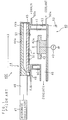
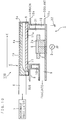
- FIG. 1 shows a conventional microwave plasma processing system 400.
- the system is aimed at independently controlling the generation of a plasma, and the acceleration of ions in the plasma.
- the objectives of the system are to generate a stable bias voltage at the surface of a sample when a high frequency electric field is applied to a sample holder so as to optimize the energy of ions in a plasma, and to perpendicularly irradiate the surface of the sample with ions.
- numeral 40 designates a reactor which is made of a metal such as aluminum, or stainless steel.
- the reactor 40 is airtightly partitioned by a microwave introduction window 45.
- the window consists of a refractory plate made of a material such as quartz glass, or Al2O3 which allows microwaves to be transmitted therethrough, produces a small dielectric loss and has heat resistance.
- a dielectric passage 44 which opposes the microwave introduction window 45 with being separated therefrom by a predetermined distance, and which has a size sufficient for covering the microwave introduction window 45.
- the dielectric passage 44 comprises a dielectric layer 44a which is made of a dielectric material producing a small dielectric loss, such as fluororesin, polystyrene, or polyethylene, and a metal plate 44b which is made of Al or the like and disposed on the upper face of the dielectric layer 44a.
- Microwaves are introduced from a microwave oscillator 47 into the dielectric passage 44 via a waveguide 46.
- the terminal of the dielectric passage 44 is sealed by the metal plate 44b.
- a reaction chamber 41 In the lower portion which is partitioned by the microwave introduction window 45, a reaction chamber 41 is formed.
- a sample stage 42 having a sample holder 42a for holding a sample S which is to be processed is disposed inside the reaction chamber 41.
- a high frequency power source 43 for generating a bias voltage at the surface of the sample S is connected to the sample holder 42a.
- the sample holder 42a is provided with a suction mechanism for sucking the sample S such as an electrostatic chuck, and a cooling mechanism for cooling the sample S which uses a circulating coolant or the like.
- a metal plate 51 which is connected to the ground 52 via the reactor 40 is disposed in closely contact with the lower face of the microwave introduction window 45 which opposes the sample S.
- a large number of slits (or holes) 51a are formed in the metal plate 51 so that microwaves enter the reaction chamber 41.
- the metal plate 51 serves as an anode which is confronted with a cathode (the sample holder 42a) connected to the high frequency power source 43, thereby allowing a distinct bias voltage to be generated to the sample S mounted on the cathode.
- the side wall of the reaction chamber 41 has a double-wall structure so that a cavity serving as a passage 50 for cooling water is formed inside the double-structured side wall.
- a cooling water inlet pipe 50a and a cooling water outlet pipe 50b are communicated with the passage 50.
- a gas supply pipe 48 through which gasses required for generating a plasma are supplied into the reaction chamber 41 is connected to the upper portion of the side wall.
- a gas discharge port 49 which is connected to an evacuating apparatus and through which the reaction chamber 41 is evacuated to attain a vacuum is coupled to the lower portion of the side wall.
- evacuation is conducted through the gas discharge port 49 to set the interior of the reaction chamber 41 to have a predetermined pressure, and reactant gasses are then supplied through the gas supply pipe 48.
- Cooling water is supplied from the cooling water inlet pipe 50a to be circulated in the cavity 50, and then discharged into the cooling water outlet pipe 50b.
- the microwave oscillator 47 oscillates microwaves and the generated microwaves are introduced into the dielectric passage 44 via the waveguide 46 so that an electric field is generated under the dielectric passage 44.
- the generated electric field is transmitted through the microwave introduction window 45 and passes through the slits (or holes) 51a of the grounded metal plate 51 so that a plasma is generated in the reaction chamber 41.
- the high frequency power source 43 applies a high frequency electric field to the sample holder 42a on which the sample S is mounted. Then a stable bias voltage is generated at the surface of the sample S by the action of the grounded metal plate 51. The bias voltage causes the ions to be perpendicularly incident upon the sample S, and controls the energy of the ions incident upon the sample S, whereby the etching conditions are optimized.
- the reactant gasses are introduced into the reaction chamber 41 with passing through the side wall of the reactor 40 (the reaction chamber 41) via the gas supply pipe 48, and are not directly supplied toward the sample S. Therefore, it is difficult to improve the utilization efficiency of reactant gasses, and the gasses flow toward the processed face of the sample S is ununiform. Consequently, it is difficult to improve the uniformities of processing, such as those of the etch rate, and the selection ratio of the SiO2 with respect to Si.
- the microwave transmission holes 51a having a slit-like or circular shape are formed in the metal plate 51.
- the shape of the microwave transmission holes 51a which is suitable for generating a high-density and uniform plasma is not revealed.
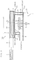
- FIG. 2 is a schematic section view showing a conventional microwave plasma processing system which is proposed by the applicant in Japanese Patent Application Laid-Open No. 6-104098 (1994) with the objective of independently controlling the generation of a plasma and the acceleration of ions in the plasma.
- a metal plate 53 is disposed so as to be in contact with the lower face of a microwave introduction window 45, or to be positioned at the midpoint between the microwave introduction window 45 and a sample holder 42a.
- a plurality of slits 53a which elongate in a direction perpendicular to the microwave traveling direction are formed in the metal plate 53.
- the metal plate 53 is grounded via a reactor 40 (as indicated by 52).
- the sample holder 42a for holding a sample S and a sample stage 54 on which the holder is mounted are disposed at a location opposing the metal plate 53 in a reaction chamber 41.
- the sample stage 54 is coupled with a driving mechanism so as to be vertically moved up and down.
- the other components similar to those of FIG. 1 are designated by the same reference numerals.
- a process of etching the surface of the sample S mounted on the sample holder 42a is performed in the following manner. First, the position of the sample S mounted on the sample holder 42a is adjusted by using the driving mechanism so that the sample is positioned at a predetermined height. Thereafter, evacuation is conducted through the discharge port 49. Reactant gasses are then introduced into the reaction chamber 41 via the gas supply pipe 48 and the interior of the reaction chamber 41 is set to have a desired pressure. Cooling water is supplied from the cooling water inlet pipe 50a to be circulated in the passage 50, and then discharged into the cooling water outlet pipe 50b.
- the microwave oscillator 47 oscillates microwaves and the generated microwaves are introduced into the dielectric passage 44 via the waveguide 46 so that an electric field is generated under the dielectric passage 44.
- the electric field is transmitted through the microwave introduction window 45 and passes through the slits 53a formed in the grounded metal plate 53 so that a plasma is generated in the reaction chamber 41.
- the high frequency power source 43 applies a high frequency electric field to the sample holder 42a so that a stable bias voltage is generated at the surface of the sample S by the action of the grounded metal plate 53.
- etching is performed while the bias voltage which is stably generated causes ions in the plasma to be perpendicularly incident upon the sample S and controls the energy of the ions.
- the grounded metal plate 53 having the slits 53a is disposed so as to be in contact with the microwave introduction window 45 or to be positioned at the midpoint between the microwave introduction window 45 and the sample holder 42a.
- the ground potential with respect to the plasma is made stable so that the plasma potential is stabilized.
- the invention has been conducted in order to solve the above-discussed problems. It is an object of the invention to provide a microwave plasma processing system capable of increasing the efficiency of utilizing reactant gasses and of improving the uniformities of processing, such as those of the etch rate and the selection ratio by uniformalizing the flow of the reactant gasses.
- the microwave plasma processing system is characterized in that a conductor which is disposed with the objective of controlling the anisotropy and the acceleration energy of ions in a plasma has inside a flow path for reactant gasses and also has a plurality of holes through which the gasses are to be blown toward a sample holder.
- the reactant gasses In a microwave plasma processing system, in order to improve the efficiency of utilizing reactant gasses and the uniformities of processing, it is preferable to cause the reactant gasses to perpendicularly or the surface of a sample to be processed. In a process of etching SiO2, particularly, which increase the selection ratio by using the CVD or a deposition film, the uniformities of processing are largely influenced by the flow of the reactant gasses.
- the flow path for reactant gasses is formed in the conductor, and the plurality of holes through which the gasses are blown from the reactant gas flow path toward the sample holder are formed in the face of the conductor opposing the sample holder. Therefore, the reactant gasses are temporarily introduced into the reactant gas flow path and then supplied perpendicularly and uniformly from the plurality of holes to the face of a sample to be processed held by the sample holder.
- This enables the reactant gasses to efficiently reach the face of the sample to be processed in a direct manner. That is, the reactant gasses can reach the face of the sample to be processed without making detour so that the gasses are prevented from being wastefully consumed on the side wall and the like.
- the efficiency of utilizing the reactant gasses can be improved as compared with a conventional microwave plasma processing system.
- the flow of the reactant gasses toward the face of the sample to be processed can be made uniform. Therefore, the uniformities of processing, such as those of the etch rate, and the selection ratio can be improved.
- the microwave plasma processing system according to the invention is characterized in that the ratio of the total area of microwave transmission holes to the outer form area of a grounded conductor is set to be in the range of 0.25 to 0.65.
- the ratio of the total area of the microwave transmission holes to the outer form area of the grounded conductor is set to be equal to or greater than a predetermined value, microwaves can sufficiently be transmitted the sample holder side via the microwave transmission holes so that the plasma is stably generated. Since the ratio of the total area of the microwave transmission holes to the outer form area of the conductor is set to be equal to or smaller than another predetermined value, the ground potential area is ensured and the high bias voltage can be generated at the surface of a sample is stabilized.
- each microwave transmission holes formed in a conductor has a dimension in the microwave traveling direction which is greater than that in a direction perpendicular to the traveling direction.
- microwave transmission holes having a size sufficient for transmission of the electric field based on microwaves must be formed in a grounded conductor disposed on the lower face of a microwave introduction window.
- Microwaves travel in parallel to a dielectric passage (plasma generation plane). In order to generate a uniform plasma, therefore, it is preferable to set the range where a plasma is generated to be always constant as seen a section (FIG. 2) of a reactor perpendicular to the microwave traveling direction.
- each the microwave transmission hole formed in the grounded conductor has a shape which is elongated in the microwave traveling direction and the number of microwave transmission holes arranged in the microwave traveling direction is set to be a value as small as possible.
- the dimension of the microwave transmission holes in the microwave traveling direction is set to be greater than that in a direction perpendicular to the traveling direction, a plasma can be generated in a high density and uniform state.
- FIG. 3 is a section view schematically showing a microwave plasma processing system 100 of Embodiment 1.
- numeral 1 designates a reactor having a hollow rectangular parallelepipedic shape.
- the reactor 1 is made of a metal such as aluminum, or a stainless steel.
- the reactor 1 is airtightly partitioned by a microwave introduction window 5.
- the window 5 consists of a refractory plate made of a material such as quartz glass, or Al2O3 which allows microwaves to be transmitted therethrough, produces a small dielectric loss and has heat resistance.
- a dielectric passage 4 which opposes the microwave introduction window 5 with being separated therefrom by a predetermined distance, and which has a size sufficient for covering the microwave introduction window 5.
- the dielectric passage 4 comprises a dielectric layer 4a which is made of a dielectric material producing a small dielectric loss, such as fluororesin, polystyrene, or polyethylene, and a metal plate 4b which is made of Al or the like and disposed on the upper face of the dielectric layer 4a.
- Microwaves are introduced from a microwave oscillator 7 into the dielectric passage 4 via a waveguide 6.
- the terminal of the dielectric passage 4 is sealed by the metal plate 4b.
- a reaction chamber 21 is formed in the lower portion which is partitioned by the microwave introduction window 5, a reaction chamber 21 is formed.
- a sample stage 2 having a sample holder 2a for holding a sample S which is to be processed is disposed inside the reaction chamber 21.
- a high frequency power source 3 for generating a bias voltage at the surface of the sample S is connected to the sample holder 2a.
- the sample holder 2a is provided with a suction mechanism for sucking the sample S such as an electrostatic chuck or the like, and a cooling mechanism for cooling the sample S which uses a circulating coolant or the like.
- a metal plate 11 which is connected to the ground 22 via the reactor 1 is disposed in closely contact with the lower face of the microwave introduction window 5 which opposes the sample S.
- the metal plate 11 serves as an anode which is confronted with a cathode (the sample holder 2a) connected to the high frequency power source 3, thereby allowing a distinct bias voltage to be generated in the sample S mounted on the catho
- the side wall of the reaction chamber 21 has a double-wall structure so that a cavity serving as a passage 10 for cooling water is formed inside the double-structured side wall. Cooling water is introduced into the passage 10 from a cooling water inlet pipe 10a, and then discharged therefrom into a cooling water outlet pipe 10b.
- a gas supply pipe 8 through which gasses required for generating a plasma are supplied into the reaction chamber 21 is connected to the upper portion of the side wall.
- a gas discharge port 9 which is connected to an evacuating apparatus and through which the reaction chamber 21 is evacuated to attain a vacuum is formed in the lower portion of the side wall.
- the microwave plasma processing system 100 is different in configuration from the conventional microwave plasma processing system 400 shown in FIG. 1 in the following points.
- the metal plate 51 which is the grounded conductor having microwave transmission holes is disposed in closely contact with the lower face of the microwave introduction window 45.
- the metal plate 11 in which a gas buffer room 11a is formed is disposed as the conductor in closely contact with the lower face of the microwave introduction window 5, and the gas supply pipe 8 is communicated with the gas buffer room 11a.
- the configuration of the metal plate 11 will be described with reference to FIG. 4A, 4B.
- FIG. 4A is a perspective view of the metal plate 11 as seen from the side of the microwave introduction window 5, and FIG. 4B is a bottom view showing the face of the metal plate 11 opposing the sample holder 2a.
- slit-like microwave transmission holes 12 are formed in the metal plate 11.
- the microwave transmission holes 12 pierce the metal plate from the face in contact with the microwave introduction window 5 to the face opposing sample holder 2a.
- a gas introduction port 11b through which the gasses are to be introduced from the gas supply pipe 8 into the gas buffer room 11a is formed in the center position of one side face of the metal plate 11.
- a large number of small holes 13 through which the gasses introduced into the gas buffer room 11a are blown from the gas supply pipe 8 toward the face of the sample S to be processed are formed in the face of the metal plate 11 which opposes the sample holder 2a.
- the holes 13 have a predetermined diameter (for example, about 1 mm).
- the metal plate 11 is made of an electrically conductive material such as Al, and connected to the ground 22 via the reactor 1. Therefore, the metal plate 11 serves as the anode electrode with respect to the sample holder 2a (cathode electrode) connected to the high frequency power source 3. Since the microwave transmission holes 12 are formed in the metal plate 11, microwaves are introduced into the reaction chamber 21 via the microwave introduction window 5 and the microwave transmission holes 12.
- the gas introduction port 11b connected to the gas supply pipe 8 is formed in the center position of one side face of the metal plate 11, and the large number of small holes 13 having a predetermined diameter are formed in the face opposing the sample stage 2. Consequently, the gasses supplied through the gas supply pipe 8 are temporarily stored in the gas buffer room 11a, and thereafter blown from the small holes 13 toward the face of the sample S to be processed.
- the metal plate 11 connected to the ground 22 serves as the counter electrode (anode electrode) with respect to the sample holder 2a (cathode electrode) connected to the high frequency power source 3, the plasma potential can be stabilized and a stable bias voltage can be generated at the surface of the sample S in the same manner as the conventional microwave plasma processing system 400.
- This enables the energy of ions in a plasma to be optimized, and ions to be perpendicularly irradiated on the face of the sample S to be processed.
- the microwave plasma processing system 100 additionally, since the gasses are blown from the large number of small holes 13 having the predetermined diameter, the gasses are blown uniformly and perpendicularly with respect to the face of the sample S to be processed so that the flow of the gasses toward the face to be processed can be kept uniform. As compared with the case where the microwave plasma processing system 400 is used, therefore, the use of the microwave plasma processing system 100 can improve the efficiency of utilizing gasses and the uniformities of processing, such as those of the etch rate, and the selection ratio with respect to different materials. The above-discussed contents will be demonstrated with using specific values.
- Processes of etching a silicon oxide film were performed by using the microwave plasma processing system 100 shown in FIG. 3.
- the sample S 8-inch silicon wafers on which an SiO2 film of 1 ⁇ m was formed were used.
- As the reactant gasses CF4, CHF3, and Ar were flown in the amounts of 30 sccm, 30 sccm, and 100 sccm, respectively.
- the gas pressure was 30 mTorr.
- a microwave of a frequency of 2.45 GHz was used, and a plasma was generated at a power of 1 kW.
- a high frequency electric field of a frequency of 400 kHz and a power of 600 W was applied to the sample holder 2a.
- processes of etching an SiO2 film were performed is the same condition as mentioned above by using the microwave plasma processing system 400 shown in FIG. 1. The results were compared with each other. The comparison results are shown in FIGS. 5A and 5B.
- FIG. 5A is a graph showing the results obtained by the microwave plasma processing system 100
- FIG. 5b is a graph showing the results obtained by the microwave plasma processing system 400.
- the curves indicated by ⁇ show the etch rate of the SiO2 film
- the curves indicated by ⁇ show the selection ratio with respect to Si.
- the average etch rate of the SiO2 film was 450 nm/min.
- the uniformity of the etch rate in 8-inch silicon wafers was ⁇ 5 %
- the selection ratio with respect to Si was ⁇ 5 %.
- the average etch rate of the SiO2 film was 400 nm/min.
- the uniformity of the etch rate in 8-inch silicon wafers was ⁇ 5 %
- the selection ratio with respect to Si was ⁇ 15 %. It is considered that the above phenomenon is caused by the following reason.
- the microwave plasma processing system 100 was applied to an etching system.
- the invention is not restricted to this, and can be applied also to other systems such as a thin film forming system.
- the flow path for reactant gasses is disposed inside the conductor, and the plurality of holes through which the gasses are to be blown toward the sample holder are formed in the face of the conductor opposing the sample holder. Therefore, the reactant gasses are temporarily introduced into the flow path, and then blown from the plurality of holes, whereby the reactant gasses can be blown perpendicularly and uniformly to the face of a sample to be processed.
- This enables the reactant gasses to directly reach the face of the sample to be processed in an improved efficiency. Therefore, the reactant gasses can reach the face of the sample to be processed without making detour so that the gasses are prevented from being wastefully consumed on the side wall and the like.
- the efficiency of utilizing the reactant gasses can be improved.
- the flow of the reactant gasses toward the face of the sample to be processed can be made uniform. Therefore, the uniformities of processing, such as those of the etch rate, and the selection ratio can be improved.
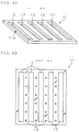
- FIG. 6 is a section view schematically showing a microwave plasma processing system of Embodiment 2.
- a metal plate 15 which is made of aluminum and serves as the conductor is disposed inside the reactor 1 so as to be in parallel with the sample holder 2a.
- a plurality of rectangular microwave transmission holes 15a which elongate in the direction parallel to the microwave traveling direction x as shown in FIG. 7 are formed in the metal plate 15 so that microwaves are transmitted through the microwave introduction window 5 and pass through the microwave transmission holes 15a to be introduced into the reactor 1.
- the grounded metal plate 15 is disposed so as to be in contact with the microwave introduction window 5. The invention is not restricted to this.
- the grounded metal plate 15 may be positioned at the midpoint between the microwave introduction window 5 and the sample holder 2a.
- the material of the metal plate 15 is aluminum.
- the invention is not restricted to this. Any material may be used as far as it is electrically conductive and hardly causes pollution.
- carbon, silicon, or a material having a thin surface oxide film e.g., surface alumite and aluminum may be used.
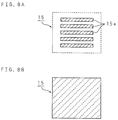
- the hatched portions in FIG. 8A indicate the total area of the microwave transmission holes 15a, and the hatched portion in FIG. 8B indicates the outer form area of the metal plate 15.
- the rectangular microwave transmission holes 15a which elongate in the direction parallel to the microwave traveling direction are formed.
- the invention is not restricted to this.
- a plurality of microwave transmission holes which elongate in direction perpendicular to the microwave traveling direction, or a plurality of circular microwave transmission holes which are not particularly dependent on directions may be formed. Alternatively, these kinds of microwave transmission holes may be formed in combination.
- the grounded metal plate 15 has a rectangular shape.
- the invention is not restricted to this.
- the metal plate may be circular.
- the other components are similar to those of Embodiment 1. These components are designated by the same reference numerals, and their description is omitted.
- results of processes of etching a silicon oxide film (SiO2 film) which were performed by using the microwave plasma processing system of the embodiment will be described.
- etching processes 8-inch silicon wafers on which an SiO2 film of 1 ⁇ m was formed were used as the sample S, and about 30 sccm of CF4, about 30 sccm of CHF3, and about 100 sccm of Ar were supplied as the reactant gasses.
- the gas pressure of the reaction chamber 21 was set to be about 30 mTorr.
- a microwave of a frequency of 2.45 GHz was used, and a plasma was generated at a power of 1 kW.
- a high frequency electric field of a frequency of 400 kHz and a power of 600 W was applied to the sample holder 2a.
- FIG. 9 shows relationships between the ratio of the total area of the microwave transmission holes 15a to the outer form area of the grounded metal plate 15, and the relative etch rate of a silicon oxide film.
- the ratio of the total area of the microwave transmission holes 15a to the outer form area of the grounded metal plate 15 is given by "total area of microwave transmission holes (see FIG. 8A)” / “outer form area of the metal plate (see FIG. 8B)", and the relative etch rate of a silicon oxide film is a relative value which is calculated in the assumption that the etch rate of a silicon oxide film is 1.0 when the ratio is 0.5.
- the results show that, when the ratio is greater than 0.65, the etch rate is lowered to a level which is not desirable in the view point of a practical use.
- this phenomenon is caused by the following reason.
- the ratio is greater than 0.65, the ground potential area is insufficient so that the ground potential with respect to the plasma becomes unstable, and therefore a stable bias voltage is not generated at the surface of the sample S.
- the ratio is smaller than 0.25, flickers of a plasma can be observed visually and it is difficult to maintain a stable plasma discharge state. It is considered that, when the ratio is smaller than 0.25, the transmittance of the microwaves into reaction chamber 21 is reduced and hence the plasma generation cannot be conducted stably.
- the ratio of the total area of microwave transmission holes 15a to the outer form area of the grounded metal plate 15 is preferable to be in the range of 0.25 to 0.65.
- the microwave plasma processing system was used as an etching system.
- the invention is not restricted to this.
- the system of the invention can be used as a thin film forming apparatus.
- the ratio of the total area of microwave transmission holes to the outer form area of the grounded conductor is set to be in the range of 0.25 to 0.65, a plasma can stably be generated and a stable bias voltage can be generated so that a stable plasma processing is performed.
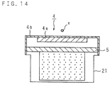
- FIG. 10 is a schematic section view showing a microwave plasma processing system of Embodiment 3.
- a metal plate 17 which serves as the conductor is disposed on the lower face of the microwave introduction window 5.
- a plurality of rectangular microwave transmission holes 17a which elongate in the direction parallel to the microwave traveling direction x as shown in FIG. 11 are formed in the metal plate 17 so that microwaves enter the reaction chamber 21.
- the material of the metal plate 17 is aluminum (Al), and each of the microwave transmission holes 17a have a size of 30 mm ⁇ 300 mm.
- the metal plate 17 serves as a counter electrode with respect to the sample holder 2a, and has a function of generating a stable plasma voltage at the surface of the sample S.
- the other components are similar to those of Embodiment 1. These components are designated by the same reference numerals, and their description is omitted.
- a process of etching the surface of the sample S mounted on the sample holder 2a is performed in the following manner. First, evacuation is conducted through the gas discharge port 9, and reactant gasses are then supplied through the gas supply pipe 8 into the reaction chamber 21 so that the interior of the reaction chamber 21 is set to have a desired degree of vacuum. Cooling water is supplied from the cooling water inlet pipe 10a to be circulated in the passage 10, and then discharged into the cooling water outlet pipe 10b. Then the microwave oscillator 7 oscillates microwaves and the generated microwaves are introduced into the dielectric passage 4 via the waveguide 6 so that an electric field is generated in the lower portion of the dielectric passage 4.
- the generated electric field is transmitted through the microwave introduction window 5 and passes through the microwave transmission holes 17a formed in the grounded metal plate 17, with the result that a plasma is generated in the reaction chamber 21.
- the high frequency power source 3 applies a high frequency electric field to the sample holder 2a so that a stable bias voltage is generated at the surface of the sample S by the action of the grounded metal plate 17.
- the etching process is performed while causing ions in the plasma to be perpendicularly incident upon the surface of the sample S by the stable bias voltage, and controlling the energy of the ions.
- results of processes of etching a silicon oxide film (SiO2 film) which were performed conducted by using the system shown in FIG. 10 will be described.
- a silicon oxide film SiO2 film
- 8-inch silicon wafers on which an SiO2 film of 1 ⁇ m was formed were used as the sample S, and about 30 sccm of CF4, about 30 sccm of CHF3, and about 100 sccm of Ar were supplied as the reactant gasses.
- the gas pressure of the reaction chamber 21 was set to be about 30 mTorr.
- a microwave of a frequency of 2.45 GHz was used, and a plasma was generated at a power of 1.3 kW.
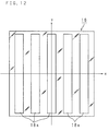
- FIG. 12 shows the metal plate 18 which is obtained by rotating the metal plate 17 shown in FIG. 11 by 90° so that the longitudinal direction of microwave transmission holes 18a is perpendicular to the microwave traveling direction x.
- FIG. 13 shows the metal plate 19 in which 28 microwave transmission holes 19a each having a diameter of 30 mm are formed symmetrically with respect to the center of the plate in such a manner that 20 holes (6 holes per edge) are arranged along the periphery of the plate and 8 holes (3 holes per edge) are formed in the center portion.
- Results show that, in the system having the metal plate 17 shown in FIG. 11, the average etch rate of the SiO2 film was 450 nm/min., and the uniformity of the etch rate in 8-inch silicon wafers was ⁇ 3 %.
- the average etch rate of the SiO2 film was 400 nm/min., and the uniformity of the etch rate in 8-inch silicon wafers was ⁇ 15 %
- the average etch rate of the SiO2 film was 360 nm/min., and the uniformity of the etch rate was ⁇ 5 %.
- the system having the metal plate 17 shown in FIG. 11 exhibits superior results in both the average etch rate and the uniformity of the etch rate. Particularly, there exists a large difference between the effects on the uniformity of the etch rate.
- the system having the metal plate 17 shown in FIG. 11 exhibits superior results in both the average etch rate and the uniformity of the etch rate. Particularly, there exists a large difference between the effects on the average etch rate.
- the system of the embodiment can etch a silicon wafer with a higher speed and in a more stable manner than the systems of the comparison examples.
- the microwave plasma processing system of the embodiment since the dimension of the microwave transmission holes 17a in the microwave traveling direction x in the dielectric passage 4 is greater than that in a direction perpendicular to the direction x, a plasma can be generated in a high density and uniform state and a plasma processing can be performed on the surface of the sample S at a high speed and uniformly.
- the same effects can be expected as far as the conditions that the dimension of the microwave transmission holes 17a in the microwave traveling direction x in the dielectric passage 4 is greater than that in a direction y perpendicular to the traveling direction x are satisfied.
- the number of the microwave transmission holes 17a in the microwave traveling direction x is preferably set to be a value as small as possible.
- the conductor 17 may have microwave transmission holes 17b having elliptic shapes shown in FIG. 15. Further, it may be contemplated that the state same as the above in a pseudo meaning is obtained by forming a large number of small circular microwave transmission holes. As seen from the comparison example of FIG. 13, however, the electric field due to microwaves is largely attenuated when passing through the microwave transmission holes 19a, and hence the process efficiency is lowered.
- the microwave plasma processing system was used as an etching system.
- the invention is not restricted to this.
- the system of the invention can be applied also to other systems such as a thin film forming system and an ashing system.
- the microwave transmission holes having a dimension in the microwave traveling direction which is greater than that in a direction perpendicular to the traveling direction are formed in the grounded conductor in the reactor, a plasma can be generated in a high density and uniform state and a plasma processing can be performed on the surface of a sample at a high speed and uniformly.
Abstract
Description
- The invention relates to a microwave plasma processing system which is used for performing a processing such as etching, ashing, or thin film formation in a production of a semiconductor device.
- In a microwave plasma processing system, a gas discharge is generated in a vacuum vessel under a reduced pressure or a low gas pressure by introducing microwaves into the vessel, thereby generating a plasma, and the surface of a substrate which is a sample is irradiated with the generated plasma so that a processing such as etching, or thin film formation is performed on the substrate. Since such a plasma processing system is essential in the production of a highly integrated semiconductor device and the like, research and development are intensively conducted on the system. Particularly, a microwave plasma processing system in which the generation of a plasma and the acceleration of ions in the generated plasma can independently be controlled is desired in the dry etching technique, and the burying technique for thin film formation.
- FIG. 1 shows a conventional microwave
plasma processing system 400. The system is aimed at independently controlling the generation of a plasma, and the acceleration of ions in the plasma. Specifically, the objectives of the system are to generate a stable bias voltage at the surface of a sample when a high frequency electric field is applied to a sample holder so as to optimize the energy of ions in a plasma, and to perpendicularly irradiate the surface of the sample with ions. In the figure,numeral 40 designates a reactor which is made of a metal such as aluminum, or stainless steel. Thereactor 40 is airtightly partitioned by amicrowave introduction window 45. The window consists of a refractory plate made of a material such as quartz glass, or Al₂O₃ which allows microwaves to be transmitted therethrough, produces a small dielectric loss and has heat resistance. - In the upper portion of the
reactor 40 which is partitioned by themicrowave introduction window 45, disposed is adielectric passage 44 which opposes themicrowave introduction window 45 with being separated therefrom by a predetermined distance, and which has a size sufficient for covering themicrowave introduction window 45. Thedielectric passage 44 comprises a dielectric layer 44a which is made of a dielectric material producing a small dielectric loss, such as fluororesin, polystyrene, or polyethylene, and a metal plate 44b which is made of Al or the like and disposed on the upper face of the dielectric layer 44a. Microwaves are introduced from amicrowave oscillator 47 into thedielectric passage 44 via awaveguide 46. The terminal of thedielectric passage 44 is sealed by the metal plate 44b. - In the lower portion which is partitioned by the
microwave introduction window 45, areaction chamber 41 is formed. Asample stage 42 having a sample holder 42a for holding a sample S which is to be processed is disposed inside thereaction chamber 41. A highfrequency power source 43 for generating a bias voltage at the surface of the sample S is connected to the sample holder 42a. The sample holder 42a is provided with a suction mechanism for sucking the sample S such as an electrostatic chuck, and a cooling mechanism for cooling the sample S which uses a circulating coolant or the like. Ametal plate 51 which is connected to theground 52 via thereactor 40 is disposed in closely contact with the lower face of themicrowave introduction window 45 which opposes the sample S. A large number of slits (or holes) 51a are formed in themetal plate 51 so that microwaves enter thereaction chamber 41. Themetal plate 51 serves as an anode which is confronted with a cathode (the sample holder 42a) connected to the highfrequency power source 43, thereby allowing a distinct bias voltage to be generated to the sample S mounted on the cathode. - The side wall of the
reaction chamber 41 has a double-wall structure so that a cavity serving as apassage 50 for cooling water is formed inside the double-structured side wall. A cooling water inlet pipe 50a and a coolingwater outlet pipe 50b are communicated with thepassage 50. Agas supply pipe 48 through which gasses required for generating a plasma are supplied into thereaction chamber 41 is connected to the upper portion of the side wall. Agas discharge port 49 which is connected to an evacuating apparatus and through which thereaction chamber 41 is evacuated to attain a vacuum is coupled to the lower portion of the side wall. - Hereinafter, the case where a processing, for example, of an etching is to be performed on the surface of the sample S in the thus configured microwave
plasma processing system 400 will be described. - First, evacuation is conducted through the
gas discharge port 49 to set the interior of thereaction chamber 41 to have a predetermined pressure, and reactant gasses are then supplied through thegas supply pipe 48. Cooling water is supplied from the cooling water inlet pipe 50a to be circulated in thecavity 50, and then discharged into the coolingwater outlet pipe 50b. Then themicrowave oscillator 47 oscillates microwaves and the generated microwaves are introduced into thedielectric passage 44 via thewaveguide 46 so that an electric field is generated under thedielectric passage 44. The generated electric field is transmitted through themicrowave introduction window 45 and passes through the slits (or holes) 51a of thegrounded metal plate 51 so that a plasma is generated in thereaction chamber 41. At the same time, in order to control the anisotropy and the acceleration energy of ions in the plasma, the highfrequency power source 43 applies a high frequency electric field to the sample holder 42a on which the sample S is mounted. Then a stable bias voltage is generated at the surface of the sample S by the action of thegrounded metal plate 51. The bias voltage causes the ions to be perpendicularly incident upon the sample S, and controls the energy of the ions incident upon the sample S, whereby the etching conditions are optimized. - In the microwave plasma processing system, the reactant gasses are introduced into the
reaction chamber 41 with passing through the side wall of the reactor 40 (the reaction chamber 41) via thegas supply pipe 48, and are not directly supplied toward the sample S. Therefore, it is difficult to improve the utilization efficiency of reactant gasses, and the gasses flow toward the processed face of the sample S is ununiform. Consequently, it is difficult to improve the uniformities of processing, such as those of the etch rate, and the selection ratio of the SiO₂ with respect to Si. - In order to enable the electric field generated from the
dielectric passage 44 to enter thereaction chamber 41 via themicrowave introduction window 45, the microwave transmission holes 51a having a slit-like or circular shape are formed in themetal plate 51. However, the shape of the microwave transmission holes 51a which is suitable for generating a high-density and uniform plasma is not revealed. - FIG. 2 is a schematic section view showing a conventional microwave plasma processing system which is proposed by the applicant in Japanese Patent Application Laid-Open No. 6-104098 (1994) with the objective of independently controlling the generation of a plasma and the acceleration of ions in the plasma.
- In the system, a
metal plate 53 is disposed so as to be in contact with the lower face of amicrowave introduction window 45, or to be positioned at the midpoint between themicrowave introduction window 45 and a sample holder 42a. A plurality of slits 53a which elongate in a direction perpendicular to the microwave traveling direction are formed in themetal plate 53. Themetal plate 53 is grounded via a reactor 40 (as indicated by 52). The sample holder 42a for holding a sample S and asample stage 54 on which the holder is mounted are disposed at a location opposing themetal plate 53 in areaction chamber 41. Thesample stage 54 is coupled with a driving mechanism so as to be vertically moved up and down. The other components similar to those of FIG. 1 are designated by the same reference numerals. - In the thus configured microwave plasma processing system, for example, a process of etching the surface of the sample S mounted on the sample holder 42a is performed in the following manner. First, the position of the sample S mounted on the sample holder 42a is adjusted by using the driving mechanism so that the sample is positioned at a predetermined height. Thereafter, evacuation is conducted through the
discharge port 49. Reactant gasses are then introduced into thereaction chamber 41 via thegas supply pipe 48 and the interior of thereaction chamber 41 is set to have a desired pressure. Cooling water is supplied from the cooling water inlet pipe 50a to be circulated in thepassage 50, and then discharged into the coolingwater outlet pipe 50b. Then themicrowave oscillator 47 oscillates microwaves and the generated microwaves are introduced into thedielectric passage 44 via thewaveguide 46 so that an electric field is generated under thedielectric passage 44. The electric field is transmitted through themicrowave introduction window 45 and passes through the slits 53a formed in thegrounded metal plate 53 so that a plasma is generated in thereaction chamber 41. Then the highfrequency power source 43 applies a high frequency electric field to the sample holder 42a so that a stable bias voltage is generated at the surface of the sample S by the action of thegrounded metal plate 53. Then etching is performed while the bias voltage which is stably generated causes ions in the plasma to be perpendicularly incident upon the sample S and controls the energy of the ions. - In the microwave plasma processing system, the
grounded metal plate 53 having the slits 53a is disposed so as to be in contact with themicrowave introduction window 45 or to be positioned at the midpoint between themicrowave introduction window 45 and the sample holder 42a. As a result, the ground potential with respect to the plasma is made stable so that the plasma potential is stabilized. When the high frequency electric field is applied to the sample holder 42a, therefore, a stable bias voltage can be generated at the surface of the sample S, the energy of the ions in the plasma can be optimized, and the ions can be perpendicularly irradiated on the surface of the samples. In the case where the ratio of the total area of the slits 53a to the outer form area of themetal plate 53 is small, a stable bias voltage can be generated. In such a case, however, there arises a problem that it is difficult to maintain a stable plasma discharge state based on a sufficient transmission of microwaves. - By contrast, in the case where the ratio of the total area of the slits 53a to the outer form area of the
metal plate 53 is large, a stable plasma discharge can be generated. However, a problem is produced that it is difficult to generate the uniform and high bias voltage based on the distinct ground potential. - The invention has been conducted in order to solve the above-discussed problems. It is an object of the invention to provide a microwave plasma processing system capable of increasing the efficiency of utilizing reactant gasses and of improving the uniformities of processing, such as those of the etch rate and the selection ratio by uniformalizing the flow of the reactant gasses.
- The microwave plasma processing system according to the invention is characterized in that a conductor which is disposed with the objective of controlling the anisotropy and the acceleration energy of ions in a plasma has inside a flow path for reactant gasses and also has a plurality of holes through which the gasses are to be blown toward a sample holder.
- In a microwave plasma processing system, in order to improve the efficiency of utilizing reactant gasses and the uniformities of processing, it is preferable to cause the reactant gasses to perpendicularly or the surface of a sample to be processed. In a process of etching SiO₂, particularly, which increase the selection ratio by using the CVD or a deposition film, the uniformities of processing are largely influenced by the flow of the reactant gasses.
- In the microwave plasma processing system having the above-mentioned configuration, the flow path for reactant gasses is formed in the conductor, and the plurality of holes through which the gasses are blown from the reactant gas flow path toward the sample holder are formed in the face of the conductor opposing the sample holder. Therefore, the reactant gasses are temporarily introduced into the reactant gas flow path and then supplied perpendicularly and uniformly from the plurality of holes to the face of a sample to be processed held by the sample holder. This enables the reactant gasses to efficiently reach the face of the sample to be processed in a direct manner. That is, the reactant gasses can reach the face of the sample to be processed without making detour so that the gasses are prevented from being wastefully consumed on the side wall and the like. Consequently, the efficiency of utilizing the reactant gasses can be improved as compared with a conventional microwave plasma processing system. Moreover, the flow of the reactant gasses toward the face of the sample to be processed can be made uniform. Therefore, the uniformities of processing, such as those of the etch rate, and the selection ratio can be improved.
- It is another object of the invention to provide a microwave plasma processing system in which the plasma potential can be stabilized while stabilizing the plasma discharge, and the bias voltage which is generated at the surface of a sample when a high frequency electric field is applied to the sample via a sample holder can be stabilized.
- The microwave plasma processing system according to the invention is characterized in that the ratio of the total area of microwave transmission holes to the outer form area of a grounded conductor is set to be in the range of 0.25 to 0.65.
- In the microwave plasma processing system having the above-mentioned configuration, since the ratio of the total area of the microwave transmission holes to the outer form area of the grounded conductor is set to be equal to or greater than a predetermined value, microwaves can sufficiently be transmitted the sample holder side via the microwave transmission holes so that the plasma is stably generated. Since the ratio of the total area of the microwave transmission holes to the outer form area of the conductor is set to be equal to or smaller than another predetermined value, the ground potential area is ensured and the high bias voltage can be generated at the surface of a sample is stabilized.
- It is a further object of the invention to provide a microwave plasma processing system in which a distinct bias voltage can be generated at the surface of a sample, and a grounded conductor which can generate a plasma in a high density and uniform state is disposed.
- The microwave plasma processing system according to the invention is characterized in that each microwave transmission holes formed in a conductor has a dimension in the microwave traveling direction which is greater than that in a direction perpendicular to the traveling direction.
- When a processing such as etching, or thin film formation is to be performed on the surface of a sample by irradiation of a plasma generated by an electric field based on microwaves, microwave transmission holes having a size sufficient for transmission of the electric field based on microwaves must be formed in a grounded conductor disposed on the lower face of a microwave introduction window. Microwaves travel in parallel to a dielectric passage (plasma generation plane). In order to generate a uniform plasma, therefore, it is preferable to set the range where a plasma is generated to be always constant as seen a section (FIG. 2) of a reactor perpendicular to the microwave traveling direction. For realization of such a state, it is preferable that each the microwave transmission hole formed in the grounded conductor has a shape which is elongated in the microwave traveling direction and the number of microwave transmission holes arranged in the microwave traveling direction is set to be a value as small as possible.
- In the microwave plasma processing system having the above-mentioned configuration, since the dimension of the microwave transmission holes in the microwave traveling direction is set to be greater than that in a direction perpendicular to the traveling direction, a plasma can be generated in a high density and uniform state.
- The above and further objects and features of the invention will more fully be apparent from the following detailed description with accompanying drawings.
-
- FIG. 1 is a schematic section view showing a conventional microwave plasma processing system;
- FIG. 2 is a schematic section view showing another conventional microwave plasma processing system;
- FIG. 3 is a schematic section view showing a microwave plasma processing system of
Embodiment 1; - FIG. 4A is a perspective view of a metal plate shown in FIG. 3;
- FIG. 4B is a bottom view of the metal plate shown in FIG. 3;
- FIG. 5A is a graph showing the etch rate of an SiO₂ film and the selection ratio of the SiO₂ film with respect to Si in
Embodiment 1; - FIG. 5B is a graph showing the etch rate of an SiO₂ film and the selection ratio of the SiO₂ film with respect to Si in a conventional system;
- FIG. 6 is a schematic section view showing a microwave plasma processing system of
Embodiment 2; - FIG. 7 is a plan view of a metal plate shown in FIG. 6;
- FIG. 8A is a diagram illustrating the total area of microwave transmission holes;
- FIG. 8B is a diagram illustrating the outer form area of a metal plate;
- FIG. 9 is a graph showing a relationship between the ratio of the total area of the microwave transmission holes to the outer form area of the metal plate in
Embodiment 2, and the relative etch rate; - FIG. 10 is a schematic section view showing a microwave plasma processing system of
Embodiment 3; - FIG. 11 is a plan view of a metal plate shown in FIG. 10;
- FIG. 12 is a plan view of a metal plate used in a microwave plasma processing system of a comparison example;
- FIG. 13 is a plan view of a metal plate used in a microwave plasma processing system of another comparison example;
- FIG. 14 is a section view showing a section of the microwave plasma processing system of
Embodiment 3, taken in a direction perpendicular to the microwave traveling direction: and - FIG. 15 is a plan view of another metal plate.
- Hereinafter, the invention will be described in detail with reference to the drawings showing its embodiments.
- FIG. 3 is a section view schematically showing a microwave
plasma processing system 100 ofEmbodiment 1. In the figure, numeral 1 designates a reactor having a hollow rectangular parallelepipedic shape. Thereactor 1 is made of a metal such as aluminum, or a stainless steel. Thereactor 1 is airtightly partitioned by amicrowave introduction window 5. Thewindow 5 consists of a refractory plate made of a material such as quartz glass, or Al₂O₃ which allows microwaves to be transmitted therethrough, produces a small dielectric loss and has heat resistance. - In the upper portion of the
reactor 1 which is partitioned by themicrowave introduction window 5, disposed is adielectric passage 4 which opposes themicrowave introduction window 5 with being separated therefrom by a predetermined distance, and which has a size sufficient for covering themicrowave introduction window 5. Thedielectric passage 4 comprises a dielectric layer 4a which is made of a dielectric material producing a small dielectric loss, such as fluororesin, polystyrene, or polyethylene, and a metal plate 4b which is made of Al or the like and disposed on the upper face of the dielectric layer 4a. Microwaves are introduced from amicrowave oscillator 7 into thedielectric passage 4 via awaveguide 6. The terminal of thedielectric passage 4 is sealed by the metal plate 4b. - In the lower portion which is partitioned by the
microwave introduction window 5, areaction chamber 21 is formed. Asample stage 2 having a sample holder 2a for holding a sample S which is to be processed is disposed inside thereaction chamber 21. A highfrequency power source 3 for generating a bias voltage at the surface of the sample S is connected to the sample holder 2a. The sample holder 2a is provided with a suction mechanism for sucking the sample S such as an electrostatic chuck or the like, and a cooling mechanism for cooling the sample S which uses a circulating coolant or the like. Ametal plate 11 which is connected to theground 22 via thereactor 1 is disposed in closely contact with the lower face of themicrowave introduction window 5 which opposes the sample S. Themetal plate 11 serves as an anode which is confronted with a cathode (the sample holder 2a) connected to the highfrequency power source 3, thereby allowing a distinct bias voltage to be generated in the sample S mounted on the cathode. - The side wall of the
reaction chamber 21 has a double-wall structure so that a cavity serving as apassage 10 for cooling water is formed inside the double-structured side wall. Cooling water is introduced into thepassage 10 from a cooling water inlet pipe 10a, and then discharged therefrom into a cooling water outlet pipe 10b. A gas supply pipe 8 through which gasses required for generating a plasma are supplied into thereaction chamber 21 is connected to the upper portion of the side wall. Agas discharge port 9 which is connected to an evacuating apparatus and through which thereaction chamber 21 is evacuated to attain a vacuum is formed in the lower portion of the side wall. - The microwave
plasma processing system 100 is different in configuration from the conventional microwaveplasma processing system 400 shown in FIG. 1 in the following points. In the microwaveplasma processing system 400, themetal plate 51 which is the grounded conductor having microwave transmission holes is disposed in closely contact with the lower face of themicrowave introduction window 45. By contrast, in the microwaveplasma processing system 100, themetal plate 11 in which a gas buffer room 11a is formed is disposed as the conductor in closely contact with the lower face of themicrowave introduction window 5, and the gas supply pipe 8 is communicated with the gas buffer room 11a. - The configuration of the
metal plate 11 will be described with reference to FIG. 4A, 4B. - FIG. 4A is a perspective view of the
metal plate 11 as seen from the side of themicrowave introduction window 5, and FIG. 4B is a bottom view showing the face of themetal plate 11 opposing the sample holder 2a. As shown in FIG. 4A, slit-like microwave transmission holes 12 are formed in themetal plate 11. The microwave transmission holes 12 pierce the metal plate from the face in contact with themicrowave introduction window 5 to the face opposing sample holder 2a. A gas introduction port 11b through which the gasses are to be introduced from the gas supply pipe 8 into the gas buffer room 11a is formed in the center position of one side face of themetal plate 11. On the other hand, a large number ofsmall holes 13 through which the gasses introduced into the gas buffer room 11a are blown from the gas supply pipe 8 toward the face of the sample S to be processed are formed in the face of themetal plate 11 which opposes the sample holder 2a. Theholes 13 have a predetermined diameter (for example, about 1 mm). - The
metal plate 11 is made of an electrically conductive material such as Al, and connected to theground 22 via thereactor 1. Therefore, themetal plate 11 serves as the anode electrode with respect to the sample holder 2a (cathode electrode) connected to the highfrequency power source 3. Since the microwave transmission holes 12 are formed in themetal plate 11, microwaves are introduced into thereaction chamber 21 via themicrowave introduction window 5 and the microwave transmission holes 12. The gas introduction port 11b connected to the gas supply pipe 8 is formed in the center position of one side face of themetal plate 11, and the large number ofsmall holes 13 having a predetermined diameter are formed in the face opposing thesample stage 2. Consequently, the gasses supplied through the gas supply pipe 8 are temporarily stored in the gas buffer room 11a, and thereafter blown from thesmall holes 13 toward the face of the sample S to be processed. - As seen from the above description, in the microwave
plasma processing system 100 of the embodiment, since themetal plate 11 connected to theground 22 serves as the counter electrode (anode electrode) with respect to the sample holder 2a (cathode electrode) connected to the highfrequency power source 3, the plasma potential can be stabilized and a stable bias voltage can be generated at the surface of the sample S in the same manner as the conventional microwaveplasma processing system 400. This enables the energy of ions in a plasma to be optimized, and ions to be perpendicularly irradiated on the face of the sample S to be processed. In the microwaveplasma processing system 100, additionally, since the gasses are blown from the large number ofsmall holes 13 having the predetermined diameter, the gasses are blown uniformly and perpendicularly with respect to the face of the sample S to be processed so that the flow of the gasses toward the face to be processed can be kept uniform. As compared with the case where the microwaveplasma processing system 400 is used, therefore, the use of the microwaveplasma processing system 100 can improve the efficiency of utilizing gasses and the uniformities of processing, such as those of the etch rate, and the selection ratio with respect to different materials. The above-discussed contents will be demonstrated with using specific values. - Processes of etching a silicon oxide film (SiO₂ film) were performed by using the microwave
plasma processing system 100 shown in FIG. 3. As the sample S, 8-inch silicon wafers on which an SiO₂ film of 1 µ m was formed were used. As the reactant gasses, CF₄, CHF₃, and Ar were flown in the amounts of 30 sccm, 30 sccm, and 100 sccm, respectively. The gas pressure was 30 mTorr. A microwave of a frequency of 2.45 GHz was used, and a plasma was generated at a power of 1 kW. A high frequency electric field of a frequency of 400 kHz and a power of 600 W was applied to the sample holder 2a. As a comparison example, processes of etching an SiO₂ film were performed is the same condition as mentioned above by using the microwaveplasma processing system 400 shown in FIG. 1. The results were compared with each other. The comparison results are shown in FIGS. 5A and 5B. - FIG. 5A is a graph showing the results obtained by the microwave
plasma processing system 100, and FIG. 5b is a graph showing the results obtained by the microwaveplasma processing system 400. In FIGS. 5A and 5B, the curves indicated by ○ show the etch rate of the SiO₂ film, and the curves indicated by △ show the selection ratio with respect to Si. The abscissae show the distance from the center (= 0 mm) of the silicon wafer. - In the case where the microwave
plasma processing system 100 was used, the average etch rate of the SiO₂ film was 450 nm/min., the uniformity of the etch rate in 8-inch silicon wafers was ± 5 %, and the selection ratio with respect to Si was ± 5 %. By contrast, in the case where the microwaveplasma processing system 400 was used, the average etch rate of the SiO₂ film was 400 nm/min., and the uniformity of the etch rate in 8-inch silicon wafers was ± 5 %, but the selection ratio with respect to Si was ± 15 %. It is considered that the above phenomenon is caused by the following reason. In the etching of the SiO₂ film, energies are given to ions by the bias voltage, and the etching process is caused to proceed by the energies. When the plasma and the bias voltage are uniformly distributed, therefore, a uniform etching distribution is obtained. In contrast, it is considered that the etching of Si is caused to proceed by a chemical reaction due to neutral radicals, and hence depends on the gas flow. - In the above, the embodiment in which the microwave
plasma processing system 100 was applied to an etching system has been described. The invention is not restricted to this, and can be applied also to other systems such as a thin film forming system. - As described above in detail, according to the embodiment, the flow path for reactant gasses is disposed inside the conductor, and the plurality of holes through which the gasses are to be blown toward the sample holder are formed in the face of the conductor opposing the sample holder. Therefore, the reactant gasses are temporarily introduced into the flow path, and then blown from the plurality of holes, whereby the reactant gasses can be blown perpendicularly and uniformly to the face of a sample to be processed. This enables the reactant gasses to directly reach the face of the sample to be processed in an improved efficiency. Therefore, the reactant gasses can reach the face of the sample to be processed without making detour so that the gasses are prevented from being wastefully consumed on the side wall and the like. Consequently, the efficiency of utilizing the reactant gasses can be improved. Moreover, the flow of the reactant gasses toward the face of the sample to be processed can be made uniform. Therefore, the uniformities of processing, such as those of the etch rate, and the selection ratio can be improved.
- FIG. 6 is a section view schematically showing a microwave plasma processing system of
Embodiment 2. In the embodiment, ametal plate 15 which is made of aluminum and serves as the conductor is disposed inside thereactor 1 so as to be in parallel with the sample holder 2a. A plurality of rectangular microwave transmission holes 15a which elongate in the direction parallel to the microwave traveling direction x as shown in FIG. 7 are formed in themetal plate 15 so that microwaves are transmitted through themicrowave introduction window 5 and pass through the microwave transmission holes 15a to be introduced into thereactor 1. In the embodiment, the groundedmetal plate 15 is disposed so as to be in contact with themicrowave introduction window 5. The invention is not restricted to this. The groundedmetal plate 15 may be positioned at the midpoint between themicrowave introduction window 5 and the sample holder 2a. In the embodiment, the material of themetal plate 15 is aluminum. The invention is not restricted to this. Any material may be used as far as it is electrically conductive and hardly causes pollution. For example, carbon, silicon, or a material having a thin surface oxide film (e.g., surface alumite and aluminum) may be used. - The hatched portions in FIG. 8A indicate the total area of the microwave transmission holes 15a, and the hatched portion in FIG. 8B indicates the outer form area of the
metal plate 15. In the embodiment, the rectangular microwave transmission holes 15a which elongate in the direction parallel to the microwave traveling direction are formed. The invention is not restricted to this. A plurality of microwave transmission holes which elongate in direction perpendicular to the microwave traveling direction, or a plurality of circular microwave transmission holes which are not particularly dependent on directions may be formed. Alternatively, these kinds of microwave transmission holes may be formed in combination. In the embodiment, the groundedmetal plate 15 has a rectangular shape. The invention is not restricted to this. The metal plate may be circular. The other components are similar to those ofEmbodiment 1. These components are designated by the same reference numerals, and their description is omitted. - Hereinafter, results of processes of etching a silicon oxide film (SiO₂ film) which were performed by using the microwave plasma processing system of the embodiment will be described. In the etching processes, 8-inch silicon wafers on which an SiO₂ film of 1 µ m was formed were used as the sample S, and about 30 sccm of CF₄, about 30 sccm of CHF₃, and about 100 sccm of Ar were supplied as the reactant gasses. The gas pressure of the
reaction chamber 21 was set to be about 30 mTorr. A microwave of a frequency of 2.45 GHz was used, and a plasma was generated at a power of 1 kW. A high frequency electric field of a frequency of 400 kHz and a power of 600 W was applied to the sample holder 2a. - FIG. 9 shows relationships between the ratio of the total area of the microwave transmission holes 15a to the outer form area of the grounded
metal plate 15, and the relative etch rate of a silicon oxide film. The ratio of the total area of the microwave transmission holes 15a to the outer form area of the groundedmetal plate 15 is given by "total area of microwave transmission holes (see FIG. 8A)" / "outer form area of the metal plate (see FIG. 8B)", and the relative etch rate of a silicon oxide film is a relative value which is calculated in the assumption that the etch rate of a silicon oxide film is 1.0 when the ratio is 0.5. The results show that, when the ratio is greater than 0.65, the etch rate is lowered to a level which is not desirable in the view point of a practical use. It is considered that this phenomenon is caused by the following reason. When the ratio is greater than 0.65, the ground potential area is insufficient so that the ground potential with respect to the plasma becomes unstable, and therefore a stable bias voltage is not generated at the surface of the sample S. In contrast, when the ratio is smaller than 0.25, flickers of a plasma can be observed visually and it is difficult to maintain a stable plasma discharge state. It is considered that, when the ratio is smaller than 0.25, the transmittance of the microwaves intoreaction chamber 21 is reduced and hence the plasma generation cannot be conducted stably. - As seen from the results, it is preferable to set the ratio of the total area of microwave transmission holes 15a to the outer form area of the grounded
metal plate 15 to be in the range of 0.25 to 0.65. - In the above, the embodiment in which the microwave plasma processing system was used as an etching system has been described. The invention is not restricted to this. For example, the system of the invention can be used as a thin film forming apparatus.
- As described above in detail, according to the embodiment, since the ratio of the total area of microwave transmission holes to the outer form area of the grounded conductor is set to be in the range of 0.25 to 0.65, a plasma can stably be generated and a stable bias voltage can be generated so that a stable plasma processing is performed.
- FIG. 10 is a schematic section view showing a microwave plasma processing system of
Embodiment 3. Ametal plate 17 which serves as the conductor is disposed on the lower face of themicrowave introduction window 5. A plurality of rectangular microwave transmission holes 17a which elongate in the direction parallel to the microwave traveling direction x as shown in FIG. 11 are formed in themetal plate 17 so that microwaves enter thereaction chamber 21. In the embodiment, the material of themetal plate 17 is aluminum (Al), and each of the microwave transmission holes 17a have a size of 30 mm × 300 mm. Themetal plate 17 serves as a counter electrode with respect to the sample holder 2a, and has a function of generating a stable plasma voltage at the surface of the sample S. The other components are similar to those ofEmbodiment 1. These components are designated by the same reference numerals, and their description is omitted. - In the thus configured microwave plasma processing system, for example, a process of etching the surface of the sample S mounted on the sample holder 2a is performed in the following manner. First, evacuation is conducted through the
gas discharge port 9, and reactant gasses are then supplied through the gas supply pipe 8 into thereaction chamber 21 so that the interior of thereaction chamber 21 is set to have a desired degree of vacuum. Cooling water is supplied from the cooling water inlet pipe 10a to be circulated in thepassage 10, and then discharged into the cooling water outlet pipe 10b. Then themicrowave oscillator 7 oscillates microwaves and the generated microwaves are introduced into thedielectric passage 4 via thewaveguide 6 so that an electric field is generated in the lower portion of thedielectric passage 4. The generated electric field is transmitted through themicrowave introduction window 5 and passes through the microwave transmission holes 17a formed in the groundedmetal plate 17, with the result that a plasma is generated in thereaction chamber 21. Then the highfrequency power source 3 applies a high frequency electric field to the sample holder 2a so that a stable bias voltage is generated at the surface of the sample S by the action of the groundedmetal plate 17. Then the etching process is performed while causing ions in the plasma to be perpendicularly incident upon the surface of the sample S by the stable bias voltage, and controlling the energy of the ions. - Hereinafter, results of processes of etching a silicon oxide film (SiO₂ film) which were performed conducted by using the system shown in FIG. 10 will be described. In the etching processes, 8-inch silicon wafers on which an SiO₂ film of 1 µ m was formed were used as the sample S, and about 30 sccm of CF₄, about 30 sccm of CHF₃, and about 100 sccm of Ar were supplied as the reactant gasses. The gas pressure of the
reaction chamber 21 was set to be about 30 mTorr. A microwave of a frequency of 2.45 GHz was used, and a plasma was generated at a power of 1.3 kW. A high frequency electric field of a frequency of 400 kHz and a power of 600 W was applied to the sample holder 2a. As comparison examples, experiments using groundedmetal plates metal plate 18 which is obtained by rotating themetal plate 17 shown in FIG. 11 by 90° so that the longitudinal direction of microwave transmission holes 18a is perpendicular to the microwave traveling direction x. FIG. 13 shows themetal plate 19 in which 28 microwave transmission holes 19a each having a diameter of 30 mm are formed symmetrically with respect to the center of the plate in such a manner that 20 holes (6 holes per edge) are arranged along the periphery of the plate and 8 holes (3 holes per edge) are formed in the center portion. - Results show that, in the system having the
metal plate 17 shown in FIG. 11, the average etch rate of the SiO₂ film was 450 nm/min., and the uniformity of the etch rate in 8-inch silicon wafers was ± 3 %. By contrast, in the system having themetal plate 18 shown in FIG. 12, the average etch rate of the SiO₂ film was 400 nm/min., and the uniformity of the etch rate in 8-inch silicon wafers was ± 15 %, and, in the system having themetal plate 19 shown in FIG. 13, the average etch rate of the SiO₂ film was 360 nm/min., and the uniformity of the etch rate was ± 5 %. - When compared the results of the systems shown in FIGS. 11 and 12 with each other, the system having the
metal plate 17 shown in FIG. 11 exhibits superior results in both the average etch rate and the uniformity of the etch rate. Particularly, there exists a large difference between the effects on the uniformity of the etch rate. When compared the results of the systems having the metal plates shown in FIGS. 11 and 13 with each other, the system having themetal plate 17 shown in FIG. 11 exhibits superior results in both the average etch rate and the uniformity of the etch rate. Particularly, there exists a large difference between the effects on the average etch rate. - As seen from the above-mentioned results, the system of the embodiment can etch a silicon wafer with a higher speed and in a more stable manner than the systems of the comparison examples. In this way, in the microwave plasma processing system of the embodiment, since the dimension of the microwave transmission holes 17a in the microwave traveling direction x in the
dielectric passage 4 is greater than that in a direction perpendicular to the direction x, a plasma can be generated in a high density and uniform state and a plasma processing can be performed on the surface of the sample S at a high speed and uniformly. - Even when a plurality of rectangular slits are formed as the microwave transmission holes in the direction x, the same effects can be expected as far as the conditions that the dimension of the microwave transmission holes 17a in the microwave traveling direction x in the
dielectric passage 4 is greater than that in a direction y perpendicular to the traveling direction x are satisfied. In the view point of the uniformity of plasma generation, however, the number of the microwave transmission holes 17a in the microwave traveling direction x is preferably set to be a value as small as possible. Moreover, theconductor 17 may have microwave transmission holes 17b having elliptic shapes shown in FIG. 15. Further, it may be contemplated that the state same as the above in a pseudo meaning is obtained by forming a large number of small circular microwave transmission holes. As seen from the comparison example of FIG. 13, however, the electric field due to microwaves is largely attenuated when passing through the microwave transmission holes 19a, and hence the process efficiency is lowered. - In the above, the embodiment in which the microwave plasma processing system was used as an etching system has been described. The invention is not restricted to this. For example, the system of the invention can be applied also to other systems such as a thin film forming system and an ashing system.
- As described above in detail, according to the embodiment, since the microwave transmission holes having a dimension in the microwave traveling direction which is greater than that in a direction perpendicular to the traveling direction are formed in the grounded conductor in the reactor, a plasma can be generated in a high density and uniform state and a plasma processing can be performed on the surface of a sample at a high speed and uniformly.
- As this invention may be embodied in several forms without departing from the spirit of essential characteristics thereof, the present embodiment is therefore illustrative and not restrictive, since the scope of the invention is defined by the appended claims rather than by the description preceding them, and all changes that fall within metes and bounds of the claims, or equivalence of such metes and bounds thereof are therefore intended to be embraced by the claims.
Claims (8)
- A microwave plasma processing system in which a microwave oscillated by a microwave oscillator (7) is introduced to a dielectric passage (4) in a reactor (1) via a waveguide (6), the microwave passing through a microwave introduction window (5) and a conductor is introduced to a reaction chamber (21) to which a reactant gas is supplied, and a sample (S) held on a sample holder (2a) to which an electric field is supplied, characterized in that said conductor (11) is disposed between said microwave introduction window (5) and said sample holder (2a), and has microwave transmission holes (12), a flow path (11a) communicated with gas supplying means, and holes (13) through which the reactant gas is to be blown toward a sample (S).
- A microwave plasma processing system according to claim 1, wherein said conductor (11) is disposed in contact with said microwave introduction window (5).
- A microwave plasma processing system in which a microwave oscillated by a microwave oscillator (7) is introduced to a dielectric passage (4) in a reactor (1) via a waveguide (6), the microwave passing through a microwave introduction window (5) and a conductor is introduced to a reaction chamber (21) to which a reactant gas is supplied, and a sample (S) held on a sample holder (2a) to which an electric field is supplied, characterized in that said conductor (15) has microwave transmission holes, and a ratio of a total area of said microwave transmission holes (15a) to an area of said conductor (15) is in the range of 0.25 to 0.65.
- A microwave plasma processing system according to claim 3, wherein said conductor (15) is disposed in contact with said microwave introduction window (5).
- A microwave plasma processing system in which a microwave oscillated by a microwave oscillator (7) is introduced to a dielectric passage (4) in a reactor (1) via a waveguide (6), the microwave passing through a microwave introduction window (5) and a conductor is introduced to a reaction chamber (21) to which a reactant gas is supplied, and a sample (S) held on a sample holder (2a) to which an electric field is supplied, characterized in that said conductor (17) has microwave transmission holes, and a dimension of each of said microwave transmission holes (17a) in a microwave traveling direction (x) on said dielectric passage (4) is greater than that in a direction perpendicular to said microwave traveling direction.
- A microwave plasma processing system according to claim 5, wherein each of said microwave transmission holes (17a) has a rectangular shape.
- A microwave plasma processing system according to claim 5, wherein each of said microwave transmission holes (17b) has an elliptic shape.
- A microwave plasma processing system according to claim 5, wherein said conductor (17) is disposed in contact with said microwave introduction window (5).
Applications Claiming Priority (9)
| Application Number | Priority Date | Filing Date | Title |
|---|---|---|---|
| JP132031/94 | 1994-06-14 | ||
| JP6132032A JPH083770A (en) | 1994-06-14 | 1994-06-14 | Microwave plasma treatment device |
| JP13203194A JP3164188B2 (en) | 1994-06-14 | 1994-06-14 | Plasma processing equipment |
| JP132033/94 | 1994-06-14 | ||
| JP132032/94 | 1994-06-14 | ||
| JP13203294 | 1994-06-14 | ||
| JP13203394 | 1994-06-14 | ||
| JP13203194 | 1994-06-14 | ||
| JP6132033A JPH07335393A (en) | 1994-06-14 | 1994-06-14 | Microwave plasma treatment device |
Publications (3)
| Publication Number | Publication Date |
|---|---|
| EP0688038A2 true EP0688038A2 (en) | 1995-12-20 |
| EP0688038A3 EP0688038A3 (en) | 1996-04-17 |
| EP0688038B1 EP0688038B1 (en) | 2001-12-19 |
Family
ID=27316416
Family Applications (1)
| Application Number | Title | Priority Date | Filing Date |
|---|---|---|---|
| EP95109090A Expired - Lifetime EP0688038B1 (en) | 1994-06-14 | 1995-06-13 | Microwave plasma processing system |
Country Status (4)
| Country | Link |
|---|---|
| US (1) | US5545258A (en) |
| EP (1) | EP0688038B1 (en) |
| KR (1) | KR0153842B1 (en) |
| DE (1) | DE69524671T2 (en) |
Cited By (6)
| Publication number | Priority date | Publication date | Assignee | Title |
|---|---|---|---|---|
| EP0749149A2 (en) * | 1995-06-15 | 1996-12-18 | Sumitomo Metal Industries, Ltd. | Plasma processing apparatus |
| EP0749148A2 (en) * | 1995-06-15 | 1996-12-18 | Sumitomo Metal Industries, Ltd. | Plasma processing apparatus |
| EP1006761A1 (en) * | 1998-06-19 | 2000-06-07 | Sumitomo Metal Industries, Ltd. | Plasma processor |
| EP1531487A3 (en) * | 2003-11-17 | 2006-02-01 | Ulvac Inc. | Microwave-excited plasma processing apparatus |
| CN109616413A (en) * | 2015-11-04 | 2019-04-12 | 朗姆研究公司 | For carrying out the method and system of advanced ionic control to etch process |
| CN113631016A (en) * | 2021-08-06 | 2021-11-09 | 中国电子科技集团公司第三十八研究所 | Integrated three-dimensional liquid cooling pipe network flow distribution device |
Families Citing this family (31)
| Publication number | Priority date | Publication date | Assignee | Title |
|---|---|---|---|---|
| JP3257328B2 (en) * | 1995-03-16 | 2002-02-18 | 株式会社日立製作所 | Plasma processing apparatus and plasma processing method |
| US5571577A (en) * | 1995-04-07 | 1996-11-05 | Board Of Trustees Operating Michigan State University | Method and apparatus for plasma treatment of a surface |
| US5698036A (en) * | 1995-05-26 | 1997-12-16 | Tokyo Electron Limited | Plasma processing apparatus |
| JP3585578B2 (en) * | 1995-05-30 | 2004-11-04 | アネルバ株式会社 | Plasma processing equipment |
| KR100293033B1 (en) * | 1996-03-28 | 2001-06-15 | 고지마 마타오 | Plasma treatment apparatus and plasma treatment method |
| US6092486A (en) * | 1996-05-27 | 2000-07-25 | Sumimoto Metal Indsutries, Ltd. | Plasma processing apparatus and plasma processing method |
| KR980001977A (en) * | 1996-06-29 | 1998-03-30 | 유충식 | Fermentation composition for biological treatment of food waste and composting method |
| US6432203B1 (en) * | 1997-03-17 | 2002-08-13 | Applied Komatsu Technology, Inc. | Heated and cooled vacuum chamber shield |
| US6209482B1 (en) * | 1997-10-01 | 2001-04-03 | Energy Conversion Devices, Inc. | Large area microwave plasma apparatus with adaptable applicator |
| JP3430053B2 (en) * | 1999-02-01 | 2003-07-28 | 東京エレクトロン株式会社 | Plasma processing equipment |
| KR100319894B1 (en) * | 1999-07-13 | 2002-01-10 | 윤종용 | Etching method of material fim formed on semiconductor wafer using surface wave coupled plasma etching apparatus |
| JP4222707B2 (en) * | 2000-03-24 | 2009-02-12 | 東京エレクトロン株式会社 | Plasma processing apparatus and method, gas supply ring and dielectric |
| US6544895B1 (en) * | 2000-08-17 | 2003-04-08 | Micron Technology, Inc. | Methods for use of pulsed voltage in a plasma reactor |
| US6485572B1 (en) * | 2000-08-28 | 2002-11-26 | Micron Technology, Inc. | Use of pulsed grounding source in a plasma reactor |
| JP2002134417A (en) * | 2000-10-23 | 2002-05-10 | Tokyo Electron Ltd | Plasma processing system |
| JP3650025B2 (en) * | 2000-12-04 | 2005-05-18 | シャープ株式会社 | Plasma process equipment |
| KR100456451B1 (en) * | 2002-01-15 | 2004-11-09 | 이헌구 | Manufacturing method of Bio-fertilizer using useless sugars |
| US6845734B2 (en) * | 2002-04-11 | 2005-01-25 | Micron Technology, Inc. | Deposition apparatuses configured for utilizing phased microwave radiation |
| KR101096950B1 (en) * | 2004-03-19 | 2011-12-20 | 샤프 가부시키가이샤 | Plasma Treatment Apparatus and Plasma Treatment Method |
| US7842135B2 (en) * | 2006-01-09 | 2010-11-30 | Aixtron Ag | Equipment innovations for nano-technology aquipment, especially for plasma growth chambers of carbon nanotube and nanowire |
| JP2010016225A (en) * | 2008-07-04 | 2010-01-21 | Tokyo Electron Ltd | Thermal control mechanism and semiconductor manufacturing device using the same |
| JP5375732B2 (en) * | 2010-04-26 | 2013-12-25 | 株式会社島津製作所 | Method for forming barrier film and CVD apparatus used for forming barrier film |
| JP5466670B2 (en) * | 2010-10-28 | 2014-04-09 | 株式会社日立国際電気 | Substrate processing apparatus and semiconductor device manufacturing method |
| JP5256328B2 (en) * | 2010-10-28 | 2013-08-07 | 株式会社日立国際電気 | Substrate processing apparatus and semiconductor device manufacturing method |
| US9543123B2 (en) * | 2011-03-31 | 2017-01-10 | Tokyo Electronics Limited | Plasma processing apparatus and plasma generation antenna |
| JP2014026773A (en) * | 2012-07-25 | 2014-02-06 | Tokyo Electron Ltd | Plasma processing apparatus |
| US20140042152A1 (en) * | 2012-08-08 | 2014-02-13 | Taiwan Semiconductor Manufacturing Company, Ltd. | Variable frequency microwave device and method for rectifying wafer warpage |
| JP6144902B2 (en) | 2012-12-10 | 2017-06-07 | 東京エレクトロン株式会社 | Microwave radiation antenna, microwave plasma source, and plasma processing apparatus |
| JP5432395B1 (en) * | 2013-02-28 | 2014-03-05 | 三井造船株式会社 | Film forming apparatus and film forming method |
| US20140363903A1 (en) * | 2013-06-10 | 2014-12-11 | Tokyo Ohta Kogyo Co., Ltd. | Substrate treating apparatus and method of treating substrate |
| JP6356415B2 (en) | 2013-12-16 | 2018-07-11 | 東京エレクトロン株式会社 | Microwave plasma source and plasma processing apparatus |
Citations (1)
| Publication number | Priority date | Publication date | Assignee | Title |
|---|---|---|---|---|
| JPH06104098A (en) | 1992-09-22 | 1994-04-15 | Sumitomo Metal Ind Ltd | Microwave plasma treatment device |
Family Cites Families (8)
| Publication number | Priority date | Publication date | Assignee | Title |
|---|---|---|---|---|
| JPS61131454A (en) * | 1984-11-30 | 1986-06-19 | Fujitsu Ltd | Microwave plasma process and device therefor |
| US5364519A (en) * | 1984-11-30 | 1994-11-15 | Fujitsu Limited | Microwave plasma processing process and apparatus |
| EP0264913B1 (en) * | 1986-10-20 | 1994-06-22 | Hitachi, Ltd. | Plasma processing apparatus |
| DE3830249A1 (en) * | 1988-09-06 | 1990-03-15 | Schott Glaswerke | PLASMA PROCESS FOR COATING LEVEL SUBSTRATES |
| US5134965A (en) * | 1989-06-16 | 1992-08-04 | Hitachi, Ltd. | Processing apparatus and method for plasma processing |
| JPH03191074A (en) * | 1989-12-20 | 1991-08-21 | Canon Inc | Microwave plasma treating device |
| KR0156011B1 (en) * | 1991-08-12 | 1998-12-01 | 이노우에 아키라 | Plasma treating apparatus and method thereof |
| JP2570090B2 (en) * | 1992-10-08 | 1997-01-08 | 日本電気株式会社 | Dry etching equipment |
-
1995
- 1995-06-13 US US08/490,088 patent/US5545258A/en not_active Expired - Lifetime
- 1995-06-13 DE DE69524671T patent/DE69524671T2/en not_active Expired - Fee Related
- 1995-06-13 KR KR1019950015464A patent/KR0153842B1/en not_active IP Right Cessation
- 1995-06-13 EP EP95109090A patent/EP0688038B1/en not_active Expired - Lifetime
Patent Citations (1)
| Publication number | Priority date | Publication date | Assignee | Title |
|---|---|---|---|---|
| JPH06104098A (en) | 1992-09-22 | 1994-04-15 | Sumitomo Metal Ind Ltd | Microwave plasma treatment device |
Cited By (14)
| Publication number | Priority date | Publication date | Assignee | Title |
|---|---|---|---|---|
| EP0749148A2 (en) * | 1995-06-15 | 1996-12-18 | Sumitomo Metal Industries, Ltd. | Plasma processing apparatus |
| EP0749148A3 (en) * | 1995-06-15 | 1999-01-20 | Sumitomo Metal Industries, Ltd. | Plasma processing apparatus |
| EP0749149A3 (en) * | 1995-06-15 | 1999-01-20 | Sumitomo Metal Industries, Ltd. | Plasma processing apparatus |
| US5911852A (en) * | 1995-06-15 | 1999-06-15 | Sumitomo Metal Industries Limited | Plasma processing apparatus |
| EP0749149A2 (en) * | 1995-06-15 | 1996-12-18 | Sumitomo Metal Industries, Ltd. | Plasma processing apparatus |
| EP1006761A4 (en) * | 1998-06-19 | 2007-05-16 | Tokyo Electron Ltd | Plasma processor |
| EP1006761A1 (en) * | 1998-06-19 | 2000-06-07 | Sumitomo Metal Industries, Ltd. | Plasma processor |
| EP1531487A3 (en) * | 2003-11-17 | 2006-02-01 | Ulvac Inc. | Microwave-excited plasma processing apparatus |
| US7392760B2 (en) | 2003-11-17 | 2008-07-01 | Ulvac, Inc. | Microwave-excited plasma processing apparatus |
| CN100405533C (en) * | 2003-11-17 | 2008-07-23 | 爱发科股份有限公司 | Microwave-excited plasma processing apparatus |
| CN109616413A (en) * | 2015-11-04 | 2019-04-12 | 朗姆研究公司 | For carrying out the method and system of advanced ionic control to etch process |
| CN109616413B (en) * | 2015-11-04 | 2023-09-29 | 朗姆研究公司 | Method and system for advanced ion control of etching process |
| CN113631016A (en) * | 2021-08-06 | 2021-11-09 | 中国电子科技集团公司第三十八研究所 | Integrated three-dimensional liquid cooling pipe network flow distribution device |
| CN113631016B (en) * | 2021-08-06 | 2023-05-16 | 中国电子科技集团公司第三十八研究所 | Integrated three-dimensional liquid cooling pipe network flow distribution device |
Also Published As
| Publication number | Publication date |
|---|---|
| US5545258A (en) | 1996-08-13 |
| DE69524671D1 (en) | 2002-01-31 |
| EP0688038B1 (en) | 2001-12-19 |
| KR0153842B1 (en) | 1998-12-01 |
| DE69524671T2 (en) | 2002-08-14 |
| KR960002627A (en) | 1996-01-26 |
| EP0688038A3 (en) | 1996-04-17 |
Similar Documents
| Publication | Publication Date | Title |
|---|---|---|
| US5545258A (en) | Microwave plasma processing system | |
| US5951887A (en) | Plasma processing apparatus and plasma processing method | |
| US5753066A (en) | Plasma source for etching | |
| US6348158B1 (en) | Plasma processing with energy supplied | |
| EP0688037B1 (en) | Microwave plasma processing system | |
| US5242539A (en) | Plasma treatment method and apparatus | |
| US5851600A (en) | Plasma process method and apparatus | |
| US5911852A (en) | Plasma processing apparatus | |
| JP2748886B2 (en) | Plasma processing equipment | |
| KR101341371B1 (en) | Plasma processing device and plasma processing method | |
| JP2001520452A (en) | Apparatus and method for adjusting plasma density distribution | |
| US5804923A (en) | Plasma processing apparatus having a protected microwave transmission window | |
| JP3042208B2 (en) | Microwave plasma processing equipment | |
| JP2021034515A (en) | Cleaning method and microwave plasma processor | |
| JP2662219B2 (en) | Plasma processing equipment | |
| JP2569019B2 (en) | Etching method and apparatus | |
| JP3164188B2 (en) | Plasma processing equipment | |
| US6027662A (en) | Materials processing by separately generated process medium constituents | |
| EP0512677A2 (en) | Plasma treatment method and apparatus | |
| JP3147769B2 (en) | Plasma processing apparatus and processing method | |
| JP2800766B2 (en) | Plasma processing method and apparatus | |
| JP2697464B2 (en) | Microwave plasma processing equipment | |
| JP2738810B2 (en) | Plasma processing equipment | |
| JPH06112138A (en) | Microwave-plasma processing apparatus | |
| JPH10340892A (en) | Plasma-processing device |
Legal Events
| Date | Code | Title | Description |
|---|---|---|---|
| PUAI | Public reference made under article 153(3) epc to a published international application that has entered the european phase |
Free format text: ORIGINAL CODE: 0009012 |
|
| AK | Designated contracting states |
Kind code of ref document: A2 Designated state(s): DE FR GB NL |
|
| RIN1 | Information on inventor provided before grant (corrected) |
Inventor name: AKIMOTO,TAKESHI, C/O SUMITOMO METAL IND.LTD. Inventor name: MABUCHI, HIROSHI C/O SUMITOMO METAL IND., LTD. Inventor name: KOMACHI, KYOICHI, C/O SUMITOMO METAL IND., LTD. Inventor name: KATAYAMA,KATSUO, C/O SUMITOMO METAL IND.LTD. |
|
| PUAL | Search report despatched |
Free format text: ORIGINAL CODE: 0009013 |
|
| RIN1 | Information on inventor provided before grant (corrected) |
Inventor name: AKIMOTO,TAKESHI Inventor name: MABUCHI, HIROSHI C/O SUMITOMO METAL IND., LTD. Inventor name: KOMACHI, KYOICHI, C/O SUMITOMO METAL IND., LTD. Inventor name: KATAYAMA,KATSUO, C/O SUMITOMO METAL IND.LTD. |
|
| AK | Designated contracting states |
Kind code of ref document: A3 Designated state(s): DE FR GB NL |
|
| 17P | Request for examination filed |
Effective date: 19960402 |
|
| 17Q | First examination report despatched |
Effective date: 19990407 |
|
| GRAG | Despatch of communication of intention to grant |
Free format text: ORIGINAL CODE: EPIDOS AGRA |
|
| GRAG | Despatch of communication of intention to grant |
Free format text: ORIGINAL CODE: EPIDOS AGRA |
|
| GRAH | Despatch of communication of intention to grant a patent |
Free format text: ORIGINAL CODE: EPIDOS IGRA |
|
| GRAH | Despatch of communication of intention to grant a patent |
Free format text: ORIGINAL CODE: EPIDOS IGRA |
|
| GRAA | (expected) grant |
Free format text: ORIGINAL CODE: 0009210 |
|
| AK | Designated contracting states |
Kind code of ref document: B1 Designated state(s): DE FR GB NL |
|
| REG | Reference to a national code |
Ref country code: GB Ref legal event code: IF02 |
|
| REF | Corresponds to: |
Ref document number: 69524671 Country of ref document: DE Date of ref document: 20020131 |
|
| ET | Fr: translation filed | ||
| PLBE | No opposition filed within time limit |
Free format text: ORIGINAL CODE: 0009261 |
|
| STAA | Information on the status of an ep patent application or granted ep patent |
Free format text: STATUS: NO OPPOSITION FILED WITHIN TIME LIMIT |
|
| 26N | No opposition filed | ||
| REG | Reference to a national code |
Ref country code: GB Ref legal event code: 732E |
|
| REG | Reference to a national code |
Ref country code: FR Ref legal event code: TQ |
|
| NLS | Nl: assignments of ep-patents |
Owner name: SUMITOMO METAL INDUSTRIES, LTD Owner name: NEC ELECTRONICS CORPORATION |
|
| PGFP | Annual fee paid to national office [announced via postgrant information from national office to epo] |
Ref country code: DE Payment date: 20070607 Year of fee payment: 13 |
|
| PGFP | Annual fee paid to national office [announced via postgrant information from national office to epo] |
Ref country code: NL Payment date: 20070617 Year of fee payment: 13 |
|
| PGFP | Annual fee paid to national office [announced via postgrant information from national office to epo] |
Ref country code: GB Payment date: 20070613 Year of fee payment: 13 |
|
| PGFP | Annual fee paid to national office [announced via postgrant information from national office to epo] |
Ref country code: FR Payment date: 20070608 Year of fee payment: 13 |
|
| GBPC | Gb: european patent ceased through non-payment of renewal fee |
Effective date: 20080613 |
|
| NLV4 | Nl: lapsed or anulled due to non-payment of the annual fee |
Effective date: 20090101 |
|
| REG | Reference to a national code |
Ref country code: FR Ref legal event code: ST Effective date: 20090228 |
|
| PG25 | Lapsed in a contracting state [announced via postgrant information from national office to epo] |
Ref country code: DE Free format text: LAPSE BECAUSE OF NON-PAYMENT OF DUE FEES Effective date: 20090101 |
|
| PG25 | Lapsed in a contracting state [announced via postgrant information from national office to epo] |
Ref country code: NL Free format text: LAPSE BECAUSE OF NON-PAYMENT OF DUE FEES Effective date: 20090101 |
|
| PG25 | Lapsed in a contracting state [announced via postgrant information from national office to epo] |
Ref country code: GB Free format text: LAPSE BECAUSE OF NON-PAYMENT OF DUE FEES Effective date: 20080613 |
|
| PG25 | Lapsed in a contracting state [announced via postgrant information from national office to epo] |
Ref country code: FR Free format text: LAPSE BECAUSE OF NON-PAYMENT OF DUE FEES Effective date: 20080630 |