EP0703619A1 - Method for fabricating a three dimensional integrated circuit for a higher system gain achievement - Google Patents
Method for fabricating a three dimensional integrated circuit for a higher system gain achievement Download PDFInfo
- Publication number
- EP0703619A1 EP0703619A1 EP95113435A EP95113435A EP0703619A1 EP 0703619 A1 EP0703619 A1 EP 0703619A1 EP 95113435 A EP95113435 A EP 95113435A EP 95113435 A EP95113435 A EP 95113435A EP 0703619 A1 EP0703619 A1 EP 0703619A1
- Authority
- EP
- European Patent Office
- Prior art keywords
- substrate
- component
- circuits
- components
- chips
- Prior art date
- Legal status (The legal status is an assumption and is not a legal conclusion. Google has not performed a legal analysis and makes no representation as to the accuracy of the status listed.)
- Granted
Links
Images
Classifications
-
- H—ELECTRICITY
- H01—ELECTRIC ELEMENTS
- H01L—SEMICONDUCTOR DEVICES NOT COVERED BY CLASS H10
- H01L25/00—Assemblies consisting of a plurality of individual semiconductor or other solid state devices ; Multistep manufacturing processes thereof
- H01L25/50—Multistep manufacturing processes of assemblies consisting of devices, each device being of a type provided for in group H01L27/00 or H01L29/00
-
- H—ELECTRICITY
- H01—ELECTRIC ELEMENTS
- H01L—SEMICONDUCTOR DEVICES NOT COVERED BY CLASS H10
- H01L21/00—Processes or apparatus adapted for the manufacture or treatment of semiconductor or solid state devices or of parts thereof
- H01L21/70—Manufacture or treatment of devices consisting of a plurality of solid state components formed in or on a common substrate or of parts thereof; Manufacture of integrated circuit devices or of parts thereof
- H01L21/77—Manufacture or treatment of devices consisting of a plurality of solid state components or integrated circuits formed in, or on, a common substrate
- H01L21/78—Manufacture or treatment of devices consisting of a plurality of solid state components or integrated circuits formed in, or on, a common substrate with subsequent division of the substrate into plural individual devices
- H01L21/82—Manufacture or treatment of devices consisting of a plurality of solid state components or integrated circuits formed in, or on, a common substrate with subsequent division of the substrate into plural individual devices to produce devices, e.g. integrated circuits, each consisting of a plurality of components
- H01L21/84—Manufacture or treatment of devices consisting of a plurality of solid state components or integrated circuits formed in, or on, a common substrate with subsequent division of the substrate into plural individual devices to produce devices, e.g. integrated circuits, each consisting of a plurality of components the substrate being other than a semiconductor body, e.g. being an insulating body
-
- H—ELECTRICITY
- H01—ELECTRIC ELEMENTS
- H01L—SEMICONDUCTOR DEVICES NOT COVERED BY CLASS H10
- H01L25/00—Assemblies consisting of a plurality of individual semiconductor or other solid state devices ; Multistep manufacturing processes thereof
- H01L25/03—Assemblies consisting of a plurality of individual semiconductor or other solid state devices ; Multistep manufacturing processes thereof all the devices being of a type provided for in the same subgroup of groups H01L27/00 - H01L33/00, or in a single subclass of H10K, H10N, e.g. assemblies of rectifier diodes
- H01L25/04—Assemblies consisting of a plurality of individual semiconductor or other solid state devices ; Multistep manufacturing processes thereof all the devices being of a type provided for in the same subgroup of groups H01L27/00 - H01L33/00, or in a single subclass of H10K, H10N, e.g. assemblies of rectifier diodes the devices not having separate containers
- H01L25/065—Assemblies consisting of a plurality of individual semiconductor or other solid state devices ; Multistep manufacturing processes thereof all the devices being of a type provided for in the same subgroup of groups H01L27/00 - H01L33/00, or in a single subclass of H10K, H10N, e.g. assemblies of rectifier diodes the devices not having separate containers the devices being of a type provided for in group H01L27/00
- H01L25/0657—Stacked arrangements of devices
-
- H—ELECTRICITY
- H01—ELECTRIC ELEMENTS
- H01L—SEMICONDUCTOR DEVICES NOT COVERED BY CLASS H10
- H01L27/00—Devices consisting of a plurality of semiconductor or other solid-state components formed in or on a common substrate
- H01L27/02—Devices consisting of a plurality of semiconductor or other solid-state components formed in or on a common substrate including semiconductor components specially adapted for rectifying, oscillating, amplifying or switching and having at least one potential-jump barrier or surface barrier; including integrated passive circuit elements with at least one potential-jump barrier or surface barrier
- H01L27/12—Devices consisting of a plurality of semiconductor or other solid-state components formed in or on a common substrate including semiconductor components specially adapted for rectifying, oscillating, amplifying or switching and having at least one potential-jump barrier or surface barrier; including integrated passive circuit elements with at least one potential-jump barrier or surface barrier the substrate being other than a semiconductor body, e.g. an insulating body
-
- H—ELECTRICITY
- H01—ELECTRIC ELEMENTS
- H01L—SEMICONDUCTOR DEVICES NOT COVERED BY CLASS H10
- H01L2221/00—Processes or apparatus adapted for the manufacture or treatment of semiconductor or solid state devices or of parts thereof covered by H01L21/00
- H01L2221/67—Apparatus for handling semiconductor or electric solid state devices during manufacture or treatment thereof; Apparatus for handling wafers during manufacture or treatment of semiconductor or electric solid state devices or components; Apparatus not specifically provided for elsewhere
- H01L2221/683—Apparatus for handling semiconductor or electric solid state devices during manufacture or treatment thereof; Apparatus for handling wafers during manufacture or treatment of semiconductor or electric solid state devices or components; Apparatus not specifically provided for elsewhere for supporting or gripping
- H01L2221/68304—Apparatus for handling semiconductor or electric solid state devices during manufacture or treatment thereof; Apparatus for handling wafers during manufacture or treatment of semiconductor or electric solid state devices or components; Apparatus not specifically provided for elsewhere for supporting or gripping using temporarily an auxiliary support
- H01L2221/68359—Apparatus for handling semiconductor or electric solid state devices during manufacture or treatment thereof; Apparatus for handling wafers during manufacture or treatment of semiconductor or electric solid state devices or components; Apparatus not specifically provided for elsewhere for supporting or gripping using temporarily an auxiliary support used as a support during manufacture of interconnect decals or build up layers
-
- H—ELECTRICITY
- H01—ELECTRIC ELEMENTS
- H01L—SEMICONDUCTOR DEVICES NOT COVERED BY CLASS H10
- H01L2225/00—Details relating to assemblies covered by the group H01L25/00 but not provided for in its subgroups
- H01L2225/03—All the devices being of a type provided for in the same subgroup of groups H01L27/00 - H01L33/648 and H10K99/00
- H01L2225/04—All the devices being of a type provided for in the same subgroup of groups H01L27/00 - H01L33/648 and H10K99/00 the devices not having separate containers
- H01L2225/065—All the devices being of a type provided for in the same subgroup of groups H01L27/00 - H01L33/648 and H10K99/00 the devices not having separate containers the devices being of a type provided for in group H01L27/00
- H01L2225/06503—Stacked arrangements of devices
- H01L2225/06513—Bump or bump-like direct electrical connections between devices, e.g. flip-chip connection, solder bumps
-
- H—ELECTRICITY
- H01—ELECTRIC ELEMENTS
- H01L—SEMICONDUCTOR DEVICES NOT COVERED BY CLASS H10
- H01L2225/00—Details relating to assemblies covered by the group H01L25/00 but not provided for in its subgroups
- H01L2225/03—All the devices being of a type provided for in the same subgroup of groups H01L27/00 - H01L33/648 and H10K99/00
- H01L2225/04—All the devices being of a type provided for in the same subgroup of groups H01L27/00 - H01L33/648 and H10K99/00 the devices not having separate containers
- H01L2225/065—All the devices being of a type provided for in the same subgroup of groups H01L27/00 - H01L33/648 and H10K99/00 the devices not having separate containers the devices being of a type provided for in group H01L27/00
- H01L2225/06503—Stacked arrangements of devices
- H01L2225/06541—Conductive via connections through the device, e.g. vertical interconnects, through silicon via [TSV]
-
- H—ELECTRICITY
- H01—ELECTRIC ELEMENTS
- H01L—SEMICONDUCTOR DEVICES NOT COVERED BY CLASS H10
- H01L2924/00—Indexing scheme for arrangements or methods for connecting or disconnecting semiconductor or solid-state bodies as covered by H01L24/00
- H01L2924/0001—Technical content checked by a classifier
- H01L2924/0002—Not covered by any one of groups H01L24/00, H01L24/00 and H01L2224/00
Definitions
- the invention relates to a method for producing a three-dimensional integrated circuit while achieving high system yields.
- Three-dimensional integration is the vertical connection of components that were manufactured using planar technology.
- the advantages of a three-dimensionally integrated microelectronic system include the higher packing densities and switching speeds that can be achieved with the same design rules compared to two-dimensional systems. The latter is due, on the one hand, to shorter line paths between the individual components or circuits, and, on the other hand, to the possibility of parallel information processing.
- the increase in the performance of the system is optimal when implementing a connection technology with freely selectable, highly integrable vertical contacts.
- Y. Akasaka, Proc. IEEE 74 (1986) 1703 proposes to deposit and recrystallize polycrystalline silicon on a completely processed component layer, so that further components can be produced in the recrystallized layer.
- Disadvantages of this method are the yield-reducing degradation of the components in the lower level due to the high thermal load during the recrystallization process, and the necessary serial processing of the overall system. The latter, on the one hand, necessitates correspondingly long throughput times in production and, on the other hand, results in a reduction in yield by adding up the process-related failures. Both increase the manufacturing costs considerably compared to processing the individual levels separately from one another in different substrates.
- CMOS complementary metal-oxide-semiconductor
- No. 4,939,568 describes a method for producing a three-dimensional integrated circuit structure by stacking individual ICs to form a single chip stack on a carrier substrate.
- a substrate with finished ICs is first divided into individual chips, which ends the processing at the wafer level.
- the chips are tested and a first single chip is applied to a carrier substrate by means of thermal compression. After this step, another chip is applied to the first chip in the same way.
- a first chip stack is thus first completed before the production of a further chip stack on another carrier substrate is started. Further processing of the chip stack at the wafer level is therefore not possible with this method.
- a major disadvantage of the previously mentioned methods is due to the fact that the devices available in silicon technology only allow processing (processing) of disk-shaped substrates, the so-called wafers.
- a processing of different substrates, especially of individual chips, is only possible in experimental test plants, but not in the context of industrial production with the required high yields.
- No. 4,954,875 describes a method for three-dimensional integration by stacking individual wafers, in which the connection of the individual component levels is established via specially shaped vias.
- the resultant yield of a multilayer system results from the product of the individual yields.
- the yield of a system comprising several component levels drops drastically according to the known processes.
- the yield of a component substrate also depends on the type of circuits and the manufacturing process used. For example, very high yields in the production of memory chips, while a significantly lower yield is achieved with logic chips, such as microprocessors. In particular, if several types of such circuits are stacked on top of one another, the overall yield is determined disproportionately by the type of circuit with the lowest yield.
- the invention is based on the object of specifying a method for producing a three-dimensional integrated circuit with which a clear increase in yield compared to previously known methods is achieved using the usual industrial standard equipment at the wafer level.
- an additional carrier substrate which does not contain any component structures is used to build up a system comprising a plurality of component levels.
- a fully processed substrate which comprises circuit structures and metallization levels, is subjected to a functional test with which the intact chips of the substrate are selected.
- This substrate is then connected to an auxiliary substrate, thinned from the rear and broken down into individual chips.
- the substrate region below the oxide layer can also be removed in the case of an SOI substrate.
- Selected, intact chips are then connected to the carrier substrate, for example via an adhesive layer, the individual chips being arranged next to one another in a predetermined scheme. The chips are thus assembled on the carrier substrate to form a new chip level. In this way, a wafer is provided which contains only intact components and circuits in the component level.
- the (divided) auxiliary substrate is removed.
- a planarization step is now preferably inserted (claim 9). After that, the substrate, which only contains tested and functional chips in the component level, can be processed further in common manufacturing plants.
- the planarization can be carried out using various methods. First, an insulation layer, such as. B. spin-on glass or a CVD oxide, applied to fill the trenches. The surface is then leveled, which is done by etching back, mechanical or chemomechanical grinding.
- an insulation layer such as. B. spin-on glass or a CVD oxide
- a further component level is applied, for example in the same way, in chips and the surface is planarized (claim 2).
- the electrical connection between a metallization of the upper and lower component levels is then established, for example, via vias (claim 10), which were already introduced into the chips during the processing of the individual substrates and are now etched through to a metallization level of the component level below.
- the structuring of the photomask on each individual chip is adjusted separately using adjustment structures in order to compensate for any dimensional deviations caused by the application of the individual chips and to achieve high adjustment accuracy.
- the existing partial stack i.e. the original carrier substrate with all previously applied component levels
- the existing partial stack i.e. the original carrier substrate with all previously applied component levels
- the functional chips are connected to a new carrier substrate via an adhesive layer, the auxiliary substrates are removed and the surface is planarized.
- a further component level is applied in chips, the surface is planarized and the electrical connection is established.
- the number of levels that are applied is not limited in this method. In addition, not only a single level, but also a partial stack that already consists of several levels can be applied in chips.
- monocrystalline or polycrystalline silicon substrates which are provided with an insulating layer, such as e.g. Silicon oxide can be provided, other materials that are compatible with semiconductor processes, such as e.g. Quartz or glass substrates. It is advantageous if the thermal expansion coefficients of the carrier substrate and the component substrate are adapted in order to keep mechanical stresses low due to temperature cycles caused by process steps. Since the component substrates used already comprise metallization levels which usually contain aluminum or an aluminum alloy, the subsequent process steps are generally restricted to maximum temperatures of approximately 400 ° C.
- the adhesive layer can function as a buffer layer for reducing mechanical stress or as a passivation layer (claim 7). Furthermore, the adhesive layer can bring about a planarization of the surface (claim 8).
- An organic material such as e.g. Polyimide or photoresist can be used.
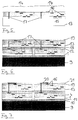
- a first component substrate 1 made of, for example, monocrystalline silicon comprises a plurality of, usually identical, chips 2 arranged according to a defined scheme, the circuit structures 3, such as a MOS transistor, and contain one or more metallization levels 4, which typically consist of aluminum, an aluminum alloy or other materials, such as copper or tungsten, and for electrical insulation are surrounded by an oxide layer 5, which can also be doped with boron and / or phosphorus for planarization purposes .
- the top metallization level 4 can also be covered by a passivation layer 6 made of, for example, silicon oxide and silicon nitride.
- adjustment structures for the precise joining of several levels are implemented (not shown in FIG. 1).
- the substrate has a thickness of, for example, 625 ⁇ m. This component substrate represents the lower substrate of the multilayer system (FIG. 1).
- the passivation 6 is opened at the top metallization level at certain measuring points.
- the individual chips of the substrate are then subjected to a functional test and the defective chips are identified (e.g. with an inkjet).
- a passivation layer is then applied again in order to protect the exposed measuring points again.
- This adhesive layer 7 with a thickness of typically 1-2 ⁇ m can also cause a planarization of the surface.
- the auxiliary substrate 8 is used as a handling substrate for the further process steps and protects the surface of the component substrate 1 during further processing. (Fig. 2).
- the component substrate 1 is thinned from the back by etching and / or grinding, so that the thickness of the substrate 1 below the circuit structures 3 is only a few micrometers, typically 1-5 ⁇ m, is. The selected remaining thickness also depends on the type of circuits contained.
- a carrier substrate 9, e.g. consists of mono- or polycrystalline silicon and possibly covered with an insulation layer 10, such as silicon oxide, does not contain any circuit structures.
- the component substrate 1 with the handling substrate 8 is divided into individual chips. This can be done with an etching process, by sawing or with a laser.
- the marked, intact chips 2 are then applied next to one another in a predetermined arrangement on the carrier substrate 9.
- the handling substrate 8 is then removed by etching or grinding, and the exposed adhesive layer 7 is typically removed over the entire area using an oxygen plasma or a solvent.
- the surface of the carrier substrate 9 with the component substrates 1 now has trenches between the individual chips 2 which have a very low aspect ratio.
- the layer 12 e.g. CVD oxide
- the passivation layer 6 can serve as a stop layer for the etching back or grinding back.
- the carrier substrate 9 with the applied first component level can now be further processed like a conventional silicon substrate with standard technology devices (FIG. 4).
- a second component substrate 13 likewise comprises a plurality of, usually identical, chips 14 arranged according to a defined scheme, which contain circuit structures 15, such as a MOS transistor, and one or more metallization levels 16.
- This substrate 13 is constructed essentially similarly to the first component substrate 1, but the circuit structures 15 are generally different in their function.
- the second component substrate has via holes 17 at the locations on which the electrical contact to the underlying circuit structures is to be made later. The via holes 17 are so deep that they extend to below the layer with circuit structures 15 (FIG. 5).
- This component substrate 13 is also subjected to a functional test, the defective chips are identified, and an adhesive layer and an auxiliary substrate are applied in a similar manner.
- the component substrate 13 is likewise thinned from the back to the via holes 17 by etching and / or grinding.
- the second component substrate 13 with the handling substrate is now divided into individual chips and the marked, intact chips 14 are aligned on the carrier substrate 9, provided with an adhesive layer 18, with the first component level 1.
- the adhesive layer 18 with a thickness of typically 1-2 ⁇ m can cause a planarization of the surface.
- the handling substrate is then removed by etching or grinding and the exposed adhesive layer is removed over the entire surface. Then, after layer 19 has been deposited (for example CVD oxide), a planarization step is also carried out, with which a flat surface is produced (FIG. 6).
- the vertical connection 20 is established between a metallization level 16 of the upper component level (substrate 13) and a metallization level 4 of the lower component level (substrate 1).
- a contact hole to a metallization level 16 of the upper component level and the prepared via holes 17 to a metallization level 4 of the lower component level are opened with a photolithography step and an electrical connection 20 is realized by metal deposition and structuring.
- a passivation layer 21 is deposited on the surface (FIG. 7).
- the electrical contact can of course also be implemented in a different way, for example when the chips are being applied to the lower substrate by means of prepared front and rear contacts (cf. introduction to the description: Y. Hayashi et al.).
- the already implemented system consisting of two layers is subjected to a function test and the defective chips are identified.
- a passivation layer is then deposited over the entire surface to protect the surface.
- An adhesive layer 22 and an auxiliary substrate 23 are then applied in the manner already illustrated.
- the carrier substrate 9 including the insulation layer 10 and the adhesive layer 11 under the first component level (substrate 1) are finally z. B. removed by etching and / or grinding from the back (Fig. 8).
- the carrier substrate can also be removed, for example, by etching away the adhesive layer 11 and then used again as a carrier substrate for subsequent process steps (claim 4).
- the auxiliary substrate 23 is now divided into individual chips (partial stacks) 24 together with the two component levels, whereupon the marked, intact chips are adjusted and applied to a new carrier substrate 26, which may be provided with an insulation layer 27 and with an adhesive layer 28 (FIG . 9).
- the handling substrates 25 are then removed by etching and / or grinding and the exposed adhesive layer 22 is removed over the entire area. Then, after layer 29 (e.g. CVD oxide) has been deposited, a planarization step is also carried out, with which a flat surface is produced. A substrate is thus obtained which contains only fully functional chips with two component levels (FIG. 10).
- layer 29 e.g. CVD oxide
Abstract
Description
Die Erfindung betrifft ein Verfahren zur Herstellung einer dreidimensionalen integrierten Schaltung unter Erreichung hoher Systemausbeuten. Unter dreidimensionaler Integration versteht man die vertikale Verbindung von Bauelementen, die mittels Planartechnik hergestellt wurden. Die Vorteile eines dreidimensional integrierten mikroelektronischen Systems sind u.a. die bei gleichen Designregeln erreichbaren höheren Packungsdichten und Schaltgeschwindigkeiten gegenüber zweidimensionalen Systemen. Letzteres ist zum einen bedingt durch kürzere Leitungswege zwischen den einzelnen Bauelementen oder Schaltungen, zum anderen durch die Möglichkeit der parallelen Informationsverarbeitung. Die Steigerung der Leistungsfähigkeit des Systems ist bei Realisierung einer Verbindungstechnik mit örtlich frei wählbaren höchstintegrierbaren vertikalen Kontakten optimal.The invention relates to a method for producing a three-dimensional integrated circuit while achieving high system yields. Three-dimensional integration is the vertical connection of components that were manufactured using planar technology. The advantages of a three-dimensionally integrated microelectronic system include the higher packing densities and switching speeds that can be achieved with the same design rules compared to two-dimensional systems. The latter is due, on the one hand, to shorter line paths between the individual components or circuits, and, on the other hand, to the possibility of parallel information processing. The increase in the performance of the system is optimal when implementing a connection technology with freely selectable, highly integrable vertical contacts.
Zur Herstellung dreidimensionaler Schaltungsanordnungen mit frei wählbaren vertikalen Kontakten sind folgende Verfahren bekannt:
Y. Akasaka, Proc. IEEE 74 (1986) 1703, schlägt vor, auf eine fertig prozessierte Bauelementeschicht polykristallines Silizium abzuscheiden und zu rekristallisieren, so daß in der rekristallisierten Schicht weitere Bauelemente gefertigt werden können. Nachteile dieser Methode sind die ausbeutereduzierende Degradation der Bauelemente in der unteren Ebene durch die hohe thermische Belastung beim Rekristallisierungsprozeß, sowie die notwendigerweise serielle Prozessierung des Gesamtsystems. Letzteres bedingt zum einen entsprechend lange Durchlaufzeiten bei der Fertigung und hat zum anderen eine Ausbeuteminderung durch Aufsummierung der prozeßbedingten Ausfälle zur Folge. Beides erhöht die Fertigungskosten beträchtlich gegenüber einer Prozessierung der einzelnen Ebenen getrennt voneinander in verschiedenen Substraten.The following methods are known for producing three-dimensional circuit arrangements with freely selectable vertical contacts:
Y. Akasaka, Proc. IEEE 74 (1986) 1703, proposes to deposit and recrystallize polycrystalline silicon on a completely processed component layer, so that further components can be produced in the recrystallized layer. Disadvantages of this method are the yield-reducing degradation of the components in the lower level due to the high thermal load during the recrystallization process, and the necessary serial processing of the overall system. The latter, on the one hand, necessitates correspondingly long throughput times in production and, on the other hand, results in a reduction in yield by adding up the process-related failures. Both increase the manufacturing costs considerably compared to processing the individual levels separately from one another in different substrates.
Aus Y. Hayashi et al., Proc. 8th Int. Workshop on Future Electron Devices, 1990, p. 85, ist es bekannt, zunächst die einzelnen Bauelementeebenen getrennt voneinander in verschiedenen Substraten herzustellen. Anschließend werden die Substrate auf wenige Mikrometer gedünnt, mit Vorder- und Rückseitenkontakten versehen und mittels eines Bondverfahrens vertikal verbunden. Für die Bereitstellung der Vorder- und Rückseitenkontakte sind jedoch Sonderprozesse notwendig sind, die in der Standard - Halbleiterfertigung (CMOS) nicht vorgesehen sind, nämlich MOS - inkompatible Materialien (z.B. Gold) und Rückseitenstrukturierung des Substrates.From Y. Hayashi et al., Proc. 8th Int. Workshop on Future Electron Devices, 1990, p. 85, it is known to first produce the individual component levels separately from one another in different substrates. The substrates are then thinned to a few micrometers, provided with front and rear contacts and connected vertically by means of a bonding process. For the provision of the front and back contacts, however, special processes are required that are not provided for in standard semiconductor manufacturing (CMOS), namely MOS - incompatible materials (e.g. gold) and rear structuring of the substrate.
Die US 4,939,568 beschreibt ein Verfahren zur Herstellung einer dreidimensionalen integrierten Schaltungsstruktur durch Stapelung einzelner ICs zu einem Einzelchipstapel auf einem Trägersubstrat. Hierzu wird zunächst ein Substrat mit fertigprozessierten ICs in einzelne Chips unterteilt, womit die Prozessierung auf Waferebene beendet ist. Die Chips werden getestet, und ein erster einzelner Chip wird mittels Thermokompression auf ein Trägersubstrat aufgebracht. Nach diesem Schritt wird ein weiterer Chip in der gleichen Weise auf den ersten Chip aufgebracht. Es wird somit zunächst ein erster Chipstapel fertiggestellt, bevor mit der Herstellung eines weiteren Chipstapels auf einem anderen Trägersubstrat begonnen wird. Eine Weiterprozessierung der Chipstapel auf Waferebene ist mit diesem Verfahren daher nicht möglich.No. 4,939,568 describes a method for producing a three-dimensional integrated circuit structure by stacking individual ICs to form a single chip stack on a carrier substrate. For this purpose, a substrate with finished ICs is first divided into individual chips, which ends the processing at the wafer level. The chips are tested and a first single chip is applied to a carrier substrate by means of thermal compression. After this step, another chip is applied to the first chip in the same way. A first chip stack is thus first completed before the production of a further chip stack on another carrier substrate is started. Further processing of the chip stack at the wafer level is therefore not possible with this method.
Ein wesentlicher Nachteil der bisher genannten Verfahren ist dadurch bedingt, daß die in der Siliziumtechnologie zur Verfügung stehenden Geräte nur eine Bearbeitung (Prozessierung) von scheibenförmigen Substraten, den sog. Wafern, zulassen. Eine Prozessierung davon verschiedener Substrate, insbesondere von einzelnen Chips, ist nur in experimentellen Versuchsanlagen möglich, jedoch nicht im Rahmen einer industriellen Fertigung mit den geforderten hohen Ausbeuten.A major disadvantage of the previously mentioned methods is due to the fact that the devices available in silicon technology only allow processing (processing) of disk-shaped substrates, the so-called wafers. A processing of different substrates, especially of individual chips, is only possible in experimental test plants, but not in the context of industrial production with the required high yields.
Die US 4,954,875 beschreibt ein Verfahren zur dreidimensionalen Integration durch Stapelung einzelner Wafer, bei dem die Verbindung der einzelnen Bauelementeebenen über besonders geformte Vias hergestellt wird. Beim Zusammenfügen von Substraten, die eine Vielzahl von identischen Bausteinen, den sog. Chips, enthalten, ergibt sich die resultierende Ausbeute eines mehrlagigen Systems aus dem Produkt der Einzelausbeuten. Dies führt dazu, daß die Ausbeute eines mehrere Bauelementeebenen umfassenden Systems, wie das der US 4,954,875 nach den bekannten Verfahren drastisch abnimmt. So erhält man bei einer Ausbeute einer Einzelebene von 80 % bei einem Gesamtsystem aus 10 Ebenen nur mehr eine resultierende Gesamtausbeute von etwa 10 %, womit ein derartiges System unwirtschaftlich wird und der Einsatz dieser Technik auf wenige spezielle Einsatzfelder beschränkt wird. Die Ausbeute eines Bauelementesubstrates hängt dabei auch von der Art der Schaltungen und des verwendeten Herstellungsprozesses ab. So erzielt man z.B. in der Fertigung von Speicherbausteinen sehr hohe Ausbeuten, während bei Logikbausteinen, wie Mikroprozessoren, eine deutlich geringere Ausbeute erreicht wird. Insbesondere wenn mehrere Arten solcher Schaltungen übereinandergestapelt werden, wird damit die Gesamtausbeute überproportional durch die Schaltungsart mit der geringsten Ausbeute bestimmt.No. 4,954,875 describes a method for three-dimensional integration by stacking individual wafers, in which the connection of the individual component levels is established via specially shaped vias. When substrates that contain a large number of identical building blocks, the so-called chips, are joined together, the resultant yield of a multilayer system results from the product of the individual yields. As a result, the yield of a system comprising several component levels, such as that of US Pat. No. 4,954,875, drops drastically according to the known processes. With a yield of a single level of 80% for a total system of 10 levels, the result is a total yield of about 10%, making such a system uneconomical and restricting the use of this technology to a few special fields of application. The yield of a component substrate also depends on the type of circuits and the manufacturing process used. For example, very high yields in the production of memory chips, while a significantly lower yield is achieved with logic chips, such as microprocessors. In particular, if several types of such circuits are stacked on top of one another, the overall yield is determined disproportionately by the type of circuit with the lowest yield.
Der Erfindung liegt die Aufgabe zugrunde, ein Verfahren zur Herstellung einer dreidimensionalen integrierten Schaltung anzugeben, mit dem unter Verwendung der üblichen industriellen Standardausrüstung auf Waferebene eine deutliche Ausbeutesteigerung gegenüber bisher bekannten Verfahren erzielt wird.The invention is based on the object of specifying a method for producing a three-dimensional integrated circuit with which a clear increase in yield compared to previously known methods is achieved using the usual industrial standard equipment at the wafer level.
Diese Aufgabe wird erfindungsgemäß mit dem Verfahren nach Anspruch 1 gelöst. Besondere Ausgestaltungen des Verfahrens sind Gegenstand der Unteransprüche.This object is achieved with the method according to
In dem erfindungsgemäßen Verfahren wird zum Aufbau eines mehrere Bauelementeebenen umfassenden Systems ein zusätzliches Trägersubstrat verwendet, das keine Bauelementestrukturen enthalt. Ein fertig prozessiertes Substrat, das Schaltungsstrukturen und Metallisierungsebenen umfaßt, wird einem Funktionstest unterzogen, mit dem die intakten Chips des Substrates selektiert werden. Anschließend wird dieses Substrat mit einem Hilfssubstrat verbunden, von der Rückseite her gedünnt und in einzelne Chips zerlegt. Statt des Dünnens des Substrates bis nahe an die Bauelementestrukturen heran kann auch im Falle eines SOI-Substrates der Substratbereich unterhalb der Oxidschicht entfernt werden. Dann werden selektierte, intakte Chips mit dem Trägersubstrat, beispielsweise über eine Haftschicht, verbunden, wobei die Anordnung der Einzelchips nebeneinander in einem vorgegebenen Schema erfolgt. Die Chips werden somit auf dem Trägersubstrat zu einer neuen Chipebene zusammengesetzt. Auf diese Weise wird ein Wafer bereitgestellt, der in der Bauelementeebene nur intakte Bauelemente und Schaltkreise enthält. Schließlich wird das (zerteilte) Hilfssubstrat entfernt.In the method according to the invention, an additional carrier substrate which does not contain any component structures is used to build up a system comprising a plurality of component levels. A fully processed substrate, which comprises circuit structures and metallization levels, is subjected to a functional test with which the intact chips of the substrate are selected. This substrate is then connected to an auxiliary substrate, thinned from the rear and broken down into individual chips. Instead of thinning the substrate close to the component structures, the substrate region below the oxide layer can also be removed in the case of an SOI substrate. Selected, intact chips are then connected to the carrier substrate, for example via an adhesive layer, the individual chips being arranged next to one another in a predetermined scheme. The chips are thus assembled on the carrier substrate to form a new chip level. In this way, a wafer is provided which contains only intact components and circuits in the component level. Finally, the (divided) auxiliary substrate is removed.
Da auf dem Trägersubstrat nun einzelne Chips aufgebracht worden sind, ist keine zusammenhängende Oberfläche mehr vorhanden (Gräben zwischen den Chips), so daß bestimmte Prozeßschritte, insbesondere Photolithographiemodule, nicht mehr mit hoher Ausbeute durchgeführt werden können. Deshalb wird nun vorzugsweise ein Planarisierungsschritt eingefügt (Anspruch 9). Danach kann das Substrat, das in der Bauelementeebene nur noch getestete und funktionsfähige Chips enthält, in gängigen Fertigungsanlagen weiter verarbeitet werden.Since individual chips have now been applied to the carrier substrate, there is no longer any coherent surface (trenches between the chips), so that certain process steps, in particular photolithography modules, can no longer be carried out with a high yield. Therefore, a planarization step is now preferably inserted (claim 9). After that, the substrate, which only contains tested and functional chips in the component level, can be processed further in common manufacturing plants.
Die Planarisierung kann mit verschiedenen Verfahren durchgeführt werden. Dabei wird zuerst eine Isolationsschicht, wie z. B. Spin-on-Glas oder ein CVD - Oxid, aufgebracht, um die Gräben aufzufüllen. Anschließend wird die Oberfläche eingeebnet, was durch Rückätzen, mechanisches oder chemomechanisches Schleifen erfolgt.The planarization can be carried out using various methods. First, an insulation layer, such as. B. spin-on glass or a CVD oxide, applied to fill the trenches. The surface is then leveled, which is done by etching back, mechanical or chemomechanical grinding.
Weitere Prozesse, die nicht auf Chipebene realisierbar sind, können nun nach dem Planarisierungsschritt problemlos an dem Trägersubstrat mit vorselektierten Chips durchgeführt werden.Further processes that cannot be implemented at the chip level can now be carried out without problems on the carrier substrate with pre-selected chips after the planarization step.
Nach Fertigstellung der ersten Bauelementeebene wird eine weitere Bauelementeebene z.B. in der gleichen Weise chipweise aufgebracht und die Oberfläche planarisiert (Anspruch 2).
Anschließend wird z.B. über Vialöcher (Anspruch 10), die bereits bei der Prozessierung der Einzelsubstrate in die Chips eingebracht wurden und nun bis zu einer Metallisierungsebene der darunterliegenden Bauelementeebene durchgeätzt werden, die elektrische Verbindung zwischen je einer Metallisierung der oberen und der unteren Bauelementeebene hergestellt. Dabei wird die Photomaske zur Strukturierung auf jeden einzelnen Chip über Justierstrukturen separat justiert, um etwaige Maßabweichungen durch das Aufbringen der einzelnen Chips auszugleichen und eine hohe Justiergenauigkeit zu erreichen.After completion of the first component level, a further component level is applied, for example in the same way, in chips and the surface is planarized (claim 2).
The electrical connection between a metallization of the upper and lower component levels is then established, for example, via vias (claim 10), which were already introduced into the chips during the processing of the individual substrates and are now etched through to a metallization level of the component level below. The structuring of the photomask on each individual chip is adjusted separately using adjustment structures in order to compensate for any dimensional deviations caused by the application of the individual chips and to achieve high adjustment accuracy.
Soll zusätzlich eine weitere Bauelementeebene aufgebracht werden (Anspruch 3), so wird der vorhandene Teilstapel (d.h. das ursprüngliche Trägersubstrat mit sämtlichen bisher aufgebrachten Bauelementeebenen) auf seine Funktionsweise getestet, mit einem Hilfssubstrat versehen, das ursprüngliche Trägersubstrat entfernt, und das Hilfssubstrat mit den Bauelementeebenen in Chips vereinzelt. Die funktionsfähigen Chips werden über eine Haftschicht mit einem neuen Trägersubstrat verbunden, die Hilfssubstrate entfernt und eine Planarisierung der Oberfläche durchgeführt. Dann wird in gleicher Weise eine weitere Bauelementeebene chipweise aufgebracht, die Oberfläche planarisiert und die elektrische Verbindung hergestellt.If an additional component level is to be applied (claim 3), the existing partial stack (i.e. the original carrier substrate with all previously applied component levels) is tested for its functionality, provided with an auxiliary substrate, the original carrier substrate removed, and the auxiliary substrate with the component levels in Chips isolated. The functional chips are connected to a new carrier substrate via an adhesive layer, the auxiliary substrates are removed and the surface is planarized. Then, in the same way, a further component level is applied in chips, the surface is planarized and the electrical connection is established.
Die Anzahl der Ebenen, die aufgebracht werden, ist bei diesem Verfahren nicht beschränkt. Außerdem kann nicht nur eine Einzelebene, sondern auch ein bereits aus mehreren Ebenen bestehender Teilstapel chipweise aufgebracht werden.The number of levels that are applied is not limited in this method. In addition, not only a single level, but also a partial stack that already consists of several levels can be applied in chips.
Als Substrate sind monokristalline Siliziumsubstrate, SOI - Substrate oder Substrate verschiedener Technologiefamilien, wie z.B. III - V - Halbleiter geeignet. Als Trägersubstrat sind neben mono- oder polykristallinen Siliziumsubstraten, die mit einer Isolationsschicht, wie z.B. Siliziumoxid, versehen sein können, auch andere Materialien verwendbar, die zu Halbleiterprozessen kompatibel sind, wie z.B. Quarz- oder Glassubstrate. Von Vorteil ist es dabei, wenn die thermischen Ausdehnungskoeffizienten von Trägersubstrat und Bauelementesubstrat angepaßt sind, um mechanische Spannungen aufgrund von durch Prozeßschritte bedingte Temperaturzyklen gering zu halten. Da die verwendeten Bauelementesubstrate bereits Metallisierungsebenen umfassen, die üblicherweise Aluminium oder eine Aluminiumlegierung enthalten, sind die nachfolgenden Prozeßschritte in der Regel auf maximale Temperaturen von etwa 400°C beschränkt. Zusätzlich kann die Haftschicht als Pufferschicht zum Abbau von mechanischem Streß oder als Passivierungsschicht (Anspruch 7) fungieren. Weiterhin kann die Haftschicht eine Planarisierung der Oberfläche bewirken (Anspruch 8). Als Haftschicht kann dabei ein organisches Material, wie z.B. Polyimid oder Photolack verwendet werden.Monocrystalline silicon substrates, SOI substrates or substrates of different technology families, such as e.g. III - V semiconductors suitable. In addition to monocrystalline or polycrystalline silicon substrates, which are provided with an insulating layer, such as e.g. Silicon oxide can be provided, other materials that are compatible with semiconductor processes, such as e.g. Quartz or glass substrates. It is advantageous if the thermal expansion coefficients of the carrier substrate and the component substrate are adapted in order to keep mechanical stresses low due to temperature cycles caused by process steps. Since the component substrates used already comprise metallization levels which usually contain aluminum or an aluminum alloy, the subsequent process steps are generally restricted to maximum temperatures of approximately 400 ° C. In addition, the adhesive layer can function as a buffer layer for reducing mechanical stress or as a passivation layer (claim 7). Furthermore, the adhesive layer can bring about a planarization of the surface (claim 8). An organic material such as e.g. Polyimide or photoresist can be used.
Insgesamt werden bei diesem Verfahren zur Herstellung einer dreidimensionalen integrierten Schaltung nur bekannte und eingeführte Verfahrensschritte verwendet, so daß keine neuen Prozesse entwickelt werden müssen.
Das erfindungsgemäße Verfahren eignet sich hervorragend zum Aufbau von mehrlagigen Systemen. Da beim dem Verfahren nur vorgetestete Elemente verwendet und nur funktionsfähige Teilstapel weiter verarbeitet werden, wird vermieden, daß funktionsfähige Chips auf bereits defekte Bauelementestapel aufgebracht und damit wertlos werden. Dadurch erhöht sich in vorteilhafter Weise die Gesamtausbeute des Systems, so daß eine deutliche Kostenreduktion zu erzielen ist.Overall, only known and introduced method steps are used in this method for producing a three-dimensional integrated circuit, so that no new processes have to be developed.
The method according to the invention is excellently suited for the construction of multilayer systems. Since only pretested elements are used in the method and only functional partial stacks are processed further, it is avoided that functional chips are applied to already defective component stacks and are thus worthless. This increases the overall yield of the system in an advantageous manner, so that a significant cost reduction can be achieved.
Im folgenden wird die Erfindung anhand der Zeichnungen und eines Ausführungsbeispiels näher erläutert.The invention is explained in more detail below with reference to the drawings and an exemplary embodiment.
Dabei zeigen:
- Fig. 1
- ein erstes Bauelementesubstrat mit Schaltungsstrukturen und Metallisierungsebenen,
- Fig. 2
- das erste Bauelementesubstrat mit Haftschicht und Hilfssubstrat,
- Fig. 3
- ein Trägersubstrat mit Haftschicht,
- Fig. 4
- ein Trägersubstrat mit einer chipweise aufgebrachten ersten Bauelementeebene nach Planarisierung der Oberfläche,
- Fig. 5
- ein zweites Bauelementesubstrat mit Schaltungsstrukturen und Metallisierungsebenen,
- Fig. 6
- ein Trägersubstrat mit zwei chipweise aufgebrachten Bauelementeebenen nach Planarisierung der Oberfläche,
- Fig. 7
- ein Trägersubstrat mit zwei vertikal verbundenen Bauelementeebenen,
- Fig. 8
- ein Hilfssubstrat mit zwei vertikal verbundenen Bauelementeebenen nach Entfernen des Trägersubstrates,
- Fig. 9
- ein Trägersubstrat mit zwei chipweise aufgebrachten Bauelementestapeln aus zwei Bauelementeebenen mit den Hilfssubstraten, und
- Fig. 10
- ein Trägersubstrat mit zwei chipweise aufgebrachten Bauelementestapeln aus zwei Bauelementeebenen nach Planarisierung der Oberfläche.
- Fig. 1
- a first component substrate with circuit structures and metallization levels,
- Fig. 2
- the first component substrate with adhesive layer and auxiliary substrate,
- Fig. 3
- a carrier substrate with an adhesive layer,
- Fig. 4
- a carrier substrate with a first component level applied in chips after planarization of the surface,
- Fig. 5
- a second component substrate with circuit structures and metallization levels,
- Fig. 6
- a carrier substrate with two component layers applied in chips after planarization of the surface,
- Fig. 7
- a carrier substrate with two vertically connected component levels,
- Fig. 8
- an auxiliary substrate with two vertically connected component levels after removal of the carrier substrate,
- Fig. 9
- a carrier substrate with two chip-stacked component stacks from two component levels with the auxiliary substrates, and
- Fig. 10
- a carrier substrate with two stacked component stacks from two component levels after planarization of the surface.
Ein erstes Bauelementesubstrat 1 aus z.B. monokristallinem Silizium umfaßt mehrere, nach einem definierten Schema angeordnete, üblicherweise identische Chips 2, die Schaltungsstrukturen 3, wie beispielsweise einen MOS - Transistor, und eine oder mehrere Metallisierungsebenen 4 enthalten, die typischerweise aus Aluminum, einer Aluminiumlegierung oder anderen Materalien, wie Kupfer oder Wolfram, bestehen und zur elektrischen Isolation von einer Oxidschicht 5, die zu Planarisierungszwecken auch mit Bor und/oder Phosphor dotiert sein kann, umgeben sind. Die oberste Metallisierungsebene 4 kann dabei auch von einer Passivierungsschicht 6 aus beispielsweise Siliziumoxid und Siliziumnitrid bedeckt sein. Weiterhin sind Justagestrukturen zum genauen Zusammenfügen mehrerer Ebenen implementiert (in Fig. 1 nicht gezeigt). Unterhalb der Schaltungsstrukturen 3 weist das Substrat eine Dicke von z.B. 625 µm auf. Dieses Bauelementesubstrat stellt das untere Substrat des mehrlagigen Systems dar (Fig. 1).A
Nach Fertigstellung des Bauelementesubstrates 1 wird die Passivierung 6 auf der obersten Metallisierungsebene an bestimmten Meßstellen geöffnet. Danach werden die einzelnen Chips des Substrates einem Funktionstest unterzogen und die defekten Chips gekennzeichnet (z.B. mit einem Tintenstrahl). Anschließend wird erneut eine Passivierungsschicht aufgebracht, um die offenliegenden Meßstellen wieder zu schützen.After completion of the
Auf die Oberfläche des Substrates 1 wird ganzflächig eine Haftschicht 7 aus einem organischen Material, wie Polyimid oder Photolack, aufgebracht. Diese Haftschicht 7 mit einer Dicke von typischerweise 1 - 2 µm kann außerdem eine Planarisierung der Oberfläche bewirken. Auf die Haftschicht 7 wird schließlich ein Hilfssubstrat 8, wie beispielsweise ein Silizium- oder Quarzwafer, geklebt. Das Hilfssubstrat 8 wird als Handlingsubstrat für die weiteren Prozeßschritte verwendet und schützt die Oberfläche des Bauelementesubstrates 1 bei der weiteren Bearbeitung. (Fig. 2).An adhesive layer 7 made of an organic material, such as polyimide or photoresist, is applied to the entire surface of the
Danach wird das Bauelementesubstrat 1 durch Ätzen und/oder Schleifen von der Rückseite her gedünnt, so daß die Dicke des Substrates 1 unterhalb der Schaltungsstrukturen 3 nur noch wenige Mikrometer, typischerweise 1 - 5 µm, beträgt. Dabei hängt die gewählte Restdicke auch von der Art der enthaltenen Schaltungen ab.Thereafter, the
Ein Trägersubstrat 9, das z.B. aus mono- oder polykristallinem Silizium besteht und eventuell mit einer Isolationsschicht 10, wie Siliziumoxid, bedeckt ist, enthält keine Schaltungsstrukturen. Auf dieses Trägersubstrat 9 wird nun eine Haftschicht 11 aus z.B. Polyimid oder Photolack, aufgebracht (Fig. 3).A
Nun wird das Bauelementesubstrat 1 mit dem Handlingsubstrat 8 in einzelne Chips zerteilt. Dies kann dabei mit einem Ätzprozeß, durch Sägen oder mit einem Laser erfolgen. Daraufhin werden die gekennzeichneten, intakten Chips 2 auf das Trägersubstrat 9 in einer vorgegebenen Anordnungweise nebeneinander aufgebracht. Anschließend wird das Handlingsubstrat 8 durch Abätzen oder Abschleifen entfernt und die freiliegende Haftschicht 7 typischerweise mit einem Sauerstoffplasma oder einem Lösungsmittel ganzflächig entfernt. Nach dem Aufkleben der Chips 2 weist die Oberfläche des Trägersubstrates 9 mit den Bauelementsubstraten 1 nun Gräben zwischen den einzelnen Chips 2 auf, die ein sehr niedriges Aspektverhältnis besitzen. Durch einen Planarisierungsschritt, bei dem die Schicht 12 (z.B. CVD-Oxid) abgeschieden wird, werden diese Gräben nun aufgefüllt und eine ebene Oberfläche erzeugt. Dabei kann die Passivierungsschicht 6 als Stoppschicht für das Rückätzen bzw. Rückschleifen dienen. Das Trägersubstrat 9 mit der aufgebrachten ersten Bauelementeebene läßt sich nun wie ein übliches Siliziumsubstrat mit Standard - Technologiegeräten weiterverarbeiten (Fig. 4).Now the
Ein zweites Bauelementesubstrat 13 umfaßt ebenfalls mehrere, nach einem definierten Schema angeordnete, üblicherweise identische Chips 14, die Schaltungsstrukturen 15, wie beispielsweise einen MOS - Transistor, und eine oder mehrere Metallisierungsebenen 16 enthalten. Dieses Substrat 13 ist im wesentlichen ähnlich aufgebaut wie das erste Bauelementesubstrat 1, die Schaltungsstrukturen 15 sind aber in der Regel von ihrer Funktion her unterschiedlich. Desweiteren weist das zweite Bauelementesubstrat Vialöcher 17 an den Stellen auf, an denen später die elektrische Kontaktierung zu darunterliegenden Schaltungsstrukturen erfolgen soll. Die Vialöcher 17 sind so tief, daß sie bis unterhalb der Schicht mit Schaltungsstrukturen 15 reichen (Fig. 5).
Auch dieses Bauelementesubstrat 13 wird einem Funktionstest unterzogen, die defekten Chips werden gekennzeichnet, und eine Haftschicht und ein Hilfssubstrat werden in ähnlicher Vorgehensweise aufgebracht. Schließlich wird das Bauelementesubstrat 13 ebenfalls durch Ätzen und / oder Schleifen von der Rückseite her bis an die Vialöcher 17 heran gedünnt. Das zweite Bauelementesubstrat 13 mit dem Handlingsubstrat wird nun in einzelne Chips zerteilt und die gekennzeichneten, intakten Chips 14 werden justiert auf das, mit einer Haftschicht 18 versehene, Trägersubstrat 9 mit der ersten Bauelementeebene 1 aufgebracht. Die Haftschicht 18 mit einer Dicke von typischerweise 1 - 2 µm kann dabei eine Planarisierung der Oberfläche bewirken. Anschließend wird das Handlingsubstrat durch Abätzen oder Abschleifen abgetragen und die freiliegende Haftschicht ganzflächig entfernt. Daraufhin wird nach Abscheidung der Schicht 19 (z.B. CVD-Oxid), ebenfalls ein Planarisierungsschritt durchgeführt, mit dem eine ebene Oberfläche erzeugt wird (Fig. 6).A
This
Danach wird schließlich die vertikale Verbindung 20 zwischen einer Metallisierungsebene 16 der oberen Bauelementeebene (Substrat 13) und einer Metallsierungsebene 4 der unteren Bauelementeebene (Substrat 1) hergestellt. Dazu werden mit einem Photolithographieschritt ein Kontaktloch zu einer Metallisierungsebene 16 der oberen Bauelementeebene und die vorbereiteten Vialöcher 17 bis zu einer Metallisierungsebene 4 der unteren Bauelementeebene geöffnet und durch Metallabscheidung und Strukturierung eine elektrische Verbindung 20 realisiert. Schließlich wird auf die Oberfläche noch eine Passivierungsschicht 21 abgeschieden (Fig. 7).Finally, the
Die elektrische Kontaktierung kann selbstverständlich auch auf andere Weise realisiert werden, so z.B. bereits beim Aufbringen der Chips auf das untere Substrat mittels vorbereiteter Vorder- und Rückseitenkontakte (vgl. Beschreibungseinleitung: Y. Hayashi et al.).The electrical contact can of course also be implemented in a different way, for example when the chips are being applied to the lower substrate by means of prepared front and rear contacts (cf. introduction to the description: Y. Hayashi et al.).
Soll nun eine weitere Bauelementeebene aufgebracht werden, so wird das bereits realisierte System aus zwei Lagen einem Funktionstest unterzogen und die defekten Chips werden gekennzeichnet. Nachfolgend wird eine Passivierungsschicht ganzflächig abgeschieden, um die Oberfläche zu schützen. Daraufhin wird in der bereits dargestellten Weise eine Haftschicht 22 und ein Hilfssubstrat 23 aufgebracht. Das Trägersubstrat 9 einschließlich der Isolationsschicht 10 und die Haftschicht 11 unter der ersten Bauelementeebene (Substrat 1) werden schließlich z. B. durch Ätzen und / oder Schleifen von der Rückseite her entfernt (Fig. 8).
Das Trägersubstrat kann z.B. auch durch Wegätzen der Haftschicht 11 entfernt werden und dann erneut als Trägersubstrat für nachfolgende Prozeßschritte eingesetzt werden (Anspruch 4).If a further component level is now to be applied, the already implemented system consisting of two layers is subjected to a function test and the defective chips are identified. A passivation layer is then deposited over the entire surface to protect the surface. An
The carrier substrate can also be removed, for example, by etching away the
Nun wird das Hilfssubstrat 23 zusammen mit den beiden Bauelementeebenen in einzelne Chips (Teilstapel) 24 zerteilt, woraufhin die gekennzeichneten, intakten Chips justiert auf ein neues Trägersubstrat 26, das eventuell mit einer Isolationsschicht 27 und mit einer Haftschicht 28 versehen ist, aufgebracht werden (Fig. 9).The
Anschließend werden die Handlingsubstrate 25 (zerteiltes Handlingsubstrat 23) durch Abätzen und / oder Abschleifen abgetragen und die freiliegende Haftschicht 22 ganzflächig entfernt. Danach wird nach Abscheiden der Schicht 29 (z.B. CVD-Oxid) ebenfalls ein Planarisierungsschritt durchgeführt, mit dem eine ebene Oberfläche erzeugt wird. Damit erhält man ein Substrat, welches nur voll funktionsfähige Chips mit zwei Bauelementeebenen enthält (Fig. 10).The handling substrates 25 (divided handling substrate 23) are then removed by etching and / or grinding and the exposed
In ähnlicher Weise können weitere Bauelementeebenen hinzugefügt werden, wobei jeweils nur funktionsfähige Teilsysteme weiter verarbeitet werden.In a similar way, further component levels can be added, only functional subsystems being processed further.
Claims (14)
dadurch gekennzeichnet,
daß das Aufbringen der weiteren Bauelementeebene folgende Verfahrensschritte umfaßt:
characterized,
that the application of the further component level comprises the following process steps:
dadurch gekennzeichnet,
daß zum Aufbau einer dreidimensionalen integrierten Schaltung mit mehr als zwei Bauelementeebenen das Verfahren mehrmals nacheinander durchgeführt wird, wobei als erstes Substrat bei jeder wiederholten Durchführung des Verfahrens das Trägersubstrat mit den aufgebrachten Bauelementeebenen verwendet wird, das durch die jeweils vorhergehenden Verfahrensschritte bereitgestellt wird.The method of claim 1 or 2,
characterized,
that to build a three-dimensional integrated circuit with more than two component levels, the method is carried out several times in succession, with the carrier substrate with the applied component levels being used as the first substrate each time the method is carried out, which is provided by the respectively preceding method steps.
dadurch gekennzeichnet,
daß das gleiche Trägersubstrat mehrfach verwendet wird.Method according to claim 3,
characterized,
that the same carrier substrate is used several times.
dadurch gekennzeichnet,
daß das Hilfssubstrat über eine Haftschicht mit dem ersten und/oder dem zweiten Substrat verbunden wird.Method according to one of claims 1 to 4,
characterized,
that the auxiliary substrate is connected to the first and / or the second substrate via an adhesive layer.
dadurch gekennzeichnet,
daß die Chips mittels einer Haftschicht auf das Trägersubstrat oder auf Bauelementeebenen des Trägersubstrates aufgebracht werden.Method according to one of claims 1 to 5,
characterized,
that the chips are applied to the carrier substrate or to component levels of the carrier substrate by means of an adhesive layer.
dadurch gekennzeichnet,
daß eine Haftschicht mit passivierenden Eigenschaften verwendet wird.A method according to claim 5 or 6,
characterized,
that an adhesive layer with passivating properties is used.
dadurch gekennzeichnet,
daß eine Haftschicht verwendet wird, die eine Planarisierung der Oberfläche bewirkt.Method according to one of claims 5 to 7
characterized,
that an adhesive layer is used which causes planarization of the surface.
dadurch gekennzeichnet,
daß Gräben, die nach dem justierten Aufbringen der einzelnen Chips zwischen diesen entstehen, planarisiert werden.Method according to one of claims 1 to 8,
characterized,
that trenches that occur between the individual chips after the aligned application are planarized.
dadurch gekennzeichnet,
daß das Herstellen der elektrischen Kontakte zwischen den Bauelementen, Bauelementstapeln oder Schaltkreisen der aufgebrachten Chips und den Bauelementen, Bauelementstapeln oder Schaltkreisen des Trägersubstrates über Kontakt- und/oder Vialöcher (17) erfolgt.Method according to one of claims 2 to 9,
characterized,
that the electrical contacts between the components, component stacks or circuits of the applied chips and the components, component stacks or circuits of the carrier substrate are made via contact and / or via holes (17).
dadurch gekennzeichnet,
daß das Dünnen des ersten und/oder zweiten Substrates mittels Ätzen und/oder Schleifen erfolgt.Method according to one of claims 1 to 10,
characterized,
that the thinning of the first and / or second substrate takes place by means of etching and / or grinding.
dadurch gekennzeichnet,
daß das Entfernen des ersten und/oder zweiten Substrates und/oder des Hilfssubstrates durch Wegätzen einer Haftschicht zwischen dem jeweiligen Substrat und den Bauelementeebenen erfolgt.Method according to one of claims 1 to 11,
characterized,
that the removal of the first and / or second substrate and / or the auxiliary substrate is carried out by etching away an adhesive layer between the respective substrate and the component levels.
dadurch gekennzeichnet,
daß ein Trägersubstrat und/oder ein Hilfssubstrat aus Halbleitermaterial, Quarz oder Glas verwendet wird.Method according to one of claims 1 to 12,
characterized,
that a carrier substrate and / or an auxiliary substrate made of semiconductor material, quartz or glass is used.
dadurch gekennzeichnet,
daß ein SOI-Substrat als erstes und/oder als zweites Substrat verwendet wird.Method according to one of claims 1 to 13,
characterized,
that an SOI substrate is used as the first and / or as the second substrate.
Applications Claiming Priority (2)
| Application Number | Priority Date | Filing Date | Title |
|---|---|---|---|
| DE4433833 | 1994-09-22 | ||
| DE4433833A DE4433833A1 (en) | 1994-09-22 | 1994-09-22 | Method for producing a three-dimensional integrated circuit while achieving high system yields |
Publications (2)
| Publication Number | Publication Date |
|---|---|
| EP0703619A1 true EP0703619A1 (en) | 1996-03-27 |
| EP0703619B1 EP0703619B1 (en) | 1999-11-03 |
Family
ID=6528893
Family Applications (1)
| Application Number | Title | Priority Date | Filing Date |
|---|---|---|---|
| EP95113435A Expired - Lifetime EP0703619B1 (en) | 1994-09-22 | 1995-08-26 | Method for fabricating a three dimensional integrated circuit for a higher system gain achievement |
Country Status (4)
| Country | Link |
|---|---|
| US (1) | US5877034A (en) |
| EP (1) | EP0703619B1 (en) |
| JP (1) | JPH08204123A (en) |
| DE (2) | DE4433833A1 (en) |
Cited By (8)
| Publication number | Priority date | Publication date | Assignee | Title |
|---|---|---|---|---|
| WO1998002921A1 (en) * | 1996-07-11 | 1998-01-22 | Kopin Corporation | Transferred flexible integrated circuit |
| EP0975472A1 (en) * | 1997-04-04 | 2000-02-02 | Glenn J. Leedy | Three dimensional structure memory |
| WO2000074136A1 (en) * | 1999-05-31 | 2000-12-07 | Fraunhofer-Gesellschaft zur Förderung der angewandten Forschung e.V. | Method for producing three-dimensional circuits |
| WO2003041167A1 (en) * | 2001-11-05 | 2003-05-15 | Mitsumasa Koyanagi | Semiconductor device comprising low dielectric material film and its production method |
| DE10200399A1 (en) * | 2002-01-08 | 2003-07-24 | Advanced Micro Devices Inc | Three-dimensionally integrated semiconductor device |
| US7265402B2 (en) | 2001-11-05 | 2007-09-04 | Zycube Co., Ltd. | Solid-state image sensor including a microlens |
| US7670893B2 (en) | 1992-04-08 | 2010-03-02 | Taiwan Semiconductor Manufacturing Co., Ltd. | Membrane IC fabrication |
| US7705466B2 (en) | 1997-04-04 | 2010-04-27 | Elm Technology Corporation | Three dimensional multi layer memory and control logic integrated circuit structure |
Families Citing this family (186)
| Publication number | Priority date | Publication date | Assignee | Title |
|---|---|---|---|---|
| DE19516487C1 (en) * | 1995-05-05 | 1996-07-25 | Fraunhofer Ges Forschung | Vertical integration process for microelectronic system |
| DE19543540C1 (en) * | 1995-11-22 | 1996-11-21 | Siemens Ag | Vertically integrated semiconductor component |
| US6342434B1 (en) | 1995-12-04 | 2002-01-29 | Hitachi, Ltd. | Methods of processing semiconductor wafer, and producing IC card, and carrier |
| US5998291A (en) * | 1997-04-07 | 1999-12-07 | Raytheon Company | Attachment method for assembly of high density multiple interconnect structures |
| DE19746641B4 (en) * | 1997-09-19 | 2006-02-23 | Fraunhofer-Gesellschaft zur Förderung der angewandten Forschung e.V. | Wiring method for semiconductor devices for preventing product piracy and product manipulation and use of the semiconductor device in a smart card |
| DE19813239C1 (en) * | 1998-03-26 | 1999-12-23 | Fraunhofer Ges Forschung | Wiring method for manufacturing a vertical integrated circuit structure and vertical integrated circuit structure |
| DE19853703A1 (en) | 1998-11-20 | 2000-05-25 | Giesecke & Devrient Gmbh | Chip production, especially for a chip card, comprises applying metallization onto a thinned finished chip wafer, bonded to a handling wafer, for connection by vias to the chip metallization and/or circuit structure |
| DE19856573C1 (en) | 1998-12-08 | 2000-05-18 | Fraunhofer Ges Forschung | Vertical integration of active circuit planes involves connecting two substrates so connection surfaces are electrically connected, reducing second substrate, freeing external connection surfaces |
| EP1041624A1 (en) * | 1999-04-02 | 2000-10-04 | Interuniversitair Microelektronica Centrum Vzw | Method of transferring ultra-thin substrates and application of the method to the manufacture of a multilayer thin film device |
| US6500694B1 (en) * | 2000-03-22 | 2002-12-31 | Ziptronix, Inc. | Three dimensional device integration method and integrated device |
| US6984571B1 (en) * | 1999-10-01 | 2006-01-10 | Ziptronix, Inc. | Three dimensional device integration method and integrated device |
| US6882045B2 (en) * | 1999-10-28 | 2005-04-19 | Thomas J. Massingill | Multi-chip module and method for forming and method for deplating defective capacitors |
| DE19954941C2 (en) * | 1999-11-16 | 2003-11-06 | Fraunhofer Ges Forschung | Method for integrating a chip within a printed circuit board |
| US6902987B1 (en) | 2000-02-16 | 2005-06-07 | Ziptronix, Inc. | Method for low temperature bonding and bonded structure |
| US6743697B2 (en) * | 2000-06-30 | 2004-06-01 | Intel Corporation | Thin silicon circuits and method for making the same |
| US6627998B1 (en) * | 2000-07-27 | 2003-09-30 | International Business Machines Corporation | Wafer scale thin film package |
| KR100537552B1 (en) | 2000-07-31 | 2005-12-16 | 매그나칩 반도체 유한회사 | Semiconductor device and method of manufacturing the same |
| US6563133B1 (en) * | 2000-08-09 | 2003-05-13 | Ziptronix, Inc. | Method of epitaxial-like wafer bonding at low temperature and bonded structure |
| US6774010B2 (en) | 2001-01-25 | 2004-08-10 | International Business Machines Corporation | Transferable device-containing layer for silicon-on-insulator applications |
| US7402897B2 (en) | 2002-08-08 | 2008-07-22 | Elm Technology Corporation | Vertical system integration |
| US7064055B2 (en) * | 2002-12-31 | 2006-06-20 | Massachusetts Institute Of Technology | Method of forming a multi-layer semiconductor structure having a seamless bonding interface |
| US7307003B2 (en) * | 2002-12-31 | 2007-12-11 | Massachusetts Institute Of Technology | Method of forming a multi-layer semiconductor structure incorporating a processing handle member |
| US20040124538A1 (en) * | 2002-12-31 | 2004-07-01 | Rafael Reif | Multi-layer integrated semiconductor structure |
| JP4063082B2 (en) * | 2003-01-10 | 2008-03-19 | 日本電気株式会社 | Flexible electronic device and manufacturing method thereof |
| TWI328837B (en) * | 2003-02-28 | 2010-08-11 | Semiconductor Energy Lab | Semiconductor device and method of manufacturing the same |
| KR100497111B1 (en) | 2003-03-25 | 2005-06-28 | 삼성전자주식회사 | WL CSP, stack package stacking the same and manufacturing method thereof |
| US7109092B2 (en) | 2003-05-19 | 2006-09-19 | Ziptronix, Inc. | Method of room temperature covalent bonding |
| DE10323394B4 (en) * | 2003-05-20 | 2006-09-28 | Fraunhofer-Gesellschaft zur Förderung der angewandten Forschung e.V. | Method for producing an electrical contact between two semiconductor pieces and method for producing an arrangement of semiconductor pieces |
| JP2005123463A (en) | 2003-10-17 | 2005-05-12 | Seiko Epson Corp | Semiconductor device, its manufacturing method, semiconductor device module, circuit board, and electronic equipment |
| DE102004056970B4 (en) * | 2004-11-25 | 2008-07-03 | Fraunhofer-Gesellschaft zur Förderung der angewandten Forschung e.V. | Method and device for generating an electrical contact between two semiconductor pieces by a mechanical element |
| US8153511B2 (en) * | 2005-05-30 | 2012-04-10 | Semiconductor Energy Laboratory Co., Ltd. | Method for manufacturing semiconductor device |
| AT503191B1 (en) | 2006-02-02 | 2008-07-15 | Austria Tech & System Tech | PCB LAYER ELEMENT WITH AT LEAST ONE EMBEDDED COMPONENT AND METHOD FOR BEDDING AT LEAST ONE COMPONENT IN A LADDER PLATE ELEMENT |
| US7684224B2 (en) * | 2006-03-31 | 2010-03-23 | International Business Machines Corporation | Structure comprising 3-dimensional integrated circuit architecture, circuit structure, and instructions for fabrication thereof |
| JP4659660B2 (en) * | 2006-03-31 | 2011-03-30 | Okiセミコンダクタ株式会社 | Manufacturing method of semiconductor device |
| US7408798B2 (en) * | 2006-03-31 | 2008-08-05 | International Business Machines Corporation | 3-dimensional integrated circuit architecture, structure and method for fabrication thereof |
| US20070279053A1 (en) * | 2006-05-12 | 2007-12-06 | Taylor William P | Integrated current sensor |
| US7880278B2 (en) | 2006-05-16 | 2011-02-01 | Taiwan Semiconductor Manufacturing Company, Ltd. | Integrated circuit having stress tuning layer |
| US7851333B2 (en) * | 2007-03-15 | 2010-12-14 | Infineon Technologies Ag | Apparatus comprising a device and method for producing it |
| US7615480B2 (en) * | 2007-06-20 | 2009-11-10 | Lam Research Corporation | Methods of post-contact back end of the line through-hole via integration |
| US8193092B2 (en) * | 2007-07-31 | 2012-06-05 | Micron Technology, Inc. | Semiconductor devices including a through-substrate conductive member with an exposed end and methods of manufacturing such semiconductor devices |
| JP2009076879A (en) | 2007-08-24 | 2009-04-09 | Semiconductor Energy Lab Co Ltd | Semiconductor device |
| US8232598B2 (en) * | 2007-09-20 | 2012-07-31 | Semiconductor Energy Laboratory Co., Ltd. | Display device and method for manufacturing the same |
| US8044464B2 (en) * | 2007-09-21 | 2011-10-25 | Semiconductor Energy Laboratory Co., Ltd. | Semiconductor device |
| US7982250B2 (en) * | 2007-09-21 | 2011-07-19 | Semiconductor Energy Laboratory Co., Ltd. | Semiconductor device |
| US8536629B2 (en) * | 2009-02-24 | 2013-09-17 | Nec Corporation | Semiconductor device and method for manufacturing the same |
| US11018133B2 (en) | 2009-10-12 | 2021-05-25 | Monolithic 3D Inc. | 3D integrated circuit |
| US10354995B2 (en) | 2009-10-12 | 2019-07-16 | Monolithic 3D Inc. | Semiconductor memory device and structure |
| US10157909B2 (en) | 2009-10-12 | 2018-12-18 | Monolithic 3D Inc. | 3D semiconductor device and structure |
| US11374118B2 (en) | 2009-10-12 | 2022-06-28 | Monolithic 3D Inc. | Method to form a 3D integrated circuit |
| US10043781B2 (en) | 2009-10-12 | 2018-08-07 | Monolithic 3D Inc. | 3D semiconductor device and structure |
| US10388863B2 (en) | 2009-10-12 | 2019-08-20 | Monolithic 3D Inc. | 3D memory device and structure |
| US10366970B2 (en) | 2009-10-12 | 2019-07-30 | Monolithic 3D Inc. | 3D semiconductor device and structure |
| US10910364B2 (en) | 2009-10-12 | 2021-02-02 | Monolitaic 3D Inc. | 3D semiconductor device |
| US10217667B2 (en) | 2011-06-28 | 2019-02-26 | Monolithic 3D Inc. | 3D semiconductor device, fabrication method and system |
| US10497713B2 (en) | 2010-11-18 | 2019-12-03 | Monolithic 3D Inc. | 3D semiconductor memory device and structure |
| US11482440B2 (en) | 2010-12-16 | 2022-10-25 | Monolithic 3D Inc. | 3D semiconductor device and structure with a built-in test circuit for repairing faulty circuits |
| US11600667B1 (en) | 2010-10-11 | 2023-03-07 | Monolithic 3D Inc. | Method to produce 3D semiconductor devices and structures with memory |
| US10290682B2 (en) | 2010-10-11 | 2019-05-14 | Monolithic 3D Inc. | 3D IC semiconductor device and structure with stacked memory |
| US11469271B2 (en) | 2010-10-11 | 2022-10-11 | Monolithic 3D Inc. | Method to produce 3D semiconductor devices and structures with memory |
| US10896931B1 (en) | 2010-10-11 | 2021-01-19 | Monolithic 3D Inc. | 3D semiconductor device and structure |
| US11158674B2 (en) | 2010-10-11 | 2021-10-26 | Monolithic 3D Inc. | Method to produce a 3D semiconductor device and structure |
| US11024673B1 (en) | 2010-10-11 | 2021-06-01 | Monolithic 3D Inc. | 3D semiconductor device and structure |
| US11227897B2 (en) | 2010-10-11 | 2022-01-18 | Monolithic 3D Inc. | Method for producing a 3D semiconductor memory device and structure |
| US11257867B1 (en) | 2010-10-11 | 2022-02-22 | Monolithic 3D Inc. | 3D semiconductor device and structure with oxide bonds |
| US11018191B1 (en) | 2010-10-11 | 2021-05-25 | Monolithic 3D Inc. | 3D semiconductor device and structure |
| US11315980B1 (en) | 2010-10-11 | 2022-04-26 | Monolithic 3D Inc. | 3D semiconductor device and structure with transistors |
| US10679977B2 (en) | 2010-10-13 | 2020-06-09 | Monolithic 3D Inc. | 3D microdisplay device and structure |
| US11437368B2 (en) | 2010-10-13 | 2022-09-06 | Monolithic 3D Inc. | Multilevel semiconductor device and structure with oxide bonding |
| US10978501B1 (en) | 2010-10-13 | 2021-04-13 | Monolithic 3D Inc. | Multilevel semiconductor device and structure with waveguides |
| US10833108B2 (en) | 2010-10-13 | 2020-11-10 | Monolithic 3D Inc. | 3D microdisplay device and structure |
| US11605663B2 (en) | 2010-10-13 | 2023-03-14 | Monolithic 3D Inc. | Multilevel semiconductor device and structure with image sensors and wafer bonding |
| US11694922B2 (en) | 2010-10-13 | 2023-07-04 | Monolithic 3D Inc. | Multilevel semiconductor device and structure with oxide bonding |
| US11133344B2 (en) | 2010-10-13 | 2021-09-28 | Monolithic 3D Inc. | Multilevel semiconductor device and structure with image sensors |
| US11869915B2 (en) | 2010-10-13 | 2024-01-09 | Monolithic 3D Inc. | Multilevel semiconductor device and structure with image sensors and wafer bonding |
| US11063071B1 (en) | 2010-10-13 | 2021-07-13 | Monolithic 3D Inc. | Multilevel semiconductor device and structure with waveguides |
| US11164898B2 (en) | 2010-10-13 | 2021-11-02 | Monolithic 3D Inc. | Multilevel semiconductor device and structure |
| US11855114B2 (en) | 2010-10-13 | 2023-12-26 | Monolithic 3D Inc. | Multilevel semiconductor device and structure with image sensors and wafer bonding |
| US10943934B2 (en) | 2010-10-13 | 2021-03-09 | Monolithic 3D Inc. | Multilevel semiconductor device and structure |
| US11404466B2 (en) | 2010-10-13 | 2022-08-02 | Monolithic 3D Inc. | Multilevel semiconductor device and structure with image sensors |
| US11929372B2 (en) | 2010-10-13 | 2024-03-12 | Monolithic 3D Inc. | Multilevel semiconductor device and structure with image sensors and wafer bonding |
| US11855100B2 (en) | 2010-10-13 | 2023-12-26 | Monolithic 3D Inc. | Multilevel semiconductor device and structure with oxide bonding |
| US11163112B2 (en) | 2010-10-13 | 2021-11-02 | Monolithic 3D Inc. | Multilevel semiconductor device and structure with electromagnetic modulators |
| US11043523B1 (en) | 2010-10-13 | 2021-06-22 | Monolithic 3D Inc. | Multilevel semiconductor device and structure with image sensors |
| US10998374B1 (en) | 2010-10-13 | 2021-05-04 | Monolithic 3D Inc. | Multilevel semiconductor device and structure |
| US11327227B2 (en) | 2010-10-13 | 2022-05-10 | Monolithic 3D Inc. | Multilevel semiconductor device and structure with electromagnetic modulators |
| US11164770B1 (en) | 2010-11-18 | 2021-11-02 | Monolithic 3D Inc. | Method for producing a 3D semiconductor memory device and structure |
| US11094576B1 (en) | 2010-11-18 | 2021-08-17 | Monolithic 3D Inc. | Methods for producing a 3D semiconductor memory device and structure |
| US11211279B2 (en) | 2010-11-18 | 2021-12-28 | Monolithic 3D Inc. | Method for processing a 3D integrated circuit and structure |
| US11854857B1 (en) | 2010-11-18 | 2023-12-26 | Monolithic 3D Inc. | Methods for producing a 3D semiconductor device and structure with memory cells and multiple metal layers |
| US11615977B2 (en) | 2010-11-18 | 2023-03-28 | Monolithic 3D Inc. | 3D semiconductor memory device and structure |
| US11735462B2 (en) | 2010-11-18 | 2023-08-22 | Monolithic 3D Inc. | 3D semiconductor device and structure with single-crystal layers |
| US11901210B2 (en) | 2010-11-18 | 2024-02-13 | Monolithic 3D Inc. | 3D semiconductor device and structure with memory |
| US11355380B2 (en) | 2010-11-18 | 2022-06-07 | Monolithic 3D Inc. | Methods for producing 3D semiconductor memory device and structure utilizing alignment marks |
| US11443971B2 (en) | 2010-11-18 | 2022-09-13 | Monolithic 3D Inc. | 3D semiconductor device and structure with memory |
| US11482439B2 (en) | 2010-11-18 | 2022-10-25 | Monolithic 3D Inc. | Methods for producing a 3D semiconductor memory device comprising charge trap junction-less transistors |
| US11508605B2 (en) | 2010-11-18 | 2022-11-22 | Monolithic 3D Inc. | 3D semiconductor memory device and structure |
| US11784082B2 (en) | 2010-11-18 | 2023-10-10 | Monolithic 3D Inc. | 3D semiconductor device and structure with bonding |
| US11804396B2 (en) | 2010-11-18 | 2023-10-31 | Monolithic 3D Inc. | Methods for producing a 3D semiconductor device and structure with memory cells and multiple metal layers |
| US11004719B1 (en) | 2010-11-18 | 2021-05-11 | Monolithic 3D Inc. | Methods for producing a 3D semiconductor memory device and structure |
| US11569117B2 (en) | 2010-11-18 | 2023-01-31 | Monolithic 3D Inc. | 3D semiconductor device and structure with single-crystal layers |
| US11107721B2 (en) | 2010-11-18 | 2021-08-31 | Monolithic 3D Inc. | 3D semiconductor device and structure with NAND logic |
| US11610802B2 (en) | 2010-11-18 | 2023-03-21 | Monolithic 3D Inc. | Method for producing a 3D semiconductor device and structure with single crystal transistors and metal gate electrodes |
| US11121021B2 (en) | 2010-11-18 | 2021-09-14 | Monolithic 3D Inc. | 3D semiconductor device and structure |
| US11482438B2 (en) | 2010-11-18 | 2022-10-25 | Monolithic 3D Inc. | Methods for producing a 3D semiconductor memory device and structure |
| US11862503B2 (en) | 2010-11-18 | 2024-01-02 | Monolithic 3D Inc. | Method for producing a 3D semiconductor device and structure with memory cells and multiple metal layers |
| US11018042B1 (en) | 2010-11-18 | 2021-05-25 | Monolithic 3D Inc. | 3D semiconductor memory device and structure |
| US11355381B2 (en) | 2010-11-18 | 2022-06-07 | Monolithic 3D Inc. | 3D semiconductor memory device and structure |
| US11923230B1 (en) | 2010-11-18 | 2024-03-05 | Monolithic 3D Inc. | 3D semiconductor device and structure with bonding |
| US11031275B2 (en) | 2010-11-18 | 2021-06-08 | Monolithic 3D Inc. | 3D semiconductor device and structure with memory |
| US11495484B2 (en) | 2010-11-18 | 2022-11-08 | Monolithic 3D Inc. | 3D semiconductor devices and structures with at least two single-crystal layers |
| US11521888B2 (en) | 2010-11-18 | 2022-12-06 | Monolithic 3D Inc. | 3D semiconductor device and structure with high-k metal gate transistors |
| DE102011013228B4 (en) * | 2011-03-07 | 2014-05-28 | Austriamicrosystems Ag | Method of manufacturing a semiconductor device for 3D integration |
| US10388568B2 (en) | 2011-06-28 | 2019-08-20 | Monolithic 3D Inc. | 3D semiconductor device and system |
| DE102012200258A1 (en) | 2012-01-10 | 2013-07-11 | Fraunhofer-Gesellschaft zur Förderung der angewandten Forschung e.V. | Method for manufacturing three-dimension integrated chip, involves connecting contact surfaces of isolated components with integrated circuit portions of substrate, and removing another substrate from isolated components |
| US11088050B2 (en) | 2012-04-09 | 2021-08-10 | Monolithic 3D Inc. | 3D semiconductor device with isolation layers |
| US11476181B1 (en) | 2012-04-09 | 2022-10-18 | Monolithic 3D Inc. | 3D semiconductor device and structure with metal layers |
| US11735501B1 (en) | 2012-04-09 | 2023-08-22 | Monolithic 3D Inc. | 3D semiconductor device and structure with metal layers and a connective path |
| US11594473B2 (en) | 2012-04-09 | 2023-02-28 | Monolithic 3D Inc. | 3D semiconductor device and structure with metal layers and a connective path |
| US11616004B1 (en) | 2012-04-09 | 2023-03-28 | Monolithic 3D Inc. | 3D semiconductor device and structure with metal layers and a connective path |
| US11410912B2 (en) | 2012-04-09 | 2022-08-09 | Monolithic 3D Inc. | 3D semiconductor device with vias and isolation layers |
| US11164811B2 (en) | 2012-04-09 | 2021-11-02 | Monolithic 3D Inc. | 3D semiconductor device with isolation layers and oxide-to-oxide bonding |
| US11694944B1 (en) | 2012-04-09 | 2023-07-04 | Monolithic 3D Inc. | 3D semiconductor device and structure with metal layers and a connective path |
| US11881443B2 (en) | 2012-04-09 | 2024-01-23 | Monolithic 3D Inc. | 3D semiconductor device and structure with metal layers and a connective path |
| US10600888B2 (en) | 2012-04-09 | 2020-03-24 | Monolithic 3D Inc. | 3D semiconductor device |
| US11961827B1 (en) | 2012-12-22 | 2024-04-16 | Monolithic 3D Inc. | 3D semiconductor device and structure with metal layers |
| US11063024B1 (en) | 2012-12-22 | 2021-07-13 | Monlithic 3D Inc. | Method to form a 3D semiconductor device and structure |
| US11217565B2 (en) | 2012-12-22 | 2022-01-04 | Monolithic 3D Inc. | Method to form a 3D semiconductor device and structure |
| US11784169B2 (en) | 2012-12-22 | 2023-10-10 | Monolithic 3D Inc. | 3D semiconductor device and structure with metal layers |
| US11916045B2 (en) | 2012-12-22 | 2024-02-27 | Monolithic 3D Inc. | 3D semiconductor device and structure with metal layers |
| US11309292B2 (en) | 2012-12-22 | 2022-04-19 | Monolithic 3D Inc. | 3D semiconductor device and structure with metal layers |
| US11018116B2 (en) | 2012-12-22 | 2021-05-25 | Monolithic 3D Inc. | Method to form a 3D semiconductor device and structure |
| US10600657B2 (en) | 2012-12-29 | 2020-03-24 | Monolithic 3D Inc | 3D semiconductor device and structure |
| US10651054B2 (en) | 2012-12-29 | 2020-05-12 | Monolithic 3D Inc. | 3D semiconductor device and structure |
| US10892169B2 (en) | 2012-12-29 | 2021-01-12 | Monolithic 3D Inc. | 3D semiconductor device and structure |
| US11004694B1 (en) | 2012-12-29 | 2021-05-11 | Monolithic 3D Inc. | 3D semiconductor device and structure |
| US11430667B2 (en) | 2012-12-29 | 2022-08-30 | Monolithic 3D Inc. | 3D semiconductor device and structure with bonding |
| US11177140B2 (en) | 2012-12-29 | 2021-11-16 | Monolithic 3D Inc. | 3D semiconductor device and structure |
| US11430668B2 (en) | 2012-12-29 | 2022-08-30 | Monolithic 3D Inc. | 3D semiconductor device and structure with bonding |
| US11087995B1 (en) | 2012-12-29 | 2021-08-10 | Monolithic 3D Inc. | 3D semiconductor device and structure |
| US10903089B1 (en) | 2012-12-29 | 2021-01-26 | Monolithic 3D Inc. | 3D semiconductor device and structure |
| US10115663B2 (en) | 2012-12-29 | 2018-10-30 | Monolithic 3D Inc. | 3D semiconductor device and structure |
| US11935949B1 (en) | 2013-03-11 | 2024-03-19 | Monolithic 3D Inc. | 3D semiconductor device and structure with metal layers and memory cells |
| US11869965B2 (en) | 2013-03-11 | 2024-01-09 | Monolithic 3D Inc. | 3D semiconductor device and structure with metal layers and memory cells |
| US8902663B1 (en) | 2013-03-11 | 2014-12-02 | Monolithic 3D Inc. | Method of maintaining a memory state |
| US10325651B2 (en) | 2013-03-11 | 2019-06-18 | Monolithic 3D Inc. | 3D semiconductor device with stacked memory |
| US11923374B2 (en) | 2013-03-12 | 2024-03-05 | Monolithic 3D Inc. | 3D semiconductor device and structure with metal layers |
| US11088130B2 (en) | 2014-01-28 | 2021-08-10 | Monolithic 3D Inc. | 3D semiconductor device and structure |
| US10840239B2 (en) | 2014-08-26 | 2020-11-17 | Monolithic 3D Inc. | 3D semiconductor device and structure |
| US11398569B2 (en) | 2013-03-12 | 2022-07-26 | Monolithic 3D Inc. | 3D semiconductor device and structure |
| US10224279B2 (en) | 2013-03-15 | 2019-03-05 | Monolithic 3D Inc. | Semiconductor device and structure |
| US11487928B2 (en) | 2013-04-15 | 2022-11-01 | Monolithic 3D Inc. | Automation for monolithic 3D devices |
| US9021414B1 (en) | 2013-04-15 | 2015-04-28 | Monolithic 3D Inc. | Automation for monolithic 3D devices |
| US11030371B2 (en) | 2013-04-15 | 2021-06-08 | Monolithic 3D Inc. | Automation for monolithic 3D devices |
| US11270055B1 (en) | 2013-04-15 | 2022-03-08 | Monolithic 3D Inc. | Automation for monolithic 3D devices |
| US11341309B1 (en) | 2013-04-15 | 2022-05-24 | Monolithic 3D Inc. | Automation for monolithic 3D devices |
| US11574109B1 (en) | 2013-04-15 | 2023-02-07 | Monolithic 3D Inc | Automation methods for 3D integrated circuits and devices |
| US11720736B2 (en) | 2013-04-15 | 2023-08-08 | Monolithic 3D Inc. | Automation methods for 3D integrated circuits and devices |
| JP2014090186A (en) * | 2013-12-04 | 2014-05-15 | Semiconductor Energy Lab Co Ltd | Method for manufacturing semiconductor device |
| US11107808B1 (en) | 2014-01-28 | 2021-08-31 | Monolithic 3D Inc. | 3D semiconductor device and structure |
| US11031394B1 (en) | 2014-01-28 | 2021-06-08 | Monolithic 3D Inc. | 3D semiconductor device and structure |
| US10297586B2 (en) | 2015-03-09 | 2019-05-21 | Monolithic 3D Inc. | Methods for processing a 3D semiconductor device |
| US11056468B1 (en) | 2015-04-19 | 2021-07-06 | Monolithic 3D Inc. | 3D semiconductor device and structure |
| US11011507B1 (en) | 2015-04-19 | 2021-05-18 | Monolithic 3D Inc. | 3D semiconductor device and structure |
| US10825779B2 (en) | 2015-04-19 | 2020-11-03 | Monolithic 3D Inc. | 3D semiconductor device and structure |
| US10381328B2 (en) | 2015-04-19 | 2019-08-13 | Monolithic 3D Inc. | Semiconductor device and structure |
| US11956952B2 (en) | 2015-08-23 | 2024-04-09 | Monolithic 3D Inc. | Semiconductor memory device and structure |
| US10515981B2 (en) | 2015-09-21 | 2019-12-24 | Monolithic 3D Inc. | Multilevel semiconductor device and structure with memory |
| US10522225B1 (en) | 2015-10-02 | 2019-12-31 | Monolithic 3D Inc. | Semiconductor device with non-volatile memory |
| US11114464B2 (en) | 2015-10-24 | 2021-09-07 | Monolithic 3D Inc. | 3D semiconductor device and structure |
| US11296115B1 (en) | 2015-10-24 | 2022-04-05 | Monolithic 3D Inc. | 3D semiconductor device and structure |
| US10847540B2 (en) | 2015-10-24 | 2020-11-24 | Monolithic 3D Inc. | 3D semiconductor memory device and structure |
| US10418369B2 (en) | 2015-10-24 | 2019-09-17 | Monolithic 3D Inc. | Multi-level semiconductor memory device and structure |
| US11937422B2 (en) | 2015-11-07 | 2024-03-19 | Monolithic 3D Inc. | Semiconductor memory device and structure |
| US11114427B2 (en) | 2015-11-07 | 2021-09-07 | Monolithic 3D Inc. | 3D semiconductor processor and memory device and structure |
| US9748106B2 (en) * | 2016-01-21 | 2017-08-29 | Micron Technology, Inc. | Method for fabricating semiconductor package |
| US11329059B1 (en) | 2016-10-10 | 2022-05-10 | Monolithic 3D Inc. | 3D memory devices and structures with thinned single crystal substrates |
| US11930648B1 (en) | 2016-10-10 | 2024-03-12 | Monolithic 3D Inc. | 3D memory devices and structures with metal layers |
| US11812620B2 (en) | 2016-10-10 | 2023-11-07 | Monolithic 3D Inc. | 3D DRAM memory devices and structures with control circuits |
| US11711928B2 (en) | 2016-10-10 | 2023-07-25 | Monolithic 3D Inc. | 3D memory devices and structures with control circuits |
| US11251149B2 (en) | 2016-10-10 | 2022-02-15 | Monolithic 3D Inc. | 3D memory device and structure |
| US11869591B2 (en) | 2016-10-10 | 2024-01-09 | Monolithic 3D Inc. | 3D memory devices and structures with control circuits |
| US11763864B2 (en) | 2019-04-08 | 2023-09-19 | Monolithic 3D Inc. | 3D memory semiconductor devices and structures with bit-line pillars |
| US11296106B2 (en) | 2019-04-08 | 2022-04-05 | Monolithic 3D Inc. | 3D memory semiconductor devices and structures |
| US10892016B1 (en) | 2019-04-08 | 2021-01-12 | Monolithic 3D Inc. | 3D memory semiconductor devices and structures |
| US11158652B1 (en) | 2019-04-08 | 2021-10-26 | Monolithic 3D Inc. | 3D memory semiconductor devices and structures |
| US11018156B2 (en) | 2019-04-08 | 2021-05-25 | Monolithic 3D Inc. | 3D memory semiconductor devices and structures |
Citations (2)
| Publication number | Priority date | Publication date | Assignee | Title |
|---|---|---|---|---|
| EP0531723A1 (en) * | 1991-09-13 | 1993-03-17 | International Business Machines Corporation | Three-dimensional multichip packaging method |
| DE4314913C1 (en) * | 1993-05-05 | 1994-08-25 | Siemens Ag | Method for producing a semiconductor component having a contact structure for vertical contact-making with other semiconductor components |
Family Cites Families (12)
| Publication number | Priority date | Publication date | Assignee | Title |
|---|---|---|---|---|
| KR900008647B1 (en) * | 1986-03-20 | 1990-11-26 | 후지쓰 가부시끼가이샤 | A method for manufacturing three demensional i.c. |
| US4954875A (en) * | 1986-07-17 | 1990-09-04 | Laser Dynamics, Inc. | Semiconductor wafer array with electrically conductive compliant material |
| US5192716A (en) * | 1989-01-25 | 1993-03-09 | Polylithics, Inc. | Method of making a extended integration semiconductor structure |
| US5104820A (en) * | 1989-07-07 | 1992-04-14 | Irvine Sensors Corporation | Method of fabricating electronic circuitry unit containing stacked IC layers having lead rerouting |
| JPH0344067A (en) * | 1989-07-11 | 1991-02-25 | Nec Corp | Laminating method of semiconductor substrate |
| US5256562A (en) * | 1990-12-31 | 1993-10-26 | Kopin Corporation | Method for manufacturing a semiconductor device using a circuit transfer film |
| US5376561A (en) * | 1990-12-31 | 1994-12-27 | Kopin Corporation | High density electronic circuit modules |
| JP3526058B2 (en) * | 1992-08-19 | 2004-05-10 | セイコーインスツルメンツ株式会社 | Semiconductor device for light valve |
| US5489538A (en) * | 1992-08-21 | 1996-02-06 | Lsi Logic Corporation | Method of die burn-in |
| US5324687A (en) * | 1992-10-16 | 1994-06-28 | General Electric Company | Method for thinning of integrated circuit chips for lightweight packaged electronic systems |
| US5455202A (en) * | 1993-01-19 | 1995-10-03 | Hughes Aircraft Company | Method of making a microelectric device using an alternate substrate |
| US5591678A (en) * | 1993-01-19 | 1997-01-07 | He Holdings, Inc. | Process of manufacturing a microelectric device using a removable support substrate and etch-stop |
-
1994
- 1994-09-22 DE DE4433833A patent/DE4433833A1/en not_active Withdrawn
-
1995
- 1995-08-26 EP EP95113435A patent/EP0703619B1/en not_active Expired - Lifetime
- 1995-08-26 DE DE59507172T patent/DE59507172D1/en not_active Expired - Lifetime
- 1995-09-22 US US08/532,368 patent/US5877034A/en not_active Expired - Lifetime
- 1995-09-22 JP JP7244734A patent/JPH08204123A/en active Pending
Patent Citations (2)
| Publication number | Priority date | Publication date | Assignee | Title |
|---|---|---|---|---|
| EP0531723A1 (en) * | 1991-09-13 | 1993-03-17 | International Business Machines Corporation | Three-dimensional multichip packaging method |
| DE4314913C1 (en) * | 1993-05-05 | 1994-08-25 | Siemens Ag | Method for producing a semiconductor component having a contact structure for vertical contact-making with other semiconductor components |
Non-Patent Citations (2)
| Title |
|---|
| T. MORIYA ET AL.: "RESULTS of the three-dimensional integrated circuits project in japan", MICROELECTRONIC ENGINEERING, vol. 15, no. 1/4, October 1991 (1991-10-01), AMSTERDAM, pages 167 - 174, XP000292753, DOI: doi:10.1016/0167-9317(91)90205-R * |
| Y. HAYASHI ET AL.: "a new three dimensional ic fabrication technology, stacking thin film dual-cmos layers", INT. ELECTRON DEVICES MEETING, 8 December 1991 (1991-12-08), WASHINGTON, pages 657 - 660, XP010055229, DOI: doi:10.1109/IEDM.1991.235336 * |
Cited By (17)
| Publication number | Priority date | Publication date | Assignee | Title |
|---|---|---|---|---|
| US7911012B2 (en) | 1992-04-08 | 2011-03-22 | Taiwan Semiconductor Manufacturing Co., Ltd. | Flexible and elastic dielectric integrated circuit |
| US7763948B2 (en) | 1992-04-08 | 2010-07-27 | Taiwan Semiconductor Manufacturing Co., Ltd. | Flexible and elastic dielectric integrated circuit |
| US7670893B2 (en) | 1992-04-08 | 2010-03-02 | Taiwan Semiconductor Manufacturing Co., Ltd. | Membrane IC fabrication |
| WO1998002921A1 (en) * | 1996-07-11 | 1998-01-22 | Kopin Corporation | Transferred flexible integrated circuit |
| US6027958A (en) * | 1996-07-11 | 2000-02-22 | Kopin Corporation | Transferred flexible integrated circuit |
| EP0975472A4 (en) * | 1997-04-04 | 2007-07-04 | Glenn J Leedy | Three dimensional structure memory |
| US7705466B2 (en) | 1997-04-04 | 2010-04-27 | Elm Technology Corporation | Three dimensional multi layer memory and control logic integrated circuit structure |
| EP0975472A1 (en) * | 1997-04-04 | 2000-02-02 | Glenn J. Leedy | Three dimensional structure memory |
| US8035233B2 (en) | 1997-04-04 | 2011-10-11 | Elm Technology Corporation | Adjacent substantially flexible substrates having integrated circuits that are bonded together by non-polymeric layer |
| WO2000074136A1 (en) * | 1999-05-31 | 2000-12-07 | Fraunhofer-Gesellschaft zur Förderung der angewandten Forschung e.V. | Method for producing three-dimensional circuits |
| US7091534B2 (en) | 2001-11-05 | 2006-08-15 | Zycube Co., Ltd. | Semiconductor device using low dielectric constant material film and method of fabricating the same |
| US7265402B2 (en) | 2001-11-05 | 2007-09-04 | Zycube Co., Ltd. | Solid-state image sensor including a microlens |
| US7326642B2 (en) | 2001-11-05 | 2008-02-05 | Zycube Co., Ltd. | Method of fabricating semiconductor device using low dielectric constant material film |
| WO2003041167A1 (en) * | 2001-11-05 | 2003-05-15 | Mitsumasa Koyanagi | Semiconductor device comprising low dielectric material film and its production method |
| US6943067B2 (en) | 2002-01-08 | 2005-09-13 | Advanced Micro Devices, Inc. | Three-dimensional integrated semiconductor devices |
| DE10200399A1 (en) * | 2002-01-08 | 2003-07-24 | Advanced Micro Devices Inc | Three-dimensionally integrated semiconductor device |
| DE10200399B4 (en) * | 2002-01-08 | 2008-03-27 | Advanced Micro Devices, Inc., Sunnyvale | A method for producing a three-dimensionally integrated semiconductor device and a three-dimensionally integrated semiconductor device |
Also Published As
| Publication number | Publication date |
|---|---|
| US5877034A (en) | 1999-03-02 |
| EP0703619B1 (en) | 1999-11-03 |
| DE59507172D1 (en) | 1999-12-09 |
| DE4433833A1 (en) | 1996-03-28 |
| JPH08204123A (en) | 1996-08-09 |
Similar Documents
| Publication | Publication Date | Title |
|---|---|---|
| EP0703619B1 (en) | Method for fabricating a three dimensional integrated circuit for a higher system gain achievement | |
| EP0703618B1 (en) | Method for fabricating a three dimensional integrated circuit | |
| EP0739540B1 (en) | Process for producing a three-dimensional circuit | |
| DE19543540C1 (en) | Vertically integrated semiconductor component | |
| EP1171912B1 (en) | Method for the vertical integration of electric components by reverse side contacting | |
| DE19813239C1 (en) | Wiring method for manufacturing a vertical integrated circuit structure and vertical integrated circuit structure | |
| DE602004003476T2 (en) | CONDENSER, SEMICONDUCTOR COMPONENT WITH A CONDENSER AND METHOD FOR THE PRODUCTION THEREOF | |
| EP0703623A1 (en) | Method of fabrication of a vertical integrated circuit structure | |
| DE102016115000B4 (en) | Three-dimensional integrated circuit (3DIC) device and method for its manufacture and a method for bonding wafers by means of hybrid bonding | |
| DE102005033916A1 (en) | Orientation of an MTJ stack of traces in the absence of topography | |
| DE112010000142T5 (en) | A cost-optimized method of forming high density passive capacitors to replace discrete capacitors using a cost optimized 3D wafer-wafer modular integration scheme | |
| DE102015205064B4 (en) | Method for producing circuit elements | |
| DE102004039906A1 (en) | Electronic component with a number of integrated members, is formed by producing members with a surface that contains a circuit, and connecting components using bond wires | |
| EP1151472B1 (en) | Method for vertically integrating active circuit planes | |
| DE10124038A1 (en) | Process for making buried areas | |
| DE112011103040T5 (en) | Method for forming wafer vias in semiconductor structures using sacrificial material and semiconductor structures produced by these methods | |
| EP1149417B1 (en) | Method for producing three-dimensional circuits | |
| DE102009043740B4 (en) | Backside metallization with better adhesion in high-performance semiconductor components | |
| EP0712154A2 (en) | Process for fabricating high-quality integrated circuits containing passive devices | |
| EP1183723A1 (en) | Circuit suitable for vertical integration and method of producing same | |
| EP0714124B1 (en) | Method for bonding a first substrate to a second substrate and application of the method to the fabrication of a three dimensional circuit device | |
| DE19958486A1 (en) | Method for vertical integration of electrical components by means of back contact | |
| DE19946715C1 (en) | Process for three-dimensional integration of microelectronic systems | |
| DE19849586C1 (en) | Three-dimensional IC production comprises opening of filled trenches before cutting a three-dimensional circuit structure into individual circuits | |
| DE102017109670A1 (en) | Chippackage with sidewall metallization |
Legal Events
| Date | Code | Title | Description |
|---|---|---|---|
| PUAI | Public reference made under article 153(3) epc to a published international application that has entered the european phase |
Free format text: ORIGINAL CODE: 0009012 |
|
| AK | Designated contracting states |
Kind code of ref document: A1 Designated state(s): DE FR GB IE IT |
|
| 17P | Request for examination filed |
Effective date: 19960216 |
|
| 17Q | First examination report despatched |
Effective date: 19970321 |
|
| GRAG | Despatch of communication of intention to grant |
Free format text: ORIGINAL CODE: EPIDOS AGRA |
|
| GRAG | Despatch of communication of intention to grant |
Free format text: ORIGINAL CODE: EPIDOS AGRA |
|
| GRAH | Despatch of communication of intention to grant a patent |
Free format text: ORIGINAL CODE: EPIDOS IGRA |
|
| GRAH | Despatch of communication of intention to grant a patent |
Free format text: ORIGINAL CODE: EPIDOS IGRA |
|
| GRAA | (expected) grant |
Free format text: ORIGINAL CODE: 0009210 |
|
| AK | Designated contracting states |
Kind code of ref document: B1 Designated state(s): DE FR GB IE IT |
|
| GBT | Gb: translation of ep patent filed (gb section 77(6)(a)/1977) |
Effective date: 19991115 |
|
| REF | Corresponds to: |
Ref document number: 59507172 Country of ref document: DE Date of ref document: 19991209 |
|
| ET | Fr: translation filed | ||
| REG | Reference to a national code |
Ref country code: IE Ref legal event code: FG4D Free format text: GERMAN |
|
| ITF | It: translation for a ep patent filed |
Owner name: UFFICIO BREVETTI RICCARDI & C. |
|
| PLBE | No opposition filed within time limit |
Free format text: ORIGINAL CODE: 0009261 |
|
| STAA | Information on the status of an ep patent application or granted ep patent |
Free format text: STATUS: NO OPPOSITION FILED WITHIN TIME LIMIT |
|
| 26N | No opposition filed | ||
| REG | Reference to a national code |
Ref country code: GB Ref legal event code: IF02 |
|
| PGFP | Annual fee paid to national office [announced via postgrant information from national office to epo] |
Ref country code: DE Payment date: 20140821 Year of fee payment: 20 Ref country code: IE Payment date: 20140820 Year of fee payment: 20 |
|
| PGFP | Annual fee paid to national office [announced via postgrant information from national office to epo] |
Ref country code: GB Payment date: 20140821 Year of fee payment: 20 Ref country code: FR Payment date: 20140819 Year of fee payment: 20 |
|
| PGFP | Annual fee paid to national office [announced via postgrant information from national office to epo] |
Ref country code: IT Payment date: 20140827 Year of fee payment: 20 |
|
| REG | Reference to a national code |
Ref country code: DE Ref legal event code: R071 Ref document number: 59507172 Country of ref document: DE |
|
| REG | Reference to a national code |
Ref country code: GB Ref legal event code: PE20 Expiry date: 20150825 |
|
| REG | Reference to a national code |
Ref country code: IE Ref legal event code: MK9A |
|
| PG25 | Lapsed in a contracting state [announced via postgrant information from national office to epo] |
Ref country code: GB Free format text: LAPSE BECAUSE OF EXPIRATION OF PROTECTION Effective date: 20150825 Ref country code: IE Free format text: LAPSE BECAUSE OF EXPIRATION OF PROTECTION Effective date: 20150826 |