EP0731470A2 - Method for erasing nonvolatile semiconductor memory device incorporating redundancy memory cells - Google Patents
Method for erasing nonvolatile semiconductor memory device incorporating redundancy memory cells Download PDFInfo
- Publication number
- EP0731470A2 EP0731470A2 EP96103675A EP96103675A EP0731470A2 EP 0731470 A2 EP0731470 A2 EP 0731470A2 EP 96103675 A EP96103675 A EP 96103675A EP 96103675 A EP96103675 A EP 96103675A EP 0731470 A2 EP0731470 A2 EP 0731470A2
- Authority
- EP
- European Patent Office
- Prior art keywords
- memory cells
- redundancy
- unused
- write operation
- set forth
- Prior art date
- Legal status (The legal status is an assumption and is not a legal conclusion. Google has not performed a legal analysis and makes no representation as to the accuracy of the status listed.)
- Granted
Links
Images


Classifications
-
- G—PHYSICS
- G11—INFORMATION STORAGE
- G11C—STATIC STORES
- G11C29/00—Checking stores for correct operation ; Subsequent repair; Testing stores during standby or offline operation
- G11C29/70—Masking faults in memories by using spares or by reconfiguring
- G11C29/78—Masking faults in memories by using spares or by reconfiguring using programmable devices
- G11C29/80—Masking faults in memories by using spares or by reconfiguring using programmable devices with improved layout
- G11C29/816—Masking faults in memories by using spares or by reconfiguring using programmable devices with improved layout for an application-specific layout
- G11C29/82—Masking faults in memories by using spares or by reconfiguring using programmable devices with improved layout for an application-specific layout for EEPROMs
-
- G—PHYSICS
- G11—INFORMATION STORAGE
- G11C—STATIC STORES
- G11C16/00—Erasable programmable read-only memories
- G11C16/02—Erasable programmable read-only memories electrically programmable
- G11C16/06—Auxiliary circuits, e.g. for writing into memory
- G11C16/34—Determination of programming status, e.g. threshold voltage, overprogramming or underprogramming, retention
- G11C16/3404—Convergence or correction of memory cell threshold voltages; Repair or recovery of overerased or overprogrammed cells
- G11C16/3409—Circuits or methods to recover overerased nonvolatile memory cells detected during erase verification, usually by means of a "soft" programming step
-
- G—PHYSICS
- G11—INFORMATION STORAGE
- G11C—STATIC STORES
- G11C16/00—Erasable programmable read-only memories
- G11C16/02—Erasable programmable read-only memories electrically programmable
- G11C16/06—Auxiliary circuits, e.g. for writing into memory
- G11C16/34—Determination of programming status, e.g. threshold voltage, overprogramming or underprogramming, retention
- G11C16/3436—Arrangements for verifying correct programming or erasure
- G11C16/344—Arrangements for verifying correct erasure or for detecting overerased cells
- G11C16/3445—Circuits or methods to verify correct erasure of nonvolatile memory cells
Definitions
- the present invention relates to a nonvolatile semiconductor memory device, and more particulary, to a method for erasing a nonvolatile memory device incorporating redundancy memory cells.
- a write operation can be carried out after the device is mounted on a printed circuit board.
- a flash memory which has an advantage in that data storage is possible without a backup battery and which is highly integrated.
- a memory cell of the flash memory is comprised of a semiconductor substrate having an N + -type source region, an N + -type drain region connected to a bit line, a floating gate over a channel region of the substrate, and a control gate over the floating gate. The control gate is connected to a word line.
- a flash erase mode when a positive high voltage is applied to the source region and the control gate is grounded, electrons stored in the floating gate are expelled therefrom. In this case, since the amount of electrons stored in the floating gate immediately before the erase mode affects the threshold voltage of the cell after the erase mode, the threshold voltage is greatly fluctuated. At worst, the threshold voltage of the cell is mode negative by an over-erase phenomenon, i.e., the cell becomes a depletion-type transistor.
- redundancy memory cells are introduced thereinto. That is, if a defective memory cell is found in normal memory cells, the defective memory cell is replaced by its corresponding redundancy memory cell. Thus, the problem of the defective memory cell is alleviated.
- the unused memory cells are actually unused, if at least one of the unused memory cells is over-erased, i.e., of a depletion type, the device is automatically determined to be failed, thus reducing the manufacturing yield of the device.
- a write operation is performed upon used memory cells. Then, an erase operation is performed upon the used memory cells as well as unused memory cells. Finally, a write operation is performed upon only the unused memory cells.
- the threshold voltages of the unused memory cells are ride higher, and accordingly, the depletion phenomenon hardly occurs in the unused memory cells.
- a plurality of word lines WL0, WL1, ⁇ , WLm, a plurality of redundancy word lines RWL0, RWL1, ⁇ , RWL7, RWL8, RWL9, ⁇ , RWL15, and bit lines BL0, BL1, ⁇ , BLn are provided.
- Reference numeral 1 designates a normal memory cell array formed by normal memory cells M00, M01, ⁇ , M0n, M10, M11, ⁇ each of which has a source, a drain connected to one of the bit lines BL0, BL1, ⁇ , BLn, a floating gate, and a control gate connected to one of the word lines WL1, WL2, ⁇ , WLm.
- a redundancy memory cell array 2-1 is formed by redundancy memory cells RM00, RM01, ⁇ , RM0n, ⁇ , each of which has a source, a drain connected to one of the bit lines BL0, BL1, ⁇ , BLn, a floating gate and a control gate connected to one of the redundancy word lines RWL0, RWL1, ⁇ , RWL7.
- a redundancy memory cell array 2-2 is formed by redundancy memory cells RM80, RM81, ⁇ , RM8n, ⁇ , each of which has a source, a drain connected to one of the bit lines BL0, BL1, ⁇ , BLn, a floating gate and a control gate connected to one of the redundancy word lines RWL8, RWL9, ⁇ , RWL15.
- a row decoder 3 selects one of the word lines WL0, WL1, ⁇ , WLm. Also, a redundancy row decoder 4-1 selects one of the redundancy word lines RWL0, RWL1, ⁇ , RWL7, and a redundancy row decoder 4-2 selects one of the redundancy word lines RWL8.
- a column selection circuit 6 is comprised of column selection transistors Q c0 , Q c1 , ⁇ , Q cn each between one of the bit lines BL0, BL1, ⁇ , BLn and a digit line DL0.
- One of the column selection transistors Q c0 , Q c1 , ⁇ , Q cn is selected and turned ON by a column decoder 7.
- a write circuit 8 receives an input data signal from an imput/output buffer 9 and transmits it to the digit line DLO. Also, a sense circuit 10 senses data at the digit line DLO and transmits it to the input/out put buffer 9.
- the row decoder 3, the redundancy row decoders 4-1 and 4-2, and the column decoder 7 are controlled by receiving address signals from a predecoder portion 11 which also receives external address signals from an address buffer 12 and internal address signals from a sequence control/voltage supply circuit 13.
- the sequence control/voltage supply circuit 13 receives control signals from an input/output buffer 14 to control the entire device. Also, the sequence control/voltage supply circuit 13 supplies power supply voltages such as V PX and V PY to the elements of the device.
- the normal memory cell array 1, the redundancy memory cell arrays 2-1 and 2-2, the column switching circuit 6, the write circuit 8, the input/output buffer 9 and the sense amplifier 10 form one block; other blocks such as seven blocks the same as this block are also provided and are connected to the erase circuit 5.
- circuits 31, 32, ⁇ which have the same configuration, are provided for every eight word lines such as WL0, WL1, ⁇ , WL7.
- the circuit 31 is comprised of a NAND circuit 311 for receiving address signals from the predecoder portion 11, eight transfer gate transistors 312, P-channel MOS transistors 313 and 314, and an N-channel MOS transistor 315.
- the transistors 314 and 315 form a CMOS inverter.
- the NAND circuit 311 receives an inverted signal of a redundancy selection signal RS.
- the NAND circuit 311 (321) is disabled. Contrary to this, when the redundancy selection signal RS is low (inactive), i.e., the redundancy memory cell arrays 4-1, and 4-2 are not selected, the NAND circuit 311 (321) is enabled. That is, the output of one of the NAND circuits 311, 321, ⁇ is low. Also, one of the predecode signals BX0, BX1, ⁇ , BX7 is made high.
- V PX is V PP such as 12V during a write mode
- V PX is V CC such as 5V during a read mode
- V PX is OV during an erase mode.
- the mode signal MD is made low.
- the transistors 313, 323, ⁇ are turned ON, and accordingly, the transistors 315, 325, ⁇ are turned ON. Therefore, a voltage V SX corresponding to the lower limit value VL is applied to the word lines WL0, WL1, ⁇ . Note that, if the control is not in a verifying mode, the voltage V SX is caused to be OV.
- the redundancy row decoders 4-1 and 4-2, which have the same configuration are provided for every eight redundancy word lines such as RWL0, RWL1, ⁇ , RWL7.
- the redundancy row decoder 4-1 is comprised of an inverter 411 for a redundancy selection signal RS0 from the predecoder portion 11, eight transfer gate transistors 412, P-channel MOS transistors 413 and 414, and an N-channel MOS transistor 415.
- the transistors 414 and 415 form a CMOS inverter.
- the redundancy selection signal RS0 when the redundancy selection signal RS0 is low (inactive) , the output of the inverter 411 is high so that the redundancy memory cell array 4-1 is disabled. Contrary to this, when the redundancy selection signal RS0 is high (active), the output of the inverter 411 is low. Also, one of the predecode signals BX0, BX1, ⁇ , BX7 is made high. For example, if the predecode signal BX0 is high, and the mode signal MD is high, the transistor 413 is turned OFF and the transistor 414 is turned ON, so that the voltage at the redundancy word line RWLO is V PX .
- the mode signal MD is made low.
- the transistor 413 is turned ON, and accordingly, the transistor 415 is turned ON. Therefore, a voltage V sx corresponding to the lower limit value VL is applied to the redundancy word lines RWL0, RWL1, ⁇ .
- an erase signal ER is supplied from the sequence control/power supply circuit 13 via inverters 501 and 502 to a flip-flop formed by P-channel MOS transistors 503 and 504 and N-channel MOS transistors 505 and 506.
- the flip-flop is powered by the power supply voltage V PP .
- a P-channel MOS transistor 507 and an N-channel MOS transistor 508 are connected in series and are powered by the power supply voltage V PP .
- the gate of the P-channel MOS transistor 507 is controlled by the output voltage of the flip-flop, while the gate of the N-channel MOS transistor 508 is controlled by an inverted signal of the erase signal ER.
- the voltages of the sources are V PP .
- the voltages of the sources are 0V.
- circuits 71, 72, ⁇ which have the same configuration, are provided for the column selection transistors Q C0 , Q C1 , ⁇ .
- the circuit 31 is comprised of a NAND circuit 711 for receiving address signals from the predecoder portion 11, a transitor 712, P-channel MOS transistors 713 and 714 and an N-channel MOS transistor 715.
- the transistors 714 and 715 form a CMOS inverter.
- the transistor 714 turned ON so that the voltage at the gate of the column selection transistor Q C0 is V PY . In this case, the transistor 713 is turned OFF. Otherwise, when output voltage of the NAND circuit 711 is high, the transistor 715 is turned ON so that the voltage at the gate of the column selection transistor Q C0 is 0V. In this case, the transistor 713 is turned ON.
- the write circuit 8 includes a NAND circuit 801 for receiving input data DI via an inverter 802 and a program signal PG from the sequence control/power supply circuit 13. Also, the write circuit 8 includes a transfer gate transistor 803, P-channel MOS transistors 804 and 805, and an N-channel MOS transistor 806. In this case, the transistors 805 and 806 form a CMOS inverter, whose output drives an N-channel MOS transistor 807.
- the sense amplifier 10 includes a reference voltage generating circuit 101 and a comparator 102.
- the reference voltage generating circuit 101 is comprised of a variable constant current source 1011, N-channel MOS transistors 1012, 1013, 1014 and 1015, an inverter 1016, and P-channel MOS transistors 1017 and 1018 forming a mirror circuit.
- a current determined by the current source 1011 flows through a path formed by the elements 1017, 1012 and 1013, and the same current also flows through the elements 1018, 1014 and 1015, thus generating a reference voltage V REF .
- the comparator 102 is comprised of N-channel MOS transistors 1021, 1022 and 1023 corresponding to the transistors 1012, 1014 and 1015, respectively, an inverter 1024 corresponding to the inverter 1016, and P-channel MOS transistors 1025 and 1026 corresponding to the transistors 1017 and 1018, respectively. Therefore, if the voltage at the digit line DLO is low, a current flows through the transistors 1021 and 1025 to pull up the voltage at an input of an inverter 103. Conversely, if the voltage at the digit line DLO is high, a current hardly flows through the transistors 1021 and 1025 to pull down the voltage at the input of the inverter 103. Thus, the output of the inverter 103 is supplied via an inverter 104 to the input/output buffer 9. Note that the sizes of the transistors 1014 and 1022 are adjusted to obtain a predetermined resistance ratio therebetween.
- a row predecoder 1101 is provided for receiving three lower bits of a row address to generate the predecode signals BX0, BX1, ⁇ , BX7 and transmit them to the row decoder 3 and the redundancy raw decoders 4-1 and 4-2.
- fuse-type programmable read-only memories (PROMs) 1102 and 1103 are provided for storing row addresses defined by the upper bits of the row address except for the above-mentioned three lower hits. That is, when one or more memory cells are determined to be defective in the normal memory cell array 1, row addresses indicating such defective memory cells are written into the fuse-type PROMs 1102 and 1103. As a result, when a read or write address coincides with one of the addresses stored in the fuse-type PROMs 1102 and 1103, the fuse-type PROM 1102 or 1103 generates a redundancy selection signal RS0 or RS1, thus replacing rows of the memory cells in the normal memory cell array 1 including the defective memory cell with the redundancy memory cell array 2-1 or 2-2. Thus, the defective memory cells are alleviated.
- PROMs programmable read-only memories
- the redundancy selection signal RS0 generated from the fuse-type PROM 1102 is transmitted via a switch 1104 and an OR circuit 1105 to the redundancy row decoder 4-1.
- the redundancy selection signal RS1 generated from the fuse-type PROM 1103 is transmitted via a switch 1106 and an OR circuit 1107 to the redundancy row decoder 4-2.
- the redundancy selection signals RS0 and RS1 are transmitted via an OR circuit 1108 as the redundancy selection signal RS to the row decoder 3. That is, when at least one of the redundancy memory cell arrays 2-1 and 2-2 is selected, the row decoder 3 is disabled.
- the switches 1104 and 1106 are controlled by the sequence control/power supply circuit 13. For example, even if the redundancy selection signal RSO is generated from the fuse-type PROM 1102, the sequence control/power supply voltage 13 makes the switch 1104 open, so that the row of the memory cells including a defective memory cell can be selected in the normal memory cell array 1.
- redundancy selection signals RSO' and RS1' are supplied from the sequence control/power supply circuit 13 via the OR circuits 1105 and 1107. For example, even if the redundancy selection signal RS0 is not generated from the fuse-type PROM 1102, the sequence control/power supply circuit 13 generates the redundancy selection signal RS0', so that the redundancy memory cell array 2-1 can be selected.
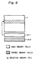
- Fig. 9 which illustrates a state of the normal memory cell array 1 and the redundancy memory cell arrays 2-1 and 2-2 of Fig. 1
- a defective memory cell as indicated by X when a defective memory cell as indicated by X is found in the normal memory cell array 1, rows of memory cells of the normal memory cell array 1 including the defective memory cell are replaced by the redundancy memory cell array 2-1.
- the normal memory cell array 1 except for a shaded portion thereof and the redundancy memory cell array 2-1 are used, while the shaded portion of the normal memory cell array 1 and the redundancy memory cell array 2-2 are unused.
- FIG. 10 is a routine carried out by the sequence control/power supply circuit 13. Also, assume that the sequence control/power supply circuit 13 recognizes the contents of the fuse-type PROMs 1102 and 1103.
- a write operation is performed upon the used memory cells as shown in Fig. 9.
- the sequence control/power supply circuit 13 closes the switches 1104 and 1106, and does not generate the redundancy selection signals RSO' and RS1'.
- the sequence control/power supply circuit 13 generates the program signal PG to activate the write circuit 8 for data "0".
- an address is sequentially incremented and transmitted to the predecoder portion 11.
- the threshold voltages of the used cells are made high.
- a write operation is also performed upon the unused memory cells as shown in Fig. 9.
- the sequence control/power supply circuit 13 opens the switch 1104 and closes the switch 1106.
- the sequence control/power supply circuit 13 generates the program signal PG to activate the write circuit 8 for data "0".
- the address stored in the fuse-type PROM 1102 is generated and transmitted to the predecoder portion 11.
- data "0" is written into the row of the normal memory cell array 1 corresponding to the address stored in the fuse-type PROM 1102.
- the redundancy selection signal RS1' is generated and transmitted to the predecoder portion 11.
- data "0" is written into the redundancy memory cell array 2-2 as indicated by Y1 in Fig. 11A, the threshold voltages of the unused memory cells are also made high.
- a flash erase operation is performed upon the used memory cells and the unused memory cells. That is, the sequence control/voltage supply circuit 13 generates the erase signal ER for a predetermined short time period and transmits it to the erase circuit 5. Therefore, the high power supply voltage V PP is applied to the sources of all the memory cells, while all the word lines WL0, WL1, ⁇ , WLm and the redundancy word lines RWL0, RWL1, ⁇ , RWL7, RWL8, ⁇ , RWL15 are grounded. As a result, all the used memory cells as well as all the unused memory cells are erased. Thus, the threshold voltages of the used memory cells are made low as indicated by X2 in Fig. 11A, and also, the threshold voltages of the unused memory cells are made low as indicated by Y2 in Fig. 11A.
- a verifying operation is performed upon the used memory cells, to determine whether or not the threshold voltages of the used memory cells are lower than an upper limit value VU which is slightly lower than a read voltage at the word lines WL0, WL1, ⁇ WLm, and the redundancy word lines RWL0, RWL1, ⁇ , RWL15.
- the upper limit value VU is 3.0V to 3.5V. That is, the sequence control/power supply circuit 13 closes the switches 1104 and 1106, and does not generate the redundancy selection signals RS0' and RS1' and the program signal PG. Also, the sequence control/power supply circuit 13 sets VU in the voltage V PX . Then, an address is sequentially incremented and transmitted to the predecoder portion 11, so as to determine whether or not the threshold voltages of the used memory cells are lower than the upper limit value VU in accordance with the output of the sense amplifier 10.
- step 1004 when at least one of the threshold voltages of the used memory cells is not lower than the upper limit value VU, the control returns to step 1003, thus repeating the operations at steps 1003 and 1004.
- step 1004 when all the threshold voltages of the used memory cells are lower than the upper limit value VU, the control proceeds to step 1005.
- a verifying operation is performed upon all the used memory cells, to determine whether or not the threshold voltages of the used memory cells are higher than a lower limit value VL which is slightly higher than 0V, for example, 0.3V. That is, at step 1005, it is determined whether or not the used memory cells are not of a depletion type.
- the sequence control/power supply circuit 13 closes the switches 1104 and 1106, and does not generate the redundancy selection signals RS0' and RS1'. Also, the sequence control power supply circuit 13 sets VL in the voltage V SX , while the mode signal MD is made high to turn OFF the transistors 313, 323, ⁇ , 413 and 423. Then, an address is sequentially generated and transmitted to the predecoder portion 11, so as to determine whether or not the threshold voltages of the used memory cells are higher the lower limit value VL in accordance with the output of the sense amplifier 10.
- step 1005 when at least one of the used memory cells is not higher than the lower limit value VL, the control proceeds to step 1008 which determines that the device is failed. Otherwise, the control proceeds to step 1006.
- a verifying operation is performed upon all the unused memory cells, to determine whether or not the threshold voltages of the unused memory cells are higher than the lower limit value VL. That is, at step 1006, it is determined whether or not the unused memory cells are not of a depletion type.
- the sequence control/power supply circuit 13 closes the switch 1104 and and opens the switch 1106. Also, the sequence control power supply circuit 13 sets VL in the voltage V SX , while the mode signal MD is made high to turn OFF the transistors 313, 323, ⁇ , 413 and 423.
- the address stored in the fuse-type PROM 1102 is generated to the predecoder portion 11, so as to determine whether or not the unused memory cells of the normal memory cell array 1 are higher than the lower limit value VL in accordance with the output of the sense amplifier 10.
- the redundancy selection signal RS1' is generated and transmitted to the predecoder portion 11, so as to determine whether or not the threshold voltages of the unused memory cells of the redundancy memory cell array 2-2 are higher the lower limit value VL in accordance with the output of the sense amplifier 10.
- step 1006 when at least one of the unused memory cells is not higher than the lower limit value VL, the control proceeds to step 1008 which determines that the device is failed. Otherwise, the control proceeds to step 1007 which determines that the device is passed.
- step 1002 of Fig. 10 is deleted, and step 1201 is provided instead of step 1006 of Fig. 10.
- a write operation is performed upon the used memory cells as shown in Fig. 9.
- the sequence control/power supply circuit 13 closes the switches 1104 and 1106, and does not generate the redundancy selection signals RSO' and RS1'.
- the sequence control/power supply circuit 13 generates the program signal PG to activate the write circuit 8 for data "0".
- an address is sequentially incremented and transmitted to the predecoder portion 11.
- the threshold voltages of the used cells are made high.
- step 1003 a flash erase operation is performed upon the used memory cells and the unused memory cells. That is, the sequence control/voltage supply circuit 13 generates the erase signal ER for a predetermined short time period and transmits it to the erase circuit 5. Therefore, the high power supply voltage V PP is applied to the sources of all the memory cells, while all the word lines WL0, WL1, ⁇ , WLm and the redundancy word lines RWL0, RWL1, ⁇ , RWL7, RWL8, ⁇ , RWL15 are grounded. As a result, all the used memory cells as well as all the unused memory cells are erased. Thus, the threshold voltages of the used memory cells are made low as indicated by X2 in Fig.
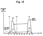
- the threshold voltages of the unused memory cells are made low as indicated by Y1' in Fig. 13.
- Fig. 13 assume that the used memory cells after the flash erase operation are not of a depletion type as indicated by X2 in Fig. 13, and some of the unused memory cells after the flash erase operation are of a depletion type as indicated by Y1' in Fig. 13.
- a verifying operation is performed upon the used memory cells, to determine whether or not the threshold voltages of the used memory cells are lower than the upper limit value VU. That is, the sequence control/power supply circuit 13 closes the switches 1104 and 1106, and does not generate the redundancy selection signals RS0' and RS1' and the program signal PG. Also, the sequence control/power supply circuit 13 sets VU in the voltage V PX . Then, an address is sequentially incremented and transmitted to the predecoder portion 11, so as to determine whether or not the threshold voltages of the used memory cells are lower than the upper limit value VU in accordance with the output of the sense amplifier 10.
- step 1004 when at least one of the threshold voltages of the used memory cells is not lower than the upper limit value VU, the control returns to step 1003, thus repeating the operations at steps 1003 and 1004.
- step 1004 when all the threshold voltages of the used memory cells are lower than the upper limit value VU, the control proceeds to step 1005.
- a verifying operation is performed upon all the used memory cells, to determine whether or not the threshold voltages of the used memory cells are higher than the lower limit value VL. That is, at step 1005, it is determined whether or not the used memory cells are not of a depletion type.
- the sequence control/power supply circuit 13 closes the switches 1104 and 1106, and does not generate the redundancy selection signals RS0' and RS1'. Also, the sequence control power supply circuit 13 sets VL in the voltage V sx , while the mode signal MD is made high to turn OFF the transistors 313, 323, ⁇ , 413 and 423. Then, an address is sequentially generated and transmitted to the predecoder portion 11, so as to determine whether or not the threshold voltages of the used memory cells are higher the lower limit value VL in accordance with the output of the sense amplifier 10.
- step 1005 when at least one of the used memory cells is not higher than the lower limit value VL, the control proceeds to step 1008 which determines that the device is failed. Otherwise, the control proceeds to step 1201.
- a write operation is also performed upon the unused memory cells as shown in Fig. 9.
- the sequence control/power supply circuit 13 opens the switch 1104 and closes the switch 1106.
- the sequence control/power supply circuit 13 generates the program signal PG to activate the write circuit 8 for data "0".
- the address stored in the fuse-type PROM 1102 is generated and transmitted to the predecoder portion 11.
- data "0" is written into the row of the normal memory cell array 1 corresponding to the address stored in the fuse-type PROM 1102.
- the redundancy selection signal RS1' is generated and transmitted to the predecoder portion 11.
- step 1007 determines that the device is passed.
- the over-erased unused memory cells can be corrected by the write operation at step 1201.
- the device which is determined to be failed in the prior art method as shown in Fig. 11D can be determined to be passed.
- step 1401 is added to the routine of Fig. 12. That is, at step 1401, a verifying operation is performed upon all the used memory cells, to determine whether or not the threshold voltages of the used memory cells are higher than a lower limit value VL which is slightly higher than 0V, for example, 0.3V. That is, at step 1401, it is determined whether or not the used memory cells are not of a depletion type. In this case, the sequence control/power supply circuit 13 closes the switches 1104 and 1106, and does not generate the redundancy selection signals RS0' and RS1'.
- the sequence control power supply circuit 13 sets VL in the voltage V SX , while the mode signal MD is made high to turn OFF the transistors 313, 323, ⁇ , 413 and 423. Then, an address is sequentially generated and transmitted to the predecoder portion 11, so as to determine whether or not the threshold voltages of the used memory cells are higher than the lower limit value VL in accordance with the output of the sense amplifier 10.
- step 1401 when at least one of the used memory cells is not higher than the lower limit value VL, the control returns to step 1201. Thus, the write operation at step 1201 is repeated until the threshold voltages of all the unsed memory cells are not of a depletion type. Then, the control proceeds to step 1007 which determines that the device is passed.
- the over-erased unused memory cells can be completely corrected.
- step 1002 is added to the routine of Fig. 12. That is, before the flash erase operation, a write operation is also performed upon the unssed memory cells. As a result, the threshold voltages of the unused memory cells are made high as indicated by Y0' in Fig. 16. This enhances the threshold voltages of the unused memory cells after the write operation at step 1201 is performed. Therefore, the threshold voltages of the unused memory cells are surely made higher as indicated by Y2' in Fig. 16.
- Fig. 17 which illustrates a fourth embodiment of the present invention
- the second embodiment is combined with the third embodiment, i.e., step 1002 is added to the routine of Fig. 14. That is, before the flash erase operation, a write operation is also performed upon the unused memory cells. As a result, the threshold voltages of the unused memory cells are made high. This reduces the number of operations at steps 1201 and 1401, thus reducing the entire time.
- the generation of defective memory cells is often due to a short-circuit between two adjacent word lines. Therefore, even when a write operation is performed upon the memory cells connected to one of the short-circuited word lines, the power supply voltage V PP applied to this one of the short-circuited word lines is reduced by the other of the short-circuited word lines, so that it is impossible to carry out this write operation.
- the two adjacent word lines are simultaneously selected.
- the predecoder 1101 of Fig. 11 can be constructed as illustrated in Fig. 18.
- AND circuits G1-0, G1-1, ⁇ , G1-6 and G1-7 for receiving row address signals A 0 , A 1 and A 2 and their inverted signals are combined with NOR circuits G2-0, G2-1, ⁇ , G2-6, G2-7, respectively, to form NAND circuits.
- AND circuits G3-0, G3-1, ⁇ , G3-6, G3-7 for receiving control signals O and E are combined with the NOR circuits G2-0, G2-1, ⁇ G2-6, G2-7, respectively.
- reference numerals I 0 , I 1 , ⁇ , I 6 and I 7 designate inverters.
- the power supply voltage V PP is applied to one or more of the word lines (i.e., the control gates), and the sources or drains are grounded.
- the write operation can be carried out by the hot electron injection effect.
- the drain voltage may be reduced. In order to avoid this, the drain voltage can be made higher.
- the manufacturing yield of the device can be enhanced.
Abstract
Description
- The present invention relates to a nonvolatile semiconductor memory device, and more particulary, to a method for erasing a nonvolatile memory device incorporating redundancy memory cells.
- In a nonvolatile semiconductor memory device, a write operation can be carried out after the device is mounted on a printed circuit board. One typical example of such a device is a flash memory which has an advantage in that data storage is possible without a backup battery and which is highly integrated. Generally, a memory cell of the flash memory is comprised of a semiconductor substrate having an N+-type source region, an N+-type drain region connected to a bit line, a floating gate over a channel region of the substrate, and a control gate over the floating gate. The control gate is connected to a word line.
- In a flash erase mode, when a positive high voltage is applied to the source region and the control gate is grounded, electrons stored in the floating gate are expelled therefrom. In this case, since the amount of electrons stored in the floating gate immediately before the erase mode affects the threshold voltage of the cell after the erase mode, the threshold voltage is greatly fluctuated. At worst, the threshold voltage of the cell is mode negative by an over-erase phenomenon, i.e., the cell becomes a depletion-type transistor.
- When writing the depletion-type cell, a large leakage current flows between the drain region and the source region to reduce the potential at the drain region, so that it is impossible to carry out a write operation. Also, since a leakage current flows through the depletion-type cell which is non-selected, the other cells connected to the same bit line of the depletion-type cell are deemed to be in an ON state.
- In order to avoid the above-mentioned over-erase phenomenon, a write operation before the flash erase operation is performed upon all the memory cells, to converge the threshold voltages.
- On the other hand, in recent years, even in the nonvolatile memory device, redundancy memory cells are introduced thereinto. That is, if a defective memory cell is found in normal memory cells, the defective memory cell is replaced by its corresponding redundancy memory cell. Thus, the problem of the defective memory cell is alleviated.
- In a prior art method for erasing a nonvolatile semiconductor device incorporating redundancy memory cells, a write operation immediately before a flash erase operation is performed upon the redundancy memory cells as well as the normal memory cells, thus avoiding an over-erase operation for the unused memory cells (see: JP-A-4-159695). This will be explained later in detail.
- In the above-described prior art method, however, although the unused memory cells are actually unused, if at least one of the unused memory cells is over-erased, i.e., of a depletion type, the device is automatically determined to be failed, thus reducing the manufacturing yield of the device.
- In addition, it has been reported that an erratic erase phenomenon may occur in a nonvolatile memory device. That is, an accidental and temporary over-erase phenomenon by traps of holes occurs, and this phenomenon is dissolved by the next write operation. Therefore, it is hard to find the erratic erase phenomenon. Thus in view of the erratic erase phenomenon, the unused memory cells as well as the used memory cells may be over-erased.
- It is an object of the present invention to avoid an over-erase phenomenon for the unused memory cells of a nonvolatile semiconductor memory device incorporating redundancy memory cells, thus enhancing the manufacturing yield of the device.
- According to the present invention, in a nonvolatile memory device, a write operation is performed upon used memory cells. Then, an erase operation is performed upon the used memory cells as well as unused memory cells. Finally, a write operation is performed upon only the unused memory cells. Thus, the threshold voltages of the unused memory cells are ride higher, and accordingly, the depletion phenomenon hardly occurs in the unused memory cells.
- The present invention will be more clearly understood from the description as set forth below, as compared with the prior art, with reference to the accompanying drawings, wherein:
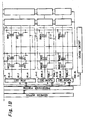
- Figs. 1A and 1B are block circuit diagrams illustrating a prior art semiconductor memory device incorporating redundancy memory cells;
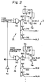
- Fig. 2 is a detailed circuit diagram of the row decoder of Fig. 1;
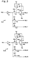
- Fig. 3 is a detailed circuit diagram of the redundancy row decoders of Fig. 1;
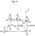
- Fig. 4 is a detailed circuit diagram of the erase circuit of Fig. 1;
- Fig. 5 is a detailed circuit diagram of the column decoder of Fig. 1;
- Fig. 6 is a detailed circuit diagram of the write circuit of Fig. 1;
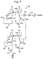
- Fig. 7 is a detailed circuit diagram of the sense amplifier of Fig. 1;
- Fig. 8 is a detailed circuit diagram of the predecoder portion of Fig. 1;
- Fig. 9 is a diagram for explaining used memory cells and unused memory cells of Fig. 1;
- Fig. 10 a flowchart for showing a prior art method for writing, erasing and verifying a nonvolatile memory device;
- Figs. 11A, 11B, 11C and 11D are graphs showing threshold voltage characteristics of memory cells obtained by the routine of Fig. 10;
- Fig. 12 is a flowchart for explaining a first embodiment of the method for writing, earasing and verifying a nonvolatile semiconductor memory device according to the present invention;
- Fig. 13 is a graph showing threshold voltage characteristics of memory cells obtained by the routine of Fig. 12;
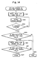
- Fig. 14 is a flowchart for explaining a second embodiment of the method for writing, earasing and verifying a nonvolatile semiconductor memory device according to the present invention;
- Fig. 15 is a flowchart for explaining a third embodiment of the method for writing, earasing and verifying a nonvolatile semiconductor memory device according to the present invention;
- Fig. 16 is a graphs showing threshold voltage characteristics of memory cells obtained by the routine of Fig. 15;
- Fig. 17 is a flowchart for explaining a fourth embodiment of the method for writing, earasing and verifying a nonvolatile semiconductor memory device according to the present invention;
- Fig. 18 is a circuit diagram of a predecoder according to the present invention.
- Before the description of the preferred embodiments, a prior art semiconductor memory device incorporating redundancy memory cells and a prior art method for erasing the device will be explained with reference to Figs. 1A, 1B, 2 through 10, 11A, 11B, 11C and 11D.
- In Figs. 1A and 1B, which illustrate a prior art semiconductor memory device, a plurality of word lines WL0, WL1, ···, WLm, a plurality of redundancy word lines RWL0, RWL1, ···, RWL7, RWL8, RWL9, ···, RWL15, and bit lines BL0, BL1, ···, BLn are provided.
Reference numeral 1 designates a normal memory cell array formed by normal memory cells M00, M01, ···, M0n, M10, M11, ··· each of which has a source, a drain connected to one of the bit lines BL0, BL1, ···, BLn, a floating gate, and a control gate connected to one of the word lines WL1, WL2, ···, WLm. - A redundancy memory cell array 2-1 is formed by redundancy memory cells RM00, RM01, ···, RM0n, ···, each of which has a source, a drain connected to one of the bit lines BL0, BL1, ···, BLn, a floating gate and a control gate connected to one of the redundancy word lines RWL0, RWL1, ···, RWL7. Similarly, a redundancy memory cell array 2-2 is formed by redundancy memory cells RM80, RM81, ···, RM8n, ···, each of which has a source, a drain connected to one of the bit lines BL0, BL1, ···, BLn, a floating gate and a control gate connected to one of the redundancy word lines RWL8, RWL9, ···, RWL15.
- A
row decoder 3 selects one of the word lines WL0, WL1, ···, WLm. Also, a redundancy row decoder 4-1 selects one of the redundancy word lines RWL0, RWL1,···, RWL7, and a redundancy row decoder 4-2 selects one of the redundancy word lines RWL8. - An erase
circuit 5 is connected to all the sources of the normal memory cells M00, M01, ···, M0n, ··· , and the redundacy memory cells RM00, RM01,···, RM0n, ···. As a result, during an erase mode, the voltages at the sources are caused to be high (= Vpp). On the contrary, during a write/read mode, the sources are grounded. - A
column selection circuit 6 is comprised of column selection transistors Qc0, Qc1, ···, Qcn each between one of the bit lines BL0, BL1,···, BLn and a digit line DL0. One of the column selection transistors Qc0, Qc1, ···, Qcn is selected and turned ON by acolumn decoder 7. - A
write circuit 8 receives an input data signal from an imput/output buffer 9 and transmits it to the digit line DLO. Also, asense circuit 10 senses data at the digit line DLO and transmits it to the input/output buffer 9. - The
row decoder 3, the redundancy row decoders 4-1 and 4-2, and thecolumn decoder 7 are controlled by receiving address signals from apredecoder portion 11 which also receives external address signals from anaddress buffer 12 and internal address signals from a sequence control/voltage supply circuit 13. - The sequence control/
voltage supply circuit 13 receives control signals from an input/output buffer 14 to control the entire device. Also, the sequence control/voltage supply circuit 13 supplies power supply voltages such as VPX and VPY to the elements of the device. - Note that the normal
memory cell array 1, the redundancy memory cell arrays 2-1 and 2-2, thecolumn switching circuit 6, thewrite circuit 8, the input/output buffer 9 and thesense amplifier 10 form one block; other blocks such as seven blocks the same as this block are also provided and are connected to the erasecircuit 5. - Each element of the device of Fig. 1 is explained next with reference to Figs. 2 to 8.
- In Fig. 2, which is a detailed circuit diagram of the
row decoder 3 of Fig. 1,circuits circuit 31 is comprised of aNAND circuit 311 for receiving address signals from thepredecoder portion 11, eighttransfer gate transistors 312, P-channel MOS transistors channel MOS transistor 315. In this case, thetransistors NAND circuit 311 receives an inverted signal of a redundancy selection signal RS. Therefore, when the redundancy selection signal RS is high (active), i.e., the redundancy memory cell array 4-1 or 4-2 is selected, the NAND circuit 311 (321) is disabled. Contrary to this, when the redundancy selection signal RS is low (inactive), i.e., the redundancy memory cell arrays 4-1, and 4-2 are not selected, the NAND circuit 311 (321) is enabled. That is, the output of one of theNAND circuits voltage supply circuit 13 is high, thetransistor 313 is turned OFF and thetransistor 314 is turned ON, so that the voltage at the word line WLO is VPX. Note that VPX is VPP such as 12V during a write mode, VPX is VCC such as 5V during a read mode, and VPX is OV during an erase mode. - Further, during a verifying mode for a lower limit value VL of threshold voltage, the mode signal MD is made low. As a result, the
transistors transistors - In Fig. 3, which is a detailed circuit diagram of the redundancy row decoders 4-1 and 4-2, of Fig. 1, the redundancy row decoders 4-1 and 4-2, which have the same configuration, are provided for every eight redundancy word lines such as RWL0, RWL1, ···, RWL7. For example, the redundancy row decoder 4-1 is comprised of an
inverter 411 for a redundancy selection signal RS0 from thepredecoder portion 11, eighttransfer gate transistors 412, P-channel MOS transistors channel MOS transistor 415. In this case, thetransistors inverter 411 is high so that the redundancy memory cell array 4-1 is disabled. Contrary to this, when the redundancy selection signal RS0 is high (active), the output of theinverter 411 is low. Also, one of the predecode signals BX0, BX1, ···, BX7 is made high. For example, if the predecode signal BX0 is high, and the mode signal MD is high, thetransistor 413 is turned OFF and thetransistor 414 is turned ON, so that the voltage at the redundancy word line RWLO is VPX. - Further, during a verifying mode for a lower limit value VL of threshold voltage, the mode signal MD is made low. As a result, the
transistor 413 is turned ON, and accordingly, thetransistor 415 is turned ON. Therefore, a voltage Vsx corresponding to the lower limit value VL is applied to the redundancy word lines RWL0, RWL1, ···. - In Fig. 4, which is a detailed circuit diagram of the erase
circuit 5 of Fig. 1, an erase signal ER is supplied from the sequence control/power supply circuit 13 viainverters channel MOS transistors channel MOS transistors channel MOS transistor 507 and an N-channel MOS transistor 508 are connected in series and are powered by the power supply voltage VPP. The gate of the P-channel MOS transistor 507 is controlled by the output voltage of the flip-flop, while the gate of the N-channel MOS transistor 508 is controlled by an inverted signal of the erase signal ER. During an erase mode (ER = "1"), the output voltage of theinverter 501 is low (= OV), so that thetransistor 508 is turned OFF, and the output voltage of the flip-flop is also low, so that thetransistor 507 is turned ON. As a result, the voltages of the sources are VPP. Contrary to this, during a non-erase mode (ER = "0"), the output voltage of theinverter 501 is high (= VCC), so that thetransistor 508 is turned ON, and the output voltage of the flip-flop is high (= VPP), so that thetransistor 507 is turned OFF. As a result, the voltages of the sources are 0V. - In Fig. 5, which is a detailed circuit diagram of the
column decoder 7 of Fig. 1,circuits circuit 31 is comprised of aNAND circuit 711 for receiving address signals from thepredecoder portion 11, atransitor 712, P-channel MOS transistors channel MOS transistor 715. In this case, thetransistors NAND circuit 711 is low (= 0V), is thetransistor 714 turned ON so that the voltage at the gate of the column selection transistor QC0 is VPY. In this case, thetransistor 713 is turned OFF. Otherwise, when output voltage of theNAND circuit 711 is high, thetransistor 715 is turned ON so that the voltage at the gate of the column selection transistor Q C0 is 0V. In this case, thetransistor 713 is turned ON. - In Fig. 6, which is a detailed circuit diagram of the
write circuit 8 of Fig. 1, thewrite circuit 8 includes aNAND circuit 801 for receiving input data DI via aninverter 802 and a program signal PG from the sequence control/power supply circuit 13. Also, thewrite circuit 8 includes atransfer gate transistor 803, P-channel MOS transistors channel MOS transistor 806. In this case, thetransistors channel MOS transistor 807. In a write mode (PG ="1"), theNAND circuit 801 passes the input data DI therethrough, so that the output of the CMOS inverter is high (= VPG ) or low (= OV) in accordance with the input data DI. Thus, the voltage at the digit line DLO is pulled up to VPP. Conversely, in a read mode (PG ="0"), theNAND circuit 801 is disabled, thus prohibiting the transition of the input data DI therethrough. - In Fig. 7, which is a detailed circuit diagram of the
sense amplifier 10 of Fig. 1, thesense amplifier 10 includes a referencevoltage generating circuit 101 and acomparator 102. The referencevoltage generating circuit 101 is comprised of a variable constantcurrent source 1011, N-channel MOS transistors inverter 1016, and P-channel MOS transistors voltage generating circuit 101, a current determined by thecurrent source 1011 flows through a path formed by theelements elements - The
comparator 102 is comprised of N-channel MOS transistors transistors inverter 1024 corresponding to theinverter 1016, and P-channel MOS transistors transistors transistors inverter 103. Conversely, if the voltage at the digit line DLO is high, a current hardly flows through thetransistors inverter 103. Thus, the output of theinverter 103 is supplied via aninverter 104 to the input/output buffer 9. Note that the sizes of thetransistors - In Fig. 8, which is a partly-detailed circuit diagram of the
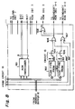
predecoder portion 11 of Fig. 1, arow predecoder 1101 is provided for receiving three lower bits of a row address to generate the predecode signals BX0, BX1, ···, BX7 and transmit them to therow decoder 3 and the redundancy raw decoders 4-1 and 4-2. - Also, fuse-type programmable read-only memories (PROMs) 1102 and 1103 are provided for storing row addresses defined by the upper bits of the row address except for the above-mentioned three lower hits. That is, when one or more memory cells are determined to be defective in the normal
memory cell array 1, row addresses indicating such defective memory cells are written into the fuse-type PROMs type PROMs type PROM memory cell array 1 including the defective memory cell with the redundancy memory cell array 2-1 or 2-2. Thus, the defective memory cells are alleviated. - The redundancy selection signal RS0 generated from the fuse-
type PROM 1102 is transmitted via aswitch 1104 and anOR circuit 1105 to the redundancy row decoder 4-1. Similarly, the redundancy selection signal RS1 generated from the fuse-type PROM 1103 is transmitted via aswitch 1106 and anOR circuit 1107 to the redundancy row decoder 4-2. Also, the redundancy selection signals RS0 and RS1 are transmitted via anOR circuit 1108 as the redundancy selection signal RS to therow decoder 3. That is, when at least one of the redundancy memory cell arrays 2-1 and 2-2 is selected, therow decoder 3 is disabled. - The
switches power supply circuit 13. For example, even if the redundancy selection signal RSO is generated from the fuse-type PROM 1102, the sequence control/power supply voltage 13 makes theswitch 1104 open, so that the row of the memory cells including a defective memory cell can be selected in the normalmemory cell array 1. - On the other hand, redundancy selection signals RSO' and RS1' are supplied from the sequence control/
power supply circuit 13 via theOR circuits type PROM 1102, the sequence control/power supply circuit 13 generates the redundancy selection signal RS0', so that the redundancy memory cell array 2-1 can be selected. - In Fig. 9, which illustrates a state of the normal
memory cell array 1 and the redundancy memory cell arrays 2-1 and 2-2 of Fig. 1, when a defective memory cell as indicated by X is found in the normalmemory cell array 1, rows of memory cells of the normalmemory cell array 1 including the defective memory cell are replaced by the redundancy memory cell array 2-1. In this case, the normalmemory cell array 1 except for a shaded portion thereof and the redundancy memory cell array 2-1 are used, while the shaded portion of the normalmemory cell array 1 and the redundancy memory cell array 2-2 are unused. - A prior art method for writing, erasing and verifying the memory calls of Fig. 1 is explained next with reference to Fig. 10 as well as Figs. 9 and 11A, 11B, 11C and 11D. Note that Fig. 10 is a routine carried out by the sequence control/
power supply circuit 13. Also, assume that the sequence control/power supply circuit 13 recognizes the contents of the fuse-type PROMs - First, at
step 1001, a write operation is performed upon the used memory cells as shown in Fig. 9. In this case, the sequence control/power supply circuit 13 closes theswitches power supply circuit 13 generates the program signal PG to activate thewrite circuit 8 for data "0". Then, an address is sequentially incremented and transmitted to thepredecoder portion 11. As a result, as indicated by X1 in Fig. 11A, the threshold voltages of the used cells are made high. - Next, at
step 1002, a write operation is also performed upon the unused memory cells as shown in Fig. 9. In this case, the sequence control/power supply circuit 13 opens theswitch 1104 and closes theswitch 1106. Also, the sequence control/power supply circuit 13 generates the program signal PG to activate thewrite circuit 8 for data "0". Then, the address stored in the fuse-type PROM 1102 is generated and transmitted to thepredecoder portion 11. As a result, data "0" is written into the row of the normalmemory cell array 1 corresponding to the address stored in the fuse-type PROM 1102. Then, the redundancy selection signal RS1' is generated and transmitted to thepredecoder portion 11. As a result, data "0" is written into the redundancy memory cell array 2-2 as indicated by Y1 in Fig. 11A, the threshold voltages of the unused memory cells are also made high. - Next, at
step 1003, a flash erase operation is performed upon the used memory cells and the unused memory cells. That is, the sequence control/voltage supply circuit 13 generates the erase signal ER for a predetermined short time period and transmits it to the erasecircuit 5. Therefore, the high power supply voltage VPP is applied to the sources of all the memory cells, while all the word lines WL0, WL1, ···, WLm and the redundancy word lines RWL0, RWL1, ···, RWL7, RWL8, ···, RWL15 are grounded. As a result, all the used memory cells as well as all the unused memory cells are erased. Thus, the threshold voltages of the used memory cells are made low as indicated by X2 in Fig. 11A, and also, the threshold voltages of the unused memory cells are made low as indicated by Y2 in Fig. 11A. - Next, at
step 1004, a verifying operation is performed upon the used memory cells, to determine whether or not the threshold voltages of the used memory cells are lower than an upper limit value VU which is slightly lower than a read voltage at the word lines WL0, WL1, ··· WLm, and the redundancy word lines RWL0, RWL1, ··· , RWL15. For example, the upper limit value VU is 3.0V to 3.5V. That is, the sequence control/power supply circuit 13 closes theswitches power supply circuit 13 sets VU in the voltage VPX.
Then, an address is sequentially incremented and transmitted to thepredecoder portion 11, so as to determine whether or not the threshold voltages of the used memory cells are lower than the upper limit value VU in accordance with the output of thesense amplifier 10. - At
step 1004, when at least one of the threshold voltages of the used memory cells is not lower than the upper limit value VU, the control returns to step 1003, thus repeating the operations atsteps - At
step 1004, when all the threshold voltages of the used memory cells are lower than the upper limit value VU, the control proceeds to step 1005. - At
step 1005, a verifying operation is performed upon all the used memory cells, to determine whether or not the threshold voltages of the used memory cells are higher than a lower limit value VL which is slightly higher than 0V, for example, 0.3V. That is, atstep 1005, it is determined whether or not the used memory cells are not of a depletion type. In this case, the sequence control/power supply circuit 13 closes theswitches power supply circuit 13 sets VL in the voltage VSX, while the mode signal MD is made high to turn OFF thetransistors predecoder portion 11, so as to determine whether or not the threshold voltages of the used memory cells are higher the lower limit value VL in accordance with the output of thesense amplifier 10. - At
step 1005, when at least one of the used memory cells is not higher than the lower limit value VL, the control proceeds to step 1008 which determines that the device is failed. Otherwise, the control proceeds to step 1006. - At
step 1006, a verifying operation is performed upon all the unused memory cells, to determine whether or not the threshold voltages of the unused memory cells are higher than the lower limit value VL. That is, atstep 1006, it is determined whether or not the unused memory cells are not of a depletion type. In this case, the sequence control/power supply circuit 13 closes theswitch 1104 and and opens theswitch 1106. Also, the sequence controlpower supply circuit 13 sets VL in the voltage VSX, while the mode signal MD is made high to turn OFF thetransistors type PROM 1102 is generated to thepredecoder portion 11, so as to determine whether or not the unused memory cells of the normalmemory cell array 1 are higher than the lower limit value VL in accordance with the output of thesense amplifier 10. Then, the redundancy selection signal RS1' is generated and transmitted to thepredecoder portion 11, so as to determine whether or not the threshold voltages of the unused memory cells of the redundancy memory cell array 2-2 are higher the lower limit value VL in accordance with the output of thesense amplifier 10. - At
step 1006, when at least one of the unused memory cells is not higher than the lower limit value VL, the control proceeds to step 1008 which determines that the device is failed. Otherwise, the control proceeds to step 1007 which determines that the device is passed. - According to the routine of Fig. 10, when the determinations at
steps steps step 1005 is negative and the determination atstep 1006 is affirmative as shown in Fig. 11C, or when the determination atstep 1005 is affirmative and the determination atstep 1006 is negative as shown in Fig. 11D, the device is determined to be failed. - In Fig. 12, which illustrates a first embodiment of the present invention,
step 1002 of Fig. 10 is deleted, andstep 1201 is provided instead ofstep 1006 of Fig. 10. - First, at
step 1001, a write operation is performed upon the used memory cells as shown in Fig. 9. In this case, the sequence control/power supply circuit 13 closes theswitches power supply circuit 13 generates the program signal PG to activate thewrite circuit 8 for data "0". Then, an address is sequentially incremented and transmitted to thepredecoder portion 11. As a result, as indicated by X1 in Fig. 13, the threshold voltages of the used cells are made high. - Next, at
step 1003, a flash erase operation is performed upon the used memory cells and the unused memory cells. That is, the sequence control/voltage supply circuit 13 generates the erase signal ER for a predetermined short time period and transmits it to the erasecircuit 5. Therefore, the high power supply voltage VPP is applied to the sources of all the memory cells, while all the word lines WL0, WL1, ···, WLm and the redundancy word lines RWL0, RWL1, ···, RWL7, RWL8, ···, RWL15 are grounded. As a result, all the used memory cells as well as all the unused memory cells are erased. Thus, the threshold voltages of the used memory cells are made low as indicated by X2 in Fig. 13, and also, the threshold voltages of the unused memory cells are made low as indicated by Y1' in Fig. 13. In Fig. 13, assume that the used memory cells after the flash erase operation are not of a depletion type as indicated by X2 in Fig. 13, and some of the unused memory cells after the flash erase operation are of a depletion type as indicated by Y1' in Fig. 13. - Next, at
step 1004, a verifying operation is performed upon the used memory cells, to determine whether or not the threshold voltages of the used memory cells are lower than the upper limit value VU. That is, the sequence control/power supply circuit 13 closes theswitches power supply circuit 13 sets VU in the voltage VPX. Then, an address is sequentially incremented and transmitted to thepredecoder portion 11, so as to determine whether or not the threshold voltages of the used memory cells are lower than the upper limit value VU in accordance with the output of thesense amplifier 10. - At
step 1004, when at least one of the threshold voltages of the used memory cells is not lower than the upper limit value VU, the control returns to step 1003, thus repeating the operations atsteps - At
step 1004, when all the threshold voltages of the used memory cells are lower than the upper limit value VU, the control proceeds to step 1005. - At
step 1005, a verifying operation is performed upon all the used memory cells, to determine whether or not the threshold voltages of the used memory cells are higher than the lower limit value VL. That is, atstep 1005, it is determined whether or not the used memory cells are not of a depletion type. In this case, the sequence control/power supply circuit 13 closes theswitches power supply circuit 13 sets VL in the voltage Vsx, while the mode signal MD is made high to turn OFF thetransistors predecoder portion 11, so as to determine whether or not the threshold voltages of the used memory cells are higher the lower limit value VL in accordance with the output of thesense amplifier 10. - At
step 1005, when at least one of the used memory cells is not higher than the lower limit value VL, the control proceeds to step 1008 which determines that the device is failed. Otherwise, the control proceeds to step 1201. - At
step 1201, a write operation is also performed upon the unused memory cells as shown in Fig. 9. In this case, the sequence control/power supply circuit 13 opens theswitch 1104 and closes theswitch 1106. Also, the sequence control/power supply circuit 13 generates the program signal PG to activate thewrite circuit 8 for data "0". Then, the address stored in the fuse-type PROM 1102 is generated and transmitted to thepredecoder portion 11. As a result, data "0" is written into the row of the normalmemory cell array 1 corresponding to the address stored in the fuse-type PROM 1102. Then, the redundancy selection signal RS1' is generated and transmitted to thepredecoder portion 11. As a result, data "0" is written into the redundancy memory cell array 2-2 as indicated by Y2' in Fig. 13, the threshold voltages of the unused memory cells are also made high. Then, the control proceeds to step 1007 which determines that the device is passed. - According to the first embodiment as illustrated in Fig. 12, even when the threshold voltages of the unsed memory cells are over-erased as indicated by Y1' in Fig. 13, the over-erased unused memory cells can be corrected by the write operation at
step 1201. Thus, the device which is determined to be failed in the prior art method as shown in Fig. 11D can be determined to be passed. - In Fig. 14, which illustrates a second embodiment of the present invention,
step 1401 is added to the routine of Fig. 12. That is, atstep 1401, a verifying operation is performed upon all the used memory cells, to determine whether or not the threshold voltages of the used memory cells are higher than a lower limit value VL which is slightly higher than 0V, for example, 0.3V. That is, atstep 1401, it is determined whether or not the used memory cells are not of a depletion type. In this case, the sequence control/power supply circuit 13 closes theswitches power supply circuit 13 sets VL in the voltage VSX, while the mode signal MD is made high to turn OFF thetransistors predecoder portion 11, so as to determine whether or not the threshold voltages of the used memory cells are higher than the lower limit value VL in accordance with the output of thesense amplifier 10. - At
step 1401, when at least one of the used memory cells is not higher than the lower limit value VL, the control returns to step 1201. Thus, the write operation atstep 1201 is repeated until the threshold voltages of all the unsed memory cells are not of a depletion type. Then, the control proceeds to step 1007 which determines that the device is passed. - According to the second embodiment as illustrated in Fig. 14, the over-erased unused memory cells can be completely corrected.
- In Fig. 15, which illustrates a third embodiment of the present invention,
step 1002 is added to the routine of Fig. 12. That is, before the flash erase operation, a write operation is also performed upon the unssed memory cells. As a result, the threshold voltages of the unused memory cells are made high as indicated by Y0' in Fig. 16. This enhances the threshold voltages of the unused memory cells after the write operation atstep 1201 is performed. Therefore, the threshold voltages of the unused memory cells are surely made higher as indicated by Y2' in Fig. 16. - In Fig. 17, which illustrates a fourth embodiment of the present invention, the second embodiment is combined with the third embodiment, i.e.,
step 1002 is added to the routine of Fig. 14. That is, before the flash erase operation, a write operation is also performed upon the unused memory cells. As a result, the threshold voltages of the unused memory cells are made high. This reduces the number of operations atsteps - Actually, the generation of defective memory cells is often due to a short-circuit between two adjacent word lines. Therefore, even when a write operation is performed upon the memory cells connected to one of the short-circuited word lines, the power supply voltage VPP applied to this one of the short-circuited word lines is reduced by the other of the short-circuited word lines, so that it is impossible to carry out this write operation. In order to surely perform a write operation upon the defective memory cells due to the short-circuit of two adjacent word lines, the two adjacent word lines are simultaneously selected. For this purpose, the
predecoder 1101 of Fig. 11 can be constructed as illustrated in Fig. 18. - In Fig. 18, AND circuits G1-0, G1-1, ···, G1-6 and G1-7 for receiving row address signals A0, A1 and A2 and their inverted signals are combined with NOR circuits G2-0, G2-1, ···, G2-6, G2-7, respectively, to form NAND circuits. Also, AND circuits G3-0, G3-1, ···, G3-6, G3-7 for receiving control signals O and E are combined with the NOR circuits G2-0, G2-1, ··· G2-6, G2-7, respectively. Also, reference numerals I0 , I1, ···, I6 and I7 designate inverters. For example, if


- In the above-described write operation, the power supply voltage VPP is applied to one or more of the word lines (i.e., the control gates), and the sources or drains are grounded. As a result, electrons are expelled from the floating gates to the sources or drains ultilizing the Fowler-Nordheim tunnelling. However, the write operation can be carried out by the hot electron injection effect. In this case, when simultaneously accessing two word lines, the drain voltage may be reduced. In order to avoid this, the drain voltage can be made higher.
- As explained hereinbefore, according to the present invention, since the over-erase of the unused memory cells can be compensated for, the manufacturing yield of the device can be enhanced.
Claims (14)
- A method for writing, erasing and writing a nonvolatile semiconductor memory device including used memory cells and unused memory cells, comprising the steps of:performing a first write operation upon said used memory cells;performing an erase operation upon said used memory cells and said unused memory cells, after said first write operation performed; andperforming a second write operation upon said unused memory cells.
- The method as set forth in claim 1, wherein said nonvolatile semiconductor device includes normal memory cells (M00, M01, ···) and redundancy memory cells (RM00, RM01,···)said used memory cells being forming by said normal memory cells and said unused memory cells being formed by said redundancy memory cells, when all said normal memory cells are not defective,a portion of said redundancy memory cells replacing a portion of said normal memory cells so that said used memory cells are formed by said normal memory cells except for said portion of said normal memory cells and said portion of said redundancy memory cells and said unused memory cells are formed by said portion of said normal memory cells and said redunancy memory cells except for said portion of said redundancy memory cells, when said portion of said normal memory cells are defective.
- The method as set forth in claim 1, further comprising the steps of:performing a verifying operation upon said used memory cells and said unused memory cells to verify whether or not threshold voltages of said used memory cells and said unused memory cells are lower than an upper limit value (VU), after said erase operation is performed; andrepeating said erase operation and said verifying operation, when at least one of the threshold voltages is not lower than said upper limit value.
- The method as set forth in claim 1, further comprising the steps of:performing a verifying operation upon said unused memory cells to verify whether or not threshold voltages of said unused memory cells are higher than a lower limit value (VL), after said second write operation is performed; andrepeating said second write operation and said verifying operation, when at least one of the threshold voltages is not higher than said lower limit value.
- The method as set forth in claim 1, wherein said second write operation is performed by simultaneously selecting a plurality of word lines connected to said unnused memory cells.
- The method as set forth in claim 1, wherein said second write operation is performed by using a tunnelling effect.
- The method as set forth in claim 1, wherein said second write operation is performed by hot electron injection effect.
- The method as set forth in claim 1, further comprising a step of performing a third write operation upon said unused memory cells, before said erase operation is performed.
- The method as set forth in claim 8, wherein said third write operation is performed by simultaneously selecting a plurality of word lines connected to said unnused memory cells.
- The method as set forth in claim 8, wherein said third write operation is performed by using a tunnelling effect.
- The method as set forth in claim 8, wherein said third write operation is performed by a hot electron injection effect.
- A nonvolatile memory device comprising:used memory cells; andunused memory cells whose threshold voltages are positive.
- The device as set forth in claim 12, wherein said used memory cells are formed by normal memory cells (M00, M01,···) and said unused memory cells are formed by redundancy memory cells (RM00, RM01, ···), when said normal memory cells are not defective,said used memory cells being formed by said normal memory cells except for a portion of said normal memory cells and a portion of said redundancy memory cells, and said unused memory cells being formed by said portion of said normal memory cells and said redundancy memory cells except for said portion of said redundancy memory cells, when said portion of said normal memory cells are defective so that said portion of said normal memory cells replace said portion of said redundancy memory cells.
- The device as set forth in claim 12, further comprising means for simultaneously selecting a plurality of word lines connected to said memory cells to perform a write operation upon said memory cells through said word lines.
Applications Claiming Priority (3)
| Application Number | Priority Date | Filing Date | Title |
|---|---|---|---|
| JP79850/95 | 1995-03-10 | ||
| JP7985095 | 1995-03-10 | ||
| JP7985095A JP3145894B2 (en) | 1995-03-10 | 1995-03-10 | Electrically writable / erasable nonvolatile semiconductor memory device |
Publications (3)
| Publication Number | Publication Date |
|---|---|
| EP0731470A2 true EP0731470A2 (en) | 1996-09-11 |
| EP0731470A3 EP0731470A3 (en) | 1999-04-14 |
| EP0731470B1 EP0731470B1 (en) | 2003-07-09 |
Family
ID=13701681
Family Applications (1)
| Application Number | Title | Priority Date | Filing Date |
|---|---|---|---|
| EP96103675A Expired - Lifetime EP0731470B1 (en) | 1995-03-10 | 1996-03-08 | Method for erasing nonvolatile semiconductor memory device incorporating redundancy memory cells |
Country Status (4)
| Country | Link |
|---|---|
| US (1) | US5684747A (en) |
| EP (1) | EP0731470B1 (en) |
| JP (1) | JP3145894B2 (en) |
| DE (1) | DE69628963T2 (en) |
Families Citing this family (12)
| Publication number | Priority date | Publication date | Assignee | Title |
|---|---|---|---|---|
| JP3600424B2 (en) * | 1997-02-26 | 2004-12-15 | 株式会社東芝 | Semiconductor storage device |
| JP2005092962A (en) | 2003-09-16 | 2005-04-07 | Renesas Technology Corp | Nonvolatile semiconductor storage device |
| US9330783B1 (en) | 2014-12-17 | 2016-05-03 | Apple Inc. | Identifying word-line-to-substrate and word-line-to-word-line short-circuit events in a memory block |
| US9390809B1 (en) * | 2015-02-10 | 2016-07-12 | Apple Inc. | Data storage in a memory block following WL-WL short |
| US9529663B1 (en) | 2015-12-20 | 2016-12-27 | Apple Inc. | Detection and localization of failures in 3D NAND flash memory |
| US9996417B2 (en) | 2016-04-12 | 2018-06-12 | Apple Inc. | Data recovery in memory having multiple failure modes |
| US10910061B2 (en) * | 2018-03-14 | 2021-02-02 | Silicon Storage Technology, Inc. | Method and apparatus for programming analog neural memory in a deep learning artificial neural network |
| US10762967B2 (en) | 2018-06-28 | 2020-09-01 | Apple Inc. | Recovering from failure in programming a nonvolatile memory |
| US10755787B2 (en) | 2018-06-28 | 2020-08-25 | Apple Inc. | Efficient post programming verification in a nonvolatile memory |
| US10936455B2 (en) | 2019-02-11 | 2021-03-02 | Apple Inc. | Recovery of data failing due to impairment whose severity depends on bit-significance value |
| US10915394B1 (en) | 2019-09-22 | 2021-02-09 | Apple Inc. | Schemes for protecting data in NVM device using small storage footprint |
| US11550657B1 (en) | 2021-09-01 | 2023-01-10 | Apple Inc. | Efficient programming schemes in a nonvolatile memory |
Citations (4)
| Publication number | Priority date | Publication date | Assignee | Title |
|---|---|---|---|---|
| EP0501289A2 (en) * | 1991-02-20 | 1992-09-02 | Sundisk Corporation | Method and structure for programming floating gate memory |
| US5233559A (en) * | 1991-02-11 | 1993-08-03 | Intel Corporation | Row redundancy for flash memories |
| EP0570597A1 (en) * | 1991-12-09 | 1993-11-24 | Fujitsu Limited | Flash memory improved in erasing characteristic, and circuit therefor |
| US5327383A (en) * | 1992-04-21 | 1994-07-05 | Intel Corporation | Method and circuitry for erasing a nonvolatile semiconductor memory incorporating row redundancy |
Family Cites Families (12)
| Publication number | Priority date | Publication date | Assignee | Title |
|---|---|---|---|---|
| JP2638654B2 (en) * | 1990-02-06 | 1997-08-06 | 三菱電機株式会社 | Semiconductor nonvolatile storage device |
| JPH04159696A (en) * | 1990-10-22 | 1992-06-02 | Mitsubishi Electric Corp | Nonvolatile semiconductor memory |
| JPH04214300A (en) * | 1990-12-12 | 1992-08-05 | Mitsubishi Electric Corp | Nonvolatile semiconductor memory device |
| JPH05182480A (en) * | 1991-12-28 | 1993-07-23 | Sony Corp | Programmable read only memory |
| JP2716906B2 (en) * | 1992-03-27 | 1998-02-18 | 株式会社東芝 | Nonvolatile semiconductor memory device |
| US5347489A (en) * | 1992-04-21 | 1994-09-13 | Intel Corporation | Method and circuitry for preconditioning shorted rows in a nonvolatile semiconductor memory incorporating row redundancy |
| JPH0676589A (en) * | 1992-07-06 | 1994-03-18 | Sony Corp | Method for erasing flash type e2prom |
| JPH0628875A (en) * | 1992-07-10 | 1994-02-04 | Sony Corp | Method for erasing frash type eeprom |
| US5357475A (en) * | 1992-10-30 | 1994-10-18 | Intel Corporation | Method for detaching sectors in a flash EEPROM memory array |
| JPH06150674A (en) * | 1992-11-09 | 1994-05-31 | Seiko Epson Corp | Nonvolatile semiconductor device |
| JPH06275095A (en) * | 1993-03-18 | 1994-09-30 | Fujitsu Ltd | Semiconductor memory and writing method for redundant address |
| US5559742A (en) * | 1995-02-23 | 1996-09-24 | Micron Technology, Inc. | Flash memory having transistor redundancy |
-
1995
- 1995-03-10 JP JP7985095A patent/JP3145894B2/en not_active Expired - Fee Related
-
1996
- 1996-03-08 DE DE69628963T patent/DE69628963T2/en not_active Expired - Fee Related
- 1996-03-08 EP EP96103675A patent/EP0731470B1/en not_active Expired - Lifetime
- 1996-03-11 US US08/613,911 patent/US5684747A/en not_active Expired - Lifetime
Patent Citations (4)
| Publication number | Priority date | Publication date | Assignee | Title |
|---|---|---|---|---|
| US5233559A (en) * | 1991-02-11 | 1993-08-03 | Intel Corporation | Row redundancy for flash memories |
| EP0501289A2 (en) * | 1991-02-20 | 1992-09-02 | Sundisk Corporation | Method and structure for programming floating gate memory |
| EP0570597A1 (en) * | 1991-12-09 | 1993-11-24 | Fujitsu Limited | Flash memory improved in erasing characteristic, and circuit therefor |
| US5327383A (en) * | 1992-04-21 | 1994-07-05 | Intel Corporation | Method and circuitry for erasing a nonvolatile semiconductor memory incorporating row redundancy |
Also Published As
| Publication number | Publication date |
|---|---|
| JP3145894B2 (en) | 2001-03-12 |
| DE69628963D1 (en) | 2003-08-14 |
| EP0731470A3 (en) | 1999-04-14 |
| US5684747A (en) | 1997-11-04 |
| DE69628963T2 (en) | 2004-05-27 |
| JPH08249900A (en) | 1996-09-27 |
| EP0731470B1 (en) | 2003-07-09 |
Similar Documents
| Publication | Publication Date | Title |
|---|---|---|
| KR960007638B1 (en) | Electrically and flash erasable non volatile semiconductor memory device | |
| US6525960B2 (en) | Nonvolatile semiconductor memory device including correction of erratic memory cell data | |
| JP3661164B2 (en) | Program method for nonvolatile semiconductor memory | |
| JP3836643B2 (en) | Nonvolatile integrated circuit memory device and driving method thereof | |
| US5541879A (en) | Nonvolatile semiconductor memory having program verifying circuit | |
| JP3167919B2 (en) | Nonvolatile semiconductor memory having NAND structure and method of programming the same | |
| JP3898349B2 (en) | Semiconductor memory device | |
| USRE44350E1 (en) | Nonvolatile semiconductor memory including multi-threshold voltage memory cells including voltage ranges indicating either an erase state or a two or more program state | |
| US7002844B2 (en) | Method of repairing a failed wordline | |
| JPH06215591A (en) | Nonvolatile semiconductor storage | |
| JP3392165B2 (en) | Semiconductor storage device | |
| US5400287A (en) | Method for erasing and verifying nonvolatile semiconductor memory device | |
| US5684747A (en) | Method for erasing nonvolatile semiconductor memory device incorporating redundancy memory cells | |
| JP3615009B2 (en) | Semiconductor memory device | |
| JP2001143489A (en) | Nonvolatile semiconductor memory in which read-out time is shortened | |
| US5668759A (en) | Method for erasing and verifying nonvolatile semiconductor memory | |
| US6373750B1 (en) | Non-volatile memory which performs erasure in a short time | |
| KR19980018548A (en) | Nonvolatile memory | |
| KR0172364B1 (en) | Elimination detecting method using reference cell of non-volatile semiconductor memory | |
| JP3360855B2 (en) | Batch erase nonvolatile semiconductor memory device and test method therefor | |
| JPH05210993A (en) | Nonvolatile semiconductor memory | |
| JPH0917189A (en) | Non-volatile semiconductor memory | |
| JP3190082B2 (en) | Semiconductor storage device | |
| JPH06103798A (en) | Semiconductor memory | |
| JPH04214300A (en) | Nonvolatile semiconductor memory device |
Legal Events
| Date | Code | Title | Description |
|---|---|---|---|
| PUAI | Public reference made under article 153(3) epc to a published international application that has entered the european phase |
Free format text: ORIGINAL CODE: 0009012 |
|
| AK | Designated contracting states |
Kind code of ref document: A2 Designated state(s): DE FR GB IT NL |
|
| PUAL | Search report despatched |
Free format text: ORIGINAL CODE: 0009013 |
|
| AK | Designated contracting states |
Kind code of ref document: A3 Designated state(s): DE FR GB IT NL |
|
| 17P | Request for examination filed |
Effective date: 19990721 |
|
| 17Q | First examination report despatched |
Effective date: 20001228 |
|
| GRAG | Despatch of communication of intention to grant |
Free format text: ORIGINAL CODE: EPIDOS AGRA |
|
| GRAG | Despatch of communication of intention to grant |
Free format text: ORIGINAL CODE: EPIDOS AGRA |
|
| GRAH | Despatch of communication of intention to grant a patent |
Free format text: ORIGINAL CODE: EPIDOS IGRA |
|
| GRAH | Despatch of communication of intention to grant a patent |
Free format text: ORIGINAL CODE: EPIDOS IGRA |
|
| RAP1 | Party data changed (applicant data changed or rights of an application transferred) |
Owner name: NEC ELECTRONICS CORPORATION |
|
| GRAA | (expected) grant |
Free format text: ORIGINAL CODE: 0009210 |
|
| AK | Designated contracting states |
Designated state(s): DE FR GB IT NL |
|
| PG25 | Lapsed in a contracting state [announced via postgrant information from national office to epo] |
Ref country code: NL Free format text: LAPSE BECAUSE OF FAILURE TO SUBMIT A TRANSLATION OF THE DESCRIPTION OR TO PAY THE FEE WITHIN THE PRESCRIBED TIME-LIMIT Effective date: 20030709 Ref country code: FR Free format text: LAPSE BECAUSE OF NON-PAYMENT OF DUE FEES Effective date: 20030709 |
|
| REG | Reference to a national code |
Ref country code: GB Ref legal event code: FG4D |
|
| REF | Corresponds to: |
Ref document number: 69628963 Country of ref document: DE Date of ref document: 20030814 Kind code of ref document: P |
|
| NLV1 | Nl: lapsed or annulled due to failure to fulfill the requirements of art. 29p and 29m of the patents act | ||
| PG25 | Lapsed in a contracting state [announced via postgrant information from national office to epo] |
Ref country code: GB Free format text: LAPSE BECAUSE OF NON-PAYMENT OF DUE FEES Effective date: 20040308 |
|
| PLBE | No opposition filed within time limit |
Free format text: ORIGINAL CODE: 0009261 |
|
| STAA | Information on the status of an ep patent application or granted ep patent |
Free format text: STATUS: NO OPPOSITION FILED WITHIN TIME LIMIT |
|
| 26N | No opposition filed |
Effective date: 20040414 |
|
| EN | Fr: translation not filed | ||
| GBPC | Gb: european patent ceased through non-payment of renewal fee | ||
| PGFP | Annual fee paid to national office [announced via postgrant information from national office to epo] |
Ref country code: DE Payment date: 20050304 Year of fee payment: 10 |
|
| PG25 | Lapsed in a contracting state [announced via postgrant information from national office to epo] |
Ref country code: DE Free format text: LAPSE BECAUSE OF NON-PAYMENT OF DUE FEES Effective date: 20061003 |
|
| PGFP | Annual fee paid to national office [announced via postgrant information from national office to epo] |
Ref country code: IT Payment date: 20080327 Year of fee payment: 13 |
|
| PG25 | Lapsed in a contracting state [announced via postgrant information from national office to epo] |
Ref country code: IT Free format text: LAPSE BECAUSE OF NON-PAYMENT OF DUE FEES Effective date: 20090308 |