EP0735541B1 - Ferroelectric memory sensing method using distinct read and write voltages - Google Patents
Ferroelectric memory sensing method using distinct read and write voltages Download PDFInfo
- Publication number
- EP0735541B1 EP0735541B1 EP96301669A EP96301669A EP0735541B1 EP 0735541 B1 EP0735541 B1 EP 0735541B1 EP 96301669 A EP96301669 A EP 96301669A EP 96301669 A EP96301669 A EP 96301669A EP 0735541 B1 EP0735541 B1 EP 0735541B1
- Authority
- EP
- European Patent Office
- Prior art keywords
- voltage
- ferroelectric
- charge
- pulse
- plate line
- Prior art date
- Legal status (The legal status is an assumption and is not a legal conclusion. Google has not performed a legal analysis and makes no representation as to the accuracy of the status listed.)
- Expired - Lifetime
Links
Images


Classifications
-
- G—PHYSICS
- G11—INFORMATION STORAGE
- G11C—STATIC STORES
- G11C11/00—Digital stores characterised by the use of particular electric or magnetic storage elements; Storage elements therefor
- G11C11/21—Digital stores characterised by the use of particular electric or magnetic storage elements; Storage elements therefor using electric elements
- G11C11/22—Digital stores characterised by the use of particular electric or magnetic storage elements; Storage elements therefor using electric elements using ferroelectric elements
Definitions
- FIGS. 2A-D The operation of a ferroelectric capacitor such as ferroelectric capacitor 16 or 18 in memory cell 10 is illustrated in FIGS. 2A-D by way of a series of hysteresis loop diagrams 28A-D and corresponding voltage waveform diagrams 38A-D.
- Hysteresis loop diagrams 28A-D show the electrical performance of a ferroelectric capacitor, wherein the x-axis represents the voltage applied across the capacitor, and the y-axis represents the charge evolved by the ferroelectric capacitor in response to the applied voltage.
- Corresponding waveform diagrams 38A-D are a series of two positive voltage pulses and two negative voltage pulses that are applied across a ferroelectric capacitor in a known sequence that illustrates the complete electrical behavior of a ferroelectric capacitor.
- Hysteresis loop diagram 28A of FIG. 2A includes a hysteresis loop 30 and an initial operating point 32.
- Operating point 32 represents a ferroelectric capacitor having, by convention, an "up" polarization state, but with no applied voltage across the capacitor.
- the initial operating point 32 is achieved by a previous application and removal of a negative applied voltage across the capacitor.
- the operating point of the ferroelectric capacitor moves from operating point 32 to operating point 34 upon the application of a positive voltage pulse.
- Operating point 34 represents a fully saturated ferroelectric capacitor operating condition, i.e. further increases in applied voltage do not yield an appreciable amount of extra charge.
- the amount of charge evolved from operating point 32 to operating point 34 (the difference in the y-axis values) is designated "P".
- a voltage pulse of about four volts is used.
- a four volt pulse ensures that, while the ferroelectric material is not completely saturated, a sufficient quantity of charge is evolved that can be detected by conventional memory sense circuitry.
- the total cycle time depicted is about 250 nanoseconds, with the write pulse in FIG. 4A and the restore pulse in FIG. 4B having a pulse width of about 20 nanoseconds.
- the pulsewidth of the initial read pulse is about the same as the write and restore pulse.
Description
- This invention relates generally to ferroelectric memory cells. More particularly, the present invention relates to a method of operating a ferroelectric memory cell and related apparatus for improving retention performance, i.e. the ability of the memory cell to retain data when exercised over time.
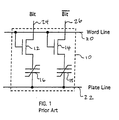
- In FIG. 1, a two-transistor two capacitor ("2T-2C")
ferroelectric memory cell 10 is shown.Ferroelectric memory cell 10 includes twoMOS transistors ferroelectric capacitors 16 and 18. The data state ofmemory cell 10 is determined by the opposite polarization states offerroelectric capacitors 16 and 18, as is explained in further detail below. A "one" data state may be represented by an "up" polarization state inferroelectric capacitor 16 and a "down" polarization state in ferroelectric capacitor 18, whereas a "zero" data state may be represented by a "down" polarization state inferroelectric capacitor 16 and an "up" polarization state in ferroelectric capacitor 18. The correlation between memory cell data states and the polarization of the ferroelectric capacitors in the memory cell is arbitrary and may be changed.Capacitors 16 and 18 must have opposite polarization directions for a valid data state, however. - The gate electrodes of
access transistors word line 20, which is also coupled to other ferroelectric memory cells (not shown in FIG. 1) in a row of an array of such cells.Word line 20 selectively energizesaccess transistors ferroelectric capacitors 16 and 18 to a differential bit line consisting of a bit line 24 and an invertedbit line 26. Bit line 24 and invertedbit line 26 are also coupled to other ferroelectric memory cells (not shown in FIG. 1) in a column of an array of such cells. Bit line 24 andbit line 26 receive the charge developed by poling (voltage pulsing)ferroelectric capacitors 16 and 18, which is later developed into a full logic voltage differential signal, usually five volts and ground.Ferroelectric capacitors 16 and 18 are also coupled to anactive plate line 22, which is also coupled to other ferroelectric memory cells (also not shown in FIG. 1) in a row of an array of such cells. - The operation of a ferroelectric capacitor such as
ferroelectric capacitor 16 or 18 inmemory cell 10 is illustrated in FIGS. 2A-D by way of a series of hysteresis loop diagrams 28A-D and corresponding voltage waveform diagrams 38A-D. Hysteresis loop diagrams 28A-D show the electrical performance of a ferroelectric capacitor, wherein the x-axis represents the voltage applied across the capacitor, and the y-axis represents the charge evolved by the ferroelectric capacitor in response to the applied voltage. Corresponding waveform diagrams 38A-D are a series of two positive voltage pulses and two negative voltage pulses that are applied across a ferroelectric capacitor in a known sequence that illustrates the complete electrical behavior of a ferroelectric capacitor. - Hysteresis loop diagram 28A of FIG. 2A includes a
hysteresis loop 30 and aninitial operating point 32.Operating point 32 represents a ferroelectric capacitor having, by convention, an "up" polarization state, but with no applied voltage across the capacitor. Theinitial operating point 32 is achieved by a previous application and removal of a negative applied voltage across the capacitor. The operating point of the ferroelectric capacitor moves fromoperating point 32 tooperating point 34 upon the application of a positive voltage pulse.Operating point 34 represents a fully saturated ferroelectric capacitor operating condition, i.e. further increases in applied voltage do not yield an appreciable amount of extra charge. The amount of charge evolved fromoperating point 32 to operating point 34 (the difference in the y-axis values) is designated "P". The "P" charge is termed a "switched charge" because the application of the external voltage pulse switches the polarization state of the ferroelectric capacitor. The leading edge of the first positive pulse in waveform diagram 38A is also labeled "P". Once the positive "P" pulse is removed, the operating point moves alonghysteresis loop 30 from operating point to 34 tooperating point 36. The amount of charge evolved fromoperating point 34 tooperating point 36 is designated "Pa" (for "P"-after). The "Pa" charge is termed a "linear charge" because the removal of the external voltage pulse does not switch the polarization state of the ferroelectric capacitor, and the charge evolved by the capacitor is approximately linearly related to the applied voltage. - Hysteresis loop diagram 28B of FIG. 2B includes a
hysteresis loop 30 and aninitial operating point 36.Operating point 36 represents a ferroelectric capacitor having, by convention, a "down" polarization state, but with no applied voltage across the capacitor. The operating point of the ferroelectric capacitor moves fromoperating point 36 tooperating point 34 upon the application of a second positive voltage pulse. The amount of charge evolved fromoperating point 36 tooperating point 34 is designated "U", and it is a linear charge. The leading edge of the second positive pulse in waveform diagram 38B is also labeled "U". Once the positive "U" pulse is removed, the operating point moves alonghysteresis loop 30 from operating point to 34 back tooperating point 36. The amount of charge evolved fromoperating point 34 tooperating point 36 is designated "Ua" (for "U"-after) and is approximately equal to the "U" and "Pa" charge components. - Hysteresis loop diagram 28C of FIG. 2C includes a
hysteresis loop 30 and aninitial operating point 36. The operating point of the ferroelectric capacitor moves fromoperating point 36 tooperating point 40 upon the application of a first negative voltage pulse. The amount of charge evolved fromoperating point 36 tooperating point 40 is designated "N", and it is a switched charge. The leading edge of the first negative pulse in waveform diagram 38C is also labeled "N". Once the negative "N" pulse is removed, the operating point moves alonghysteresis loop 30 from operating point to 40 back to theinitial operating point 32. The amount of charge evolved fromoperating point 40 to theinitial operating point 32 is designated "Na" (for "N"-after). - Hysteresis loop diagram 28D of FIG. 2D includes a
hysteresis loop 30 and aninitial operating point 32. The operating point of the ferroelectric capacitor moves fromoperating point 32 tooperating point 40 upon the application of a second negative voltage pulse. The amount of charge evolved fromoperating point 32 tooperating point 40 is designated "D", and it is a linear charge. The leading edge of the second negative pulse in waveform diagram 38D is also labeled "D". Once the negative "D" pulse is removed, the operating point moves alonghysteresis loop 30 from operating point to 40 back tooperating point 32. The amount of charge evolved fromoperating point 40 tooperating point 32 is designated "Da" (for "D"-after) and is approximately equal to the "D" and "Na" charge components. - Referring again to FIG. 2E, a ferroelectric material or capacitor is said to be "fully saturated" at
operating points hysteresis loop 30. The corresponding externally applied voltage at the saturation points is defined as "Vsat", for saturation voltage. Applying an external voltage beyond the saturation voltage results in extensions of thehysteresis loop hysteresis loop 30 shown in FIG. 2E. A typical ferroelectric dielectric material used for ferroelectric capacitors is lead zirconate titanate ("PZT"). If the PZT material is used, the saturation voltage, Vsat, is about five volts. For full saturation, an externally applied voltage pulse of about six to seven volts is used. This will ensure that virtually all of the ferroelectric domains in the material have switched, with operating points alongsections hysteresis loop 30. For partial saturation, which is operation on a sub-loop with voltages less than the saturation voltage, a voltage pulse of about four volts is used. A four volt pulse ensures that, while the ferroelectric material is not completely saturated, a sufficient quantity of charge is evolved that can be detected by conventional memory sense circuitry. - Referring now to FIG. 3, a waveform diagram shows the word line (WL), plate line (PL) and combined bit/inverted bit line (BIT and /BIT) waveforms associated with the reading and restore operation of the 2T-2C
ferroelectric memory cell 10 of FIG. 1. At time t1, all three signals are at a logic zero or ground potential. At time t2, the WL signal is energized to a logic one potential, usually five volts. With the WL signal at logic one, the gate electrodes ofaccess transistors inverted bit lines 24 and 26. The charge components are shown in the bit line waveform aslevels 44 and 46, which correspond to charge components P and U. At time t4 the PL pulse is removed, and the bit line charge is modified. The P charge component 44 is modified by the subtraction of the Pa charge component, leaving a charge equal to (P-Pa) shown in the bit line waveform aslevel 45. TheU charge component 46 is also modified by the subtraction of the Ua charge component, leaving a very small charge shown in the bit line waveform aslevel 47. Once thecharge levels ferroelectric memory cell 10. At time t7, the PL signal is returned to a logic zero state, and at time t8, the WL signal is returned to a logic zero state.Ferroelectric memory cell 10 is now returned to the same quiescent state that existed at time t1, and is ready for another read and restore cycle. The reading/sensing/restoring operation demonstrated with respect to FIG. 3 is known in the prior art as the "up-down" sensing method, since the plate line must be transitioned up and back down before the bit line charge is sensed and converted into full logic levels. - The same word line and plate line signals shown in FIG. 3 can be used for a writing operation. The only difference is that prior to the sensing operation,
bit lines 24 and 26 are written to, i.e. forced to receive a data state that may be the same or opposite tolevels - Whether
memory cell 10 is being read and restored, or written to, it is important to note that in the prior art that the first and second plate line pulses are the same voltage magnitude, about five volts. The first pulse is used to read the data state ofmemory cell 10 and has a pulsed voltage of about five volts. The second plate line pulse is used either restore the originally read data state, or to write a new data state tomemory cell 10. In either case, in the prior art, the second pulse also has a pulsed voltage of about five volts. - The reading, restoring, and writing operations described above with respect to FIGS. 1-3 adequately exercise
ferroelectric memory cell 10 such that it operates as a non-volatile memory cell. However, when operated for a long period of time,memory cell 10 eventually loses its ability to retain data. Various mechanisms such as compensation from mobile ions within the ferroelectric dielectric material inferroelectric capacitors 16 and 18 are thought to be at least partially responsible for the lack of data retention. - What is desired is another method of operating
memory cell 10 so that data retention performance can be extended beyond that which is possible with the current prior art technique described above. - It is desirable to improve the data retention performance of a ferroelectric memory.
- It is also desirable to extend the useful life of a ferroelectric memory.
- It is also desirable to improve the yield of a ferroelectric memory.
- It is an advantage of the invention that the improved method can be practiced without significantly increasing the die size of the ferroelectric memory integrated circuit.
- The present invention provides a method of operating a nonvolatile ferroelectric memory cell as set out in
claim 1. - The invention also provides a method of operating a nonvolatile ferroelectric memory cell as set out in
claim 4. - The method can be practiced on either a one transistor-one capacitor ("1T-1C") or a two transistor-two capacitor ("2T-2C") ferroelectric memory cell. During a read and restore operation of an embodiment, the plate line of the memory cell is pulsed with first and second voltage pulses that each have a voltage magnitude less than the normal five volt logic pulse, for example four volts, if PZT ferroelectric material is used. During a write operation of an embodiment, the plate line of the memory cell is pulsed with a voltage that has a magnitude greater than the normal five volt logic pulse, for example six to seven volts if PZT ferroelectric material is used. The combination of low voltage and high voltage plate line pulses preserves the retention ability of the ferroelectric memory cell.
- The normal ferroelectric memory architecture may be modified to include a charge pump/voltage regulator circuit in combination with the plate line and word line driver circuits, as well as other timing circuits, for selectively applying the required ground, low, and high voltages to the word and plate lines.
- The foregoing and other objects, features and advantages of the invention will become more readily apparent from the following detailed description of a preferred embodiment of the invention which proceeds with reference to the accompanying drawings.
-
- FIG. 1 is a schematic diagram of a prior art 2T-2C ferroelectric memory cell including distinct word, plate, and bit lines;
- FIGS. 2A-D are a series of four hysteresis loop diagrams and four corresponding waveform timing diagrams that serve to illustrate the electrical performance of a ferroelectric capacitor;
- FIG. 2E is a diagram of a hysteresis loop and a sub-loop for defining the saturation voltage of a ferroelectric material;
- FIG. 3 is a timing diagram illustrating the prior art "up-down" method of reading, sensing, and restoring a ferroelectric memory cell;
- FIG. 4A is a timing diagram illustrating a method of reading and writing a ferroelectric memory cell according to an embodiment of the present invention;
- FIG. 4B is a timing diagram illustrating a method of reading and restoring a ferroelectric memory cell according to an embodiment of the present invention;
- FIG. 5 is a block diagram of a ferroelectric memory architecture modified to effect the method of an embodiment of the present invention;
- FIGS. 6A and 6B are schematic/block diagrams of two embodiments of a charge pump block shown in FIG. 5 capable of generating low and high voltages as required in the method of the embodiment of the present invention; and
- FIG. 7 is a graph of ferroelectric memory integrated circuit yield versus time for selected combinations of read and write voltages.
-
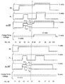
- Referring now to FIGS. 4A and 4B, two sets of waveform diagram each include word line (WL), plate line (PL), combined bit/inverted bit line (BIT and /BIT) waveforms, as well as a "Charge Pump Voltage" waveform associated with the reading and writing operation (FIG. 4A), and the reading and restoring operation (FIG. 4B) of the 2T-2C
ferroelectric memory cell 10 of FIG. 1. The Charge Pump Voltage indirectly controls the voltage levels of the plate line pulses and the word line pulse as is described in further detail below with respect to FIGS. 5, 6A and 6B. - Referring now specifically to FIG. 4A, at time t1, the WL, PL, and bit line signals are at a logic zero or ground potential. In addition, the Charge Pump Voltage is at about four volts, or one volt lower than the nominal supply voltage of five volts. At time t2, the WL signal is energized to a logic one potential, but at the Charge Pump Voltage level of four volts. The four volt WL signal is still sufficient to energize the gate electrodes of
access transistors inverted bit lines 24 and 26. The charge components are shown in the bit line waveform aslevels hysteresis loop 30 of theferroelectric capacitors 16 and 18. At time t4 the PL pulse is removed, and the bit line charges are modified as in the prior art scheme, but from the diminished levels corresponding to the four volt plate line pulse. Once the modifiedcharge levels ferroelectric memory cell 10 by fully saturatingmemory cell capacitors 16 and 18. At time t8, the PL signal is returned to a logic zero state, and at time t9, the WL signal is returned to a logic zero state. At time t10, the Charge Pump Voltage is returned to the original four volt value.Ferroelectric memory cell 10 is now returned to the same quiescent state that existed at time t1, and is ready for another read and write cycle. - The improved reading and writing operation described with respect to FIG. 4A has been empirically shown to improve the retention characteristics of
memory cell 10. The retention improvement is explained in further detail with respect to FIG. 7 below. - A reading and restoring operation is shown in FIG. 4B, in which the
ferroelectric capacitors 16 and 18 are not fully saturated. The operation proceeds identically as the reading and writing operation of FIG. 4A until time t4. Also, no data is forced onto the bit lines, the only charge being present arecharge components ferroelectric memory cell 10 by partially saturatingmemory cell capacitors 16 and 18. At time t7, the PL signal is returned to a logic zero state, and at time t8, the WL signal is returned to a logic zero state. At time t9, the bit lines are reset andferroelectric memory cell 10 is now returned to the same quiescent state that existed at time t1, and is ready for another read and restore cycle. - In FIGS. 4A and 4B, the total cycle time depicted is about 250 nanoseconds, with the write pulse in FIG. 4A and the restore pulse in FIG. 4B having a pulse width of about 20 nanoseconds. The pulsewidth of the initial read pulse is about the same as the write and restore pulse.
- The
architecture 56 for a ferroelectric memory integrated circuit that is capable of carrying out the method of the present embodiment of the invention is shown in FIG. 5. Most of the functional blocks shown in the block diagram of FIG. 5 are conventional to DRAM and ferroelectric memory design, with the exception of charge pump/regulator block 68, which is described in further detail below. - An edge detection/control latch block 66 is used to detect and determine valid transitions on the Chip Enable (CE), Write Enable (WE), and the Output Enable (OE) inputs. The signals are valid when they transition from a logic one to a logic zero level and are held at logic zero for about 15 ns. The control latches capture the valid signals and hold them until a functional cycle is completed. A
block 58 of address latches captures and holds the address when the chip enable signal is detected as valid.Address latch block 58 receives the addresses on address bus designated A0-AX. A latched output address (AL) is held at the output oflatch block 58. A column/row decoder 60 receives the latched address AL and selects the proper column in the memory array from the address that are captured at the start of the functional cycle. The column decode signal (COLDEC) is presented to an array 62 of ferroelectric memory cells arranged in rows and columns. The row decoder portion selects the proper word line and plate line that access memory array 62 from the address captured at the start of the cycle. The row decoder portion generates a row decode signal (ROWDEC). A block of clock timers 63 is controlled by the initiation of a chip enable latched signal (CEL) at the start of a valid read/restore or read/write cycle. The clock timer block 63 generates the proper pulse sequence to ablock 64 of wordline and plateline drivers. Wordline andplateline driver block 64 is further controlled by the ROWDEC signal to provide the appropriate word line (WL) and plate line (PL) signals to the selected row of ferroelectric memory cells. - A charge pump/regulator 68 supplies a dual value supply voltage, VCP, to word line drivers, plate line drivers in
block 64 and to the bit lines in the memory array 62 viasense amplifier block 72. The external Vcc power supply received by the ferroelectric memory integrated circuit is nominally five volts. The Vcc power supply voltage is stepped down to about four volts at the start and end of any functional cycle and applied to the proper circuits by the internal charge pump voltage (Vcp). If the function is a read, the write detect signal (WD) remains low and the Vcp level remains at four volts. If the function is a write, acontrol logic block 70 sets the WD signal to a logic one and activates the charge pump/regulator 68. Charge pump/regulator 68 step up the Vcp signal to about 6.5V and holds that level until the write pulse sequence is completed. The WD signal is released bycontrol logic block 70 and the Vcp signal is stepped back to about four volts. - I/O buffers 74 receive and drives the data to and from the memory. I/O buffers 74 are controlled by the state of the control latches 66 by signal OEL. During a read operation, I/O buffers 74 are placed in a mode to receive data (OUTDAT) from the array 62 through
sense amplifiers 72. During a write, I/O buffers 74 are placed in a mode to receive data from the I/O pads and pass this data (INDAT) to array 62 throughsense amplifiers 72.Sense amplifiers 72 receives complementary data from the bit lines of memory array 62. One sense amplifier compares the two levels on each differential bit line and determines the state of individual ferroelectric memory cells. The state of each individual memory cell is restored after it is read. During a read operation, data is transferred fromsense amplifiers 72 to the I/O buffer 74 by the Outdat signal. In the write mode, the data from the I/O buffers overdrives thesense amplifiers 72 with the Indat signals.Sense amplifiers 72 forces the data onto the bit lines to be stored into the cells using the write timing sequence. - The charge pump/regulator 68 is a means for supplying the selectable power supply voltage Vcp to the word and
plate line drivers 64. The charge pump/regulator block 68 is shown in further detail in FIGS. 6A and 6B. In FIG. 6A, charge pump/regulator 68A is the combination of acharge pump 78 and a voltage regulator 76. Voltage regulator 76 has an input for receiving the Vcc five volt power supply voltage and an output for generating a regulated four volt output voltage onconductor 77A.Charge pump 78 has an input also coupled to the Vcc five volt supply, and an output for generating a boosted voltage between six and seven volts onconductor 79. Amultiplexer 80 has first and second inputs coupled to the outputs of voltage regulator 76 andcharge pump 78, a third control input receiving the WD control signal atnode 75, and an output for supplying the selectable Vcp power supply voltage atnode 81. - An alternative means 68B for supplying the Vcp power supply voltage is shown in FIG. 6B. In certain cases, a voltage regulator 76 can be omitted if the Vcc power supply voltage is low enough to only partially saturate the ferroelectric capacitors in the ferroelectric memory array of the integrated circuit. For example, an integrated circuit may have a 3.3 volt power supply voltage. This 3.3 volt power supply voltage could be fed directly into
multiplexer 80 onconductor 77B without the necessity of an intervening voltage regulator 76. The resulting dual level Vcp output voltage atnode 81 would have voltage levels of 3.3 volts and six volts. For this combination of voltages to be useful, the ferroelectric material used would have to be partially saturated at 3.3 volts and generating enough charge to be conventionally sensed. - FIG. 7 is a
graph 88 of ferroelectric memory integrated circuit yield versus time for selected combination of read and write voltages. The varying yields illustrated are primarily impacted by retention performance. Five different write/read voltage combinations were used, with the resulting data points (letters) and graph traces (dashed and solid lines) according to the following table:Trace No. Data Letter Write Voltage Read Voltage 89 A 4.0 volts 4.0 volts 90 B 4.0 volts 6.0 volts 91 C 6.0 volts 4.0 volts 92 D 6.0 volts 6.0 volts 93 E 5.0 volts 5.0 volts graph 88, after initially being parametrically tested and programmed with a predetermined data pattern. The accelerated time of ten hours (first data point) at 150 ° C is equivalent to about four years at 70 ° C or twenty five years at 55 ° C. The memory was then tested at the first data point to determine whether or not the initial stored pattern was retained. With a four volt read pulse and six volt write pulse, the yield at the first data point is about 83%, the highest of all write/read voltages used. The yield (that is, number of good integrated circuit die divided by total die tested) was subsequently recorded at three other data points at 35 hours, about 60 hours, and about 107 hours. The four volt read/six volt write pulse combination demonstrated the best yield at all of the remaining data points. - Having described and illustrated the principles of the invention in a preferred embodiment thereof, it is appreciated by those having skill in the art that the invention can be modified in arrangement and detail without departing from such principles. For example, other ferroelectric materials can be used, such as lanthanum doped PZT ("PLZT"), bismuth titanate, as well as many others, in which case the corresponding low and high voltage values of Vcp would be modified according to the saturation voltage of the ferroelectric material. We therefore claim all modifications and variation coming within the scope of the following claims.
Claims (20)
- A method of operating a nonvolatile ferroelectric memory cell including a polarized ferroelectric capacitor, the method comprising the steps of:during a read operation, reading and restoring a first polarization state of the ferroelectric capacitor at a voltage not sufficient to fully saturate the ferroelectric capacitor, but sufficient to release a detectable amount of charge corresponding to the first polarization state; andduring a write operation, writing a second polarization state in the ferroelectric capacitor at a voltage sufficient to fully saturate the ferroelectric capacitor.
- The method of claim 1 in which the reading and restoring step comprises the steps of:applying a first voltage pulse across the ferroelectric capacitor;sensing the charge on the ferroelectric capacitor; andapplying a second voltage pulse across the ferroelectric capacitor, the first and second voltage pulses being of a magnitude insufficient to fully saturate the ferroelectric capacitor.
- The method of claim 1 in which the writing step comprises the step of applying a voltage pulse across the ferroelectric capacitor sufficient to fully saturate the ferroelectric capacitor.
- A method of operating a nonvolatile ferroelectric memory cell including a pair of polarized ferroelectric capacitors (16,18), a differential bit line (24,26), a word line (20), and a plate line (22), the method comprising the steps of:in a read operation,pulsing the plate line (22) with a first voltage pulse not sufficient to fully saturate the ferroelectric capacitors (16,18), but sufficient to release a detectable amount of charge onto the differential bit line (24,26) corresponding to a first data state,resolving the charge on the differential bit line (24, 26), andpulsing the plate line (22) with a second voltage pulse not sufficient to fully saturate the ferroelectric capacitors (16,18) but sufficient to restore the first data state;in a write operation,pulsing the plate line (22) with a first voltage pulse not sufficient to fully saturate the ferroelectric capacitors (16,18),forcing a charge on the differential bit line (24,26) corresponding to a desired second data state,resolving the charge on the differential bit line (24,26), andpulsing the plate line (22) with a second voltage pulse sufficient to fully saturate the ferroelectric capacitors (16,18) to establish the second data state.
- The method of claim 4 in which the pulsing steps carried out at the voltage not sufficient to fully saturate the ferroelectric capacitors (16,18) each comprise the step of pulsing the plate line (22) with a voltage of about four volts.
- The method of claim 4 in which the pulsing step carried out at the voltage sufficient to fully saturate the ferroelectric capacitors (16,18) comprises the step of pulsing the plate line with a voltage of about six to seven volts.
- The method of claim 4 further comprising the step of pulsing the word line (20) with a voltage pulse having a first low voltage portion and a second higher voltage portion during the write operation.
- The method of claim 7 in which the first low voltage portion occurs during the first plate line voltage pulse, and the second higher voltage portion occurs during the second plate line voltage pulse.
- The method of claim 4 further comprising the step of pulsing the word line (20) with a voltage pulse having a four volt portion and a six volt portion during the write operation.
- The method of claim 4 in which:the resolving step during the read operation comprises the step of converting the differential bit line charge into a first low voltage differential logic signal; andthe resolving step during the write operation comprises the step of converting the differential bit line charge into a second higher voltage differential logic signal.
- The method of claim 10 in which the resolving step during the read operation comprises the step of converting the differential bit line charge into a four volt differential logic signal.
- The method of claim 10 in which the resolving step during the write operation comprises the step of converting the differential bit line charge into a six to seven volt differential logic signal.
- A ferroelectric memory comprising:a ferroelectric memory cell (62) including a ferroelectric capacitor, a word line, a plate line, and a bit line; andmeans (64) for selectively applying a ground voltage, a first low voltage and a second, high voltage to the word and plate lines, said first low voltage being insufficient to fully saturate the ferroelectric capacitor and said second high voltage being sufficient to fully saturate the ferroelectric capacitor.
- A ferroelectric memory as in claim 13 in which the means (64) for selectively applying a ground voltage, a first low voltage and a second, high voltage to the word and plate lines comprises:means for selectively supplying either a low voltage pulse or a pulse having a first low voltage portion and a second high voltage portion to the word line; andmeans for selectively supplying either first and second low voltage pulses or a first low voltage pulse and a second high voltage pulse to the plate line.
- A ferroelectric memory as in claim 13 in which the first low voltage is about four volts and the second, high voltage is about six to seven volts.
- A ferroelectric memory as in claim 13 in which the means (64) for selectively applying a ground voltage, a first low voltage and a second, high voltage comprises:a word line driver coupled to the word line;a plate line driver coupled to the plate line; andmeans (68) for supplying a selectable power supply voltage to the word and plate line drivers.
- A ferroelectric memory as in claim 16 in which the means (68A) for supplying a selectable power supply voltage to the word and plate line drivers comprises the combination of a charge pump (78) and a voltage regulator (76).
- A ferroelectric memory as in claim 16 in which the means for supplying a selectable power supply voltage to the word and plate line drivers comprises:a voltage regulator (76) having an input for receiving a power supply voltage and an output;a charge pump (78) having an input for receiving a power supply voltage and an output; anda multiplexer (80) having first and second inputs coupled to the outputs of the voltage regulator and charge pump, a third input receiving a control signal, and an output for supplying the selectable power supply voltage.
- A ferroelectric memory as in claim 16 in which the means for supplying a selectable power supply voltage to the word and plate line drivers comprises:a charge pump (78) having an input for receiving a power supply voltage and an output; anda multiplexer (80) having first and second inputs for receiving the power supply voltage and the output of the charge pump, a third input receiving a control signal, and an output for supplying the selectable power supply voltage.
- A ferroelectric memory as in claim 13 in which the memory cell is part of an array (62) of such cells arranged in rows and columns.
Applications Claiming Priority (2)
| Application Number | Priority Date | Filing Date | Title |
|---|---|---|---|
| US413083 | 1995-03-29 | ||
| US08/413,083 US5532953A (en) | 1995-03-29 | 1995-03-29 | Ferroelectric memory sensing method using distinct read and write voltages |
Publications (3)
| Publication Number | Publication Date |
|---|---|
| EP0735541A2 EP0735541A2 (en) | 1996-10-02 |
| EP0735541A3 EP0735541A3 (en) | 1998-07-22 |
| EP0735541B1 true EP0735541B1 (en) | 2001-06-13 |
Family
ID=23635749
Family Applications (1)
| Application Number | Title | Priority Date | Filing Date |
|---|---|---|---|
| EP96301669A Expired - Lifetime EP0735541B1 (en) | 1995-03-29 | 1996-03-12 | Ferroelectric memory sensing method using distinct read and write voltages |
Country Status (4)
| Country | Link |
|---|---|
| US (1) | US5532953A (en) |
| EP (1) | EP0735541B1 (en) |
| JP (1) | JP3200009B2 (en) |
| DE (1) | DE69613266T2 (en) |
Families Citing this family (38)
| Publication number | Priority date | Publication date | Assignee | Title |
|---|---|---|---|---|
| KR100333153B1 (en) * | 1993-09-07 | 2002-12-05 | 가부시키가이샤 한도오따이 에네루기 켄큐쇼 | Process for fabricating semiconductor device |
| JPH07109573A (en) * | 1993-10-12 | 1995-04-25 | Semiconductor Energy Lab Co Ltd | Glass substrate and heat treatment |
| US5682344A (en) * | 1995-09-11 | 1997-10-28 | Micron Technology, Inc. | Destructive read protection using address blocking technique |
| TW322578B (en) * | 1996-03-18 | 1997-12-11 | Matsushita Electron Co Ltd | |
| US5703804A (en) * | 1996-09-26 | 1997-12-30 | Sharp Kabushiki K.K. | Semiconductor memory device |
| US5990513A (en) * | 1996-10-08 | 1999-11-23 | Ramtron International Corporation | Yield enhancement technique for integrated circuit processing to reduce effects of undesired dielectric moisture retention and subsequent hydrogen out-diffusion |
| KR100206713B1 (en) * | 1996-10-09 | 1999-07-01 | 윤종용 | Nondestructive accessing method of ferroelectric memory device and its accessing circuit |
| KR100248355B1 (en) * | 1997-04-09 | 2000-03-15 | 김영환 | Variable comparision voltage generating circuit of semiconductor memory device |
| US6118688A (en) * | 1997-06-05 | 2000-09-12 | Matsushita Electronics Corporation | Ferroelectric memory device and method for driving it |
| WO1999000798A1 (en) * | 1997-06-27 | 1999-01-07 | Matsushita Electronics Corporation | Ferroelelectric memory device and method of driving the same |
| KR100297874B1 (en) | 1997-09-08 | 2001-10-24 | 윤종용 | Ferroelectric random access memory device |
| KR100252052B1 (en) * | 1997-12-03 | 2000-04-15 | 윤종용 | Evaluation method of ferroelectric memory device using cell test pattern |
| US6157979A (en) * | 1998-03-14 | 2000-12-05 | Advanced Technology Materials, Inc. | Programmable controlling device with non-volatile ferroelectric state-machines for restarting processor when power is restored with execution states retained in said non-volatile state-machines on power down |
| US6242299B1 (en) | 1999-04-01 | 2001-06-05 | Ramtron International Corporation | Barrier layer to protect a ferroelectric capacitor after contact has been made to the capacitor electrode |
| US6219270B1 (en) * | 1999-05-24 | 2001-04-17 | U.S. Philips Corporation | Integrated circuit having dynamic memory with boosted plateline |
| JP2001093286A (en) * | 1999-09-21 | 2001-04-06 | Nec Corp | Ferroelectric storage device and its manufacturing method |
| JP3916837B2 (en) * | 2000-03-10 | 2007-05-23 | 株式会社東芝 | Ferroelectric memory |
| KR100382546B1 (en) * | 2000-12-04 | 2003-05-09 | 주식회사 하이닉스반도체 | Nonvolatile ferroelectric memory device and method for detecting weak cell using the same |
| JP2002269972A (en) * | 2000-12-27 | 2002-09-20 | Seiko Epson Corp | Semiconductor memory, and operating method for memory cell consisting of ferroelectric capacitors |
| US6535446B2 (en) | 2001-05-24 | 2003-03-18 | Ramtron International Corporation | Two stage low voltage ferroelectric boost circuit |
| US6430093B1 (en) | 2001-05-24 | 2002-08-06 | Ramtron International Corporation | CMOS boosting circuit utilizing ferroelectric capacitors |
| JP4024166B2 (en) * | 2002-03-20 | 2007-12-19 | 三洋電機株式会社 | Ferroelectric memory |
| JP3650077B2 (en) * | 2002-03-29 | 2005-05-18 | 沖電気工業株式会社 | Semiconductor memory device |
| US6741504B2 (en) * | 2002-07-19 | 2004-05-25 | Micron Technology, Inc. | Method and apparatus for reducing gate-induced diode leakage in semiconductor devices |
| KR100469153B1 (en) * | 2002-08-30 | 2005-02-02 | 주식회사 하이닉스반도체 | Ferroelectric memory device |
| KR100492800B1 (en) * | 2002-11-12 | 2005-06-07 | 주식회사 하이닉스반도체 | Device for controlling non-volatile ferroelectric memory |
| JP2004220705A (en) * | 2003-01-15 | 2004-08-05 | Seiko Epson Corp | Ferroelectric storage device |
| JP4041054B2 (en) * | 2003-11-06 | 2008-01-30 | 株式会社東芝 | Semiconductor integrated circuit device |
| JP4511377B2 (en) * | 2005-01-28 | 2010-07-28 | パナソニック株式会社 | Ferroelectric memory device |
| JP4667888B2 (en) * | 2005-02-01 | 2011-04-13 | パナソニック株式会社 | Semiconductor memory device |
| KR100694406B1 (en) * | 2005-04-21 | 2007-03-12 | 주식회사 하이닉스반도체 | Non-volatile ferroelectric memory device with circuit for processing fail cell and control method therefor |
| US7609559B2 (en) * | 2007-01-12 | 2009-10-27 | Micron Technology, Inc. | Word line drivers having a low pass filter circuit in non-volatile memory device |
| US9092582B2 (en) | 2010-07-09 | 2015-07-28 | Cypress Semiconductor Corporation | Low power, low pin count interface for an RFID transponder |
| US9846664B2 (en) | 2010-07-09 | 2017-12-19 | Cypress Semiconductor Corporation | RFID interface and interrupt |
| US8723654B2 (en) | 2010-07-09 | 2014-05-13 | Cypress Semiconductor Corporation | Interrupt generation and acknowledgment for RFID |
| US8842460B2 (en) | 2012-11-26 | 2014-09-23 | Cypress Semiconductor Corporation | Method for improving data retention in a 2T/2C ferroelectric memory |
| US9361972B1 (en) * | 2015-03-20 | 2016-06-07 | Intel Corporation | Charge level maintenance in a memory |
| US9697882B1 (en) * | 2016-08-30 | 2017-07-04 | Radiant Technologies, Inc. | Analog ferroelectric memory with improved temperature range |
Family Cites Families (3)
| Publication number | Priority date | Publication date | Assignee | Title |
|---|---|---|---|---|
| US5270967A (en) * | 1991-01-16 | 1993-12-14 | National Semiconductor Corporation | Refreshing ferroelectric capacitors |
| FR2688090B1 (en) * | 1992-02-27 | 1994-04-08 | Commissariat A Energie Atomique | NON-VOLATILE MEMORY CELL OF THE SEMICONDUCTOR METAL-FERROELECTRIC TYPE. |
| US5309391A (en) * | 1992-10-02 | 1994-05-03 | National Semiconductor Corporation | Symmetrical polarization enhancement in a ferroelectric memory cell |
-
1995
- 1995-03-29 US US08/413,083 patent/US5532953A/en not_active Expired - Fee Related
-
1996
- 1996-03-12 EP EP96301669A patent/EP0735541B1/en not_active Expired - Lifetime
- 1996-03-12 DE DE69613266T patent/DE69613266T2/en not_active Expired - Fee Related
- 1996-03-29 JP JP07659496A patent/JP3200009B2/en not_active Expired - Fee Related
Also Published As
| Publication number | Publication date |
|---|---|
| EP0735541A3 (en) | 1998-07-22 |
| DE69613266D1 (en) | 2001-07-19 |
| US5532953A (en) | 1996-07-02 |
| JP3200009B2 (en) | 2001-08-20 |
| JPH08273375A (en) | 1996-10-18 |
| EP0735541A2 (en) | 1996-10-02 |
| DE69613266T2 (en) | 2001-09-20 |
Similar Documents
| Publication | Publication Date | Title |
|---|---|---|
| EP0735541B1 (en) | Ferroelectric memory sensing method using distinct read and write voltages | |
| US5847989A (en) | Ferroelectric memory using non-remnant reference circuit | |
| US5638318A (en) | Ferroelectric memory using ferroelectric reference cells | |
| US5680344A (en) | Circuit and method of operating a ferrolectric memory in a DRAM mode | |
| CN110741437B (en) | 2T1C ferroelectric random access memory cell | |
| US5999439A (en) | Ferroelectric memory using ferroelectric reference cells | |
| US5835400A (en) | Ferroelectric memory devices having nondestructive read capability and methods of operating same | |
| US6924997B2 (en) | Ferroelectric memory and method of operating same | |
| US6906944B2 (en) | Ferroelectric memory | |
| US7313011B2 (en) | Ferroelectric memory devices having a plate line control circuit | |
| US6704218B2 (en) | FeRAM with a single access/multiple-comparison operation | |
| US7307866B2 (en) | Ferroelectric memory and method for reading data from the ferroelectric memory | |
| US20010040814A1 (en) | Semiconductor memory device | |
| US5907861A (en) | Destructive read protection using address blocking technique | |
| KR19990024829A (en) | Ferroelectric Random Access Memory Device | |
| US6522568B1 (en) | Ferroelectric memory and method for reading the same | |
| JP2001338499A (en) | Ferroelectric memory device and resting method therefor | |
| US5892705A (en) | Apparatus for maintaining non-volatility in ferroelectric ramdom access memory and method therefor | |
| US5835399A (en) | Imprint compensation circuit for use in ferroelectric semiconductor memory device | |
| US6438020B1 (en) | Ferroelectric memory device having an internal supply voltage, which is lower than the external supply voltage, supplied to the memory cells | |
| KR100462085B1 (en) | Semiconductor memory circuit | |
| JP3717097B2 (en) | Ferroelectric memory | |
| US7009864B2 (en) | Zero cancellation scheme to reduce plateline voltage in ferroelectric memory | |
| US6310797B1 (en) | Drive method for FeRAM memory cell and drive device for the memory cell | |
| DE102005006343B4 (en) | Integrated semiconductor memory with isochronous access control |
Legal Events
| Date | Code | Title | Description |
|---|---|---|---|
| PUAI | Public reference made under article 153(3) epc to a published international application that has entered the european phase |
Free format text: ORIGINAL CODE: 0009012 |
|
| AK | Designated contracting states |
Kind code of ref document: A2 Designated state(s): DE GB |
|
| PUAL | Search report despatched |
Free format text: ORIGINAL CODE: 0009013 |
|
| AK | Designated contracting states |
Kind code of ref document: A3 Designated state(s): DE GB |
|
| 17P | Request for examination filed |
Effective date: 19980910 |
|
| 111Z | Information provided on other rights and legal means of execution |
Free format text: 19990412 DE GB |
|
| 17Q | First examination report despatched |
Effective date: 19991105 |
|
| GRAG | Despatch of communication of intention to grant |
Free format text: ORIGINAL CODE: EPIDOS AGRA |
|
| GRAG | Despatch of communication of intention to grant |
Free format text: ORIGINAL CODE: EPIDOS AGRA |
|
| GRAH | Despatch of communication of intention to grant a patent |
Free format text: ORIGINAL CODE: EPIDOS IGRA |
|
| GRAH | Despatch of communication of intention to grant a patent |
Free format text: ORIGINAL CODE: EPIDOS IGRA |
|
| GRAA | (expected) grant |
Free format text: ORIGINAL CODE: 0009210 |
|
| AK | Designated contracting states |
Kind code of ref document: B1 Designated state(s): DE GB |
|
| REF | Corresponds to: |
Ref document number: 69613266 Country of ref document: DE Date of ref document: 20010719 |
|
| REG | Reference to a national code |
Ref country code: GB Ref legal event code: IF02 |
|
| PG25 | Lapsed in a contracting state [announced via postgrant information from national office to epo] |
Ref country code: GB Free format text: LAPSE BECAUSE OF NON-PAYMENT OF DUE FEES Effective date: 20020312 |
|
| PLBE | No opposition filed within time limit |
Free format text: ORIGINAL CODE: 0009261 |
|
| STAA | Information on the status of an ep patent application or granted ep patent |
Free format text: STATUS: NO OPPOSITION FILED WITHIN TIME LIMIT |
|
| 26N | No opposition filed | ||
| PG25 | Lapsed in a contracting state [announced via postgrant information from national office to epo] |
Ref country code: DE Free format text: LAPSE BECAUSE OF NON-PAYMENT OF DUE FEES Effective date: 20021001 |
|
| GBPC | Gb: european patent ceased through non-payment of renewal fee |
Effective date: 20020312 |