EP0739125A2 - Improvements relating to a display and printing system and method - Google Patents
Improvements relating to a display and printing system and method Download PDFInfo
- Publication number
- EP0739125A2 EP0739125A2 EP96106193A EP96106193A EP0739125A2 EP 0739125 A2 EP0739125 A2 EP 0739125A2 EP 96106193 A EP96106193 A EP 96106193A EP 96106193 A EP96106193 A EP 96106193A EP 0739125 A2 EP0739125 A2 EP 0739125A2
- Authority
- EP
- European Patent Office
- Prior art keywords
- pixels
- illuminated
- light
- rows
- light modulator
- Prior art date
- Legal status (The legal status is an assumption and is not a legal conclusion. Google has not performed a legal analysis and makes no representation as to the accuracy of the status listed.)
- Withdrawn
Links
Images


Classifications
-
- G—PHYSICS
- G03—PHOTOGRAPHY; CINEMATOGRAPHY; ANALOGOUS TECHNIQUES USING WAVES OTHER THAN OPTICAL WAVES; ELECTROGRAPHY; HOLOGRAPHY
- G03G—ELECTROGRAPHY; ELECTROPHOTOGRAPHY; MAGNETOGRAPHY
- G03G15/00—Apparatus for electrographic processes using a charge pattern
- G03G15/04—Apparatus for electrographic processes using a charge pattern for exposing, i.e. imagewise exposure by optically projecting the original image on a photoconductive recording material
-
- H—ELECTRICITY
- H04—ELECTRIC COMMUNICATION TECHNIQUE
- H04N—PICTORIAL COMMUNICATION, e.g. TELEVISION
- H04N1/00—Scanning, transmission or reproduction of documents or the like, e.g. facsimile transmission; Details thereof
- H04N1/04—Scanning arrangements, i.e. arrangements for the displacement of active reading or reproducing elements relative to the original or reproducing medium, or vice versa
- H04N1/19—Scanning arrangements, i.e. arrangements for the displacement of active reading or reproducing elements relative to the original or reproducing medium, or vice versa using multi-element arrays
- H04N1/191—Scanning arrangements, i.e. arrangements for the displacement of active reading or reproducing elements relative to the original or reproducing medium, or vice versa using multi-element arrays the array comprising a one-dimensional array, or a combination of one-dimensional arrays, or a substantially one-dimensional array, e.g. an array of staggered elements
- H04N1/1911—Simultaneously or substantially simultaneously scanning picture elements on more than one main scanning line, e.g. scanning in swaths
- H04N1/1916—Simultaneously or substantially simultaneously scanning picture elements on more than one main scanning line, e.g. scanning in swaths using an array of elements displaced from one another in the main scan direction, e.g. a diagonally arranged array
-
- B—PERFORMING OPERATIONS; TRANSPORTING
- B41—PRINTING; LINING MACHINES; TYPEWRITERS; STAMPS
- B41J—TYPEWRITERS; SELECTIVE PRINTING MECHANISMS, i.e. MECHANISMS PRINTING OTHERWISE THAN FROM A FORME; CORRECTION OF TYPOGRAPHICAL ERRORS
- B41J2/00—Typewriters or selective printing mechanisms characterised by the printing or marking process for which they are designed
- B41J2/435—Typewriters or selective printing mechanisms characterised by the printing or marking process for which they are designed characterised by selective application of radiation to a printing material or impression-transfer material
- B41J2/465—Typewriters or selective printing mechanisms characterised by the printing or marking process for which they are designed characterised by selective application of radiation to a printing material or impression-transfer material using masks, e.g. light-switching masks
-
- G—PHYSICS
- G02—OPTICS
- G02B—OPTICAL ELEMENTS, SYSTEMS OR APPARATUS
- G02B26/00—Optical devices or arrangements for the control of light using movable or deformable optical elements
- G02B26/08—Optical devices or arrangements for the control of light using movable or deformable optical elements for controlling the direction of light
- G02B26/0816—Optical devices or arrangements for the control of light using movable or deformable optical elements for controlling the direction of light by means of one or more reflecting elements
- G02B26/0833—Optical devices or arrangements for the control of light using movable or deformable optical elements for controlling the direction of light by means of one or more reflecting elements the reflecting element being a micromechanical device, e.g. a MEMS mirror, DMD
-
- H—ELECTRICITY
- H04—ELECTRIC COMMUNICATION TECHNIQUE
- H04N—PICTORIAL COMMUNICATION, e.g. TELEVISION
- H04N1/00—Scanning, transmission or reproduction of documents or the like, e.g. facsimile transmission; Details thereof
- H04N1/04—Scanning arrangements, i.e. arrangements for the displacement of active reading or reproducing elements relative to the original or reproducing medium, or vice versa
- H04N1/19—Scanning arrangements, i.e. arrangements for the displacement of active reading or reproducing elements relative to the original or reproducing medium, or vice versa using multi-element arrays
- H04N1/195—Scanning arrangements, i.e. arrangements for the displacement of active reading or reproducing elements relative to the original or reproducing medium, or vice versa using multi-element arrays the array comprising a two-dimensional array or a combination of two-dimensional arrays
- H04N1/19505—Scanning picture elements spaced apart from one another in at least one direction
- H04N1/1951—Scanning picture elements spaced apart from one another in at least one direction in one direction
-
- H—ELECTRICITY
- H04—ELECTRIC COMMUNICATION TECHNIQUE
- H04N—PICTORIAL COMMUNICATION, e.g. TELEVISION
- H04N1/00—Scanning, transmission or reproduction of documents or the like, e.g. facsimile transmission; Details thereof
- H04N1/04—Scanning arrangements, i.e. arrangements for the displacement of active reading or reproducing elements relative to the original or reproducing medium, or vice versa
- H04N1/19—Scanning arrangements, i.e. arrangements for the displacement of active reading or reproducing elements relative to the original or reproducing medium, or vice versa using multi-element arrays
- H04N1/195—Scanning arrangements, i.e. arrangements for the displacement of active reading or reproducing elements relative to the original or reproducing medium, or vice versa using multi-element arrays the array comprising a two-dimensional array or a combination of two-dimensional arrays
- H04N1/19505—Scanning picture elements spaced apart from one another in at least one direction
- H04N1/19521—Arrangements for moving the elements of the array relative to the scanned image or vice versa
- H04N1/19526—Optical means
- H04N1/19547—Apertures
Definitions
- This invention generally relates to display and printer systems and specifically to a printing system which uses a staggered array spatial light modulator.
- electrophotography has become one of the most widely used systems and the dry toner process, has become the most popular for creating copies and prints of documents in a host of environments.
- the basics of electrophotography are well know to those skilled in the art.
- the fundamental elements of a electrophotographic printer or copier using the dry toner process include a photo sensitive medium, typically an organic photoreceptor (OPC), which is charged electrostatically to a predetermined voltage and polarity.
- OPC organic photoreceptor
- this image is passed by a source of developer materials which consists of electrostatically charged toner particles held to ferromagnetic carrier beads.
- the carriers are used to facilitate the transport of the materials into contact with the above mentioned latent image through the action of magnetic fields and rotating magnets within sleeved cylinders, typically called developer rollers.
- developer rollers Through a designed interplay of electrostatic charges, the toner particles that are typically in the 10 micron diameter range, are separated from the carrier beads, typically 50 micron diameter particles, and retained in-place on the appropriate portions of the latent image resident on the OPC surface.
- the magnetic forces associated with the developer rollers carry the depleted ferromagnetic carrier beads back to the position where they are re-mixed with additional toner for development of subsequent images.
- the toner materials are normally plastics with flow promoting agents, charge control agents, and color pigments which melt at a predetermined temperature.
- the OPC surface then carries a developed latent image after exiting the proximity of the developing roller.
- the photoreceptor surface carrying the developed image is brought into contact with an image receptor, which in most common applications of electrophotography is a sheet of paper, but may be an intermediate material suitable for the build-up of multiple pigmented images as required for color printing.
- Electrostatic charging systems are typically used to transfer the toner from the OPC to the image receptor.
- the final image bearing member is ultimately paper or an other material, it can be successively operated on by multiple photoreceptors, a single photoreceptor, or an image bearing intermediate member to build up the full color image. It exits the printing process through a station referred to as the fuser, where the appropriate heat and/or pressure is applied to the image receptor and thereby fixes the image permanently.
- a movable mirror device such as the Digital Micromirror Device (also referred to as Deformable Mirror Device or simply a DMD) manufactured by Texas Instruments, Inc.
- the movable mirror device is composed of many small mirrors called micromirrors which rotate about a fixed axis.
- the movable mirror device is illuminated with a beam of light.
- the rotation of the micromirror causes the light illuminating the micromirror to be deflected under the control of the rotation.
- each micromirror of a movable mirror device can be selectively rotated thereby patterning light reflected from the array.
- Specific details of movable mirror devices are provided in US Patent No. 5,061,049 and 5,083,857, each of which is incorporated herein by reference.
- a long and narrow movable mirror device When using a movable mirror device in print applications, a long and narrow movable mirror device will typically be used. As an example, a movable mirror device array with about 100 rows and 7,000 columns may be utilized. To produce a device of this size, the chip may typically be 5.0 inches long.
- a system for independently illuminating a plurality of areas on an object, such as a printer drum, is disclosed herein.
- the system includes a light source, such as a single light emitting diode (LED) or a plurality of LEDs.
- a spatial light modulator which may be a movable mirror device, such as the Digital Micromirror Device (DMD) manufactured by Texas Instruments, Inc., receives light from the light source and reflects selected portions of the light.
- the mirror device is illuminated in a scanning mode, i. e., each row of mirror elements is illuminated individually and sequentially by scanning a beam of light over all of the micromirrors.
- the mirror device is illuminated in a staring mode, i.e., all the mirror elements of the entire array are illuminated simultaneously.
- the light from the spatial light modulator is imaged onto the object to be illuminated which is partitioned into rows of pixels (picture elements).
- the object is illuminated in such a way that each pixel is, over time, illuminated by light from a corresponding column of micromirrors.
- An advantage of the invention is that it reduces the number of columns of micromirrors required by the movable mirror device. This reduction may be important in printing applications where the number of columns is very high resulting in physically large integrated circuit chips which are difficult to illuminate.
- the reduction in the size of the chip will reduce the cost to manufacture the chip as well as the cost of the optical subsystem to illuminate the chip thereby reducing the cost of the system which the chip subsequently is installed.
- a first embodiment of the staggered array printing system 10 is of the scan mode variety and is depicted in Figure 1A.
- a light source 12 such as a light laser diode, illuminates a spatial light modulator 14.
- the spatial light modulator 14 may comprise a movable mirror device such as the Digital Micromirror Device (DMD) manufactured by Texas Instruments and described in US Patents 5,061,049 and 5,083,857, incorporated herein by reference.
- DMD Digital Micromirror Device
- the light from the light source 12 is scanned over the movable mirror device by means of light scanning optics 13.
- the light illuminating the movable mirror device from the light source 12 forms a long and narrow beam on the movable mirror device.
- the length of the beam is equal to the length of the movable mirror device array and the width of the beam is equal to the width of the illuminated portion of micromirrors.
- each row of micromirrors of the movable mirror device array is sequentially illuminated.
- the beam is scanned rapidly enough that all of the mirror elements are illuminated during a time interval short enough that the illuminated object, such as a printer drum 26, turns only a small fraction of a pixel.
- Modulated light is reflected from the spatial light modulator 14 into projection lens 24 which images the light onto the drum 26.
- the lens 24 may be an anamorphic lens if it is desired to have a printing beam which is not the same shape as the micromirror.
- the rotating drum 26 may then transfer toner to a sheet of paper 27.
- the light scanning optics 13 comprises a first lens 18, a scanner 20, and a third lens 22.
- the scanner 20 scans the light beam down the array within the spatial light modulator 14 in the vertical direction successively illuminating the movable mirror device mirror elements in each row.
- FIG 1C depicts a staring mode embodiment of the staggered array printing system 10.
- the light source 12 such as a light emitting diode (LED) illuminates the spatial light modulator 14.
- the spatial light modulator 14 may comprise a movable mirror device such as the Digital Micromirror Device (DMD) manufactured by Texas Instruments and described in US Patents 5,061,049 and 5,083,857.
- DMD Digital Micromirror Device
- the light from the light source 12 is directed toward the movable mirror device by means of light directing optics 16.
- the light beam illuminates all of the micromirrors of the moving mirror device simultaneously.
- Modulated light is reflected from the spatial light modulator 14 into the projection lens 24 which images the light onto the drum 26.
- the light source 12 is pulsed (rapidly turned on and then off) at a period equal to that required by the drum 26 to rotate through one pixel.
- the light pulse will preferably have a 10% duty cycle so that a sharp image of the mirror element is formed on the drum 26 (i.e., the mirror element image is not "smeared" by the rotation of the drum).
- the lens 24 may be an anamorphic lens if it is desired to have a printing beam which is not the same shape as the micromirror.
- the rotating drum 26 may then transfer toner to the sheet of paper 27.
- the light source 12 is a linear array of LED emitters and the light directing optics 16 is a toroidal lens which magnifies the LED emitters so that the image of each emitter fills the DMD.
- the spatial light modulator 14 preferably comprises a movable mirror device such as the Digital Micromirror Device (DMD) manufactured by Texas Instruments, Inc.
- DMD Digital Micromirror Device
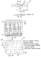
- This movable mirror device 14 is configured in a plurality of rows and columns as illustrated in Figure 2A.
- Each of the rows comprises a plurality of mirror elements (sometimes called micromirrors) 28.
- each row of mirror elements 28 is displaced in the horizontal direction by 1/3 of a mirror dimension.
- Each of the three rows will illuminate 1/3 of the object to be illuminated, e.g., the drum 26 as shown in Figures 1A-D. While illustrated herein with three rows each shifted a 1/3 of a mirror dimension, it should be noted that any number of rows larger than one may be used. In general, if n-rows are used each mirror will be displaced in the horizontal direction by 1/nth of a mirror dimension.
- each mirror element 28 is illuminated.
- the area of each mirror element 28 illuminated is a square whose dimension on each edge is 1/3 of the length of the movable mirror device mirror element 28.
- the dimension of the illuminated portion is different.
- the first row will print the pixels labeled 1 in Figure 2B
- the second row will print the pixels labeled 2 in Figure 2B
- the third row will print the pixels labeled 3 in Figure 2B. Since three rows of movable mirror device 14 are used to print a single line, the movable mirror device 14 can be built with only 1/3 of the total columns. This decrease in the number of columns provides a significant manufacturability advantage over the prior art.
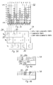
- Figure 3B illustrates a simple movable mirror device array 14 which includes 3 rows (labeled R A , R B and R C ) by 4 columns of mirror elements 28.
- Figure 3A represents the object 32 to be illuminated where each of the boxes 38 is one pixel. In printing applications, this object 32 may be a rotating printer drum (e.g., element 26 in Figure 1A) which will transfer toner to a sheet of paper (element 27 in Figure 1A).
- the first row R A of movable mirror device 14 will print the pixels under the columns labeled C A (i.e., columns 1, 4, 7, etc.) in Figure 3A, while the second row R B will print the pixels under the columns labeled C B and the third row R C will print the pixels under the columns labeled C C .
- the resulting line of imagery corresponds to that illustrated in Figure 2B.
- the first, fourth, seventh, etc. (columns C A ) of line 1 of object 32 will be selectively illuminated by light from the illuminated portions 30 of the first row R A of mirror elements 28.
- the areas on object 32 which may be illuminated are labeled t 1 .
- the box will have shifted down such that line 2 of the object is illuminated by light from the first row R A of mirror elements 28.
- the first, fourth, seventh, etc. columns C A of line 3 of the object can be illuminated by the light reflected from mirror elements 28 in the first row R 1 of movable mirror device 14.
- the first and second lines are not illuminated since they are now aligned with the upper non-illuminated portion of the second row R B and the lower non-illuminated portion of the first row R A of mirror elements 28, respectively.
- both line 1 and line 4 are simultaneously printed as illustrated by the pixels labeled t 4 in Figure 3A.
- the first, fourth, seventh, etc. (columns C A ) of line 4 are illuminated by light reflected from mirror elements 28 from the first row R A of movable mirror device 14.
- line 1 is now aligned with light from the second row R B of mirror elements 28.
- the second, fifth, eight, etc. (columns C B ) of this line can be illuminated.
- the second and third lines are not illuminated since they are now aligned with the upper non-illuminated portion of the second row R B and the lower non-illuminated portion of the first row R A of mirror elements 28, respectively.
- the first line is aligned with the third row R C of mirror elements 28 so that portions of three lines (e.g., lines 1, 4, and 7 at time t 7 ) are being simultaneously illuminated. This shifting will continue until each of the lines of object 32 have been selectively illuminated.
- FIGS 3C and 3D can be utilized to demonstrate a scanned system as illustrated in Figure 1A or 1B.
- each row R A , R B , or R C is illuminated at a different time by a beam which is as long as the movable mirror device and whose height is equal to that of the illuminated portion of the mirror element on the movable mirror device. Accordingly, at time t 1 line 1 is illuminated.
- time t 2 and t 3 no part of object 32 is illuminated since no part is aligned with the array 14.
- line 1 of the object 32 is aligned with the second row R B of spatial light modulator 14. This sequence will continue until each pixel 38 is imaged.
- the light illuminates the apertures for only one third of the time that the beam is scanned over the movable mirror device.
- This inefficiency is made up for because the light source can be turned on only when the scanner is pointed to the aperture over each mirror element 28. Hence, the light source can be turned on only when the scanner is pointed to the aperture over the mirror element.
- one third of the light transmitted will reach the movable mirror device (as illustrated by the fact that the illuminated portion 30 extends one third of each mirror element).
- Figures 4A and 4B illustrate two alternate embodiments of movable mirror device 14 arrays. These embodiments are similar to those previously discussed with respect to Figures 2A (and 3B and 3D).
- the mirror elements 28 are disposed in aligned columns.
- the illuminated portions 30 are staggered such that the illuminated portion 30A in row 1 of Figure 4A is aligned to the left edge of mirror element 28A while the illuminated portion 30B is centered in mirror element 28B and illuminated area 30C is aligned to the right edge of mirror element 28C.
- the same results as illustrated by Figures 3A and 3B (or 3C and 3D) may be achieved. It is also noted that the illuminated portions 30 do not need to be centered in the staggered array ( Figure 2A).
- Figure 4B has been included to illustrate the fact that the illuminated portions 30 are not required to be square.
- the illuminated portions comprise rectangular areas 30 on each mirror element 28.
- the resulting pixel elements which will be printed will be rectangular in this case. While square pixel elements are typically preferred, it is noted that other shaped elements such as rectangles, circles, triangles and other polygons may also be used. Of course, if isomorphic optics are used, the rectangular portion of the mirror element can be used to create a square image.
- the controlled illumination can be obtained by object plane or image plane illumination as depicted in Figures 5, 6, 7A and 7B.
- image plane illumination a mask 34 (shown in Figure 6 as well) containing apertures is illuminated by illumination source 12 and imaged by a lens 36 onto the movable mirror device 14 as shown in Figure 5.
- the apertures 38 may comprise square apertures as well as other shaped apertures.
- the mask 34 in object plane illumination the mask 34 is placed very close to the movable mirror device 14. Effectively, the movable mirror device 14 is in the object plane of the mask 34. Object plane illumination may typically be preferred since there is no intervening lens 34 to introduce distortions. Also, the resulting system is smaller. The smaller structure is easier to make rigid. As illustrated in Figure 7B, the mask 34 should be close to the movable mirror device 14 so that the beam falling on the movable mirror device mirror element 28 ( Figure 2A) is about the same size as the mask 34 aperture 38 ( Figure 6). Calculations indicate that a distance of less than about 10 microns, for example about 3 to 6 microns, should suffice. If the beam defracts so much that the entire mirror element 28 is illuminated, a large fraction of the light reflected back from the mirror 28 will not exit the aperture 38 and pass through the remainder of the optics.
- the movable mirror device 14 is imaged onto the drum 26 as illustrated in Figures 1A-D. Since the drum is rotating, the exposure should be short in time so the charge generated on the drum is not "smeared” resulting in the loss of image in the direction of motion of the drum.
- the short exposure can be obtained by driving the light source with a pulsed waveform. Typical waveforms have a pulsed duration of 33 microseconds with a 10% duty cycle. A 10% duty cycle is maybe inefficient in terms of light output since the source is off 90% of the time.
- a efficient approach is to leave the light source 12 on continuously and scan the beam over the mask 34 at such a speed that the aperture is illuminated for only a short time, for example 33 microseconds.
- the light source 12 can be operated at a 33% duty cycle without loss and efficiency.
- the source can be pulsed as described so long as the scanned beam illuminates only a single row of mirrors at a given instant.
- the use of coherent illumination of the movable mirror device has resulted in spurious and offensive diffraction patterns from the movable mirror device hinges and mirror elements.
- the location of the mask 34 controls the portion if the movable mirror device 14 which is illuminated.
- the mask can be positioned so that only the desired portion 30 of the mirror element 28 is illuminated.
- the concept of a mask offers an alternative means of manufacturing movable mirror device's.
- the movable mirror device 14 need not be designed so that the mirror element 28 is of optical quality throughout all portions of the mirror element. This design tolerance is possible since the portions of the mirror element 28 which are not of optical quality can be covered with the mask 34.
- the mask 34 also allows the size of the mirror elements 28 to be effectively changed without actually changing the physical dimension of the elements.
- a standard movable mirror device 14 can be built with a single mirror size and effective size of the mirror set by the size of the mask aperture 38.
- FIG 8A An alternate embodiment spatial light modulator array 14 is illustrated in Figure 8A.
- a smaller mirror element 28 is included.
- the smaller mirror element 28 covers only a portion of the area of the larger mirror elements 28 (as in Figure 2A).
- the mirror element 28 has a length and width which is one half of the full coverage mirrors (as in Figure 2A). Accordingly, two rows R A and R B are utilized to image each line of text. A representation of the text line is illustrated in Figure 8B.
- the micromirrors 28 shown in Figure 8A are shaded and cross-hatched. This pattern is repeated along the movable mirror device in the process dimension.
- the micromirrors 28 may be on about 17 micron centers and may be about 8 microns on the side.
- the pixels may be square and, for example, about 42 microns on the side.
- the shaded micromirrors 28 (in Figure 8A) expose the shaded pixels (in Figure 8B) and the cross-hatch micromirrors 28 expose the cross-hatch pixels.
- the array 14 is 2.4 inches long and 2.18 mm high and may be magnified by a factor of 5 on the drum. This version has 600 dpi (dots per inch) performance.
- the array is 4.8 inches by 2.18 mm and is magnified by a factor of 2.5 to the movable mirror device. This embodiment has 1200 dpi performance.
- the spatial light modulator array 14 can be used in either a scanned system ( Figure 1B) or a staring system ( Figure 1A).
- the mirror elements 28 are diamond shaped.
- diamond shaped mirror elements 28 include any mirror elements which are rotated such that non-parallel edges of adjacent mirror elements are next to each other.
- the mirror elements 28 are square but other shapes may also be utilized.
- the mirror elements 28 may be 11.3 microns long on the side and spaced on 17 micron centers.
- This architecture if used directly, will produce pixels as shown in Figure 9B. Note that the imaged pixels are non-contiguous. The non-exposed region is not the shape of the micromirrors and cannot be exposed by them for contiguous coverage as was possible with the systems of Figures 1A-D.
- the discontinuities of coverage can be eliminated.
- the first row R A of mirror elements will image the pixels labeled C A in Figure 9C.
- the object 32 will then shift (e.g. the drum 26 will rotate) and the second row R B of mirror elements will image the pixels labeled C B .
- the scanned mode will continue alternating between the first row R A until the entire page has been written to.
- Figure 10A Another embodiment architecture for the movable mirror device 14 is shown in Figure 10A.
- the upper portion of Figure 10A shows a first sub-array 14a of three rows of micromirrors 28 which are shaded.
- these micromirrors 28 may be on about 17 micron centers and diamond shaped with sides which may be about 11.3 microns.
- a second and identical sub-array 14b is shown below sub-array 14a.
- this sub-array 14b may be displaced by 8.5 microns in the vertical (or process) direction and displaced by 8.5 microns in the horizontal (or cross-process) direction. That sub-array pattern may be repeated in the process direction providing as many micromirrors as needed.
- Figure 10A shows three micromirror rows per sub-array 14a and 14b. However, there could be more. The limit is determined by the registration requirements of the micromirror images in successive exposures. While specific dimensions are provided as examples, it is noted that any appropriate size micromirror may be used.
- Figure 10B depicts the pixels written on the drum 26 ( Figure 1B) by a movable mirror device 14 of this configuration.
- One set of cross-hatched pixels 38a are written by the upper subarray 14a and another set of cross-hatched pixels 38b are written by the lower sub-array 14b. Note that contiguous coverage of pixels is obtained on the object 32 by this architecture.
- Each row in subarrays 14a and 14b can be utilized to image a separate line, or alternatively, each row can be used to image the same line a number of times. Multiple imaging may be desired if enough light energy cannot be transmitted to the object to be illuminated in a single illumination period. It is further noted that the multiple imaging rows can also be utilized in any of the other embodiments described herein (e.g., the embodiment of Figures 2A, 3A or 3B, 4A, 4B, or 8A).
- the movable mirror device array of Figure 10A may be utilized in a number of ways.
- a movable mirror device which is 4.8 inches by 1.08 mm may be magnified by a factor of 2.5.
- the resulting performance is 900 dpi in the 45 degree direction of the copy and is 600 dpi in the process dimension.
- a movable mirror device 14 of this architecture may be 3.4 in long and 1.08 mm high.
- the movable mirror device 14 is magnified by a factor of 3.4 and has 600 dpi performance is the 45 degree direction.
- Figure 11 shows an alternative approach to using isomorphic optics.
- the movable mirror device 814 has twice as many elements in the horizontal or cross-production cross-process direction as the movable mirror device 14 in Figure 1A. Also the magnification is reduced by a factor of two to maintain the same page width as in Figure 1A. The resulting four phases are illustrated in Figure 12.
- Each pixel 40 has four non-overlapping phases labeled 1, 2, 3, and 4 in Figure 12. (The pixel 40 is equivalent to each pixel 38 in the array illustrated in Figure 3A.) Since each pixel 40 is so small, the human eye cannot differentiate the four phases but can only add them together. Therefore, if a really dark pixel is desired, each of the subphases 1, 2, 3, and 4 will be printed to. On the other hand, as a less dark pixel is desired, only some of the subphases 1, 2, 3, or 4 will be illuminated.
- FIGs 13 and 14 illustrate two light sources 12 which may be utilized with the present invention.
- Most proposed LEDs for the printer applications consist of widely spaced discrete LED emitting areas as shown in Figure 13. This light source may also be used with the embodiments described with respect to the present invention.
- FIG 14 illustrates an LED array which may be used with the present invention.
- An LED array is a high power LED which permits several improvements in the printing system.
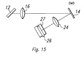
- the LED array has emitting areas placed as close to each other as feasible and forms, to the extent possible, a continuum of emitting areas as depicted in Figure 14. Since the shape of the movable mirror device array of 14 is a long and narrow rectangle, the LED is also long and narrow so that a relatively simple isometric imaging system can be used to relay the light to the movable mirror device 14 as illustrated in Figure 15.
- the additional power provided by the "super LED” can be invested in several ways to lower the cost and size of the system.
- the f-number of lens 24 in Figure 15 can be increased since more light is available by reducing their diameter.
- the f-number can be increased so long as the resolution of lens 24 is sufficient to produce a sharp enough pixel on the drum. The result will be a greater depth of field in the plane of the drum 26 allowing the drum 26 to wobble more during its rotation and generally loosening the tolerances to which it must be position.
- the additional power provided by the LED array could also allow lower transmission lens elements 16 and 24 to be used and still maintain adequate exposure.
- Current designs require up to 30 or more exposures by movable mirror device elements to achieve maximum density on the copy.
- a more powerful LED would allow a maximum exposure with fewer movable mirror device elements reducing the cost of the movable mirror device.
- the LED array also permits the use of the mask approach to controlling the illumination on the movable mirror device for the staggered array concept as discussed previously.
- the biggest objection to the mask is the loss of energy caused by the presence of the mask 34.
- the opaque area of the mask 34 can cause a loss of 90% or more of the light from the LED 12. However, the increased light from the LED array could offset this loss.
- the width of the movable mirror device 14 array could be reduced by a factor of three. If the same F # is maintained to preserve the exposure energy, the diameter and focal lengths of the lenses 16 and 24 of Figure 15 can be reduced by a roughly factor of three. Such reduction would reduce the cost and volume of the optics. The width of the movable mirror device 14 would also be reduced by a factor of three resulting in the substantially smaller movable mirror device 14 although the number of mirrored elements would remain unchanged.
- the width of the staggered movable mirror device array could be doubled with the attendant doubling the number of mirror elements.
- the movable mirror device array would now be two-thirds the original size rather than one-third the size.
- the writing algorithm depicted in Figure 12 could now be used providing a rectangular writing spot with an isomorphic optical system.
Abstract
A system (10) for independently illuminating a plurality of areas on an object (26) such as a printer drum is disclosed herein. The system 10 includes a light source (12) such as an LED or a plurality of LEDs. A spatial light modulator (14), which may be a movable mirror device, receives light from the light source (12) and reflects selected portions of the light. The spatial light modulator (14) includes at least n rows of independently modulated pixels wherein only 1/nth of each of the rows can receive and reflect light at any point in time. The light from the spatial light modulator (14) is imaged (e.g., with imaging lens (24) onto rows and columns of the object (26) to be illuminated. The object (26) is illuminated in such a way that each column is illuminated by a corresponding row of pixels.
Description
- The following patents are hereby incorporated herein by reference:
Patent No.File Date Issue Date TI Case No.
5,061,049 09/13/90 10/29/91 TI-13173B
5,083,857 06/29/90 01/28/92 TI-14568
5,101,236 12/21/89 03/31/92 TI-14585
5,172,161 12/31/90 12/15/92 TI-15602
5,430,524 03/28/94 07/04/95 TI-15602AC - This invention generally relates to display and printer systems and specifically to a printing system which uses a staggered array spatial light modulator.
- The requirement for hardcopy output is a ubiquitous element of the information revolution. In particular, electrophotography has become one of the most widely used systems and the dry toner process, has become the most popular for creating copies and prints of documents in a host of environments. The basics of electrophotography are well know to those skilled in the art. The fundamental elements of a electrophotographic printer or copier using the dry toner process include a photo sensitive medium, typically an organic photoreceptor (OPC), which is charged electrostatically to a predetermined voltage and polarity. Upon exposure to an optical image, generated by reflection or a light modulating system, portions of the originally uniform electrostatic charge on the OPC are erased where illuminated. Thus, an electrostatic latent image of the original (or the electronic) document is created on the OPC. In most modern systems, this image is passed by a source of developer materials which consists of electrostatically charged toner particles held to ferromagnetic carrier beads. The carriers are used to facilitate the transport of the materials into contact with the above mentioned latent image through the action of magnetic fields and rotating magnets within sleeved cylinders, typically called developer rollers. Through a designed interplay of electrostatic charges, the toner particles that are typically in the 10 micron diameter range, are separated from the carrier beads, typically 50 micron diameter particles, and retained in-place on the appropriate portions of the latent image resident on the OPC surface. The magnetic forces associated with the developer rollers carry the depleted ferromagnetic carrier beads back to the position where they are re-mixed with additional toner for development of subsequent images.
- As is well known, the toner materials are normally plastics with flow promoting agents, charge control agents, and color pigments which melt at a predetermined temperature. The OPC surface then carries a developed latent image after exiting the proximity of the developing roller. Subsequently, the photoreceptor surface carrying the developed image is brought into contact with an image receptor, which in most common applications of electrophotography is a sheet of paper, but may be an intermediate material suitable for the build-up of multiple pigmented images as required for color printing. Electrostatic charging systems are typically used to transfer the toner from the OPC to the image receptor.
- Whether the final image bearing member is ultimately paper or an other material, it can be successively operated on by multiple photoreceptors, a single photoreceptor, or an image bearing intermediate member to build up the full color image. It exits the printing process through a station referred to as the fuser, where the appropriate heat and/or pressure is applied to the image receptor and thereby fixes the image permanently.
- One technology which has been found to be useful in printing and display applications utilizes a movable mirror device such as the Digital Micromirror Device (also referred to as Deformable Mirror Device or simply a DMD) manufactured by Texas Instruments, Inc. The movable mirror device is composed of many small mirrors called micromirrors which rotate about a fixed axis. The movable mirror device is illuminated with a beam of light. The rotation of the micromirror causes the light illuminating the micromirror to be deflected under the control of the rotation. Thus, each micromirror of a movable mirror device can be selectively rotated thereby patterning light reflected from the array. Specific details of movable mirror devices are provided in US Patent No. 5,061,049 and 5,083,857, each of which is incorporated herein by reference.
- When using a movable mirror device in print applications, a long and narrow movable mirror device will typically be used. As an example, a movable mirror device array with about 100 rows and 7,000 columns may be utilized. To produce a device of this size, the chip may typically be 5.0 inches long.
- A system for independently illuminating a plurality of areas on an object, such as a printer drum, is disclosed herein. The system includes a light source, such as a single light emitting diode (LED) or a plurality of LEDs. A spatial light modulator, which may be a movable mirror device, such as the Digital Micromirror Device (DMD) manufactured by Texas Instruments, Inc., receives light from the light source and reflects selected portions of the light. In some embodiments the mirror device is illuminated in a scanning mode, i. e., each row of mirror elements is illuminated individually and sequentially by scanning a beam of light over all of the micromirrors. In other embodiments, the mirror device is illuminated in a staring mode, i.e., all the mirror elements of the entire array are illuminated simultaneously. The light from the spatial light modulator is imaged onto the object to be illuminated which is partitioned into rows of pixels (picture elements). The object is illuminated in such a way that each pixel is, over time, illuminated by light from a corresponding column of micromirrors.
- An advantage of the invention is that it reduces the number of columns of micromirrors required by the movable mirror device. This reduction may be important in printing applications where the number of columns is very high resulting in physically large integrated circuit chips which are difficult to illuminate. The reduction in the size of the chip will reduce the cost to manufacture the chip as well as the cost of the optical subsystem to illuminate the chip thereby reducing the cost of the system which the chip subsequently is installed.
- The above features of the present invention will be more clearly understood from consideration of the following descriptions in connection with accompanying drawings in which:
- Figure 1A is a block diagram of a first scanning mode embodiment printing system;
- Figure 1B is a block diagram of a detailed view of the first scanning mode embodiment printing system shown in Figure 1A;
- Figure 1C is a block diagram of a staring mode embodiment printing system;
- Figure 1D is a block diagram of a second scanning mode embodiment printing system;
- Figure 2A is a block diagram of a movable mirror device array illustrating the portion of each micro-mirror element which is illuminated;
- Figure 2B illustrates a representation of the line which will eventually be printed;
- Figures 3A and 3B illustrate an object (such as an OPC) to be illuminated as well as a movable mirror device to provide the illumination in accordance with a staring mode;
- Figures 3C and 3D illustrate an object (such as an OPC) to be illuminated as well as a movable mirror device to provide the illumination in accordance with a scanning mode;
- Figures 4A and 4B illustrate alternative movable mirror device arrays;
- Figure 5 illustrates an image plane application for illuminating the movable mirror device;
- Figure 6 illustrates a mask which is utilized to control the illumination of the movable mirror device;
- Figures 7A and 7B illustrate an object plane implementation of illuminating the movable mirror device array;
- Figures 8A, 9A, and 10A are block diagrams of alternative embodiments of movable mirror device arrays;
- Figures 8B, 9B-C and 10B are representations of the line which will be written by the array of the corresponding Figure 8A, 9A, or 10A;
- Figure 11 is a schematic of a second embodiment printing system;
- Figure 12 illustrates a gray level algorithm for an alternative system which using isomorphic optics;
- Figure 13 illustrates an LED array which may be utilized by the systems of the present invention;
- Figure 14 illustrates an LED array which may be utilized by the system of the present invention; and
- Figure 15 is a schematic of a system utilizing an LED array.
- A first embodiment of the staggered
array printing system 10 is of the scan mode variety and is depicted in Figure 1A. Alight source 12, such as a light laser diode, illuminates a spatiallight modulator 14. The spatiallight modulator 14 may comprise a movable mirror device such as the Digital Micromirror Device (DMD) manufactured by Texas Instruments and described in US Patents 5,061,049 and 5,083,857, incorporated herein by reference. - In the system of Figure 1A, the light from the
light source 12 is scanned over the movable mirror device by means oflight scanning optics 13. The light illuminating the movable mirror device from thelight source 12 forms a long and narrow beam on the movable mirror device. The length of the beam is equal to the length of the movable mirror device array and the width of the beam is equal to the width of the illuminated portion of micromirrors. In the preferred embodiment, each row of micromirrors of the movable mirror device array is sequentially illuminated. In the scanned mode, the beam is scanned rapidly enough that all of the mirror elements are illuminated during a time interval short enough that the illuminated object, such as aprinter drum 26, turns only a small fraction of a pixel. - Modulated light is reflected from the spatial
light modulator 14 intoprojection lens 24 which images the light onto thedrum 26. Thelens 24 may be an anamorphic lens if it is desired to have a printing beam which is not the same shape as the micromirror. Therotating drum 26 may then transfer toner to a sheet ofpaper 27. - In the embodiment illustrated in Figure 1B, the
light scanning optics 13 comprises afirst lens 18, ascanner 20, and athird lens 22. Thescanner 20 scans the light beam down the array within the spatiallight modulator 14 in the vertical direction successively illuminating the movable mirror device mirror elements in each row. - Figure 1C depicts a staring mode embodiment of the staggered
array printing system 10. Thelight source 12, such as a light emitting diode (LED), illuminates the spatiallight modulator 14. As in the embodiments of Figures 1A and 1B, the spatiallight modulator 14 may comprise a movable mirror device such as the Digital Micromirror Device (DMD) manufactured by Texas Instruments and described in US Patents 5,061,049 and 5,083,857. - In the system of Figure 1C, the light from the
light source 12 is directed toward the movable mirror device by means of light directingoptics 16. The light beam illuminates all of the micromirrors of the moving mirror device simultaneously. Modulated light is reflected from the spatiallight modulator 14 into theprojection lens 24 which images the light onto thedrum 26. - In the preferred embodiment, the
light source 12 is pulsed (rapidly turned on and then off) at a period equal to that required by thedrum 26 to rotate through one pixel. The light pulse will preferably have a 10% duty cycle so that a sharp image of the mirror element is formed on the drum 26 (i.e., the mirror element image is not "smeared" by the rotation of the drum). Thelens 24 may be an anamorphic lens if it is desired to have a printing beam which is not the same shape as the micromirror. Therotating drum 26 may then transfer toner to the sheet ofpaper 27. - In Figure 1D, the
light source 12 is a linear array of LED emitters and thelight directing optics 16 is a toroidal lens which magnifies the LED emitters so that the image of each emitter fills the DMD. - A first embodiment of the spatial
light modulator 14 for the embodiments of Figures 1A-D is illustrated in the simplified version in Figure 2A. The spatiallight modulator 14 preferably comprises a movable mirror device such as the Digital Micromirror Device (DMD) manufactured by Texas Instruments, Inc. - This
movable mirror device 14 is configured in a plurality of rows and columns as illustrated in Figure 2A. Each of the rows comprises a plurality of mirror elements (sometimes called micromirrors) 28. In the embodiment illustrated here, each row ofmirror elements 28 is displaced in the horizontal direction by 1/3 of a mirror dimension. Each of the three rows will illuminate 1/3 of the object to be illuminated, e.g., thedrum 26 as shown in Figures 1A-D. While illustrated herein with three rows each shifted a 1/3 of a mirror dimension, it should be noted that any number of rows larger than one may be used. In general, if n-rows are used each mirror will be displaced in the horizontal direction by 1/nth of a mirror dimension. - In the embodiment illustrated in Figure 2A only the
center 30 of eachmirror element 28 is illuminated. In this case, the area of eachmirror element 28 illuminated is a square whose dimension on each edge is 1/3 of the length of the movable mirrordevice mirror element 28. Of course, if the number of rows in a set of rows is different than three, then the dimension of the illuminated portion is different. - The first row will print the pixels labeled 1 in Figure 2B, the second row will print the pixels labeled 2 in Figure 2B and the third row will print the pixels labeled 3 in Figure 2B. Since three rows of
movable mirror device 14 are used to print a single line, themovable mirror device 14 can be built with only 1/3 of the total columns. This decrease in the number of columns provides a significant manufacturability advantage over the prior art. - The operation of a staring system embodiment (e.g., as illustrated in Figures 1C and 1D) will now be described with reference to Figures 3A and 3B. Figure 3B illustrates a simple movable
mirror device array 14 which includes 3 rows (labeled RA, RB and RC) by 4 columns ofmirror elements 28. Figure 3A represents theobject 32 to be illuminated where each of theboxes 38 is one pixel. In printing applications, thisobject 32 may be a rotating printer drum (e.g.,element 26 in Figure 1A) which will transfer toner to a sheet of paper (element 27 in Figure 1A). The first row RA ofmovable mirror device 14 will print the pixels under the columns labeled CA (i.e.,columns - To understand how the pixels are printed, imagine the box of Figure 3A being slid down the page over the movable mirror device array of Figure 3B. In the known electrophotographic (i.e., xerographic) printing process, this movement occurs when the drum 26 (Figure 1A) rotates such that different portions of the
drum 26 are in the light path of the beam reflected frommovable mirror device 14. To print, toner (not shown) is applied to thedrum 26 surface and adheres to the spots where the modulated light impacts the drum. This toner, in turn, is transferred to a piece of paper (27 in Figure 1A) which is moved adjacent to thedrum 26. For a more detailed description of a light energy management system which can be used with a xerographic reproduction system, reference should be made to U.S. Patent 5,101,236, incorporated herein by reference. - Returning to Figures 3A and 3B, at a first time t1 the first, fourth, seventh, etc. (columns CA ) of
line 1 ofobject 32 will be selectively illuminated by light from the illuminatedportions 30 of the first row RA ofmirror elements 28. The areas onobject 32 which may be illuminated are labeled t1. At a second time t2, the box will have shifted down such thatline 2 of the object is illuminated by light from the first row RA ofmirror elements 28. - At time t2, nothing can be written to
line 1 since this line will now be aligned to the lower non-illuminated portion of first row RA ofmirror elements 28. - Similarly, at a third time t3 the first, fourth, seventh, etc. columns CA of
line 3 of the object can be illuminated by the light reflected frommirror elements 28 in the first row R1 ofmovable mirror device 14. Once again, the first and second lines are not illuminated since they are now aligned with the upper non-illuminated portion of the second row RB and the lower non-illuminated portion of the first row RA ofmirror elements 28, respectively. - At a fourth time t4 both
line 1 andline 4 are simultaneously printed as illustrated by the pixels labeled t4 in Figure 3A. The first, fourth, seventh, etc. (columns CA) ofline 4 are illuminated by light reflected frommirror elements 28 from the first row RA ofmovable mirror device 14. At the same time,line 1 is now aligned with light from the second row RB ofmirror elements 28. Accordingly, the second, fifth, eight, etc. (columns CB) of this line can be illuminated. Note that during the fourth time t4, the second and third lines are not illuminated since they are now aligned with the upper non-illuminated portion of the second row RB and the lower non-illuminated portion of the first row RA ofmirror elements 28, respectively. - At time t7 the first line is aligned with the third row RC of
mirror elements 28 so that portions of three lines (e.g.,lines object 32 have been selectively illuminated. - Figures 3C and 3D can be utilized to demonstrate a scanned system as illustrated in Figure 1A or 1B. In the scanned system, each row RA, RB, or RC is illuminated at a different time by a beam which is as long as the movable mirror device and whose height is equal to that of the illuminated portion of the mirror element on the movable mirror device. Accordingly, at time t1 line 1 is illuminated. During times t2 and t3, no part of
object 32 is illuminated since no part is aligned with thearray 14. Note that at time t11,line 1 of theobject 32 is aligned with the second row RB of spatiallight modulator 14. This sequence will continue until eachpixel 38 is imaged. - It is, of course, noted that in the scanning mode the light illuminates the apertures for only one third of the time that the beam is scanned over the movable mirror device. This inefficiency, however, is made up for because the light source can be turned on only when the scanner is pointed to the aperture over each
mirror element 28. Hence, the light source can be turned on only when the scanner is pointed to the aperture over the mirror element. In addition, during the scanned mode one third of the light transmitted will reach the movable mirror device (as illustrated by the fact that the illuminatedportion 30 extends one third of each mirror element). In the staring mode in which the entire movable mirror device is illuminated, only one-ninth of the light reaches the movable mirror device since the area occupied by the apertures over the mirror elements account for only one ninth of the area of the movable mirror device. - Figures 4A and 4B illustrate two alternate embodiments of
movable mirror device 14 arrays. These embodiments are similar to those previously discussed with respect to Figures 2A (and 3B and 3D). In the embodiment in Figure 4A, themirror elements 28 are disposed in aligned columns. In this case, theilluminated portions 30 are staggered such that the illuminated portion 30A inrow 1 of Figure 4A is aligned to the left edge of mirror element 28A while the illuminated portion 30B is centered in mirror element 28B and illuminated area 30C is aligned to the right edge of mirror element 28C. Using this technique, the same results as illustrated by Figures 3A and 3B (or 3C and 3D) may be achieved. It is also noted that theilluminated portions 30 do not need to be centered in the staggered array (Figure 2A). - Figure 4B has been included to illustrate the fact that the
illuminated portions 30 are not required to be square. In this example, the illuminated portions compriserectangular areas 30 on eachmirror element 28. The resulting pixel elements which will be printed will be rectangular in this case. While square pixel elements are typically preferred, it is noted that other shaped elements such as rectangles, circles, triangles and other polygons may also be used. Of course, if isomorphic optics are used, the rectangular portion of the mirror element can be used to create a square image. - The controlled illumination can be obtained by object plane or image plane illumination as depicted in Figures 5, 6, 7A and 7B. In image plane illumination, a mask 34 (shown in Figure 6 as well) containing apertures is illuminated by
illumination source 12 and imaged by alens 36 onto themovable mirror device 14 as shown in Figure 5. Theapertures 38 may comprise square apertures as well as other shaped apertures. - Alternatively, as illustrated in Figure 7A, in object plane illumination the
mask 34 is placed very close to themovable mirror device 14. Effectively, themovable mirror device 14 is in the object plane of themask 34. Object plane illumination may typically be preferred since there is no interveninglens 34 to introduce distortions. Also, the resulting system is smaller. The smaller structure is easier to make rigid. As illustrated in Figure 7B, themask 34 should be close to themovable mirror device 14 so that the beam falling on the movable mirror device mirror element 28 (Figure 2A) is about the same size as themask 34 aperture 38 (Figure 6). Calculations indicate that a distance of less than about 10 microns, for example about 3 to 6 microns, should suffice. If the beam defracts so much that theentire mirror element 28 is illuminated, a large fraction of the light reflected back from themirror 28 will not exit theaperture 38 and pass through the remainder of the optics. - The
movable mirror device 14 is imaged onto thedrum 26 as illustrated in Figures 1A-D. Since the drum is rotating, the exposure should be short in time so the charge generated on the drum is not "smeared" resulting in the loss of image in the direction of motion of the drum. The short exposure can be obtained by driving the light source with a pulsed waveform. Typical waveforms have a pulsed duration of 33 microseconds with a 10% duty cycle. A 10% duty cycle is maybe inefficient in terms of light output since the source is off 90% of the time. A efficient approach is to leave thelight source 12 on continuously and scan the beam over themask 34 at such a speed that the aperture is illuminated for only a short time, for example 33 microseconds. Since theapertures 38 are spaced at a different distance apart equal to three times their dimension, thelight source 12 can be operated at a 33% duty cycle without loss and efficiency. The source can be pulsed as described so long as the scanned beam illuminates only a single row of mirrors at a given instant. - In other movable mirror device applications, the use of coherent illumination of the movable mirror device has resulted in spurious and offensive diffraction patterns from the movable mirror device hinges and mirror elements. There should be not such scattering problem here since the location of the
mask 34 controls the portion if themovable mirror device 14 which is illuminated. The mask can be positioned so that only the desiredportion 30 of themirror element 28 is illuminated. - The concept of a mask offers an alternative means of manufacturing movable mirror device's. The
movable mirror device 14 need not be designed so that themirror element 28 is of optical quality throughout all portions of the mirror element. This design tolerance is possible since the portions of themirror element 28 which are not of optical quality can be covered with themask 34. Themask 34 also allows the size of themirror elements 28 to be effectively changed without actually changing the physical dimension of the elements. A standardmovable mirror device 14 can be built with a single mirror size and effective size of the mirror set by the size of themask aperture 38. - An alternate embodiment spatial
light modulator array 14 is illustrated in Figure 8A. In this embodiment, asmaller mirror element 28 is included. Thesmaller mirror element 28 covers only a portion of the area of the larger mirror elements 28 (as in Figure 2A). In the example illustrated in Figure 8A, themirror element 28 has a length and width which is one half of the full coverage mirrors (as in Figure 2A). Accordingly, two rows RA and RB are utilized to image each line of text. A representation of the text line is illustrated in Figure 8B. - The
micromirrors 28 shown in Figure 8A are shaded and cross-hatched. This pattern is repeated along the movable mirror device in the process dimension. As an example, themicromirrors 28 may be on about 17 micron centers and may be about 8 microns on the side. As before, the pixels may be square and, for example, about 42 microns on the side. The shaded micromirrors 28 (in Figure 8A) expose the shaded pixels (in Figure 8B) and thecross-hatch micromirrors 28 expose the cross-hatch pixels. In one possible embodiment, thearray 14 is 2.4 inches long and 2.18 mm high and may be magnified by a factor of 5 on the drum. This version has 600 dpi (dots per inch) performance. In a second embodiment, the array is 4.8 inches by 2.18 mm and is magnified by a factor of 2.5 to the movable mirror device. This embodiment has 1200 dpi performance. - The operation of the embodiment shown in Figure 8A is analogous to the operation of the previously described systems. This embodiment provides the advantage of eliminating the necessity of
mask 34 of Figures 5, 6, 7A and 7B. As with the other embodiments, the spatiallight modulator array 14 can be used in either a scanned system (Figure 1B) or a staring system (Figure 1A). - An alternate architecture of the
movable mirror device 14 is shown in Figure 9A. Themirror elements 28 are diamond shaped. In this context, diamond shapedmirror elements 28 include any mirror elements which are rotated such that non-parallel edges of adjacent mirror elements are next to each other. In the illustrated example, themirror elements 28 are square but other shapes may also be utilized. For example, themirror elements 28 may be 11.3 microns long on the side and spaced on 17 micron centers. This architecture, if used directly, will produce pixels as shown in Figure 9B. Note that the imaged pixels are non-contiguous. The non-exposed region is not the shape of the micromirrors and cannot be exposed by them for contiguous coverage as was possible with the systems of Figures 1A-D. - However, if the array shown in Figure 9A is utilized with a scanned system as illustrated in Figure 1B, the discontinuities of coverage can be eliminated. In this embodiment, the first row RA of mirror elements will image the pixels labeled CA in Figure 9C. The
object 32 will then shift (e.g. thedrum 26 will rotate) and the second row RB of mirror elements will image the pixels labeled CB. The scanned mode will continue alternating between the first row RA until the entire page has been written to. - Another embodiment architecture for the
movable mirror device 14 is shown in Figure 10A. The upper portion of Figure 10A shows a first sub-array 14a of three rows ofmicromirrors 28 which are shaded. As an example, thesemicromirrors 28 may be on about 17 micron centers and diamond shaped with sides which may be about 11.3 microns. A second and identical sub-array 14b is shown belowsub-array 14a. In the given example, this sub-array 14b may be displaced by 8.5 microns in the vertical (or process) direction and displaced by 8.5 microns in the horizontal (or cross-process) direction. That sub-array pattern may be repeated in the process direction providing as many micromirrors as needed. Figure 10A shows three micromirror rows persub-array - Figure 10B depicts the pixels written on the drum 26 (Figure 1B) by a
movable mirror device 14 of this configuration. One set ofcross-hatched pixels 38a are written by theupper subarray 14a and another set ofcross-hatched pixels 38b are written by thelower sub-array 14b. Note that contiguous coverage of pixels is obtained on theobject 32 by this architecture. - Each row in
subarrays - The movable mirror device array of Figure 10A may be utilized in a number of ways. In one version a movable mirror device which is 4.8 inches by 1.08 mm may be magnified by a factor of 2.5. The resulting performance is 900 dpi in the 45 degree direction of the copy and is 600 dpi in the process dimension. In a second version a
movable mirror device 14 of this architecture may be 3.4 in long and 1.08 mm high. Themovable mirror device 14 is magnified by a factor of 3.4 and has 600 dpi performance is the 45 degree direction. - If a multiple phase printing algorithm is required, Figure 11 shows an alternative approach to using isomorphic optics. In Figure 11, the
movable mirror device 814 has twice as many elements in the horizontal or cross-production cross-process direction as themovable mirror device 14 in Figure 1A. Also the magnification is reduced by a factor of two to maintain the same page width as in Figure 1A. The resulting four phases are illustrated in Figure 12. - This embodiment can be used to provide increased gray level resolutions. Each
pixel 40 has four non-overlapping phases labeled 1, 2, 3, and 4 in Figure 12. (Thepixel 40 is equivalent to eachpixel 38 in the array illustrated in Figure 3A.) Since eachpixel 40 is so small, the human eye cannot differentiate the four phases but can only add them together. Therefore, if a really dark pixel is desired, each of thesubphases subphases - Figures 13 and 14 illustrate two
light sources 12 which may be utilized with the present invention. Most proposed LEDs for the printer applications consist of widely spaced discrete LED emitting areas as shown in Figure 13. This light source may also be used with the embodiments described with respect to the present invention. - Figure 14, on the other hand, illustrates an LED array which may be used with the present invention. An LED array is a high power LED which permits several improvements in the printing system. The LED array has emitting areas placed as close to each other as feasible and forms, to the extent possible, a continuum of emitting areas as depicted in Figure 14. Since the shape of the movable mirror device array of 14 is a long and narrow rectangle, the LED is also long and narrow so that a relatively simple isometric imaging system can be used to relay the light to the
movable mirror device 14 as illustrated in Figure 15. - The additional power provided by the "super LED" can be invested in several ways to lower the cost and size of the system. First of all, the f-number of
lens 24 in Figure 15 can be increased since more light is available by reducing their diameter. The f-number can be increased so long as the resolution oflens 24 is sufficient to produce a sharp enough pixel on the drum. The result will be a greater depth of field in the plane of thedrum 26 allowing thedrum 26 to wobble more during its rotation and generally loosening the tolerances to which it must be position. - The additional power provided by the LED array could also allow lower
transmission lens elements mask 34. The opaque area of themask 34 can cause a loss of 90% or more of the light from theLED 12. However, the increased light from the LED array could offset this loss. If the staggeredmovable mirror device 14 array uses three rows of movable mirrordevice mirror elements 28 to write each line, the width of themovable mirror device 14 array could be reduced by a factor of three. If the same F # is maintained to preserve the exposure energy, the diameter and focal lengths of thelenses movable mirror device 14 would also be reduced by a factor of three resulting in the substantially smallermovable mirror device 14 although the number of mirrored elements would remain unchanged. - If a rectangular writing spot is desired, the width of the staggered movable mirror device array could be doubled with the attendant doubling the number of mirror elements. The movable mirror device array would now be two-thirds the original size rather than one-third the size. However, the writing algorithm depicted in Figure 12 could now be used providing a rectangular writing spot with an isomorphic optical system.
Claims (20)
- A system for illuminating a plurality of areas on an object, said system comprising:a light source;a spatial light modulator for receiving light from said light source and reflecting selected portions of said light corresponding to said areas to be illuminated, said spatial light modulator comprising sets of n rows of pixels wherein only 1/n of said n rows may receive and reflect said light at any one point in time, wherein n is an integer greater than one; andsaid object to be illuminated by receiving said reflected light from said spatial light modulator, each of said areas being illuminated comprising p columns such that every nth one from a first of said P columns on said object is illuminated at said one point in time.
- The system of claim 1 wherein the illuminated portions of the n rows of pixels are staggered with respect to each other in a cross-process dimension so that one line of contiguous pixels can be written by successive exposures of each of the n rows to said light.
- The system of claim 2 wherein the spatial light modulator is composed of several subarrays of said n rows of pixels which are aligned so that each of said pixels can repeatedly be exposed on said object.
- The system of claim 3 wherein said spatial light modulator comprises a movable mirror device.
- The system of claim 4, wherein each of said pixels includes a deflectable beam, an address electrode adjacent said beam, and a landing electrode adjacent said beam;wherein a voltage applied between said beam and said address electrode deflects said beam toward said address electrode; andwherein said landing electrode is located to contact said beam deflected toward said address electrode and prevent said deflected beam from contacting said address electrode.
- The system of claim 5, wherein said pixels are formed in a layered structure;said layered structure including an insulated substrate, a spacer layer on said substrate, a conductive reflecting layer on said spacer layer, and a plurality of addressing and landing electrodes;each of said pixels including:a deflectable element formed in said reflecting layer and connected to the remainder of said reflecting layer by at least one hinge formed from said reflecting layer;a well formed in said spacer layer and extending from said deflectable element to said substrate,a first addressing electrode on said substrate at the bottom of said well and located to deflect said deflectable element by electrostatic attraction, anda first landing electrode on said substrate at the bottom of said well, said first landing electrode located both to contact said deflectable element when said deflectable element is deflected by attraction by said first addressing electrode to said substrate and to prevent said deflectable element from contacting said addressing electrode.
- The system of claim 6 wherein said pixels include diamond shaped mirror elements.
- The system of claim 7 wherein each of said mirror elements are smaller that spacing of said elements in each of said rows.
- The system of claim 8 wherein said light source is selected from the group consisting of a light emitting diode or laser diode or an incandescent lamp.
- The system of claim 9 wherein each of said sets includes three rows of said pixels.
- The system of claim 10 wherein said object comprises a printing drum.
- The system of claim 11 and further comprising a scanner positioned between said light source and said spatial light modulator, said scanner for imaging said light on some of said n rows of pixels.
- The system of claim 11 and further comprising light directing optics between said light source and said spatial light modulator for simultaneously illuminating all of said n rows of pixels.
- The system of any of claims 12-13, wherein only a portion of each of said pixels is illuminated.
- The system of claim 14 and further comprising a mask positioned between said light source and said spatial light modulator.
- The system of claim 15 wherein said mask is positioned less than 10 microns from said spatial light modulator.
- The system of claim 16 wherein only a square portion of each of said pixels is illuminated.
- The system of Claim 17 wherein each of said pixels is independently modulated.
- The system of Claim 18 wherein said object is a display device.
- A method of independently illuminating a plurality of areas on an object, said method comprising the steps of:transmitting light to a spatial light modulator;receiving said light at said spatial light modulator, said spatial light modulator comprising at least one set of n rows of independently modulated pixels wherein only 1/n of said rows may receive and reflect said light at any one point in time, wherein n is an integer greater than one;reflecting a modulated version of said light from said spatial light modulator toward said object to be illuminated; andreceiving said reflected light from said spatial light modulator at said object to be illuminated, said areas being illuminated comprising p columns such that each column on said object is illuminated by a corresponding row of said pixels.
Applications Claiming Priority (2)
| Application Number | Priority Date | Filing Date | Title |
|---|---|---|---|
| US424917 | 1995-04-19 | ||
| US08/424,917 US5754217A (en) | 1995-04-19 | 1995-04-19 | Printing system and method using a staggered array spatial light modulator having masked mirror elements |
Publications (2)
| Publication Number | Publication Date |
|---|---|
| EP0739125A2 true EP0739125A2 (en) | 1996-10-23 |
| EP0739125A3 EP0739125A3 (en) | 1999-03-10 |
Family
ID=23684425
Family Applications (1)
| Application Number | Title | Priority Date | Filing Date |
|---|---|---|---|
| EP96106193A Withdrawn EP0739125A3 (en) | 1995-04-19 | 1996-04-19 | Improvements relating to a display and printing system and method |
Country Status (7)
| Country | Link |
|---|---|
| US (1) | US5754217A (en) |
| EP (1) | EP0739125A3 (en) |
| JP (1) | JPH08318641A (en) |
| KR (1) | KR960038518A (en) |
| CN (1) | CN1140844A (en) |
| CA (1) | CA2174156A1 (en) |
| TW (1) | TW293116B (en) |
Cited By (5)
| Publication number | Priority date | Publication date | Assignee | Title |
|---|---|---|---|---|
| EP0873006A2 (en) * | 1997-04-18 | 1998-10-21 | MIVATEC Hard- und Software GmbH | Photoplotting method and apparatus for recording a computer-stored raster image on an even, light-sensitive recording medium |
| EP0931667A2 (en) * | 1998-01-23 | 1999-07-28 | Seiko Instruments Inc. | Optical writing printer head, printer, and print system |
| EP0971530A2 (en) * | 1998-07-10 | 2000-01-12 | MIVATEC Hard- und Software GmbH | Photoplotting method for high-energy recording of a computer stored raster image on a light sensitive recording medium |
| EP0957384A3 (en) * | 1998-05-13 | 2000-10-04 | Ricoh Microelectronics Co., Ltd. | Optical image forming method and device, image forming apparatus and aligner for lithography |
| EP1155865A3 (en) * | 2000-05-18 | 2002-03-06 | Fuji Photo Film Co., Ltd. | Apparatus for and method of recording image |
Families Citing this family (44)
| Publication number | Priority date | Publication date | Assignee | Title |
|---|---|---|---|---|
| US6044705A (en) * | 1993-10-18 | 2000-04-04 | Xros, Inc. | Micromachined members coupled for relative rotation by torsion bars |
| US6467345B1 (en) | 1993-10-18 | 2002-10-22 | Xros, Inc. | Method of operating micromachined members coupled for relative rotation |
| US6969635B2 (en) * | 2000-12-07 | 2005-11-29 | Reflectivity, Inc. | Methods for depositing, releasing and packaging micro-electromechanical devices on wafer substrates |
| SE9800665D0 (en) * | 1998-03-02 | 1998-03-02 | Micronic Laser Systems Ab | Improved method for projection printing using a micromirror SLM |
| US6215547B1 (en) | 1998-11-19 | 2001-04-10 | Eastman Kodak Company | Reflective liquid crystal modulator based printing system |
| JP2001154609A (en) * | 1999-12-01 | 2001-06-08 | Kawasaki Steel Corp | Display element |
| US6330018B1 (en) | 1999-12-22 | 2001-12-11 | Eastman Kodak Company | Method and apparatus for printing high resolution images using reflective LCD modulators |
| JP2001188354A (en) * | 1999-12-28 | 2001-07-10 | Asahi Kasei Corp | Method for manufacturing photosensitive resin letterpress and apparatus for manufacturing the same |
| US6760057B2 (en) * | 2000-05-08 | 2004-07-06 | Fuji Photo Film Co., Ltd. | Optical recording method, apparatus, system and medium using high-power laser light |
| US6396530B1 (en) | 2000-06-12 | 2002-05-28 | Eastman Kodak Company | Method for improving exposure resolution using multiple exposures |
| US6407766B1 (en) | 2000-07-18 | 2002-06-18 | Eastman Kodak Company | Method and apparatus for printing to a photosensitive media using multiple spatial light modulators |
| US7167297B2 (en) * | 2000-08-30 | 2007-01-23 | Reflectivity, Inc | Micromirror array |
| US6614462B1 (en) | 2000-10-19 | 2003-09-02 | Eastman Kodak Company | Method and apparatus for printing high resolution images using reflective LCD modulators |
| US7116862B1 (en) | 2000-12-22 | 2006-10-03 | Cheetah Omni, Llc | Apparatus and method for providing gain equalization |
| US6643049B2 (en) * | 2001-02-01 | 2003-11-04 | Kodak Polychrome Graphics Llc | Compact imaging head and high speed multi-head laser imaging assembly and method |
| US7339714B1 (en) | 2001-02-02 | 2008-03-04 | Cheetah Omni, Llc | Variable blazed grating based signal processing |
| JP5144863B2 (en) * | 2001-06-29 | 2013-02-13 | 株式会社オーク製作所 | Multiple exposure drawing method and multiple exposure drawing apparatus |
| US7023606B2 (en) * | 2001-08-03 | 2006-04-04 | Reflectivity, Inc | Micromirror array for projection TV |
| KR100486707B1 (en) * | 2001-10-09 | 2005-05-03 | 삼성전자주식회사 | Micro-mirror device and a projector employing it |
| JP2004046146A (en) * | 2002-05-23 | 2004-02-12 | Fuji Photo Film Co Ltd | Exposure head |
| US6980572B2 (en) * | 2002-05-28 | 2005-12-27 | The Regents Of The University Of California | Wavelength selectable light source |
| US7042622B2 (en) * | 2003-10-30 | 2006-05-09 | Reflectivity, Inc | Micromirror and post arrangements on substrates |
| US7397517B2 (en) * | 2003-05-30 | 2008-07-08 | Kazuhiro Ohara | Display system and signal processing using diamond-shaped DMDs |
| US7701519B2 (en) * | 2003-06-19 | 2010-04-20 | Texas Instruments Incorporated | Display system and signal processing using diamond-shaped DMDs |
| US7131762B2 (en) * | 2003-07-25 | 2006-11-07 | Texas Instruments Incorporated | Color rendering of illumination light in display systems |
| US7212359B2 (en) * | 2003-07-25 | 2007-05-01 | Texas Instruments Incorporated | Color rendering of illumination light in display systems |
| US6888521B1 (en) * | 2003-10-30 | 2005-05-03 | Reflectivity, Inc | Integrated driver for use in display systems having micromirrors |
| US7180573B2 (en) * | 2004-10-15 | 2007-02-20 | Asml Holding N.V. | System and method to block unwanted light reflecting from a pattern generating portion from reaching an object |
| KR20080101517A (en) * | 2007-05-18 | 2008-11-21 | 삼성전자주식회사 | Image forming apparatus and method of the same |
| US7929660B2 (en) * | 2008-07-18 | 2011-04-19 | Xcounter Ab | Support structure for mammography |
| US8872875B2 (en) | 2011-08-24 | 2014-10-28 | Palo Alto Research Center Incorporated | Single-pass imaging system with anamorphic optical system |
| US8477403B2 (en) | 2011-08-24 | 2013-07-02 | Palo Alto Research Center Incorporated | Variable length imaging apparatus using electronically registered and stitched single-pass imaging systems |
| US8472104B2 (en) | 2011-08-24 | 2013-06-25 | Palo Alto Research Center Incorporated | Single-pass imaging system using spatial light modulator anamorphic projection optics |
| US8390917B1 (en) | 2011-08-24 | 2013-03-05 | Palo Alto Research Center Incorporated | Multiple line single-pass imaging using spatial light modulator and anamorphic projection optics |
| US8405913B2 (en) * | 2011-08-24 | 2013-03-26 | Palo Alto Research Center Incorporated | Anamorphic projection optical system |
| US8520045B2 (en) | 2011-08-24 | 2013-08-27 | Palo Alto Research Center Incorporated | Single-pass imaging system with spatial light modulator and catadioptric anamorphic optical system |
| US9630424B2 (en) | 2011-08-24 | 2017-04-25 | Palo Alto Research Center Incorporated | VCSEL-based variable image optical line generator |
| US8502853B2 (en) | 2011-08-24 | 2013-08-06 | Palo Alto Research Center Incorporated | Single-pass imaging method with image data scrolling for improved resolution contrast and exposure extent |
| US8670172B2 (en) | 2011-08-24 | 2014-03-11 | Palo Alto Research Center Incorporated | Variable length imaging method using electronically registered and stitched single-pass imaging |
| US9030515B2 (en) | 2011-08-24 | 2015-05-12 | Palo Alto Research Center Incorporated | Single-pass imaging method using spatial light modulator and anamorphic projection optics |
| US8767270B2 (en) | 2011-08-24 | 2014-07-01 | Palo Alto Research Center Incorporated | Single-pass imaging apparatus with image data scrolling for improved resolution contrast and exposure extent |
| US8791972B2 (en) | 2012-02-13 | 2014-07-29 | Xerox Corporation | Reflex-type digital offset printing system with serially arranged single-pass, single-color imaging systems |
| US9354379B2 (en) | 2014-09-29 | 2016-05-31 | Palo Alto Research Center Incorporated | Light guide based optical system for laser line generator |
| CN104407339B (en) * | 2014-11-21 | 2017-01-04 | 中国人民解放军海军工程大学 | A kind of laser draws inclined interference environment situation map and generates system |
Citations (5)
| Publication number | Priority date | Publication date | Assignee | Title |
|---|---|---|---|---|
| US4090206A (en) * | 1976-07-15 | 1978-05-16 | Agfa-Gevaert Ag | Method and apparatus for producing successive lines of image points on a recording medium |
| DE3118389A1 (en) * | 1981-05-09 | 1983-01-27 | Philips Patentverwaltung Gmbh, 2000 Hamburg | Light-switching mask for an optical printer |
| US4596992A (en) * | 1984-08-31 | 1986-06-24 | Texas Instruments Incorporated | Linear spatial light modulator and printer |
| US5061049A (en) * | 1984-08-31 | 1991-10-29 | Texas Instruments Incorporated | Spatial light modulator and method |
| EP0640488A2 (en) * | 1993-08-30 | 1995-03-01 | Texas Instruments Incorporated | Improvements in or relating to printing |
Family Cites Families (13)
| Publication number | Priority date | Publication date | Assignee | Title |
|---|---|---|---|---|
| FR2274992A1 (en) * | 1974-06-14 | 1976-01-09 | Thomson Csf | ELECTRO-OPTICAL CONVERTER AND OPTICAL RECORDING SYSTEM INCLUDING SUCH A CONVERTER |
| JPS6235323A (en) * | 1985-08-09 | 1987-02-16 | Canon Inc | Light scan optical system |
| US5101236A (en) * | 1989-12-21 | 1992-03-31 | Texas Instruments Incorporated | Light energy control system and method of operation |
| US5299042A (en) * | 1990-05-30 | 1994-03-29 | Victor Company Of Japan, Ltd. | Light-to-light conversion method, display unit using the same, and light-to-light conversion element incorporated therein |
| US5083857A (en) * | 1990-06-29 | 1992-01-28 | Texas Instruments Incorporated | Multi-level deformable mirror device |
| US5142405A (en) * | 1990-06-29 | 1992-08-25 | Texas Instruments Incorporated | Bistable dmd addressing circuit and method |
| US5172161A (en) * | 1990-12-31 | 1992-12-15 | Texas Instruments Incorporated | Unibody printing system and process |
| US5155778A (en) * | 1991-06-28 | 1992-10-13 | Texas Instruments Incorporated | Optical switch using spatial light modulators |
| US5430524A (en) * | 1992-07-22 | 1995-07-04 | Texas Instruments Incorporated | Unibody printing and copying system and process |
| US5510824A (en) * | 1993-07-26 | 1996-04-23 | Texas Instruments, Inc. | Spatial light modulator array |
| US5414553A (en) * | 1993-11-29 | 1995-05-09 | Xerox Corporation | Electroabsorptive asymmetrical fabry-perot modulator array for line printers |
| US5490009A (en) * | 1994-10-31 | 1996-02-06 | Texas Instruments Incorporated | Enhanced resolution for digital micro-mirror displays |
| JPH08186781A (en) * | 1994-12-26 | 1996-07-16 | Texas Instr Inc <Ti> | Projector device |
-
1995
- 1995-04-19 US US08/424,917 patent/US5754217A/en not_active Expired - Fee Related
-
1996
- 1996-04-15 CA CA002174156A patent/CA2174156A1/en not_active Abandoned
- 1996-04-19 CN CN96106144A patent/CN1140844A/en active Pending
- 1996-04-19 KR KR1019960011935A patent/KR960038518A/en active IP Right Grant
- 1996-04-19 JP JP9877996A patent/JPH08318641A/en active Pending
- 1996-04-19 EP EP96106193A patent/EP0739125A3/en not_active Withdrawn
- 1996-04-23 TW TW085104796A patent/TW293116B/zh active
Patent Citations (5)
| Publication number | Priority date | Publication date | Assignee | Title |
|---|---|---|---|---|
| US4090206A (en) * | 1976-07-15 | 1978-05-16 | Agfa-Gevaert Ag | Method and apparatus for producing successive lines of image points on a recording medium |
| DE3118389A1 (en) * | 1981-05-09 | 1983-01-27 | Philips Patentverwaltung Gmbh, 2000 Hamburg | Light-switching mask for an optical printer |
| US4596992A (en) * | 1984-08-31 | 1986-06-24 | Texas Instruments Incorporated | Linear spatial light modulator and printer |
| US5061049A (en) * | 1984-08-31 | 1991-10-29 | Texas Instruments Incorporated | Spatial light modulator and method |
| EP0640488A2 (en) * | 1993-08-30 | 1995-03-01 | Texas Instruments Incorporated | Improvements in or relating to printing |
Cited By (12)
| Publication number | Priority date | Publication date | Assignee | Title |
|---|---|---|---|---|
| EP0873006A2 (en) * | 1997-04-18 | 1998-10-21 | MIVATEC Hard- und Software GmbH | Photoplotting method and apparatus for recording a computer-stored raster image on an even, light-sensitive recording medium |
| EP0873006A3 (en) * | 1997-04-18 | 2000-02-02 | MIVATEC Hard- und Software GmbH | Photoplotting method and apparatus for recording a computer-stored raster image on an even, light-sensitive recording medium |
| US6178006B1 (en) | 1997-04-18 | 2001-01-23 | Mivatec Hard-Und Software Gmbh | Photoplotting method and an arrangement for plotting a computer-stored raster image on a plane, photosensitive record carrier |
| EP0931667A2 (en) * | 1998-01-23 | 1999-07-28 | Seiko Instruments Inc. | Optical writing printer head, printer, and print system |
| EP0931667A3 (en) * | 1998-01-23 | 2000-01-12 | Seiko Instruments Inc. | Optical writing printer head, printer, and print system |
| EP0957384A3 (en) * | 1998-05-13 | 2000-10-04 | Ricoh Microelectronics Co., Ltd. | Optical image forming method and device, image forming apparatus and aligner for lithography |
| US6288830B1 (en) | 1998-05-13 | 2001-09-11 | Ricoh Microelectronics Company, Ltd. | Optical image forming method and device, image forming apparatus and aligner for lithography |
| EP0971530A2 (en) * | 1998-07-10 | 2000-01-12 | MIVATEC Hard- und Software GmbH | Photoplotting method for high-energy recording of a computer stored raster image on a light sensitive recording medium |
| EP0971530A3 (en) * | 1998-07-10 | 2002-05-29 | MIVATEC Hard- und Software GmbH | Photoplotting method for high-energy recording of a computer stored raster image on a light sensitive recording medium |
| US6504567B1 (en) | 1998-07-10 | 2003-01-07 | Mivatec Hard-Und Software Gmbh | Photoplotting process and apparatus for high-energy plotting of a computer-stored raster image on a photosensitive record carrier |
| EP1155865A3 (en) * | 2000-05-18 | 2002-03-06 | Fuji Photo Film Co., Ltd. | Apparatus for and method of recording image |
| US6529261B2 (en) * | 2000-05-18 | 2003-03-04 | Fuji Photo Film Co., Ltd. | Apparatus for and method of recording image |
Also Published As
| Publication number | Publication date |
|---|---|
| KR960038518A (en) | 1996-11-21 |
| CN1140844A (en) | 1997-01-22 |
| CA2174156A1 (en) | 1996-10-20 |
| EP0739125A3 (en) | 1999-03-10 |
| JPH08318641A (en) | 1996-12-03 |
| TW293116B (en) | 1996-12-11 |
| US5754217A (en) | 1998-05-19 |
Similar Documents
| Publication | Publication Date | Title |
|---|---|---|
| US5754217A (en) | Printing system and method using a staggered array spatial light modulator having masked mirror elements | |
| US5453778A (en) | Method and apparatus for spatial modulation in the cross-process direction | |
| US6288830B1 (en) | Optical image forming method and device, image forming apparatus and aligner for lithography | |
| EP0620676B1 (en) | Process for digital micromirror printer | |
| US8928720B2 (en) | Apparatus and method of scanning light using an array of light sources | |
| US4450458A (en) | Multi-function reproduction apparatus | |
| EP0412037A2 (en) | Multiple laser beam scanning optics | |
| US7545399B2 (en) | Line head and image forming apparatus using the same | |
| EP0469912A2 (en) | Single pass, two color electronic printing system | |
| GB2042746A (en) | Multiple Variable Light Source Photographic Printer | |
| EP0427506B1 (en) | Electronic color printing system | |
| US6414706B1 (en) | High resolution digital printing with spatial light modulator | |
| US4928118A (en) | Enhanced resolution electrophotographic-type imaging station | |
| JP2728446B2 (en) | Electrophotographic recording device | |
| EP0658857B1 (en) | An image forming apparatus | |
| US5168283A (en) | Method and apparatus for charged area development printing with high and low resolution image bars | |
| JP2003320706A (en) | System for scanning recording thin line | |
| JP3705337B2 (en) | Thin line scanning recording method | |
| EP1684129B1 (en) | Imaging device and methods | |
| JP3401686B2 (en) | Image forming device | |
| JP2000025265A (en) | Led head and printer having the same | |
| JP2001162861A (en) | Image forming apparatus | |
| JP2001180040A (en) | Image recorder | |
| EP0618514A1 (en) | Media exposure system | |
| JPH11277803A (en) | Electrophotographic printer |
Legal Events
| Date | Code | Title | Description |
|---|---|---|---|
| PUAI | Public reference made under article 153(3) epc to a published international application that has entered the european phase |
Free format text: ORIGINAL CODE: 0009012 |
|
| AK | Designated contracting states |
Kind code of ref document: A2 Designated state(s): DE FR GB IT NL |
|
| PUAL | Search report despatched |
Free format text: ORIGINAL CODE: 0009013 |
|
| AK | Designated contracting states |
Kind code of ref document: A3 Designated state(s): DE FR GB IT NL |
|
| 17P | Request for examination filed |
Effective date: 19990909 |
|
| STAA | Information on the status of an ep patent application or granted ep patent |
Free format text: STATUS: THE APPLICATION IS DEEMED TO BE WITHDRAWN |
|
| 18D | Application deemed to be withdrawn |
Effective date: 20031031 |