BACKGROUND OF THE INVENTION
Field of the Invention
-
The present invention relates to a photovoltaic element of high photoelectric conversion efficiency and a process for fabricating it.
Related Background Art
-
Photovoltaic elements for converting the sunlight into electric energy are widely used as consumer-oriented power supplies for low power, such as desk-top calculators and watches and are drawing attention as practically available technology for future alternate power replacing the so-called fossil fuels such as petroleum and coal. The photovoltaic elements are based on techniques utilizing photoelectromotive force of pn junction of semiconductor and are arranged in such a manner that a semiconductor of silicon or the like absorbs the sunlight to produce photocarriers of electrons and holes and the photocarriers thus produced are drifted by an internal electric field in the pn junction portion to be taken out to the outside.
-
Most fabrication processes of such photovoltaic elements employ semiconductor processes. Specifically, a single crystal of silicon is prepared as valence-electron-controlled in the p-type or in the n-type by a crystal growth method such as the CZ technique and the single crystal thus prepared is sliced into silicon wafers approximately 300 µm thick. Further, a pn junction is formed by forming layers of different conduction types by an appropriate means, for example, diffusion of such a valence electron controlling agent as to provide an opposite conduction type to that of the wafer.
-
Incidentally, many photovoltaic elements mainly available at present use single-crystal silicon from the viewpoint of reliability or conversion efficiency, but fabrication of the photovoltaic elements is of high production cost because of use of the semiconductor processes as discussed above.
-
The single-crystal silicon used for single-crystal silicon photovoltaic elements needs to take account of such points that it has a small coefficient of light absorption because of its indirect transition and a single-crystal photovoltaic element, therefore, needs to have a thickness of at least 50 µm in order to absorb the sunlight incident thereto and that it has a bandgap of about 1.1 eV, which is narrower than 1.5 to 1.6 eV as considered to be preferable as a photovoltaic element usually used, and, therefore, it cannot effectively utilize short-wavelength components. Even if polycrystal silicon is used to decrease the production cost, the problem of indirect transition, which was the problem with single crystal, still remains, so that the thickness of photovoltaic element cannot be substantially decreased. Further, polycrystal silicon also has another problem of grain boundaries unlike single crystal.
-
There are further problems as follows. Because of crystalline property, a wafer of large area cannot be produced and it is thus difficult to increase the area of element. For attaining large power, unit elements need to be connected in series or in parallel, which requires a lot of wiring connections. Expensive packaging is necessary for protecting the photovoltaic elements from mechanical damages due to various weather conditions when used outdoors. These factors raise a problem of an increase of production cost per unit power generated. Under such circumstances a decrease in cost and an increase in area are important technical subjects in order to promote practical use of photovoltaic elements for power. A variety of investigations have been conducted to achieve the technical subjects.
-
Search has been made for materials such as cheap materials and materials of high conversion efficiency. Examples of such materials for photovoltaic element include tetrahedral amorphous semiconductors such as amorphous silicon, amorphous silicon germanium, and amorphous silicon carbide; compound semiconductors including so-called II-VI group based compound semiconductors such as CdS and Cu2S and so-called III-V group based compound semiconductors such as GaAs and GaAlAs; and so on. Among others, thin-film photovoltaic elements using amorphous semiconductors for a photoelectromotive force generation layer are promising because of such advantages that a larger area film can be fabricated as compared with the single-crystal photovoltaic elements, that the film can be thinner, and that the film can be deposited on an arbitrary substrate material.
-
Required are, however, improvements in photoelectric conversion efficiency and reliability as research subjects for realizing practical use of the photovoltaic elements using the amorphous semiconductors stated above as elements for power.
-
There are various methods as means for improving the photoelectric conversion efficiencies of the photovoltaic elements using the amorphous semiconductors. For example, in the case of a photovoltaic element using a pin type semiconductor junction, it is necessary to improve characteristics of respective layers of p-type semiconductor layer, i-type semiconductor layer, n-type semiconductor layer, transparent electrode, and back side electrode constituting the photovoltaic element in order to increase its photovoltaic conversion efficiency.
-
United States Patent No. 2,949,498 discloses use of a so-called stack cell in which a plurality of photovoltaic elements of unit element structure are stacked, as another method for increasing the conversion efficiency of photovoltaic element. This stack cell uses the pn junction crystal semiconductors, but the idea is applicable in common to both amorphous and crystalline semiconductors. The idea was to let the photovoltaic elements of different bandgaps efficiently absorb the solar light spectra so as to increase Voc, thereby improving the power generation efficiency.
-
An example of the stack cell under research is one in which elements of different bandgaps are stacked so as to efficiently absorb respective sections of the solar ray spectra, thereby improving the conversion efficiency and which is designed in such a manner that a bandgap of a so-called bottom cell located underneath a so-called top cell is narrower than a bandgap of the top cell located on the light incidence side of the elements stacked. Against it, Hamakawa et al. reported a so-called cascade type cell in which multiple amorphous silicon layers of a same bandgap were stacked in the form without an insulating layer between the photovoltaic elements, thereby increasing Voc of the whole of the elements. This method is a technique for stacking unit elements made of an amorphous silicon material of same bandgap.
-
Also in the case of such stack cells as described above, it is necessary to improve the characteristics of the respective layers of p-type semiconductor layer, i-type semiconductor layer, n-type semiconductor layer, transparent electrode, and back side electrode constituting a photovoltaic element in order to improve the photoelectric conversion efficiency, similarly as in the case of the single-layer cells (single cells).
-
For example, in the case of the i-type semiconductor layer, it needs to have a desired bandgap depending upon applications of the single cells or the stack cells and it is important to decrease levels in the gap (localized levels) as much as possible so as to improve the transit property of photocarriers.
-
Improvements in the characteristics of photovoltaic element have been also researched employing methods other than such a substantial improvement in the film quality of the i-type semiconductor layer. An example is a method using a so-called buffer layer having a slope of bandwidth at a junction interface between the p-type semiconductor and/or n-type semiconductor and the i-type semiconductor layer, as disclosed in United States Patents No. 4,254,429 and No. 4,377,723.
-
A lot of levels are produced from a difference of lattice constants at the junction interface between the p-type semiconductor or n-type semiconductor made of amorphous silicon and the i-type semiconductor made of amorphous silicon germanium. Thus, the buffer layer is provided to use amorphous silicon for the junction interface so as to eliminate the levels, to enhance the junction property, and not to degrade the transit property of carriers, thereby increasing Voc.
-
A further example of another method disclosed is a method for using amorphous silicon germanium, for example, for the i-type semiconductor layer, changing composition ratios of silicon and germanium so as to form a distribution of compositions in the intrinsic layer, and thereby forming a so-called slope layer for improving the characteristics. For example, United States Patent No. 4,816,082 discloses a method in which the bandgap is made wider of the i-layer in a portion in contact with a first valence-electron-controlled semiconductor layer on the light incidence side, the bandgap is gradually narrowed toward the center, and then the bandgap is gradually widened toward a second valence-electron-controlled semiconductor layer. By this method the carriers generated by light are efficiently separated by action of the internal electric field, thereby increasing the photoelectric conversion efficiency.
-
When amorphous silicon or amorphous silicon germanium is used for the i-type semiconductor layer, a small part thereof often becomes of the n-type. It is thus investigated to improve the transit property of holes by mixing a small amount of a p-type valence electron controlling agent in the i-layer.
-
Meanwhile, a so-called doping layer such as the p-type semiconductor layer or the n-type semiconductor layer is first demanded to have high density of activated acceptors or donors and low activation energy. It increases a diffusion potential (built-in potential) upon formation of the pin junction and increases the open-circuit voltage (Voc) of photovoltaic element, thus increasing the photoelectric conversion efficiency.
-
Next, since the doping layer basically gives no contribution to generation of photocurrents, it is demanded not to impede incidence of light to the i-type semiconductor layer generating the photocurrents as much as possible. It is thus important to widen the optical bandgap and to decrease the film thickness of the doping layer. It is also demanded for the doping layer and the i-type semiconductor layer to form a homo- or hetero-pin junction and to have less interface levels at the junction interface.
-
Study has been generally made on materials for the doping layer provided with the characteristics as described above and on methods for forming it.
-
Examples of the materials for the doping layer include Si, SiC, SiN, SiO, and so on, and amorphous or microcrystalline forms thereof have been studied. The methods of RF plasma CVD, ECR plasma CVD, photo-assisted CVD, and so on have been studied as methods forming them.
-
Among the above materials for the doping layer, amorphous silicon (a-Si) is widely used as a doping layer on the back side of the i-type semiconductor layer with respect to the direction of incidence of light because of its ease to form; amorphous silicon carbide (a-SiC) is used as a doping layer on the light incidence side of the i-type semiconductor layer because of its small coefficient of absorption; and microcrystalline silicon (µc-Si) is used because of its small coefficient of absorption and low activation energy, as known examples.
-
Here, comparing amorphous doping layers with microcrystalline doping layers, microcrystalline doping layers are considered to be more desirable because they have small absorption coefficients, large optical bandgaps, and low activation energy.
-
It is, however, not easy to form a microcrystalline material of high density of activated acceptors or donors and low activation energy, and, as for the materials other than microcrystalline Si, there are not so many reported examples of high-efficiency photovoltaic elements of large open-circuit voltage (Voc) and high photoelectric conversion efficiency. When a microcrystalline or polycrystalline doping layer is deposited on an amorphous i-type semiconductor layer, especially when the i-type semiconductor layer and doping layer form a heterojunction, an increased number of interface levels could negatively affect the pin junction.
-
It is also investigated to decrease the absorption coefficient of doping layer by the quantum well effect in multilayered structure as combining the above materials. It is, however, considered that such a technique is not suitable for practical use because it is difficult to control the multilayered structure of the doping layer the total film thickness of which should be made thin and because cost for apparatus for forming it will be high.
-
As explained above, there still remains a room to be developed as to the doping layer in the amorphous photovoltaic elements. For the amorphous photovoltaic elements, it is important not only to develop the i-type semiconductor layer, but also to develop an ideal doping layer at the same time in order to increase the photoelectric conversion efficiency.
-
On the other hand, the conversion efficiencies of the amorphous photovoltaic elements are not enough because they are inferior in film quality thereof to the crystal silicon photovoltaic elements; and power generation cost per watt thereof is higher than those of the existing nuclear power, thermal power, water power generation, and so on. The amorphous silicon based photovoltaic elements are thus demanded to further increase their conversion efficiencies in order to be used in power applications as competing with the existing power generation methods.
-
As a mass-production process of the photovoltaic elements as described above, United States Patent No. 4,400,409 discloses a continuous plasma CVD apparatus employing a roll-to-roll method. The publication describes that this apparatus can continuously form large-area elements having the semiconductor junction in such a manner that a plurality of glow discharge regions are provided, a flexible belt substrate of a desired width and a sufficient length is arranged along a path in which the substrate travels through the glow discharge regions in order, and the substrate is continuously carried in the longitudinal direction thereof as forming deposits of semiconductor layers of necessary conduction types in the respective glow discharge regions. From this, the roll-to-roll method can be said as a method suitable for mass production of large-area semiconductor elements.
-
Meanwhile, the plasma processes using microwaves or VHF (Very High Frequency) waves are also drawing attention recently. Since the frequencies of the microwaves or VHF waves are high, the energy density can be enhanced more than in the case of using the high frequency waves of radio frequencies conventionally used. Therefore, the microwaves and VHF waves are suitable for efficiently generating plasma and maintaining it.
-
For example, Japanese Laid-open Patent Application No. 3-30419 discloses the deposit film forming method and apparatus of the roll-to-roll method using the microwave plasma CVD process. It describes that formation of deposit film becomes possible even under low pressure when the plasma is produced by the microwave, that a high-quality deposit film can be obtained as suppressing polymerization of active species, which could cause deterioration of film characteristics of deposit film, that occurrence of powder of polysilane or the like is suppressed in the plasma, and that a drastic increase of film-forming speed can be made.
-
In the roll-to-roll method, for example, when the microwave plasma CVD process of high film-forming speed is employed for formation of the i-type semiconductor layer, a carrying speed of the belt substrate can be considerably increased when compared with the cases employing the high-frequency (RF) plasma CVD process. When the carrying speed of the belt substrate is increased, it is necessary to lengthen the film-forming chambers in the carrying direction of the belt substrate in proportion to the conveying speed because the period of time necessary for film formation is constant in forming the n- and p-type semiconductor layers. However, even with the RF plasma CVD process, there are limits to form thin and uniform non-single-crystal semiconductor layers over a large area and with good repeatability in a long film formation chamber, which would result in readily causing dispersion in film thickness, as being thinner or thicker than a predetermined film thickness, and unevenness of characteristics of conductivity etc. Especially, for the p-type or n-type impurity doping layer located on the light incidence side of the i-type semiconductor layer, the film thickness thereof needs to be of the necessary minimum in order to avoid a decrease in incident light quantity to the i-type semiconductor layer due to absorption of light in the impurity doping layer. It is, however, not easy to form a large-area, thin, and uniform impurity doping layer in the long film forming chamber by the conventional RF plasma CVD process, which could be a cause of the dispersion or unevenness of the characteristics of photovoltaic elements formed.
-
For the photovoltaic elements such as solar cells, it is usual practice to obtain a desired current or voltage by connecting unit modules of photovoltaic elements in series or in parallel to form a unit. In that case, the unit modules are demanded to show less dispersion or unevenness of characteristics including output voltages, output currents, or the like between the unit modules. Thus required is evenness of the characteristics of stacked semiconductor films, which is a significant factor to determine the characteristics, at stages for forming the unit modules. In order to simplify the assembling step of modules, to enable stacked semiconductor films of excellent characteristics to be formed across a large area can result in enhancing mass productivity of photovoltaic elements of solar cells or the like and greatly decreasing the production cost. From the above points, the conventional continuous forming apparatus of stacked semiconductor films, which formed the i-type semiconductor layer by the microwave or VHF wave CVD process and the n-type and p-type semiconductor layers by the RF plasma CVD process, had the problem that it readily had dispersion or unevenness of the characteristics of stacked semiconductor films for photovoltaic elements formed.
-
An ion implantation technique is conventionally known as another method for forming the n-type or p-type non-single-crystal semiconductor layer. The ion implantation technique can control the thickness of the n-type or p-type non-single-crystal semiconductor layer by controlling implantation strength of impurity ions by an acceleration voltage. In general, an ion implantation apparatus for implanting the impurity ions is composed of a device system for generating ions, a device system for leading the ions out in a beam shape, and a device system for scanning with the beam. Thus, the structure is complex and the apparatus is expensive. Therefore, the ion implantation technique is not suitable for fabricating the photovoltaic elements of non-single-crystal semiconductors at good productivity and at low cost, and thus, it does not have been employed as a means for forming the impurity doping layer.
-
Meanwhile, plasma doping for introducing an impurity with plasma of impurity gas instead of the ion implantation technique described above is recently drawing attention as a method for forming a very shallow junction required for VLSI or the like, which is reported for example in Very-large-scale integrated (VLSI) circuit process data handbook (Science Forum, issued 1990). In Extended Abstracts (The 35 Meeting, 1988), 30p-M-6; The Japan Society of Applied Physics and Related Societies, it is disclosed that an amorphous silicon film can be doped with impurities by plasma doping of exposing the i-type amorphous silicon film to RF plasma of impurity gas. Further, Japanese Laid-open Patent Application No. 6-232432 discloses a deposit film forming method and apparatus of the roll-to-roll method for forming an impurity doping layer by plasma doping, and they are described to be capable of forming high-quality photovoltaic elements of high open-circuit voltage across a large area in the low frequency range of from about 5 kHz to about 500 kHz of discharge frequency without dispersion or unevenness. It is conceivable that the impurity gas is ionized by the plasma to become impurity ions and the impurity ions are implanted in a very thin region near the surface of the i-type semiconductor layer by energy of the plasma.
-
Many amorphous silicon solar cells have the p-type layer on the transparent electrode side, that is, on the light incidence side to facilitate collection of holes, the diffusion distances of which are shorter, out of electron-hole pairs photo-generated, thereby enhancing the total collection efficiency of light. Using microcrystalline silicon (µc-Si : H) for the p-type layer on the light incidence side and thereby utilizing the high electric conductivity and small absorption coefficient in the short-wavelength region, of µc-Si : H, the open-circuit voltage (Voc) can be improved and the photoelectric conversion efficiency can be enhanced, as well known.
-
When the impurity doping layer of µc-Si : H is formed by the plasma doping, the energy of plasma forces the impurity ions to be implanted into the surface of the i-type semiconductor layer and the outermost surface is considered to be greatly damaged. Particularly, in a state wherein many surface levels exist in a crystal region, the upper transparent electrode is formed, and thus, the surface levels impede motion of carriers between the transparent electrode and the p-type semiconductor layer, which could negatively affect the photoelectric conversion efficiency.
SUMMARY OF THE INVENTION
-
In order to solve the above problems, an object of the present invention is to provide a photovoltaic element at low cost suitable for practical use, with high reliability, and with a high photoelectric conversion efficiency, and a fabrication process thereof, by introducing the structure of a new doping layer and a forming method thereof.
-
The inventors intensively and extensively examined the structure and forming method of doping layer and found out that the photovoltaic element having the doping layer arranged in the following structure demonstrated a large open-circuit voltage (Voc) and a high photoelectric conversion efficiency.
-
Namely, another object of the present invention is to provide a photovoltaic element having stacked layers of non-single-crystal semiconductors, which has at least an i-type semiconductor layer and a second conduction type semiconductor layer in this order on a first conduction type semiconductor layer, wherein the second conduction type semiconductor layer has a layer A formed by exposing a surface of the i-type semiconductor layer to plasma containing a valence electron controlling agent and a layer B deposited on the layer A by a CVD process using at least a valence electron controlling agent and a main constituent element of said i-type semiconductor layer.
-
A further object of the present invention is to provide a process for fabricating a photovoltaic element, comprising:
- a step of depositing a first conduction type semiconductor;
- a step of depositing an i-type semiconductor on the first conduction type semiconductor;
- a step of exposing a surface of the i-type semiconductor to a plasma atmosphere containing a valence electron controlling agent, thereby forming a layer A of a second conduction type semiconductor; and
- a step of depositing a second conduction type semiconductor containing a valence electron controlling agent on the layer A, thereby forming a layer B.
-
In the photovoltaic element stated above, the layer A may further contain an element for expanding a bandgap. Also, the layer B may further contain an element for expanding a bandgap. Further, the layer A and the layer B may further contain an element for expanding a bandgap.
-
The photovoltaic element stated above may be arranged so that the first conduction type is the n-type while the second conduction type is the p-type. Another arrangement may be such that the first conduction type is the p-type while the second conduction type is the n-type.
-
A preferred embodiment of the above photovoltaic element is arranged so that a hydrogen content of the layer A, formed by converting the i-type semiconductor layer near the surface of the photovoltaic element into the p-type or the n-type, is greater than a hydrogen content of the i-type semiconductor layer.
-
Further, a desired embodiment of the above photovoltaic element is arranged so that a crystal form of the layer A is amorphous while a crystal form of the layer B is microcrystalline or polycrystalline.
-
A desired example of the process for fabricating the photovoltaic element according to the present invention is arranged so that a pressure of a gas for producing the plasma upon forming the layer A is lower than a pressure of a gas upon depositing the layer B.
-
A desired example of the fabrication process of the photovoltaic element as described above is arranged so that a DC voltage or AC power upon forming the layer A is greater than a DC voltage or AC power upon depositing the layer B.
-
Further, a desired example of the fabrication process of the photovoltaic element as described above is arranged so that a hydrogen dilution ratio of the gas upon forming the layer A is greater than a hydrogen dilution ratio of the gas upon depositing the layer B.
-
Moreover, a desired example of the fabrication process of the photovoltaic element as described above is arranged so that a frequency of discharge power upon forming the layer A is lower than a frequency of discharge power upon depositing the layer B. At this time, preferably, the frequency of discharge power upon forming the layer A is determined in the range of 5 kHz to 500 kHz (and in this case, the discharge power is preferably determined in the range of 0.01 W/cm2 to 5 W/cm2), while the frequency of discharge power upon forming the layer B is determined in the range of 1 MHz to 100 MHz (and in this case, the discharge power is preferably determined in the range of 0.001 W/cm2 to 1 W/cm2).
BRIEF DESCRIPTION OF THE DRAWINGS
-
- Figs. 1, 2, 5, and 8 are schematic sectional views each of which is for explaining an example of the structure of the photovoltaic element of the present invention;
- Fig. 3 is a schematic plan view of a photovoltaic element for explaining an example of a configuration of a collector electrode;
- Fig. 4, Fig. 6, and Fig. 9 are schematic structural views each of which is for explaining an example of a film-forming apparatus which can produce the photovoltaic element of the present invention; and
- Fig. 7 and Fig. 10 are schematic sectional views each of which is for explaining an example of a film-forming chamber which can be used in the present invention.
DETAILED DESCRIPTION OF THE PREFERRED EMBODIMENTS
-
The present invention will be described in detail.
-
According to the present invention, a photovoltaic element having stacked films of non-single-crystal semiconductors has at least an i-type semiconductor layer and a second conduction type semiconductor layer on a first conduction type semiconductor layer, wherein the second conduction type semiconductor layer has a layer A formed by exposing a surface of the i-type semiconductor layer to plasma containing a valence electron controlling agent and a layer B deposited on the layer A by the CVD process using at least a valence electron controlling agent and a main constituent element of the i-type semiconductor layer.
-
As a result of employing the above structure, the doping layer can be formed in high density of acceptors or donors activated as satisfying the both conditions of low activation energy and small absorption coefficient; and, because the interface between the i-type semiconductor layer and the layer A is separated from the interface upon depositing the layer B, the open-circuit voltage (Voc) and fill factor (F. F.) of photovoltaic element are increased so as to improve the photoelectric conversion efficiency.
-
Although the detailed mechanism of the above action is not clarified yet, the following can be considered as a possible mechanism.
-
First, by exposing the surface of the i-type semiconductor layer to the plasma containing the valence electron controlling agent, the layer A is formed by converting the i-type semiconductor layer near the surface into the p-type or n-type layer, whereby the p/i interface or n/i interface of the pin junction can be formed inside the i-type semiconductor layer already formed. Here, the p/i interface or n/i interface in the pin junction is a very significant interface to determine the magnitude of built-in potential when light is incident from the side of such interface in the photovoltaic element.
-
With the p/i interface or n/i interface on the light incidence side, because most of photocarriers occurring in the i-type semiconductor layer occur near the interface, it is important for the i-type semiconductor layer to be fully depleted near the interface. For that purpose, it is necessary for a band profile of the p/i interface or n/i interface to be so shaped as to keep the photocarriers generated from reversely diffusing into the p-type semiconductor layer or the n-type semiconductor layer and to include less interface levels at the p/i interface or n/i interface and thus to cause less recombination of the photocarriers generated.
-
It is, however, not easy to decrease the interface levels at the p/i interface or n/i interface when the second conduction type semiconductor layer is formed by deposition on the i-type semiconductor layer as in the conventional technology, because the p/i interface or n/i interface in the pin junction is coincident with the interface between the layers deposited. This is presumably because of the interface levels appearing between the deposit layer and the deposit layer.
-
Factors to cause such interface levels include impurities remaining in the interface, which are unnecessary impurities adhering to the surface of the first layer after deposition of the first layer (for example, the i-type semiconductor layer) and before deposition of the second layer (for example, the second conduction type semiconductor layer); mismatching caused by a difference between the structures of the first layer and the second layer, and so on.
-
In contrast, in the case of the photovoltaic element of the present invention, because the p/i interface or n/i interface is formed inside the i-type semiconductor layer already formed, the p/i interface or n/i interface is separated from the interface between the deposit layers, which can presumably decrease the interface levels in the p/i interface or n/i interface.
-
Further, because the i-type semiconductor layer near the surface is changed into the p-type or n-type layer, there is no big difference between the structures of the layer A and the i-type semiconductor layer, which can presumably decrease the interface levels in the p/i interface or n/i interface.
-
The conversion of the i-type semiconductor layer near the surface into the p-type or n-type layer can presumably decrease the interface levels in the p/i interface or n/i interface more than deposition of the p-type semiconductor layer or the n-type semiconductor layer can.
-
Further, in the photovoltaic element of the present invention the interface between the deposit layers is the p/p interface or n/n interface, and these interfaces, even with some interface levels, are considered rarely to negatively affect the photovoltaic element.
-
Incidentally, the present inventors found out by experiments that the layer A formed by converting the i-type semiconductor layer near the surface into the p-type or n-type layer can be uniformly formed across a large area, but it is desirable to select fine forming conditions in order to heavily dope the i-type semiconductor layer to further increase the built-in potential of the photovoltaic element.
-
Further, the present inventors obtained such knowledge by experiments that the layer B formed by deposition is easier to be heavily doped than the layer A formed by changing the i-type semiconductor layer into the p-type or n-type layer, the density of acceptors or donors activated can be sufficiently raised, the activation energy of the doping layer can be sufficiently lowered, and the built-in potential of the photovoltaic element can thus be readily enhanced.
-
Then the present inventor succeeded in adequately lowering the activation energy of the total doping layer by stacking the layer B formed by deposition on the layer A as keeping the film thin enough while preventing light absorption of the entire second conduction type semiconductor layer from degrading a short-circuit current (Jsc) of photovoltaic element.
-
Combining the above results, the inventors succeeded in decreasing the interface levels in the p/i interface or n/i interface by composing the second conduction type semiconductor layer of plural layers, specifically by depositing the layer B on the layer A, and in forming the doping layer having the high density of acceptors or donors activated and satisfying the both conditions of low activation energy and small absorption coefficient.
-
In the present invention, when the layer A further contains an element for expanding the bandgap, the built-in potential is enhanced and the light absorption in the layer A is decreased at the same time, which increases the short-circuit current (Jsc) of photovoltaic element, whereby the photoelectric conversion efficiently can be further improved.
-
In addition, in the present invention, when the layer B further contains an element for expanding the bandgap, light absorption in the layer B is decreased and the short-circuit current (Jsc) of photovoltaic element is increased, whereby the photoelectric conversion efficiency can be further improved.
-
In the present invention, when the layer A and the layer B further contain an element for expanding the bandgap, the photoelectric conversion efficiency can be further improved.
-
In the present invention, when the first conduction type is the n-type and the second conduction type is the p-type, the photovoltaic element can be obtained in the structure where the light is incident from the p-type semiconductor layer side.
-
In addition, in the present invention, when the first conduction type is the p-type and the second conduction type is the n-type, the photovoltaic element can be obtained in the structure where the light is incident from the n-type semiconductor layer side.
-
In the present invention, when the hydrogen content of the layer A, formed by converting the i-type semiconductor layer near the surface of the photovoltaic element into the p-type or n-type layer, is greater than that of the i-type semiconductor layer, the bandgap can be expanded, the built-in potential can be enhanced and the absorption coefficient can be decreased in the layer A. This can increase the open-circuit voltage (Voc) and short circuit current (Jsc) of photovoltaic element and can improve the photoelectric conversion efficiency as a result.
-
In the present invention, when the crystal form of the layer A is amorphous and the crystal form of the layer B is microcrystalline or polycrystalline, the activation energy and absorption coefficient of the doping layer can be decreased. This can increase the open-circuit voltage (Voc) and short-circuit current (Jsc) and can improve the photoelectric conversion efficiency as a result.
-
The detailed mechanism of this result is not clarified yet, but it is considered in general that interface levels appear in the p/i interface or n/i interface where the p/i interface or n/i interface is formed by contact between the doping layer made of the microcrystalline or polycrystal semiconductor and the i-type semiconductor layer made of the amorphous semiconductor; whereas it is considered in the case of the photovoltaic element of the present invention that, because the doping layer made of the amorphous semiconductor exists between the doping layer made of the microcrystalline or polycrystal semiconductor and the i-type semiconductor layer made of the amorphous semiconductor, the interface levels occurring due to contact between the microcrystalline or polycrystal semiconductor and the amorphous semiconductor are present in the p/p interface or n/n interface, which greatly decreases the negative effect due to the interface levels and enhances the built-in potential. Further, it is also considered that the built-in potential was enhanced because of existence of the doping layer made of the amorphous semiconductor with a wider bandgap than that of the microcrystal or polycrystal semiconductor, between the doping layer made of the microcrystal or polycrystal semiconductor and the i-type semiconductor layer made of the amorphous semiconductor.
-
In the present invention, when the pressure of the gas for generating the plasma upon formation of the layer A is set lower than the pressure of the gas upon deposition of the layer B, upon formation of the layer A the region near the surface of the i-type semiconductor layer can be converted into the p-type layer or n-type layer up to a desired depth and the bandgap can be expanded, and upon formation of the layer B the deposition reaction can mainly take place.
-
Further, in the present invention, when the DC voltage or AC power upon formation of the layer A is set greater than the DC voltage or AC power upon deposition of the layer B, upon formation of the layer A the region near the surface of the i-type semiconductor layer can be converted into the p-type layer or the n-type layer up to a desired depth and the bandgap can be expanded, and upon formation of the layer B the deposition reaction can mainly take place.
-
In addition, in the present invention, when the hydrogen dilution ratio of the gas upon formation of the layer A is set higher than the hydrogen dilution ratio of the gas upon deposition of the layer B, upon formation of the layer A the region near the surface of the i-type semiconductor layer can be converted into the p-type layer or the n-type layer up to a desired depth and the bandgap can be expanded, and upon formation of the layer B the deposition reaction can mainly take place.
-
Further, in the present invention, when the frequency of the discharge power upon formation of the layer A is set lower than the frequency of the discharge power upon deposition of the layer B, there occurs little dispersion or unevenness of characteristics, and the semiconductor layer can be formed across a large area.
-
Also, in the present invention, when the frequency of the discharge power upon formation of the layer A is set in the range of 5 kHz to 500 kHz and the discharge power in the range of 0.01 W/cm2 to 5 W/cm2, doping can be made with efficiency.
-
In addition, in the present invention, when the frequency of the discharge power upon formation of the layer B is set in the range of 1 MHz to 100 MHz and the discharge power in the range of 0.001 W/cm2 to 1 W/cm2, the film can be formed with high performance.
-
Embodiments according to the present invention will be explained in the following.
(Photovoltaic element)
-
Specific examples of structures suitable for the photovoltaic element of the present invention include two types, for example, the single cell type shown in Fig. 1 or Fig. 5 and the stack cell type shown in Fig. 2 or Fig. 8. The structures of photovoltaic element and fabrication processes thereof according to the present invention will be explained in detail with reference to Fig. 1 and Fig. 2.
-
Fig. 1 is an example of a schematic sectional view to show a single cell type photovoltaic element according to the present invention. It is noted that the present invention is by no means intended to be limited to the photovoltaic element in the structure of Fig. 1.
-
In Fig. 1, reference numeral 101 designates a substrate, 102 a back electrode, 103 a first conduction type (n-type) semiconductor layer, 104 an i-type semiconductor layer, 105 a layer A forming a second conduction type (p-type) semiconductor layer, 106 a layer B also forming the second conduction type (p-type) semiconductor layer, 107 a transparent electrode, and 108 a collector electrode. Fig. 1 shows the structure in which the light is incident from the p-type semiconductor layer side, but, in the case of the photovoltaic element in the structure where the light is incident from the n-type semiconductor layer side, reference numeral 103 will be the first conduction type (p-type) semiconductor layer, 105 the layer A forming the second conduction type (n-type) semiconductor layer, and 106 the layer B forming the second conduction type (n-type) semiconductor layer.
-
Further, Fig. 1 shows the structure in which the light is made incident from the opposite side to the substrate, but, in the case of the photovoltaic element in the structure in which the light is incident from the substrate side, the element will be arranged in such a manner that the substrate 101 is transparent, the positions of the transparent electrode and the back electrode are switched, reference numeral 102 becomes the transparent electrode, 103 the first conduction type (p-type/n-type) semiconductor layer, 105 the layer A forming the second conduction type (n-type/p-type) semiconductor layer, 106 the layer B forming the second conduction type (n-type/p-type) semiconductor layer, and 107 the back electrode.
-
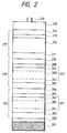
Fig. 2 is an example of a schematic sectional view to show a stack cell type photovoltaic element according to the present invention. It is, however, noted that the present invention is by no means intended to be limited to the photovoltaic element in the structure of Fig. 2.
-
The stack cell type photovoltaic element shown in Fig. 2 is of the laminate structure of three pin junctions, in which 219 is a first pin junction when counted from the light incidence side, 218 is a second pin junction, and 217 a third pin junction. These three pin junctions are stacked on a back electrode 202 formed on a substrate 201, and a transparent electrode 215 and a collector electrode 216 are formed on the top of the three pin junctions, thus forming the stack cell type photovoltaic element.
-
Each of the pin junctions 217, 218, and 219 shown in Fig. 2 has a first conduction type (n-type/p-type) semiconductor layer 203, 207, or 211, an i- type semiconductor layer 271, 272, or 212, a layer A 205, 209, or 213 forming a second conduction type (p-type/n-type) semiconductor layer, and a layer B 206, 210, or 214 forming the second conduction type (p-type/n-type) semiconductor layer. Fig. 2 illustrates the example of the pin junctions 217 and 218 in each of which the i-layer 271 or 272 is composed of three regions. Each i-layer 271 or 272 has RF i- layers 251, 261 or 252, 262 formed utilizing the RF (radio frequency) band as discharge frequency and a µw i-layer 204 or 208 formed utilizing the microwave (µ wave) band as discharge frequency.
-
These regions are provided as a result from such reasons that use of microwave enables high-speed film formation of the i-layers 271, 272 so as to obtain a necessary film thickness in a short period of time and that use of RF wave totally improves characteristics of the i-layers 271 and 272.
-
Therefore, the i-layer 271 or 272 may be formed as a single region, if desired characteristics are attained thereby.
-
The description was focused on the case where three pin junctions were stacked with reference to Fig. 2, but two or three or more pin junctions may be stacked with necessity. In that case, the absorption coefficient of light and the power generation efficiency should be taken into full consideration.
-
As explained with the photovoltaic element of Fig. 1, the locations of the doping layer and electrode will be switched depending upon the direction of incidence of light.
-
Fig. 5 is a schematic sectional view to show a suitable example of structure of another photovoltaic element. In Fig. 5, portions denoted by the same reference numerals as those in Fig. 1 represent the same portions. The element shown in Fig. 5 is an example in which the substrate 101 also serves as a back electrode.
-
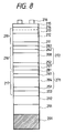
Fig. 8 is a schematic sectional view to show an example of structure of still another preferred photovoltaic element. In Fig. 8, portions denoted by the same reference numerals as those in Fig. 2 represent the same portions. The element shown in Fig. 8 is formed in the same triple cell arrangement as the element shown in Fig. 2, but it is mainly different from the element shown in Fig. 2 in that only the cell closest to the light incidence side (the top cell) has the layer A and in that the semiconductor layers are formed through a buffer layer 292 after a reflective and conductive layer 291 is formed on the substrate 201. In the drawing reference numerals 281 and 282 each denote second conduction type semiconductor layers.
-
The layers forming the photovoltaic elements of the present invention, described above, will be described in detail in the forming order.
(Substrate)
-
The substrate applied in the present invention can be properly selected with necessity, but it needs to be one at least permitting the semiconductor layers etc. to be formed thereon, as described above.
-
There is no specific restriction on the crystal form of such a substrate (for example, it may be either of single crystal or of non-single-crystal). Its electric property may be either conductive or insulating and may be properly selected depending upon the total structure of photovoltaic apparatus or upon procedures and steps of fabrication thereof. Its optical property may be either transparent or non-transparent.
-
However, a preferably used substrate is one having less deformation or distortion but having desired strength.
-
Specific examples of the material for the substrate include thin plates of metals such as Fe, Ni, Cr, Al, Mo, Au, Nb, Ta, V, Ti, Pt, or Pb or alloys such as brass or stainless steel, and composites thereof; films or sheets of heat-resistant synthetic resins such as polyester, polyethylene, polycarbonate, cellulose acetate, polypropylene, polyvinyl chloride, polyvinylidene chloride, polystyrene, polyamide, polyimide, or epoxy, or composites thereof with glass fibers, carbon fibers, boron fibers, or metal fibers; thin plates of the aforementioned metals or resin sheets of the aforementioned resins coated with a metal thin film of a different material and/or an insulating thin film such as SiO2, Si3N4, Al2O3, or AlN by sputtering, vapor deposition, plating, or the like; glass, ceramics, and so on.
-
When the substrate is a metal or the like being electrically conductive, it may be used also as an electrode for directly taking an electric current out. Further, if the substrate is a synthetic resin or the like being electrically insulative, the electrode for taking the electric current out is desirably formed by a preliminary surface treatment in a process of plating, vapor deposition, sputtering, or the like of a so-called metal itself or an alloy, such as Al, Ag, Pt, Au, Ni, Ti, Mo, W, Fe, V, Cr, Cu, stainless steel, brass, nichrome, SnO2, In2O3, ZnO, or ITO, and a transparent and conductive oxide (TCO) on the surface on which the deposit films are to be formed.
-
Of course, regardless of whether the substrate is an electrically conductive one such as the metals or not, a different metal layer or the like may be provided on the side where the deposit films are to be formed on the substrate for the purposes of improving the reflectivity of the light having passed through the semiconductor layers (for example, long-wavelength light) on the substrate surface, preventing mutual diffusion of constituent elements between the substrate material and the deposit films, and so on. If the substrate is relatively transparent and the photovoltaic element is constructed in the layer structure in which the light is incident from the substrate side, it is desirable to preliminarily deposit the transparent and conductive oxide or a conductive thin film such as a metal thin film on the substrate.
-
The surface of the substrate may be either a so-called smooth surface or a finely roughened surface. When the surface of the substrate is a finely roughened surface, the roughness may be of a desired configuration including a sphere, a cone, a pyramid, or the like, but reflection of light on the surface becomes diffused reflection when the maximum height (Rmax) is preferably in the range of 0.05 µm to 2 µm. This can increase the optical pathlength of reflected light from the surface and can further improve the utilization factor of incident light.
-
The configuration of the substrate may be a plate, an elongate belt (band), a cylinder, or the like with a smooth surface or a roughened surface depending upon applications, and the thickness thereof is properly determined so as to be capable of forming the photovoltaic element as desired. If the photovoltaic element is desired to be provided with flexibility or if the light is incident from the substrate side, the substrate may be formed as thin as possible within the range to sufficiently demonstrate the function as a substrate. However, the thickness of the substrate is normally 10 or more µm in view of fabrication of substrate, handling thereof, mechanical strength, and so on.
-
Especially, when the substrate stated above is a belt substrate, a preferred material for the belt substrate suitably applicable is one having less deformation or distortion at temperatures necessary for fabrication of the semiconductor films, having desired strength, and having electrical conduction, and specific examples of the material include thin plates of metals such as stainless steel, aluminum and alloys thereof, iron and alloys thereof, or copper and alloys thereof, and composites thereof; the foregoing coated with a metal thin film of a different material and/or an electrically insulating thin film such as SiO2, Si3N4, Al2O3, or AlN by sputtering, vapor deposition, plating, or the like; sheets of heat-resistant resins such as polyimide, polyamide, polyethylene terephthalate, or epoxy or composites thereof with glass fibers, carbon fibers, boron fibers, or metal fibers the surface of which is treated to become electrically conductive by a method of plating, vapor deposition, sputtering, or coating of a metal alone or an alloy thereof, and a transparent and conductive oxide (TCO) or the like.
-
A desired thickness of the belt substrate is as thin as possible within the range to demonstrate the strength enough to maintain a curved shape formed when carried by a carrying means in view of the cost, storage space, and so on. Specifically, the thickness is preferably in the range of 0.01 mm to 5 mm, more preferably in the range of 0.02 mm to 2 mm, and most preferably in the range of 0.05 mm to 1 mm. When a thin film of a metal or the like is used, the thickness can be determined to be relatively thin while maintaining the desired strength.
-
A preferred width of the belt substrate is determined in the range to maintain uniformity of the plasma formed in each film-forming chamber and to suit module arrangement of photovoltaic element formed, and specifically, it is determined preferably in the range of 5 cm to 100 cm, and more preferably in the range of 10 cm to 80 cm.
-
There is no specific limitation on the length of the belt substrate. It may be of a length enough to be rolled up in a roll form or it may be formed in an elongated shape formed by welding or the like of elongate strips.
-
When a reflective and conductive film for improving the reflectivity on the substrate surface is formed on the substrate, as described above, specific examples of suitable materials for the reflective and conductive film include Ag, Al, Cr, Au, Cu, and so on.
-
In the cases where the buffer layer is formed for preventing the mutual diffusion of constituent elements between the substrate material and the semiconductor films and for preventing short circuit, a transparent and conductive oxide film is preferably formed on the side of fabrication between the substrate and the semiconductor films. A suitable example of a material for the transparent and conductive oxide layer is ZnO.
(Back electrode and light reflecting layer)
-
The back electrode in the present invention is an electrode disposed on the surface of the semiconductor layer opposite to the light incidence side. Thus, the back electrode is placed on the substrate, or at a position on the opposite side to the substrate through the semiconductor layers when the substrate is transparent and the light is incident from the substrate side.
-
Specific examples of the material for the back electrode include metals such as gold, silver, copper, aluminum, nickel, iron, chromium, molybdenum, tungsten, titanium, cobalt, tantalum, niobium, zirconium, or the like or alloys such as stainless steel. Among them, metals with high reflectivity, such as aluminum, copper, silver, or gold, are particularly preferred. When a metal with high reflectivity is used, the back electrode can also serve as a light reflecting layer for reflecting light not absorbed by the semiconductor layers back toward the semiconductor layers.
-
The back electrode may be flat, but is more preferably roughened for scattering light. When the back electrode is roughened for scattering the light, it scatters the long-wavelength light not absorbed by the semiconductor layers so as to extend the optical pathlength in the semiconductor layers, to enhance long-wavelength sensitivity of photovoltaic element and to increase the short-circuit current, whereby the photoelectric conversion efficiency can be increased. It is desired to determine the roughened configuration for scattering the light so that differences between peaks and bottoms of the roughened configuration drop in the range of Rmax being 0.05 µm to 2.0 µm, and more preferably in the range of 0.2 µm to 2.0 µm.
-
In some cases of the substrate also serving as a back electrode, the back electrode does not always have to be formed.
-
The back electrode is formed using vapor deposition, sputtering, plating, printing, or the like. If the back electrode is formed in the roughened configuration for scattering the light, it is formed by subjecting a film of a metal or an alloy formed to dry etching, wet etching, sandblasting, heating, or the like. The roughened configuration for scattering the light can also be formed by vapor-depositing the aforementioned metal or alloy while heating the substrate.
-
An anti-diffusion layer such as conductive zinc oxide may be further provided, though not shown, between the back electrode 102 and the first conduction type (n-type) semiconductor layer 103. Effects of the anti-diffusion layer are to prevent metal elements constituting the back electrode 102 from diffusing into the n-type semiconductor layer, to prevent short circuit from occurring at a defect such as a pinhole between the back electrode 102 and the transparent electrode 107 provided on either side of the semiconductor layers by provision of a little resistance, to cause multiple interference by a thin film to confine the light incident in the photovoltaic element, and so on.
(Semiconductor layer)
-
Specific examples of materials suitably applicable for the semiconductor layer in the present invention include non-single-crystal materials containing a IV-group element such as Si, C, or Ge, or a IV-group alloy such as SiGe, SiC, or SiSn.
-
Among the above semiconductor materials, examples of semiconductor materials especially suitably used for the photovoltaic apparatus of the present invention include a-Si : H (hydrogenated amorphous silicon), a-Si : F (fluorinated amorphous silicon), a-Si : H : F (hydrogenated and fluorinated amorphous silicon), a-SiGe : H (hydrogenated amorphous silicon germanium), a-SiGe : F (fluorinated amorphous silicon germanium), a-SiGe : H : F (hydrogenated and fluorinated amorphous silicon germanium), a-SiC : H (hydrogenated amorphous silicon carbide), a-SiC : F (fluorinated amorphous silicon carbide), a-SiC : H : F (hydrogenated and fluorinated amorphous silicon carbide), or IV-group element based and IV-group alloy based non-single-crystal semiconductor materials containing microcrystals thereof.
-
The semiconductor layers can be modified by valence electron control and bandgap control. Specifically, it is realized by introducing a stock compound containing an element to become a valence electron controlling agent or a bandgap controlling agent into a film-forming space singly or in a mixture form with the stock gas for forming the deposit film or with the dilute gas, described previously, upon formation of semiconductor layer.
-
The valence electron control makes at least some parts of the semiconductor layers doped in the first conduction type (the p-type or the n-type) and in the second conduction type (the n-type or the p-type opposite to the first conduction type), thereby forming at least one pin junction. When a plurality of pin junctions are stacked, a so-called stack cell structure is accomplished.
-
Methods for forming the semiconductor layers may be selected from various CVD processes such as the microwave plasma CVD process, the RF plasma CVD process, the photo-assisted CVD process, the thermal CVD process, and the MOCVD process, various vapor deposition processes such as the EB vapor deposition, MBE, ion plating, and ion beam process, sputtering, spraying, printing, and so on. The plasma CVD process for decomposing the stock gas by plasma and depositing a film on the substrate is favorably used as a method industrially employed. A batch type apparatus or a continuous film-forming apparatus can be used as a reaction apparatus as occasion demands.
-
Below described in further detail are the semiconductor layers using the IV-group element based and IV-group alloy based non-single-crystal semiconductor materials especially suitably applicable for the photovoltaic apparatus of the present invention.
(1) i-type semiconductor layer (intrinsic semiconductor layer)
-
Especially in the photovoltaic elements using the IV-group element based and IV-group alloy based non-single-crystal semiconductor materials, the i-type layer used in the pin junction is an important layer for generating and transporting carriers with reception of irradiation light.
-
The i-type layer may be a layer including a small p-type part or a small n-type part as long as it can function substantially as an i-type layer.
-
The IV-group element based and IV-group alloy based non-single-crystal semiconductor materials may contain hydrogen atoms (H, D) or halogen atoms (X), as described above.
-
The hydrogen atoms (H, D) or halogen atoms (X) contained in the i-type layer function to compensate for uncoupled bonds (dangling bonds) in the i-type layer and to improve a product of mobility and life of carriers in the i-type layer. They also function to compensate for the interface levels in each interface between the p-type layer and the i-type layer or between the n-type layer and the i-type layer, so as to present the effect to improve the photoelectromotive force, photocurrent, and optical response of the photovoltaic element.
-
An optimum content of the hydrogen atoms or/and halogen atoms contained in the i-type layer is 1 to 40 atomic %. Especially, it is preferred that the hydrogen atoms or/and halogen atoms be distributed at higher contents on the side of each interface between the p-type layer and the i-type layer or between the n-type layer and the i-type layer. A preferably range of the contents of the hydrogen atoms or/and halogen atoms near the interfaces is 1.1 to 2 times greater than the content thereof in the bulk (at a position apart from the interfaces, for example, in a region near the center in the thickness direction). Further, a preferable arrangement is such that the content of the hydrogen atoms or/and halogen atoms changes according to the content of silicon atoms.
-
In the stack cell type photovoltaic element, a desired arrangement is such that a material for the i-type semiconductor layer in a pin junction close to the light incidence side is a material with a wide bandgap while a material for the i-type semiconductor layer in a pin junction apart from the light incidence side is a material with a narrow bandgap. An amorphous semiconductor material is preferably used as a material for the i-type semiconductor layer.
-
For example, amorphous silicon and amorphous silicon germanium are expressed with an element or elements for compensating for the dangling bonds, as a-Si : H, a-Si : F, a-Si : H : F, a-SiGe : H, a-SiGe : F, a-SiGe : H : F, or the like.
-
Preferable characteristics of the i-type semiconductor layer suitably applicable for the photovoltaic element of the present invention are as follows: the content of hydrogen atoms (CH) is 1.0 to 25.0 %; photoconductivity (σp) under irradiation with pseudo sunlight of AM 1.5 and 100 mW/cm2 is 1.0 × 10⁻⁷ or more S/cm; dark conductivity (σd) is 1.0 × 10⁻⁹ or less S/cm; Urback energy by the constant photocurrent method (CPM) is 55 or less meV; localized level density is 10 or less /cm.
-
By the valence electron control the semiconductor layers, at least some parts thereof, are doped in the first conduction type (the p-type or the n-type) and in the second conduction type (the n-type or the p-type opposite to the first conduction type), thereby forming at least one pin junction. When a plurality of pin junctions are stacked, a so-called stack cell structure is achieved.
(2) p-type semiconductor layer or n-type semiconductor layer
-
The p-type semiconductor layer or the n-type semiconductor layer in the present invention is a layer for constituting the first conduction type semiconductor layer and the second conduction type semiconductor layer (layer A, layer B), characterizing the photovoltaic element of the present invention, and it is an important layer for influencing the characteristics thereof.
-
A non-single-crystal material is suitably applicable for the material for the p-type semiconductor layer or the n-type semiconductor layer. The "non-single-crystal material" in the present invention means an amorphous material (expressed by a-), a microcrystalline material (expressed by µc-), and a polycrystalline material (expressed by poly-).
-
Specific examples of the amorphous material or the microcrystalline material include materials obtained by adding a high concentration of a p-type valence electron controlling agent (the III-group atoms such as B, Al, Ga, In, and Tl in the Periodic Table) or an n-type valence electron controlling agent (the V-group atoms such as P, As, Sb, and Bi in the Periodic Table) to a-Si : H, a-Si : HX, a-SiC : H, a-SiC : HX, a-SiGe : H, a-SiGe : HX, a-SiGeC : H, a-SiGeC : HX, a-SiO : H, a-SiO : HX, a-SiN : H, a-SiN : HX, a-SiON : H, a-SiON : HX, a-SiOCN : H, a-SiOCN : HX, µc-Si : H, µc-Si : HX, µc-SiC : H, µc-SiC : HX, µc-SiO : H, µc-SiO : HX, µc-SiN : H, µc-SiN : HX, µc-SiGeC : H, µc-SiGeC : HX, µc-SiON : H, µc-SiON : HX, µc-SiOCN : H, µc-SiOCN : HX, or the like.
-
Specific examples of the polycrystal material (expressed by poly-) include materials obtained by adding a high concentration of a p-type valence electron controlling agent (the III-group atoms such as B, Al, Ga, In, and Tl in the Periodic Table) or an n-type valence electron controlling agent (the V-group atoms such as P, As, Sb, and Bi in the Periodic Table) to poly-Si : H, poly-Si : HX, poly-SiC : H, poly-SiC : HX, poly-SiO : H, poly-SiO : HX, poly-SiN : H, poly-SiN : HX, poly-SiGeC : H, poly-SiGeC : HX, poly-SiON : H, poly-SiON : HX, poly-SiOCN : H, poly-SiOCN : HX, poly-Si, poly-SiC, poly-SiO, poly-SiN, or the like.
-
Especially, a crystalline semiconductor layer of less absorption of light or an amorphous semiconductor layer with a wide bandgap is suitable for the p-type layer or the n-type layer on the light incidence side.
-
A desirable additive amount of the III-group atoms in the Periodic Table into the p-type layer and a desired additive amount of the V-group atoms in the Periodic Table into the n-type layer are 0.1 to 50 atomic %.
-
The hydrogen atoms (H, D) or halogen atoms contained in the p-type layer or in the n-type layer function to compensate for the uncoupled bonds in the p-type layer or in the n-type layer to increase the doping efficiency of the p-type layer or the n-type layer. The hydrogen atoms or halogen atoms are added preferably in the range of 0.1 to 40 atomic % into the p-type layer or into the n-type layer. Especially when the p-type layer or the n-type layer is crystalline, the hydrogen atoms or the halogen atoms are added preferably in the range of 0.1 to 8 atomic %.
-
A preferred distribution form is a distribution of contents in which the hydrogen atoms or/and halogen atoms are distributed more on the side of each interface between the p-type layer and the i-type layer or between the n-type layer and the i-type layer, and a preferable range of the contents of the hydrogen atoms or/and halogen atoms near the interfaces is a range 1.1 to 2 times greater than the contents in the bulk.
-
Defect level density or mechanical distortion near the interfaces can be decreased by the arrangement in which the content of the hydrogen atoms or halogen atoms is increased near each interface between the p-type layer and the i-type layer or between the n-type layer and the i-type layer, whereby the photoelectromotive force and photocurrent of photovoltaic element of the present invention can be increased.
-
As an electric property of the p-type layer and the n-type layer in the photovoltaic element the activation energy is preferably 0.2 or less eV and more preferably 0.1 or less eV. Further, the resistivity is preferably 100 or less Ωcm and more preferably 1 or less Ωcm. Further, the film thickness of the p-type layer and the n-type layer is preferably in the range of 1 to 50 nm and more preferably in the range of 3 to 10 nm.
(3) Methods for forming the semiconductor layers
-
Specific examples of fabrication processes suitable for forming the IV-group element based and IV-group alloy based amorphous semiconductor layers suitable for the semiconductor layers in the photovoltaic apparatus of the present invention include the plasma CVD processes using an alternating current or high frequency waves, such as the RF plasma CVD process or the microwave plasma CVD process.
-
The microwave plasma CVD process is a method for forming a desired deposit film on a substrate placed in a deposition chamber, in which a material gas including a stock gas, a dilute gas, etc. is introduced into the deposition chamber (vacuum chamber), which can be set into a reduced-pressure state, the internal pressure in the deposition chamber is set at a desired pressure as evacuating the inside by a vacuum exhaust pump, microwaves oscillated by a microwave power supply are guided through a waveguide tube and through a dielectric window (alumina ceramics or the like) into the deposition chamber, and the material gas is decomposed to produce plasma thereof, thereby forming a desired deposit film on the substrate set in the deposition chamber. The microwave plasma CVD process can form deposit films applicable for the photovoltaic apparatus, under wide deposition conditions.
-
When a semiconductor layer for photovoltaic apparatus of the present invention is deposited by the microwave plasma CVD process, preferable conditions are as follows: the substrate temperature in the deposition chamber is between 100 and 450 °C; the internal pressure is between 0.5 and 30 mTorr; the microwave power is between 0.01 and 1 W/cm3; the frequency of microwave is between 0.1 and 10 GHz.
-
When a semiconductor layer is deposited by the RF plasma CVD process, preferable conditions are as follows: the substrate temperature in the deposition chamber is between 100 and 350 °C; the internal pressure is between 0.1 and 10 Torr; the RF power is between 0.001 and 5.0 W/cm3; the deposition rate is between 0.01 and 3 nm/sec.
-
Specific examples of the stock gas suitable for deposition of the IV-group element based and IV-group alloy based amorphous semiconductor layers suitable for the photovoltaic apparatus of the present invention include gasifiable compounds containing the silicon atom, gasifiable compounds containing the germanium atom, gasifiable compounds containing the carbon atom, and mixture gases of the foregoing compounds.
-
Specific examples of the gasifiable compounds containing the silicon atom include chain or cyclic silane compounds, and more specifically, gas states or readily gasifiable states of SiH4, Si2H6, SiF4, SiFH3, SiF2H2, SiF3H, Si3H8, SiD4, SiHD3, SiH2D2, SiH3D, SiFD3, SiF2D2, Si2D3H3, (SiF2)5, (SiF2)6, (SiF2)4, Si2F6, Si3F8, Si2H2F4, Si2H3F3, SiCl4, (SiCl2)5, SiBr4, (SiBr2)5, Si2Cl6, SiHCl3, SiH2Br2, SiH2Cl2, Si2Cl3F3, and so on.
-
Specific examples of the gasifiable compounds containing the germanium atom include GeH4, GeD4, GeF4, GeFH3, GeF2H2, GeF3H, GeHD3, GeH2D2, GeH3D, Ge2H6, Ge2D6, and so on.
-
Examples of elements for expanding the bandgap of the i-type semiconductor layer used in forming the first p-type semiconductor layer in the photovoltaic element of the present invention include carbon, oxygen, nitrogen, and so on. Specific examples of the gasifiable compounds containing the carbon atom include CH4, CD4, CnH2n+2 (n is an integer), CnH2n (n is an integer), C2H2, C6H6, CO2, CO, and so on. Specific examples of gases containing nitrogen include N2, NH3, ND3, NO, NO2, N2O, and so on. Specific examples of gases containing oxygen include O2, CO, CO2, NO, NO2, N2O, CH3CH2OH, CH3OH, and so on.
-
Examples of the substance introduced for valence electron control into the p-type layer or into the n-type layer are the III-group atoms and the V-group atoms in the Periodic Table.
-
Examples of starting materials effectively used for introducing the III-group atoms are as follows. Specific examples of the starting materials for introducing boron atoms include boron hydrides such as B2H6, B4H10, B5H9, B5H11, B6H10, B6H12 or B6H14 and boron halides such as BF3 or BCl3. In addition, further starting materials applicable include AlCl3, GaCl3, InCl3, TlCl3, and so on. Especially, B2H6 and BF3 are suitable.
-
Examples of starting materials effectively used for introducing the V-group atoms are as follows. Specific examples of the starting materials for introducing phosphorus atoms include phosphorus hydrides such as PH3 or P2H4 and phosphorus halides such as PH4I, PF3, PH5, PCl3, PCl5, PBr3, PBr5, or PI3. In addition, further materials applicable include AsH3, AsF3, AsCl3, AsBr3, AsF5, SbH3, SbF3, SbF5, SbCl3, SbCl5, BiH3, BiCl3, and BiBr3. Especially, PH3 and PF3 are suitable.
-
The gasifiable compound may be introduced into the deposition chamber as properly diluted with a gas of H2, He, Ne, Ar, Xe, Kr, or the like, or a gas selected from these may be separately introduced into the deposition chamber.
-
Particularly, for depositing a microcrystalline or polycrystalline semiconductor or a layer with less absorption of light or with a wide bandgap, such as a-SiC : H, preferred conditions are such that the stock gas is diluted at a dilution ratio of 2 to 100 with hydrogen gas and that the microwave power, or relatively high power as the RF power is applied.
(4) Fabrication process of layer A constituting the second conduction type (p-type or n-type) semiconductor layer
-
Next described is the fabrication process of the layer A constituting the second conduction type (p-type or n-type) semiconductor layer.
-
The layer A constituting the second conduction type (p-type or n-type) semiconductor layer is formed in such a manner that, after formation of the i-type semiconductor layer, the surface of the i-type semiconductor layer is exposed to plasma containing the p-type or n-type valence electron controlling agent whereby the i-type semiconductor layer near the surface is converted into the p-type or n-type region, or that the bandgap is further expanded.
-
More specifically, the plasma containing the p-type or n-type valence electron controlling agent means glow discharge plasma produced by application of DC, AC, or high frequency wave. The frequency applicable may be selected from various frequencies ranging DC to microwaves of approximately 10 GHz.
-
The material gas for forming the plasma is selected from stock gases suitable for deposition of the IV-group element based and IV-group alloy based amorphous semiconductor layers as described previously, gases containing substances suitable for the valence electron control as described previously, and mixtures thereof with the dilute gas as described previously.
-
Here, because the first p-type semiconductor layer or n-type semiconductor layer is not formed by deposition, the stock gases suitable for deposition of the IV-group element based and IV-group alloy based amorphous semiconductor layers stated above do not always have to be used. Even when the stock gas suitable for deposition of the IV-group element based and IV-group alloy based amorphous semiconductor layers is used, the forming conditions are selected so as to mainly cause the reaction for converting the i-type semiconductor layer near the surface into the p-type or n-type region or further to mainly cause injection of the element for expanding the bandgap of the i-type semiconductor layer, rather than the deposition reaction.
-
When the surface of the i-type semiconductor layer is exposed to such plasma, the p-type or n-type valence electron controlling agent and the element for expanding the bandgap of the i-type semiconductor layer are injected from the surface of the i-type semiconductor layer into a very shallow region, thereby converting the i-type semiconductor layer near the surface into the p-type or n-type region. The depth of the p-type or n-type region differs depending upon the conditions of plasma, but it is desirably between 1.0 nm and 10 nm.
-
This injection of the valence electron controlling agent and the element for expanding the bandgap of the i-type semiconductor layer into the i-type semiconductor layer by glow discharge plasma is utterly different from the conventional ion implantation used in crystal silicon or the like. In the conventional ion implantation ions are accelerated in a beam form and the energy of ions is high; whereas, in the injection by glow discharge plasma energy of the substances injected is low and they are injected from the surface of the i-type semiconductor layer only into a very shallow region. Fine control of depth of injection is also easy and uniform injection is readily effected across a large area.
-
Further, because the accelerated ions do not damage the surface of the i-type semiconductor layer, the doping layer with less local levels can be formed without deteriorating film quality of the i-type semiconductor layer. Accordingly, the layer A constituting the second conduction type (p-type or n-type) semiconductor layer can be formed uniformly across a large area and with good film quality.
-
Without use of the deposition reaction, there are other methods for causing the injection reaction of the valence electron controlling agent or the element for expanding the bandgap of the i-type semiconductor layer and examples thereof are the following three methods (a) to (c).
(a) Method in which the pressure of the mixture gas in the plasma state is set lower than the pressure upon normal deposition of the doping layer
-
To set the pressure of gas low can raise the injection efficiency of the valence electron controlling agent or the element for expanding the bandgap of the i-type semiconductor layer. The details of this mechanism are not clarified yet, but it is conceivably because the self bias of electrode becomes higher with a decrease of the pressure of gas, which increases the energy of positive ions decomposed in the plasma state. Another possible cause is an increase in mean free path of positive ions. Further, the valence electron controlling agent can be restricted from depositing on the surface of the i-type semiconductor layer, which can avoid the negative effect, such as an increase of light absorption coefficient, due to deposition of the valence electron controlling agent.
-
A preferred range of the gas pressure differs depending upon a type of the mixture gas, the frequency of power applied to the plasma, or input power, but, for example in the case of use of the RF CVD process, it is desirably between 0.01 and 1 Torr.
(b) Method in which the DC voltage, being a bias voltage, or AC power applied to the plasma is set higher than those upon normal deposition of the doping layer
-
To set the DC voltage or AC power higher can raise the injection efficiency of the valence electron controlling agent or the element for expanding the bandgap of the i-type semiconductor layer. The details of this mechanism are not clarified yet, but it is conceivably because the plasma potential becomes higher with an increase of the DC voltage or AC power, which raises the energy of the positive ions decomposed in the plasma state. It can also restrict the valence electron controlling agent from depositing on the surface of the i-type semiconductor layer.
-
A preferred range of the DC voltage or AC power differs depending upon a type of the mixture gas, the frequency of the power applied to the plasma, or the gas pressure, but, for example in the case of use of the RF CVD process, desired power is 0.01 or more W/cm3.
(c) Method for letting the mixture gas contain hydrogen
-
First, the plasma produces ions or radicals of hydrogen, which have etching effect, and therefore, even if the mixture gas contains a stock gas suitable for deposition of the aforementioned IV-group element based and IV-group alloy based amorphous semiconductor layers, an increase of the dilution ratio with hydrogen gas can control deposition of the stock gas, thus well injecting the valence electron controlling agent or the element for expanding the bandgap of the i-type semiconductor layer. It can also restrict the valence electron controlling agent from depositing on the surface of the i-type semiconductor layer.
-
Second, hydrogen atoms, as well as the valence electron controlling agent, are injected into the region near the surface of the i-type semiconductor layer, which work to compensate for uncoupled bonds (dangling bonds) in the i-type semiconductor layer, occurring due to injection of the valence electron controlling agent, and which can enhance an activation rate of acceptors or donors.
-
Third, when the hydrogen atoms are injected into the region near the surface of the i-type semiconductor layer, the bandgap of the i-type semiconductor layer is further expanded near the surface, light absorption is decreased in the first p-type semiconductor layer or n-type semiconductor layer to increase the short-circuit current (Jsc) of photovoltaic element, and the built-in potential is increased so as to raise the open-circuit voltage (Voc), whereby the photoelectric conversion efficiency can be improved.
-
A preferred range of the dilution ratio with hydrogen gas differs depending upon a type of the mixture gas, the frequency of power applied to the plasma, the power, or the gas pressure, but, for example in the case of use of the RF CVD process, a desired flow rate of hydrogen is 100 or more where 1 is taken as a flow rate of a sum of the stock gas suitable for deposition of the IV-group element based and IV-group alloy based amorphous semiconductor layers and the stock gas of the valence electron controlling agent.
(5) Fabrication process of the layer B constituting the second conduction type (p-type or n-type) semiconductor layer
-
The ordinary fabrication processes of p-type semiconductor layer or n-type semiconductor layer as explained in above (3) can be used for the fabrication process of the layer B constituting the second conduction type (p-type or n-type) semiconductor layer in the present invention.
-
However, the layer B constituting the second conduction type (p-type or n-type) semiconductor layer is desirably to be more heavily doped than the ordinary doping layers are and to have a smaller film thickness. A preferable range of the film thickness of the layer B constituting the second conduction type (p-type or n-type) semiconductor layer is between 1 nm and 10 nm.
-
The frequency of the power used in forming the layer A is preferably set lower than the frequency of the power used in forming the layer B. In this case, the frequency upon forming the layer A is desirably selected from the range of 5 to 500 kHz while the frequency upon forming the layer B is desirably selected from the range of 1 to 100 MHz. Preferred discharge power this time is between 0.01 and 5 W/cm2 for the layer A and between 0.0001 and 1 W/cm2 for the layer B.
-
Namely, the first p-type (n-type) semiconductor layer (which is the layer A constituting the second conduction type semiconductor layer) is formed by plasma doping using the discharge power of a lower frequency than the frequency of the high-frequency power used in the step for forming the second p-type (n-type) semiconductor layer (which is the layer B constituting the second conduction type semiconductor layer), whereby impurity ions are first injected with efficiency into the surface of the i-type semiconductor layer, thereby forming the first p-type (n-type) semiconductor layer containing crystalline substance. Next, the second p-type (n-type) semiconductor layer consisting of only amorphous substance is formed on the first p-type (n-type) semiconductor layer by the RF plasma CVD process, whereby the stacked semiconductor films for the photovoltaic element with a high photoelectric conversion efficiency can be formed across a large area and without dispersion or unevenness of characteristics.
-
The detailed mechanism of the above action is not clarified yet, but the following points can be considered.
-
Upon forming the layer A containing the crystalline substance by plasma doping the impurity ions are first injected into the surface of the i-type semiconductor layer and the outermost surface of the layer A is greatly damaged. Thus, it is considered that there exists many surface levels especially in the crystalline region. After the transparent electrode is formed on the layer A, the surface levels become interface levels between the transparent electrode and the p-type (or n-type) semiconductor layer, which increases the activation energy at the outermost surface of the p-type (or n-type) semiconductor layer or which distorts the internal potential in the photovoltaic element as trapping the carriers. Thus, it is considered that the surface levels negatively affect movement of carriers between the transparent electrode and the p-type (or n-type) semiconductor layer.
-
In contrast with it, it is considered that the amorphous semiconductor can uniformly cover the surface levels existing in the outermost surface of the layer A greatly damaged, when the layer B consisting of only the amorphous substance is formed on the layer A by the RF plasma CVD process, which can decrease the surface levels.
-
As a result, the surface levels are prevented from negatively affecting the movement of carriers between the transparent electrode and the p-type (or n-type) semiconductor layer, whereby the stacked semiconductor layers for photovoltaic element with high photoelectric conversion efficiency can be formed across a large area and without dispersion or unevenness of characteristics, presumably.
(Transparent electrode)
-
The transparent electrode 107 in the present invention serves as an electrode on the light incidence side to transmit the light and also serves as an anti-reflection film in the optimum thickness. Requirements for the transparent electrode 107 are high transmittance in the wavelength region which the semiconductor layers can absorb, and low resistivity. Preferably, the transmittance at 550 nm is 80 or more % and more preferably 85 or more %. The resistivity is preferably 5 × 10⁻³ or less Ωcm and more preferably 1 × 10⁻³ or less Ωcm. Examples of materials preferably applicable for the transparent electrode include conductive oxides, such as In2O3, SnO2, ITO (In2O3 + SnO2), ZnO, CdO, Cd2SnO4, TiO2, Ta2O5, Bi2O3, MoO3, or NaxWO3, or mixtures thereof. An element (dopant) for changing the electric conductivity may be added to these compounds.
-
Examples of the element (dopant) for changing the electric conductivity are as follows. For example, in the case of the transparent electrode 107 being ZnO, they include Al, In, B, Ga, Si, and F; in the case of In2O3, they include Sn, F, Te, Ti, Sb, and Pb; and in the case of SnO2, they include F, Sb, P, As, In, Tl, Te, W, Cl, Br, and I.
-
A method for forming the transparent electrode 107 suitably applicable is the vapor deposition process, the CVD process, the spraying process, the spin-on process, the dipping process, or the like.
(Collector electrode)
-
The collector electrode 108 in the present invention is formed on a part of the transparent electrode 107 with necessity, where the resistivity of the transparent electrode 107 is not sufficiently low. It works to decrease the resistivity of the electrode so as to lower series resistance of photovoltaic element. Examples of a material for the collector electrode include metals such as gold, silver, copper, aluminum, nickel, iron, chromium, molybdenum, tungsten, titanium, cobalt, tantalum, niobium, or zirconium, alloys such as stainless steel, and conductive pastes using a powdered metal. It is formed in a branched pattern so as not to interrupt the incident light into the semiconductor layer.
-
An example of the configuration of the collector electrode is next explained referring to Fig. 3.
-
Fig. 3 is a schematic plan view of the photovoltaic element, observed from the light incidence side. As shown in Fig. 3, the branched configuration of the collector electrode 108 can decrease the substantial resistance with efficiency and without impeding the incident light from entering the element.
-
Further, as shown in Fig. 3, a more reduction of substantial resistance can be expected by increasing the width of strips horizontally extending in the branched pattern. In addition, output efficiency can be further improved by increasing the widths of the strips as the distance to the output decreases.
-
In the total area of the photovoltaic apparatus, an area occupied by the collector electrode is preferably 15 or less %, more preferably 10 or less %, and most preferably 5 or less %.
-
A mask is used for forming the pattern of the collector electrode, and a method for forming it may be the vapor deposition process, the sputtering process, the plating process, the printing process, or the like.
-
When a photovoltaic apparatus (module or panel) with desired output voltage and output current is fabricated using the photovoltaic elements of the present invention, the photovoltaic elements of the present invention are connected in series or in parallel, protection layers are formed on the top and bottom surfaces, and take-out electrodes of output etc. are attached. When the photovoltaic elements of the present invention are connected in series, a diode for preventing a reverse current is sometimes incorporated.
(Apparatus for fabricating photovoltaic element)
-
Examples of the fabricating apparatus of the photovoltaic element according to the present invention include the continuous forming apparatus of stacked semiconductor films as shown in Fig. 4 or Fig. 6. The apparatus of Fig. 4 is used when the form of the substrate is a plate (single plate type), while the apparatus of Fig. 6 is used when the form of the substrate is a belt (continuous type).
-
The fabrication apparatus of photovoltaic element according to the present invention will be explained in detail with reference to the drawings.
-
In Fig. 4, reference numeral 401 designates a load lock chamber (input room), 402 a carrying room (chamber) for the n-type layer (or the p-type layer), 403 a carrying room (chamber) for the i-layer, 404 a carrying room (chamber) for the p-type layer (or the n-type layer), and 405 an unload chamber (take-out room). Numerals 406, 407, 408, and 409 each denote gate valves, which are provided for communication between adjacent rooms or for establishing independence of each room. Numerals 410, 411, and 412 each denote heaters for heating the substrate, and numeral 413 denotes substrate carrying rails as a substrate carrying means. Numeral 417 represents a deposition chamber for formation of the n-type layer (or the p-type layer), 418 a deposition chamber for formation of the i-layer, and 419 a deposition chamber for formation of the p-type layer (or the n-type layer). Each deposition chamber 417, 419 has an RF introducing cup 420 or 421 connected to an RF power supply 422 or 423, inside thereof. A gas supply pipe 429, 449, 469 is connected to each deposition chamber, whereby a desired gas can be supplied into each deposition chamber. A microwave introducing pipe 426 is connected through a microwave introducing window 425 to the deposition chamber 418, so that microwaves generated by a microwave generating means not shown can be guided through the microwave introducing pipe 426 and the microwave introducing window 425 into the deposition space. Numeral 424 designates a bias applying power supply for generating a bias voltage applied to the deposition chamber (or to the substrate in the chamber). An enlarged view of the deposition chamber for forming the i-layer is shown in a circle in the drawing, and, as shown inside the circle, the bias power supply is electrically connected to a bias electrode set inside the deposition space. Numeral 427 is a shutter, which is opened or closed with necessity. When the shutter 427 is open, the i-layer is formed on the substrate 490. The heating heaters 410, 411, and 412 are movable in the directions of arrows. Each heater is moved with necessity from the side of carrying rails 413 to the deposition chamber 417, 418, 419 together with the substrate 490, and the substrate 490 can be moved from the side of the deposition chamber 417, 418, 419 to the carrying rails 413.
-
It is needless to mention that an exhaust means such as a vacuum pump, not shown, is connected through a conductance valve not shown to each chamber.
-
Fig. 6 is a schematic explanatory drawing to show a basic example of the continuous forming apparatus for continuously forming the stacked semiconductor films according to the present invention. In Fig. 6, the continuous forming apparatus of stacked semiconductor films according to the present invention is basically composed of a feeding chamber 601 of belt substrate, a film-forming chamber 602 for forming the n-type semiconductor layer (i.e., the first conduction type semiconductor layer) by the RF plasma CVD process, an i-type semiconductor layer forming chamber 603 for forming the i-type semiconductor layer by the RF plasma CVD process, a film-forming chamber 604 for forming the first p-type semiconductor layer (i.e., the layer A constituting the second conduction type semiconductor layer) by plasma doping, a film-forming chamber 611 for forming the second p-type semiconductor layer (i.e., the layer B constituting the second conduction type semiconductor layer) by the RF plasma CVD process, and a winding chamber 605 for winding up the belt substrate. Gas gates 606 connect the chambers with each other.
-
In the apparatus of the present invention, the belt substrate 607 is fed out from a bobbin 608 in the feeding chamber 601 of belt substrate and is carried through the four film-forming chambers connected by the gas gates before rolled up on a bobbin 609 in the belt substrate winding chamber 605. While the substrate is carried through the four film-forming chambers, the stacked films of non-single-crystal semiconductors are formed in the nip structure on the surface thereof.
-
Fig. 7 is a schematic sectional view for explaining an example of the film-forming chambers in the apparatus shown in Fig. 6. In Fig. 7, reference numeral 701 designates a belt substrate, 702 a vacuum container, 703, 704 gas gates, 705 a discharge chamber, 706 a discharge electrode, 707 a stock gas introducing pipe, 708 an exhaust pipe, 709 a block heater, 710 a discharge chamber-to-outside exhaust port, 711 a forming region aperture adjusting plate, 712 a film-forming chamber lid, 713, 714 heaters, 715, 716 thermocouples, 717 a reflector, 718 support rollers, 719 a separation passage, and 720 a gate gas introducing pipe.
-
As shown, the belt substrate 701 is guided into or out of the film-forming space through the gas gate 703 or 704. In the gas gate 703, 704 a gas giving no negative effect on the film formation, such as He gas or H2 gas, is supplied through the gate gas introducing pipe 720 into the separation passage 719, whereby separation can be made between the outstanding chamber and another film-forming room (chamber) adjacent thereto or between the outstanding chamber and the atmosphere. The pressure inside the vacuum container 702 can be decreased by the exhaust means such as a vacuum pump through the exhaust pipe 708. In the case of the structure shown in Fig. 7, not only the film-forming space but also the space around it can be evacuated through the discharge chamber-to-outside exhaust port 710. The belt substrate 701, supplied through the separation passage 719, is carried into the film-forming space while the position thereof is regulated by the support rollers 718. In the film-forming space the substrate 701 can be heated at a desired temperature by the heaters 713, 714 utilizing lamp heaters such as halogen lamps. The reflector 717 is provided on the opposite side of the heaters 713, 714 to the substrate 701, so that heat from the heaters 713, 714 such as lamp heaters can be reflected toward the substrate with efficiency. The discharge electrode 706 is disposed as facing to the film-forming surface of the substrate 701, and the block heater 709 is disposed on the opposite side of the discharge electrode 706 to the substrate 701. The stock gas is supplied through the stock gas introducing pipe 707 to the back face of the block heater 709 and is emitted from here into the film-forming space. The substrate 701, having passed through the film-forming space, is carried through the gas gate 704 as supported by the supporting rollers 718 in the same manner as when entering the film-forming space.
-
Fig. 9 is a schematic, sectional, structural drawing to explain an example of the film-forming apparatus having a triple cell structure.
-
In Fig. 9, reference numeral 901 designates a feeding chamber for the belt substrate, A a film-forming chamber set for forming a bottom cell in the lowest part, B a film-forming chamber set for forming a middle cell in a middle part, C a film-forming chamber set for forming a top cell in the outermost part, 902A, 902B, 902C film-forming chambers each for forming the first conduction type semiconductor layer utilizing the RF plasma, 903A, 903B, 903C, 911A, 911B film-forming chambers for forming the i-type semiconductor layer utilizing the RF plasma, 910A, 910B film-forming chambers for forming the i-type semiconductor layer utilizing the microwave plasma, 904A, 904B, 911C film-forming chambers for forming the second conduction type semiconductor layer utilizing the RF plasma, 904C a film-forming chamber for forming the second conduction type semiconductor layer (the layer A) by plasma doping, 905 a winding chamber for the belt substrate, 906 gas gates, 907 a belt substrate, 908 a feeding bobbin of belt substrate, and 909 a winding bobbin of belt substrate.
-
In Fig. 9, the belt substrate 907 is fed out from the feeding bobbin 908, is carried through the gas gates 906 and the respective film-forming rooms (chambers) continuously arranged as the films are formed thereon, and is again wound up on the winding bobbin on the opposite side.
-
Fig. 9 shows the arrangement of film-forming chambers along the arcuate configuration of the belt substrate 907, which is employed because deflection of the substrate 907 due to its own weight is taken into account in order to carry the substrate more smoothly.
-
Fig. 10 is a schematic sectional view for explaining a suitable example of the film-forming chamber utilizing the microwave, applicable to the film-forming chambers shown in Fig. 9 (or Fig. 6). In the drawing, portions denoted by the same reference numerals as those shown in Fig. 7 represent the same members.
-
Numeral 1002 represents a discharge chamber unit, 1009 a conductance valve, 1010 an exhaust pipe for primary evacuation, 1014 a bias electrode, 1021 a microwave introducing window, 1022 a perforated partition plate, 1023 a pressure measuring pipe, 1024 a forming chamber temperature adjuster, and 1025 a substrate temperature adjuster (a heater or the like).
-
It is a matter of course that the apparatus as described above can be properly modified as occasion demands.
-
The photovoltaic element having the non-single-crystal silicon based semiconductor material will be explained in detail, but it is noted that the present invention is by no means limited by the description in the following.
-
Examples 1 to 10 were carried out to investigate the cases where the second conduction type semiconductor layer had the layer A formed by exposing the surface of the i-type semiconductor layer to the plasma containing the valence electron controlling agent and the layer B deposited on the layer A by the CVD process using at least the valence electron controlling agent and the main constituent element of the i-type semiconductor layer.
-
Examples 11 to 20 were carried out to investigate the cases where the layer A further contained the element for expanding the bandgap.
-
Examples 21 to 28 were carried out to investigate the cases where the layer B further contained the element for expanding the bandgap.
-
Examples 29 to 38 were carried out to investigate the cases where the layer A and the layer B each further contained the element for expanding the bandgap.
-
Examples 39 to 41 were carried out to investigate the discharge power and the frequency thereof used in forming the layer A and the layer B.
(Example 1)
-
In this example, the single cell type photovoltaic element shown in Fig. 1 was fabricated using the deposition apparatus of Fig. 4. Checked with this example was a case where the p-type semiconductor layer, being the second conduction type semiconductor layer, was comprised of the layer A formed by exposing the surface of the i-type semiconductor layer to the plasma containing the p-type valence electron controlling agent and the layer B formed on the surface of the layer A by depositing the p-type valence electron controlling agent and the main constituent element of the i-type semiconductor layer thereon.
-
A process for fabricating it will be explained according to its procedures.
- (1) A stainless steel support 101 of thickness 0.5 mm and size 50 × 50 mm2 was cleaned in acetone and isopropanol with ultrasonic waves, and thereafter was dried under warm air. After that, by the sputtering method, a light reflecting layer of Ag 0.3 µm thick was formed on the surface of the stainless steel support 101 at room temperature and a reflection enhancing layer of ZnO 1.0 µm thick was formed on the light reflecting layer at 350 °C, thus forming the back electrode 102. A resultant obtained through these steps was a substrate 490.
- (2) Using the deposition apparatus 400, the semiconductor layers each were formed on the substrate 490. The deposition apparatus 400 can perform both the microwave plasma CVD process and the RF plasma CVD process.
Stock gas bombs not shown are connected through gas introducing pipes to the deposition apparatus. The stock gas bombs all were of the grade refined at super-high purity, and they were SiH4 gas bomb, SiF4 gas bomb, SiH4/H2 (dilution rate: 10 %) gas bomb, CH4 gas bomb, C2H6 gas bomb, GeH4 gas bomb, GeF4 gas bomb, Si2H6 gas bomb, PH3/H2 (PH3 gas diluted with H2 at dilution rate: 2 %) gas bomb, BF3/H2 (dilution rate: 1 %) gas bomb, BF3/He (dilution rate: 1 %) gas bomb, H2 gas bomb, and He gas bomb, which were connected to the deposition apparatus.
- (3) The substrate 490 was placed on the substrate carrying rails 413 in the load chamber 401 and the inside of the load chamber 401 was evacuated to a vacuum by the unrepresented vacuum evacuation pump to the pressure of about 1 × 10⁻⁵ Torr.
- (4) Opening the gate valve 406, the substrate was carried into the carrying chamber 402 and deposition chamber 417 preliminarily evacuated to a vacuum by the unrepresented vacuum evacuation pump. The back face of the substrate 490 was heated in close contact with the substrate heating heater 410, and the inside of the deposition chamber 417 was evacuated to the pressure of about 1 × 10⁻⁵ Torr by the unrepresented vacuum evacuation pump. The above completed preparation for film formation.
- (5) For forming the RF n-type layer of a-Si (the n-type semiconductor layer formed by the RF plasma CVD process), H2 gas was introduced through the gas introducing pipe 429 into the deposition chamber 417 while the flow of H2 gas was controlled at 200 sccm by a mass flow controller not shown as opening a valve not shown. The pressure inside the deposition chamber 417 was adjusted to be 1.1 Torr by a conductance valve not shown.
- (6) The substrate heating heater 410 was set to keep the temperature of the substrate 490 at 350 °C. When the substrate temperature became stable, SiH4 gas and PH3/H2 gas were introduced through the gas introducing pipe 429 into the deposition chamber 417 as manipulating unrepresented valves. At this time, SiH4 gas was adjusted at 2 sccm, H2 gas at 50 sccm, and PH3/H2 gas at 0.5 sccm by unrepresented mass flow controllers, and the pressure inside the deposition chamber 417 was adjusted so as to be 1.1 Torr.
- (7) The power of the high frequency (hereinafter referred to as "RF") power supply 422 was set to 0.005 W/cm3, and the RF power was applied to the plasma forming cup 420 to cause glow discharge and to start formation of the RF n-type layer on the substrate. After the RF n-type layer was formed in the thickness of 20 nm, the RF power supply was turned off to stop the glow discharge, thus finishing the formation of the RF n-type layer 103.
- (8) Stopping the flow of SiH4 gas and PH3/H2 into the deposition chamber 417, H2 gas was let to continuously flow into the deposition chamber for five minutes. After that, the flow of H2 was also stopped, and the inside of the deposition chamber and gas pipe was evacuated to the vacuum of 1 × 10⁻⁵ Torr.
- (9) The i-type layer 104 of a-Si was formed by the microwave plasm CVD process. First, opening the gate valve 407, the substrate 490 was carried into the carrying chamber 403 and i-type layer deposition chamber 418 preliminarily vacuumized by the unrepresented vacuum evacuation pump. The back face of the substrate 490 was heated in close contact with the substrate heating heater 411, and the inside of the i-type layer deposition chamber 418 was vacuumized to the pressure of about 1 × 10⁻⁵ Torr by the unrepresented vacuum evacuation pump.
- (10) For fabricating the i-type layer, the substrate heating heater 411 was set to keep the temperature of the substrate 490 at 350 °C, and, after the substrate was sufficiently heated, valves not shown were gradually opened to let SiH4 gas and H2 gas flow through the gas introducing pipe 449 into the i-type layer deposition chamber 418. At this time, SiH4 gas was adjusted at 50 sccm and H2 gas at 100 sccm by respective mass controllers not shown. The pressure inside the i-type layer deposition chamber 418 was controlled at 5 mTorr by adjusting an aperture of a conductance valve not shown.
- (11) The RF power supply 424 was set at 0.50 W/cm3 and the power was applied to the bias electrode 428. After that, the power of the unrepresented microwave power supply was set at 0.20 W/cm3, and the microwave power was introduced through the microwave introducing waveguide tube 426 and microwave introducing window 425 into the i-type layer deposition chamber 418 to cause glow discharge. Then, opening the shutter 427, fabrication of the i-type layer was started on the n-type layer. After the i-type layer was formed in the thickness of 0.1 µm, the microwave glow discharge was stopped and the output of bias power supply 424 was turned off, thus completing the fabrication of the i-type layer 104.
- (12) Closing the valve not shown, the flow of SiH4 gas into the i-type layer deposition chamber 418 was stopped, and then H2 gas was let to continuously flow into the i-type layer deposition chamber 418 for two minutes. After that, closing the valve not shown, the inside of the i-type layer deposition chamber 418 and the gas pipe was evacuated to the vacuum of 1 × 10⁻⁵ Torr.
- (13) According to the following procedures, the i-type semiconductor layer of a-Si near the surface was converted into the p-type region to form the first p-type semiconductor layer or p1 layer (layer A) 105 by exposing the surface of the i-type semiconductor layer of a-Si to the plasma containing the p-type valence electron controlling agent.
First, opening the gate valve 408, the substrate 490 was carried into the carrying chamber 404 and p-type layer deposition chamber 419 preliminarily vacuumized by the unrepresented vacuum evacuation pump. The back face of the substrate 490 was heated in close contact with the substrate heating heater 412, and the inside of the p-type layer deposition chamber 419 was vacuumized to the pressure of about 1 × 10⁻⁵ Torr by the unrepresented vacuum evacuation pump.
The substrate heating heater 412 was set so as to keep the temperature of substrate 490 at 230 °C, and, after the substrate temperature became stable, He gas and BF3/He gas were introduced through the gas introducing pipe 469 into the deposition chamber 419 as manipulating the unrepresented valves. At this time, He gas was controlled at 50 sccm and BF3/He gas at 5 sccm by the unrepresented mass flow controllers and the pressure inside the layer deposition chamber 419 was controlled at 2.0 Torr by adjusting the aperture of the unrepresented conductance valve.
The power of the RF power supply 423 was set to 0.15 W/cm3 and the RF power was guided into the plasma forming cup 421 to cause glow discharge. Exposing the surface of the i-type semiconductor layer to the plasma containing the p-type valence electron controlling agent, the i-type semiconductor layer near the surface started to be converted into the p-type layer to form the first p-type semiconductor layer or p1 layer (layer A). After the layer was formed in the thickness of 3 nm, the RF power supply was turned off to stop the glow discharge, thus completing the formation of the first p-type semiconductor layer or p1 layer (layer A) 105.
- (14) Manipulating the unrepresented valves, the flow of He gas and BF3/He gas was stopped, and H2 gas was further let to flow at 50 sccm, SiH4/H2 gas at 0.5 sccm, BF3/H2 gas at 0.5 sccm, and CH4 gas at 5 sccm. The second p-type semiconductor layer or p2 layer (layer B) of a-Si was successively stacked on the first p-type semiconductor layer or p1 layer (layer A) by the RF plasma CVD process. At this time, the pressure inside the p-type layer deposition chamber 419 was controlled at 2.0 Torr by adjusting the aperture of the conductance valve not shown.
The power of the RF power supply 423 was set to 0.15 W/cm3 and the RF power was introduced to the plasma forming cup 421 to cause glow discharge, thus starting formation of the second p-type semiconductor layer or p2 layer (layer B) containing the main constituent element of the i-type semiconductor layer of a-SiC and the element for expanding the bandgap of the i-type semiconductor layer. After the RF p-type layer was formed in the thickness of 5 nm, the RF power supply was turned off to stop the glow discharge, thus completing the formation of the p-type layer of the present invention.
Closing the valves not shown, the flow of SiH4/H2 gas, BF3/H2 gas, and CH4 gas into the p-type layer deposition chamber 419 was stopped, and H2 gas was let to continuously flow into the p-type layer deposition chamber 419 for three minutes. After that, the flow of H2 was also stopped by closing the valve not shown, and the inside of the p-type layer deposition chamber 419 and the gas pipe was evacuated to the vacuum of 1 × 10⁻⁵ Torr.
- (15) Opening the gate valve 409, the substrate 490 was carried into the unload chamber 405 preliminarily vacuumized by the unrepresented vacuum evacuation pump, and the unload chamber 405 was let to leak by opening a leak valve not shown.
- (16) ITO was deposited as a transparent and conductive layer 107 in the thickness of 70 nm on the p-type layer by the vacuum vapor deposition process. Next, a mask with a comb-shaped aperture was mounted on the transparent and conductive layer 107, and the comb-shaped collector electrode 113 was deposited in the structure of Cr (40 nm)/Ag (1000 nm)/Cr (40 nm) in order by the vacuum vapor deposition process.
-
The foregoing concludes the fabrication of the photovoltaic element of this example (SC Ex 1).
(Comparative Example 1-1)
-
This example is different from Example 1 in that the first p-type semiconductor layer or p1 layer (layer A) was not formed. Further, the film thickness of the second p-type semiconductor layer or p2 layer (layer B) of a-Si was 8 nm.
-
The other points were the same as in Example 1.
-
The photovoltaic element fabricated in this example will be called as SC Comp Ex 1-1.
-
Next explained are evaluation tests which were carried out for six photovoltaic elements obtained in each of Example 1 and Comparative Example 1-1.
-
As the evaluation tests, V-I characteristics were observed while each photovoltaic element was placed under light irradiation of AM 1.5 (100 mW/cm
2). From the results, an average value was calculated for each of photoelectric conversion efficiency (η) of (photoelectromotive force)/(incident light power), open-circuit voltage (V
oc), short-circuit current (J
sc), and fill factor (F. F.). Table 1 shows the photoelectric conversion factor (η), open-circuit voltage (V
oc), short-circuit current (J
sc) and fill factor (F. F.) of (SC Ex 1), which were normalized with corresponding measured values of (SC Comp Ex 1-1) being 1.0.
TABLE 1 | | P-E conversion efficiency (η) | Open-ckt volt (Voc) | Short-ckt current (Jsc) | Fill factor (F. F) |
| (SC Ex 1) | 1.07 | 1.03 | 1.01 | 1.03 |
-
From Table 1, it was found that the photovoltaic elements of (SC Ex 1) were superior in the open-circuit voltage (Voc) and the fill factor (F. F.) as well as in the photoelectric conversion efficiency (η) to those of (SC Comp Ex 1-1).
-
In order to check the unevenness and dispersion in the substrate, a mask with twenty five holes (of the area of 0.25 cm
2) was set on the p-type layer and a film of ITO was formed as a transparent conductive layer in the thickness of 70 nm by the vacuum vapor deposition process. Table 2 shows results of unevenness and dispersion in substrate as to the open-circuit voltage (V
oc) and the fill factor (F. F.), measured for such samples. Here, a maximum value out of measured values in a same substrate was taken as 1.
TABLE 2 | | Open-ckt voltage (Voc) | Fill factor (F. F.) |
| (SC Ex 1) | 0.98 - 1.00 | 0.97 - 1.00 |
| (SC Comp Ex 1-1) | 0.90 - 1.00 | 0.95 - 1.00 |
-
From Table 2, it was found that the photovoltaic elements of (SC Ex 1) had less unevenness and dispersion in the substrate whereby uniformity of photoelectric conversion characteristics thereof was improved.
-
Further, in measuring the V-I characteristics of solar cell, a blue filter (HOYA B390) was used over AM 1.5 (100 mW/cm
2), thereby performing measurements to strongly reflect defect density on the light incidence side. Table 3 shows results of the photoelectric conversion efficiency (η), open-circuit voltage (V
oc), short-circuit current (J
sc), and fill factor (F. F.) measured for such samples. Each value in the table indicates a numerical value normalized with a corresponding measured value of (SC Comp Ex 1-1) being 1.0.
TABLE 3 | | P-E conversion efficiency (η) | Open-ckt volt (Voc) | Short-ckt current (Jsc) | Fill factor (F. F) |
| (SC Ex 1) | 1.09 | 1.03 | 1.01 | 1.05 |
-
From comparison of Table 3 with Table 1, it was found that an improvement in the fill factor (F. F.) in the measurement under the blue light was more noticeable than in the measurement under the white light.
-
It was concluded that this result showed that the interface levels in the p/i interface there decreased because almost all photocarriers occurred near the light incidence side of the i-type semiconductor layer under the blue light.
(Example 2)
-
This example is different from Example 1 in that the following conditions were employed instead of those in Example 1 in forming the second p-type semiconductor layer or p2 layer (layer B).
- (1) H2 gas was let to flow at 50 sccm, SiH4/H2 gas at 0.25 sccm, and BF3/H2 gas at 1 sccm.
- (2) The power of the RF power supply 423 was set to 0.15 W/cm3 to cause glow discharge and the layer was deposited under the conditions to form µc-Si by the RF plasma CVD process.
- (3) The film thickness of the RF p-type µc-Si layer was 5 nm.
-
The other points were the same as in Example 1.
-
The photovoltaic element fabricated in this example will be called as SC Ex 2.
(Comparative Example 2-1)
-
This example is different from Example 2 in that the first p-type semiconductor layer or p1 layer (layer A) was not formed. The film thickness of the second p-type semiconductor layer or p2 layer (layer B) of µc-Si was 8 nm.
-
The other points were the same as in Example 2.
-
The photovoltaic element fabricated in this example will be called as SC Comp Ex 2-1.
-
Next explained are evaluation tests which were carried out for six photovoltaic elements obtained in each of Example 2 and Comparative Example 2-1.
-
As the evaluation tests, V-I characteristics were observed while each photovoltaic element was placed under light irradiation of AM 1.5 (100 mW/cm
2). From the results, an average value was calculated for each of photoelectric conversion efficiency (η) of (photoelectromotive force)/(incident light power), open-circuit voltage (V
oc), short-circuit current (J
sc), and fill factor (F. F.). Table 4 shows the photoelectric conversion factor (η), open-circuit voltage (V
oc), short-circuit current (J
sc), and fill factor (F. F.) of (SC Ex 2), which were normalized with corresponding measured values of (SC Comp Ex 2-1) being 1.0.
TABLE 4 | | P-E conversion efficiency (η) | Open-ckt volt (Voc) | Short-ckt current (Jsc) | Fill factor (F. F) |
| (SC Ex 2) | 1.08 | 1.03 | 1.01 | 1.04 |
-
From Table 4, it was found that the photovoltaic elements of (SC Ex 2) were superior in the open-circuit voltage (Voc) and the fill factor (F. F.) as well as in the photoelectric conversion efficiency (η) to those of (SC Comp Ex 2-1).
(Example 3)
-
This example is different from Example 2 in that a-SiGe was used as a material for forming an MW i-type layer (an i-type semiconductor layer formed by the microwave CVD process) instead of a-Si.
-
A process for fabricating the MW i-type layer of a-SiGe will be explained according to its procedures.
- (1) The substrate heating heater 411 was set to keep the temperature of the substrate 490 at 380 °C and, gradually opening the valves not shown after the substrate was sufficiently heated, SiH4 gas, GeH4 gas, and H2 gas were let to flow through the gas introducing pipe 449 into the i-type layer deposition chamber 418. At this time, SiH4 gas was controlled at 50 sccm, GeH4 gas at 35 sccm, and H2 gas at 120 sccm by adjusting the respective mass flow controllers not shown. The pressure inside the i-type layer deposition chamber 418 was controlled at 6 mTorr by adjusting the aperture of the conductance valve not shown.
- (2) The RF power supply 424 was set to 0.2 W/cm3 to apply the power to the bias bar 428. After that, the power of the microwave power supply not shown was set to 0.1 W/cm3 and the microwave power was introduced through the microwave introducing waveguide pipe 426 and the microwave introducing window 425 into the i-type layer deposition chamber 418 to cause glow discharge. Then opening the shutter 427, fabrication of the MW i-type layer was started on the RF i-type layer. After the i-type layer was formed in the thickness of 0.15 µm, the microwave glow discharge was stopped and the output from the bias power supply 424 was turned off, thus completing the fabrication of the MW i-type layer 204.
- (3) Then the valves not shown were closed to stop the flow of SiH4 gas and GeH4 gas into the i-type layer deposition chamber 418. After that, H2 gas was let to continuously flow into the i-type layer deposition chamber 418 for two minutes. Then the valve not shown was closed and the inside of the i-type layer deposition chamber 418 and the gas pipe was evacuated to the vacuum of 1 × 10⁻⁵ Torr.
-
The other points were the same as in Example 2.
-
The photovoltaic element fabricated in this example will be called as SC Ex 3.
(Comparative Example 3-1)
-
This example is different from Example 3 in that the first p-type semiconductor layer or p1 layer (layer A) was not formed. The film thickness of the second p-type semiconductor layer or p2 layer (layer B) of µc-Si was 8 nm.
-
The other points here the same as in Example 3.
-
The photovoltaic element fabricated in this example will be called as SC Comp Ex 3-1.
-
Next explained are evaluation tests which were carried out for six photovoltaic elements obtained in each of Example 3 and Comparative Example 3-1.
-
As the evaluation tests, V-I characteristics were observed while each photovoltaic element was placed under light irradiation of AM 1.5 (100 mW/cm
2). From the results, an average value was calculated for each of photoelectric conversion efficiency (η) of (photoelectromotive force)/(incident light power), open-circuit voltage (V
oc), short-circuit current (J
sc), and fill factor (F. F.). Table 5 shows the photoelectric conversion factor (η), open-circuit voltage (V
oc), short-circuit current (J
sc), and fill factor (F. F.) of (SC Ex 3), which were normalized with corresponding measured values of (SC Comp Ex 3-1) being 1.0.
TABLE 5 | | P-E conversion efficiency (η) | Open-ckt volt (Voc) | Short-ckt current (Jsc) | Fill factor (F. F) |
| (SC Ex 3) | 1.04 | 1.01 | 1.00 | 1.03 |
-
From Table 5, it was found that the photovoltaic elements of (SC Ex 3) were superior particularly in the fill factor (F. F.) and also superior in the photoelectric conversion efficiency (η) to those of (SC Comp Ex 3-1).
(Example 4)
-
This example is different from Example 2 in that a-SiC was used as a material for forming an MW i-type layer (an i-type semiconductor layer formed by the microwave CVD process) instead of a-Si.
-
A process for fabricating the MW i-type layer of a-SiC will be explained according to its procedures.
- (1) The substrate heating heater 411 was set to keep the temperature of the substrate 490 at 380 °C and, gradually opening the valves not shown after the substrate was sufficiently heated, SiH4 gas, CH4 gas, and H2 gas were let to flow through the gas introducing pipe 449 into the i-type layer deposition chamber 418. At this time, SiH4 gas was controlled at 50 sccm, CH4 gas at 35 sccm, and H2 gas at 120 sccm by adjusting the respective mass flow controllers not shown. The pressure inside the i-type layer deposition chamber 418 was controlled at 6 mTorr by adjusting the aperture of the conductance valve not shown.
- (2) The RF power supply 424 was set to 0.2 W/cm3 to apply the power to the bias bar 428. After that, the power of the microwave power supply not shown was set to 0.1 W/cm3 and the microwave power was introduced through the microwave introducing waveguide pipe 426 and the microwave introducing window 425 into the i-type layer deposition chamber 418 to cause glow discharge. Then opening the shutter 427, fabrication of the MW i-type layer was started on the RF i-type layer. After the i-type layer was formed in the thickness of 0.1 µm, the microwave glow discharge was stopped and the output from the bias power supply 424 was turned off, thus completing the fabrication of the MW i-type layer 204.
- (3) Then the valves not shown were closed to stop the flow of SiH4 gas and CH4 gas into the i-type layer deposition chamber 418. After that, H2 gas was let to continuously flow into the i-type layer deposition chamber 418 for two minutes. Then the valve not shown was closed and the inside of the i-type layer deposition chamber 418 and the gas pipe was evacuated to the vacuum of 1 × 10⁻⁵ Torr.
-
The other points were the same as in Example 2.
-
The photovoltaic element fabricated in this example will be called as SC Ex 4.
(Comparative Example 4-1)
-
This example is different from Example 4 in that the first p-type semiconductor layer or p1 layer (layer A) was not formed. The film thickness of the second p-type semiconductor layer or p2 layer (layer B) of µc-Si was 8 nm.
-
The other points were the same as in Example 4.
-
The photovoltaic element fabricated in this example will be called as SC Comp Ex 4-1.
-
Next explained are evaluation tests which were carried out for six photovoltaic elements obtained in each of Example 4 and Comparative Example 4-1.
-
As the evaluation tests, V-I characteristics were observed while each photovoltaic element was placed under light irradiation of AM 1.5 (100 mW/cm
2). From the results, an average value was calculated for each of photoelectric conversion efficiency (η) of (photoelectromotive force)/(incident light power), open-circuit voltage (V
oc) short-circuit current (J
sc), and fill factor (F. F.). Table 6 shows the photoelectric conversion factor (η), open-circuit voltage (V
oc), short-circuit current (J
sc), and fill factor (F. F.) of (SC Ex 4), which were normalized with corresponding measured values of (SC Comp Ex 4-1) being 1.0.
TABLE 6 | | P-E conversion efficiency (η) | Open-ckt volt (Voc) | Short-ckt current (Jsc) | Fill factor (F. F) |
| (SC Ex 4) | 1.06 | 1.04 | 1.01 | 1.01 |
-
From Table 6, it was found that the photovoltaic elements of (SC Ex 4) were superior in the open-circuit voltage (Voc) as well as in the photoelectric conversion efficiency (η) to those of (SC Comp Ex 4-1).
(Example 5)
-
This example is different from Example 2 in that Example 2 had the p layer on the light incidence side in the layer structure of substrate / n layer / i layer / p1 layer (layer A) / p2 layer (layer B) whereas this example had the n layer on the light incidence side in the layer structure of substrate / p layer / i layer / n1 layer (layer A) / n2 layer (layer B).
-
A process for fabricating the photovoltaic element of this example will be explained according to its procedures.
- (1) For forming the RF p-type layer 103 of a-Si, H2 gas was introduced through the gas introducing pipe 469 into the deposition chamber 419 while the flow of H2 gas was controlled at 200 sccm by the mass flow controller not shown as opening the valve not shown. The pressure inside the deposition chamber 419 was adjusted to be 1.1 Torr by the conductance valve not shown.
- (2) The substrate heating heater 412 was set to keep the temperature of the substrate 490 at 350 °C. When the substrate temperature became stable, H2 gas, SiH4/H2 gas and BF3/H7 gas were introduced through the gas introducing pipe 469 into the deposition chamber 419 as manipulating the unrepresented valves. At this time, H2 gas was adjusted at 50 sccm, SiH4/H2 gas at 0.5 sccm, and BF3/H2 gas at 5 sccm by the unrepresented mass flow controllers, and the pressure inside the layer deposition chamber 419 was adjusted so as to be 2.0 Torr by adjusting the aperture of the conductance valve not shown.
The power of the RF power supply 423 was set to 0.15 W/cm3, and the RF power was applied to the plasma forming cup 421 to cause glow discharge and to start formation of the p-type semiconductor layer of a-Si. After the RF p-type layer was formed in the thickness of 10 nm, the RF power supply was turned off to stop the glow discharge, thus finishing the formation of the p-type layer of the present invention.
- (3) Closing the unrepresented valves to stop the flow of SiH4/H2 gas and BF3/H2 gas into the p-type layer deposition chamber 419, H2 gas was let to continuously flow into the p-type layer deposition chamber 419 for three minutes. After that, the flow of H2 was also stopped by closing the valve not shown, and the inside of the p-type layer deposition chamber 419 and gas pipe was evacuated to the vacuum of 1 × 10⁻⁵ Torr.
- (4) The i-type layer 104 of a-Si was formed by the microwave plasm CVD process. First, opening the gate valve 407, the substrate 490 was carried into the carrying chamber 403 and i-type layer deposition chamber 418 preliminarily vacuumized by the unrepresented vacuum evacuation pump. The back face of the substrate 490 was heated in close contact with the substrate heating heater 411, and the inside of the i-type layer deposition chamber 418 was vacuumized to the pressure of about 1 × 10⁻⁵ Torr by the unrepresented vacuum evacuation pump.
For fabricating the i-type layer, the substrate heating heater 411 was set to keep the temperature of the substrate 490 at 350 °C, and, after the substrate was sufficiently heated, the valves not shown were gradually opened to let SiH4 gas and H2 gas flow through the gas introducing pipe 449 into the i-type layer deposition chamber 418. At this time, SiH4 gas was adjusted at 50 sccm and H2 gas at 100 sccm by the respective mass controllers not shown. The pressure inside the i-type layer deposition chamber 418 was controlled at 5 mTorr by adjusting the aperture of the conductance valve not shown.
- (5) The RF power supply 424 was set at 0.50 W/cm3 and the power was applied to the bias bar 428. After that, the power of the unrepresented microwave power supply was set at 0.20 W/cm3, and the microwave power was introduced through the microwave introducing waveguide tube 426 and microwave introducing window 425 into the i-type layer deposition chamber 418 to cause glow discharge. Then, opening the shutter 427, fabrication of the i-type layer was started on the p-type layer. After the i-type layer was formed in the thickness of 0.1 µm, the microwave glow discharge was stopped and the output of bias power supply 424 was turned off, thus completing the fabrication of the i-type layer 104.
Closing the valve not shown, the flow of SiH4 gas into the i-type layer deposition chamber 418 was stopped, and then H2 gas was let to continuously flow into the i-type layer deposition chamber 418 for two minutes. After that, closing the valve not shown, the inside of the i-type layer deposition chamber 418 and the gas pipe was evacuated to the vacuum of 1 × 10⁻⁵ Torr.
- (6) For forming the RF n-type layer, the first n-type semiconductor layer or n1 layer (layer A) 105 was first formed by exposing the surface of the i-type semiconductor layer of a-Si to the plasma containing the n-type valence electron controlling agent so as to convert the i-type semiconductor layer near the surface into the n-type region. In forming the first n-type semiconductor layer or n1 layer (layer A) 105, the gate valve 407 was opened and the substrate 490 was carried into the carrying chamber 402 and n-type layer deposition chamber 417 preliminarily vacuumized by the unrepresented vacuum evacuation pump.
- (7) The back face of the substrate 490 was heated in close contact with the substrate heating heater 410, and the inside of the n-type layer deposition chamber 417 was vacuumized to the pressure of about 1 × 10⁻⁵ Torr by the unrepresented vacuum evacuation pump. The substrate heating heater 412 was set so as to keep the temperature of substrate 490 at 230 °C, and, after the substrate temperature became stable, He gas, SiH4 gas, and PH3/H2 gas were introduced through the gas introducing pipe 429 into the deposition chamber 417 as manipulating the unrepresented valves. At this time, He gas was controlled at 50 sccm and PH3/H2 gas at 0.5 sccm by the unrepresented mass flow controllers and the pressure inside the layer deposition chamber 417 was controlled at 0.5 Torr by adjusting the aperture of the unrepresented conductance valve.
The power of the RF power supply 423 was set to 0.015 W/cm3 and the RF power was guided into the plasma forming cup 421 to cause glow discharge. Exposing the surface of the i-type semiconductor layer to the plasma containing the n-type valence electron controlling agent, the i-type semiconductor layer near the surface started to be converted into the n-type layer to form the first n-type semiconductor layer or n1 layer (layer A). After the layer was formed in the thickness of 3 nm, the RF power supply was turned off to stop the glow discharge, thus completing the formation of the first n-type semiconductor layer or n1 layer (layer A) 105.
- (8) Manipulating the unrepresented valves, the flow of He gas was stopped, and H2 gas was further let to flow at 50 sccm, SiH4 gas at 0.5 sccm, and PH3/H2 gas at 0.5 sccm. The second n-type semiconductor layer or n2 layer (layer B) of a-Si was successively stacked on the first n-type semiconductor layer or n1 layer (layer A) by the RF plasma CVD process. At this time, the pressure inside the layer deposition chamber 417 was controlled at 2.0 Torr by adjusting the aperture of the conductance valve not shown.
The power of the RF power supply 423 was set to 0.1 W/cm3 and the RF power was introduced to the plasma forming cup 421 to cause glow discharge, thus starting formation of the second n-type semiconductor layer or n2 layer (layer B) of µc-Si. After the RF n-type layer was formed in the thickness of 5 nm, the RF power supply was turned off to stop the glow discharge, thus completing the formation of the n-type layer of the present invention.
- (9) Closing the valves not shown, the flow of SiH4 gas and PH3/H2 gas into the n-type layer deposition chamber 417 was stopped, and H2 gas was let to continuously flow into the n-type layer deposition chamber 417 for three minutes. After that, the flow of H2 was also stopped by closing the valve not shown, and the inside of the n-type layer deposition chamber 417 and the gas pipe was evacuated to the vacuum of 1 × 10⁻⁵ Torr. Then the substrate 490 was carried into the unload chamber 405 preliminarily vacuumized by the unrepresented vacuum evacuation pump, and the unload chamber 405 was let to leak by opening the leak valve not shown.
- (10) ITO was deposited as a transparent and conductive layer 107 in the thickness of 70 nm on the n-type layer by the vacuum vapor deposition process. Next, a mask with a comb-shaped aperture was mounted on the transparent and conductive layer 107, and the comb-shaped collector electrode 113 was deposited in the structure of Cr (40 nm)/Ag (1000 nm)/Cr (40 nm) in order by the vacuum vapor deposition process.
-
The other points were the same as in Example 1.
-
The photovoltaic element fabricated in this example will be called as SC Ex 5.
(Comparative Example 5-1)
-
This example is different from Example 5 in that the first n-type semiconductor layer or n1 layer (layer A) was not formed. Further, the film thickness of the second n-type semiconductor layer or n2 layer (layer B) of µc-Si was 8 nm.
-
The other points were the same as in Example 5.
-
The photovoltaic element fabricated in this example will be called as SC Comp Ex 5-1.
-
Next explained are evaluation tests which were carried out for six photovoltaic elements obtained in each of Example 5 and Comparative Example 5-1.
-
As the evaluation tests, V-I characteristics were observed while each photovoltaic element was placed under light irradiation of AM 1.5 (100 mW/cm
2). From the results, an average value was calculated for each of photoelectric conversion efficiency (η) of (photoelectromotive force)/(incident light power), open-circuit voltage (V
oc), short-circuit current (J
sc), and fill factor (F. F.). Table 7 shows the photoelectric conversion factor (η), open-circuit voltage (V
oc), short-circuit current (J
sc), and fill factor (F. F.) of (SC Ex 5), which were normalized with corresponding measured values of (SC Comp Ex 5-1) being 1.0.
TABLE 7 | | P-E conversion efficiency (η) | Open-ckt volt (Voc) | Short-ckt current (Jsc) | Fill factor (F. F) |
| (SC Ex 5) | 1.07 | 1.03 | 1.01 | 1.03 |
-
From Table 7, it was found that the photovoltaic elements of (SC Ex 5) were superior in the open-circuit voltage (Voc) and the fill factor (F. F.) as well as in the photoelectric conversion efficiency (η) to those of (SC Comp Ex 5-1).
-
In order to check the unevenness and dispersion in the substrate, a mask with twenty five holes (of the area of 0.25 cm
2) was set on the p-type layer and a film of ITO was formed as a transparent conductive layer in the thickness of 70 nm by the vacuum vapor deposition process. Table 8 shows results of unevenness and dispersion in substrate as to the open-circuit voltage (V
oc) and the fill factor (F. F.), measured for such samples. Here, a maximum value out of measured values in a same substrate was taken as 1.
TABLE 8 | | Open-ckt voltage (Voc) | Fill factor (F. F.) |
| (SC Ex 5) | 0.98 - 1.00 | 0.97 - 1.00 |
| (SC Comp Ex 5-1) | 0.90 - 1.00 | 0.95 - 1.00 |
-
From Table 8, it was found that the photovoltaic elements of (SC Ex 5) had less unevenness and dispersion in the substrate whereby uniformity of photoelectric conversion characteristics thereof was improved.
-
Further, in measuring the V-I characteristics of solar cell, the blue filter (HOYA B390) was used over AM 1.5 (100 mW/cm
2), thereby performing measurements to strongly reflect defect density on the light incidence side. Table 9 shows results of the photoelectric conversion efficiency (η), open-circuit voltage (V
oc), short-circuit current (J
sc), and fill factor (F. F.) measured for such samples. Each value in the table indicates a numerical value normalized with a corresponding measured value of (SC Comp Ex 5-1) being 1.0.
TABLE 9 | | P-E conversion efficiency (η) | Open-ckt volt (Voc) | Short-ckt current (Jsc) | Fill factor (F. F) |
| (SC Ex 5) | 1.09 | 1.03 | 1.01 | 1.05 |
-
From comparison of Table 9 with Table 7, it was found that an improvement in the fill factor (F. F.) in the measurement under the blue light was more noticeable than in the measurement under the white light.
-
It was concluded that this result showed that the interface levels in the p/i interface were decreased because almost all photocarriers occurred near the light incidence side of the i-type semiconductor layer under the blue light.
(Example 6)
-
This example is different from Example 1 in that Example 1 produced the photovoltaic element of the single cell type shown in Fig. 1 whereas this example produced a photovoltaic element of the triple cell type (the stack cell type of the structure in which three pin-type semiconductor junctions are stacked) shown in Fig. 2. The deposition apparatus used was such a modification of the apparatus of Fig. 4 that the number of deposition chambers as shown in Fig. 4 was increased as they were connected through plural gate valves.
-
The layer structure of the photovoltaic element of this example was of substrate 201 / back electrode 202 / first pin junction / second pin junction / third pin junction / transparent electrode 215 / collector electrode 216. Each pin junction was of the following layer structure from the substrate side.
-
Below described is the layer structure of each pin junction in this example.
-
The first pin junction 217 has the layer structure of, in order from the side of the back electrode 202, RF n-type layer (n1 layer) 203 of a-Si / RF i-type layer 251 of a-Si / MW i-type layer (i1 layer) 204 of a-SiGe / RF i-type layer 261 of a-Si / first p-type semiconductor layer (p11 layer, or the layer A) 205 formed by exposing the surface of the i-type semiconductor layer (RF i-type layer) 261 to the plasma containing the p-type valence electron controlling agent / second p-type semiconductor layer (p12 layer, or the layer B) 206 formed by depositing the p-type valence electron controlling agent and main constituent element of the i-type semiconductor layer.
-
The second pin junction 218 has the layer structure of, in order from the side of the first pin junction 217, RF n-type layer (n2 layer) 207 of a-Si / RF i-type layer 252 of a-Si / MW i-type layer (i2 layer) 208 of a-SiGe / RF i-type layer 262 of a-Si / first p-type semiconductor layer (p21 layer, or the layer A) 209 formed by exposing the surface of the i-type semiconductor layer (RF i-type layer 262) to the plasma containing the p-type valence electron controlling agent / second p-type semiconductor layer (p22 layer, or the layer B) 210 formed by depositing the p-type valence electron controlling agent.
-
The third pin junction 219 has the layer structure of, in order from the side of the second pin junction 218, RF n-type layer (n3 layer) 211 of a-Si / RF i-type layer (i3 layer) 212 of a-Si / first p-type semiconductor layer (p31 layer, or the layer A) 213 formed by exposing the surface of the i-type semiconductor layer (i3 layer 212) to the plasma containing the p-type valence electron controlling agent / second p-type semiconductor layer (p32 layer, or the layer B) 214 formed by depositing the p-type valence electron controlling agent.
-
A process for fabricating the photovoltaic element of this example will be explained according to its procedures. Numerals in parentheses represent steps, wherein (1) and (2) are preparation steps, (3) - (6) forming steps for forming the first pin junction 217, (7) - (10) forming steps for forming the second pin junction 218, and (11) - (14) forming steps for forming the third pin junction 219.
- (1) A substrate prepared in the same manner as in Example 1 was placed on the substrate carrying rails in the load chamber and the inside of the load chamber was evacuated to a vacuum by the vacuum evacuation pump to the pressure of about 1 × 10⁻⁵ Torr.
- (2) Opening the gate valve, the substrate was carried into the carrying chamber and deposition chamber preliminarily evacuated to a vacuum by the vacuum evacuation pump. The back face of the substrate was heated in close contact with the substrate heating heater, and the inside of the deposition chamber was evacuated to the pressure of about 1 × 10⁻⁵ Torr by the vacuum evacuation pump.
- (3) Formation of RF n-type layer (n1 layer) 203 of a-Si
For forming the RF n-type layer, H2 gas was introduced through the gas introducing pipe into the deposition chamber while the flow of H2 gas was controlled at 200 sccm by the mass flow controller as opening the valve. The pressure inside the deposition chamber was adjusted to be 1.1 Torr by the conductance valve not shown.
The substrate heating heater was set to keep the temperature of the substrate at 380 °C. When the substrate temperature became stable, SiH4 gas and PH3/H2 gas were introduced through the gas introducing pipe into the deposition chamber as manipulating the valves. At this time, SiH4 gas was adjusted at 2 sccm, H2 gas at 50 sccm, and PH3/H2 gas at 0.5 sccm by the mass flow controllers, and the pressure inside the deposition chamber was adjusted so as to be 1.1 Torr.
The power of the RF power supply was set to 0.005 W/cm3, and the RF power was applied to the plasma forming cup to cause glow discharge and to start formation of the RF n-type layer on the substrate. After the RF n-type layer was formed in the thickness of 20 nm, the RF power supply was turned off to stop the glow discharge, thus finishing the formation of the RF n-type layer 203.
Stopping the flow of SiH4 gas and PH3/H2 into the deposition chamber, H2 gas was let to continuously flow into the deposition chamber for five minutes. After that, the flow of H2 was also stopped, and the inside of the deposition chamber and gas pipe was evacuated to the vacuum of 1 × 10⁻⁵ Torr.
- (4) The RF i-type layer 251 of a-Si, the MW i-type layer 204 of a-SiGe, and the RF i-type layer 261 of a-Si were successively formed using the RF plasma CVD process, the microwave plasma CVD process, and the RF plasma CVD process, respectively.
- (4-1) Opening the gate valve, the substrate was carried into the carrying chamber and i-type layer deposition chamber preliminarily vacuumized by the vacuum evacuation pump. The back face of the substrate was heated in close contact with the substrate heating heater, and the inside of the i-type layer deposition chamber was vacuumized to the pressure of about 1 × 10⁻⁵ Torr by the vacuum evacuation pump.
- (4-2) Formation of RF i-type layer 251 of a-Si
For forming the RF i-type layer, the substrate heating heater was set to keep the temperature of the substrate at 350 °C, and, after the substrate was sufficiently heated, the valves not shown were gradually opened to let Si2H6 gas and H2 gas flow through the gas introducing pipe into the i-type layer deposition chamber. At this time, Si2H6 gas was adjusted at 4 sccm and H2 gas at 100 sccm by the respective mass controllers. The pressure inside the i-type layer deposition chamber was controlled at 0.8 Torr by adjusting the aperture of the conductance valve.
Next, the RF power supply was set at 0.007 W/cm3 and the power was applied to the bias electrode to cause glow discharge. Then, opening the shutter, formation of the i-type layer was started on the RF n-type layer. After the i-type layer was formed in the thickness of 10 nm, the RF glow discharge was stopped and the output of the RF power supply was turned off, thus completing the formation of the RF i-type layer 251.
Closing the valve, the flow of Si2H6 gas into the i-type layer deposition chamber was stopped, and then H2 gas was let to continuously flow into the i-type layer deposition chamber for two minutes. After that, closing the valve, the inside of the i-type layer deposition chamber and the gas pipe was evacuated to the vacuum of 1 × 10⁻⁵ Torr.
- (4-3) Formation of MW i-type layer (i1 layer) 204 of a-SiGe
For forming the MW i-type layer, the substrate heating heater was set to keep the temperature of the substrate at 380 °C and, gradually opening the valves after the substrate was sufficiently heated, SiH4 gas, GeH4 gas, and H2 gas were let to flow through the gas introducing pipe into the i-type layer deposition chamber. At this time, SiH4 gas was controlled at 50 sccm, GeH4 gas at 35 sccm, and H2 gas at 120 sccm by adjusting the respective mass flow controllers. The pressure inside the i-type layer deposition chamber was controlled at 6 mTorr by adjusting the aperture of the conductance valve.
Next, the RF power supply was set to 0.2 W/cm3 to apply the power to the bias electrode. After that, the power of the microwave power supply was set to 0.2 W/cm3 and the microwave power was introduced through the microwave introducing waveguide pipe and the microwave introducing window into the i-type layer deposition chamber to cause glow discharge. Then opening the shutter, formation of the MW i-type layer was started on the RF i-type layer. After the i-type layer was formed in the thickness of 0.1 µm, the microwave glow discharge was stopped and the output from the bias power supply was turned off, thus completing the formation of the MW i-type layer 204.
Then the valves were closed to stop the flow of SiH4 gas and GeH4 gas into the i-type layer deposition chamber. After that, H2 gas was let to continuously flow into the i-type layer deposition chamber for two minutes. Then the valve was closed and the inside of the i-type layer deposition chamber and the gas pipe was evacuated to the vacuum of 1 × 10⁻⁵ Torr.
- (4-4) Formation of RF i-type layer 261 of a-Si
For forming the RF i-type layer, the substrate heating heater was set to keep the temperature of the substrate at 250 °C and, after the substrate was sufficiently heated, the valves were gradually opened to let the Si2H6 gas and H2 gas flow through the gas introducing pipe into the i-type layer deposition chamber. At this time, Si2H6 gas was controlled at 2 sccm and H2 gas at 80 sccm by adjusting the respective mass flow controllers. The pressure inside the i-type layer deposition chamber was controlled at 0.7 Torr by adjusting the aperture of the conductance valve.
Next, the RF power supply was set to 0.007 W/cm3 and the power was applied to the bias electrode to cause glow discharge. Then the shutter was opened to start formation of the RF i-type layer on the MW i-type layer. After the i-type layer was formed in the thickness of 20 nm, the RF glow discharge was stopped and the output from the RF power supply was turned off, thus completing the formation of RF i-type layer 261. The valve was closed to stop the flow of Si2H6 gas into the i-type layer deposition chamber and H2 gas was let to continuously flow into the i-type layer deposition chamber for two minutes. After that, the valve not shown was closed and the inside of the i-type layer deposition chamber and the gas pipe was evacuated to the vacuum of 1 × 10⁻⁵ Torr.
- (5) Formation of first p-type semiconductor layer (p11 layer, or the layer A) 205
Opening the gate valve, the substrate was carried into the carrying chamber and p-type layer deposition chamber preliminarily vacuumized by the vacuum evacuation pump.
The back face of the substrate was heated in close contact with the substrate heating heater, and the inside of the p-type layer deposition chamber was vacuumized to the pressure of about 1 × 10⁻⁵ Torr by the vacuum evacuation pump. The substrate heating heater was set so as to keep the temperature of substrate at 230 °C, and, after the substrate temperature became stable, He gas and BF3/He gas were introduced through the gas introducing pipe 469 into the deposition chamber as manipulating the valves. At this time, He gas was controlled at 50 sccm and BF3/He gas at 5 sccm by the mass flow controllers and the pressure inside the layer deposition chamber was controlled at 2.0 Torr by adjusting the aperture of the conductance valve.
The power of the RF power supply was set to 0.1 W/cm3 and the RF power was guided into the plasma forming cup to cause glow discharge. Exposing the surface of the i-type semiconductor layer to the plasma containing the p-type valence electron controlling agent, the i-type semiconductor layer near the surface started to be converted into the p-type layer to form the first p-type semiconductor layer (p11 layer, or the layer A) 205. After the layer was formed in the thickness of 3 nm, the RF power supply was turned off to stop the glow discharge, thus completing the formation of the first p-type semiconductor layer (p11 layer, or the layer A) 205.
- (6) Formation of second p-type semiconductor layer (p12 layer, or the layer B) 206
Manipulating the valves, the flow of He gas was stopped, and H2 gas was let to flow at 50 sccm, SiH4/H2 gas at 0.25 sccm, and BF3/H2 gas at 0.5 sccm. The second p-type semiconductor layer (p12 layer, or the layer B) of a-Si was successively stacked on the first p-type semiconductor layer (p11 layer, or the layer A) 205 by the RF plasma CVD process. At this time, the pressure inside the layer deposition chamber was controlled at 2.0 Torr by adjusting the aperture of the conductance valve not shown.
The power of the RF power supply was set to 0.15 W/cm3 and the RF power was introduced to the plasma forming cup 421 to cause glow discharge, thus starting formation of the second p-type semiconductor layer (p12 layer, or the layer B) 206 containing the main constituent element of the i-type semiconductor layer of µc-Si and the element for expanding the bandgap of the i-type semiconductor layer. After the RF p-type layer was formed in the thickness of 5 nm, the RF power supply was turned off to stop the glow discharge, thus completing the formation of the second p-type semiconductor layer (p12 layer, or the layer B) 206.
Closing the valves, the flow of SiH4/H2 gas, BF3/H2 gas, and H2 gas into the p-type layer deposition chamber was stopped, and H2 gas was let to continuously flow into the p-type layer deposition chamber for three minutes. After that, the flow of H2 was also stopped by closing the valve, and the inside of the p-type layer deposition chamber and the gas pipe was evacuated to the vacuum of 1 × 10⁻⁵ Torr.
Step (3) to step (6) as described above complete the formation of the first pin junction 217.
Explained in the following are steps for forming the second pin junction 218. The operation of these steps is basically the same operation as that for forming the first pin junction 217 as discussed above.
- (7) Formation of RF n-type layer (n2 layer) 207 of a-Si
For forming the RF n-type layer, H2 gas was introduced through the gas introducing pipe into the deposition chamber while the flow of H2 gas was controlled at 200 sccm by the mass flow controller as opening the valve. The pressure inside the deposition chamber was adjusted to be 1.1 Torr by the conductance valve not shown.
The substrate heating heater was set to keep the temperature of the substrate at 380 °C. When the substrate temperature became stable, SiH4 gas and PH3/H2 gas were introduced through the gas introducing pipe into the deposition chamber as manipulating the valves. At this time, SiH4 gas was adjusted at 2 sccm, H2 gas at 50 sccm, and PH3/H2 gas at 0.5 sccm by the mass flow controllers, and the pressure inside the deposition chamber was adjusted so as to be 1.1 Torr.
The power of the RF power supply was set to 0.005 W/cm3, and the RF power was applied to the plasma forming cup to cause glow discharge and to start formation of the RF n-type layer on the substrate. After the RF n-type layer was formed in the thickness of 20 nm, the RF power supply was turned off to stop the glow discharge, thus finishing the formation of the RF n-type layer 207.
Stopping the flow of SiH4 gas and PH3/H2 into the deposition chamber, H2 gas was let to continuously flow into the deposition chamber for five minutes. After that, the flow of H2 was also stopped, and the inside of the deposition chamber and gas pipe was evacuated to the vacuum of 1 × 10⁻⁵ Torr.
- (8) The RF i-type layer 252 of a-Si, the MW i-type layer 208 of a-SiGe, and the RF i-type layer 262 of a-Si were successively formed using the RF plasma CVD process, the microwave plasma CVD process, and the RF plasma CVD process, respectively.
- (8-1) Opening the gate valve, the substrate was carried into the carrying chamber and i-type layer deposition chamber preliminarily vacuumized by the vacuum evacuation pump. The back face of the substrate was heated in close contact with the substrate heating heater, and the inside of the i-type layer deposition chamber was vacuumized to the pressure of about 1 × 10⁻⁵ Torr by the vacuum evacuation pump.
- (8-2) Formation of RF i-type layer 252 of a-Si
For forming the RF i-type layer, the substrate heating heater was set to keep the temperature of the substrate at 350 °C, and, after the substrate was sufficiently heated, the valves were gradually opened to let Si2H6 gas and H2 gas flow through the gas introducing pipe into the i-type layer deposition chamber. At this time, Si2H6 gas was adjusted at 4 sccm and H2 gas at 100 sccm by the respective mass controllers. The pressure inside the i-type layer deposition chamber was controlled at 0.8 Torr by adjusting the aperture of the conductance valve.
Next, the RF power supply was set at 0.007 W/cm3 and the power was applied to the bias electrode to cause glow discharge. Then, opening the shutter, formation of the i-type layer was started on the RF n-type layer. After the i-type layer was formed in the thickness of 10 nm, the RF glow discharge was stopped and the output of the RF power supply was turned off, thus completing the formation of the RF i-type layer 252.
Closing the valve, the flow of Si2H6 gas into the i-type layer deposition chamber was stopped, and then H2 gas was let to continuously flow into the i-type layer deposition chamber for two minutes. After that, closing the valve, the inside of the i-type layer deposition chamber and the gas pipe was evacuated to the vacuum of 1 × 10⁻⁵ Torr.
- (8-3) Formation of MW i-type layer (i1 layer) 208 of a-SiGe
For forming the MW i-type layer, the substrate heating heater was set to keep the temperature of the substrate at 380 °C and, gradually opening the valves after the substrate was sufficiently heated, SiH4 gas, GeH4 gas, and H2 gas were let to flow through the gas introducing pipe into the i-type layer deposition chamber. At this time, SiH4 gas was controlled at 50 sccm, GeH4 gas at 35 sccm, and H2 gas at 120 sccm by adjusting the respective mass flow controllers. The pressure inside the i-type layer deposition chamber was controlled at 6 mTorr by adjusting the aperture of the conductance valve.
Next, the RF power supply was set to 0.2 W/cm3 to apply the power to the bias electrode. After that, the power of the microwave power supply was set to 0.2 W/cm3 and the microwave power was introduced through the microwave introducing waveguide pipe and the microwave introducing window into the i-type layer deposition chamber to cause glow discharge. Then opening the shutter, formation of the MW i-type layer was started on the RF i-type layer. After the i-type layer was formed in the thickness of 0.1 µm, the microwave glow discharge was stopped and the output from the bias power supply was turned off, thus completing the formation of the MW i-type layer 208.
Then the valves were closed to stop the flow of SiH4 gas and GeH4 gas into the i-type layer deposition chamber. After that, H2 gas was let to continuously flow into the i-type layer deposition chamber for two minutes. Then the valve was closed and the inside of the i-type layer deposition chamber and the gas pipe was evacuated to the vacuum of 1 × 10⁻⁵ Torr.
- (8-4) Formation of RF i-type layer 262 of a-Si
For forming the RF i-type layer, the substrate heating heater was set to keep the temperature of the substrate at 250 °C and, after the substrate was sufficiently heated, the valves were gradually opened to let the Si2H6 gas and H2 gas flow through the gas introducing pipe into the i-type layer deposition chamber. At this time, Si2H6 gas was controlled at 2 sccm and H2 gas at 80 sccm by adjusting the respective mass flow controllers. The pressure inside the i-type layer deposition chamber was controlled at 0.7 Torr by adjusting the aperture of the conductance valve.
Next, the RF power supply was set to 0.007 W/cm3 and the power was applied to the bias electrode to cause glow discharge. Then the shutter was opened to start formation of the RF i-type layer on the MW i-type layer. After the i-type layer was formed in the thickness of 20 nm, the RF glow discharge was stopped and the output from the RF power supply was turned off, thus completing the formation of RF i-type layer 262.
The valve was closed to stop the flow of Si2H6 gas into the i-type layer deposition chamber and H2 gas was let to continuously flow into the i-type layer deposition chamber for two minutes. After that, the valve was closed and the inside of the i-type layer deposition chamber and the gas pipe was evacuated to the vacuum of 1 × 10⁻⁵ Torr.
- (9) Formation of first p-type semiconductor layer (p21 layer) 209
Opening the gate valve, the substrate was carried into the carrying chamber and p-type layer deposition chamber preliminarily vacuumized by the vacuum evacuation pump.
The back face of the substrate was heated in close contact with the substrate heating heater, and the inside of the p-type layer deposition chamber was vacuumized to the pressure of about 1 × 10⁻⁵ Torr by the vacuum evacuation pump. The substrate heating heater was set so as to keep the temperature of substrate at 230 °C, and, after the substrate temperature became stable, He gas and BF3/He gas were introduced through the gas introducing pipe 469 into the deposition chamber as manipulating the valves. At this time, He gas was controlled at 50 sccm and BF3/He gas at 5 sccm by the mass flow controllers and the pressure inside the layer deposition chamber was controlled at 1.0 Torr by adjusting the aperture of the conductance valve.
The power of the RF power supply was set to 0.15 W/cm3 and the RF power was guided into the plasma forming cup to cause glow discharge. Exposing the surface of the i-type semiconductor layer to the plasma containing the p-type valence electron controlling agent, the i-type semiconductor layer near the surface started to be converted into the p-type layer to form the first p-type semiconductor layer (p21 layer, or the layer A) 209. After the layer was formed in the thickness of 3 nm, the RF power supply was turned off to stop the glow discharge, thus completing the formation of the first p-type semiconductor layer (p21 layer, or the layer A) 209.
- (10) Formation of second p-type semiconductor layer (p22 layer, or the layer B) 210
Manipulating the valves, the flow of He gas was stopped, and H2 gas was let to flow at 50 sccm, SiH4/H2 gas at 0.25 sccm, and BF3/H2 gas at 0.5 sccm. The second p-type semiconductor layer (p22 layer, or the layer B) containing the main constituent element of the i-type semiconductor layer of µc-Si and the element for expanding the bandgap of the i-type semiconductor layer, was successively stacked on the first p-type semiconductor layer (p21 layer, or the layer A) 209 by the RF plasma CVD process. At this time, the pressure inside the layer deposition chamber was controlled at 2.0 Torr by adjusting the aperture of the conductance valve.
The power of the RF power supply was set to 0.15 W/cm3 and the RF power was introduced to the plasma forming cup 421 to cause glow discharge, thus starting formation of the second p-type semiconductor layer (p22 layer, or the layer B) 210 containing the main constituent element of the i-type semiconductor layer of µc-Si and the element for expanding the bandgap of the i-type semiconductor layer. After the RF p-type layer was formed in the thickness of 5 nm, the RF power supply was turned off to stop the glow discharge, thus completing the formation of the second p-type semiconductor layer (p22 layer, or the layer B) 210.
Closing the valves, the flow of SiH4/H2 gas and BF3/H2 gas into the p-type layer deposition chamber was stopped, and H2 gas was let to continuously flow into the p-type layer deposition chamber for three minutes. After that, the flow of H2 was also stopped by closing the valve, and the inside of the p-type layer deposition chamber and the gas pipe was evacuated to the vacuum of 1 × 10⁻⁵ Torr.
Step (7) to step (10) as described above complete the formation of the second pin junction 218.
Explained in the following are steps for forming the third pin junction 219.
- (11) Formation of RF n-type layer (n3 layer) 211 of a-Si
For forming the RF n-type layer, H2 gas was introduced through the gas introducing pipe into the deposition chamber while the flow of H2 gas was controlled at 200 sccm by the mass flow controller as opening the valve. The pressure inside the deposition chamber was adjusted to be 1.1 Torr by the conductance valve.
The substrate heating heater was set to keep the temperature of the substrate at 350 °C. When the substrate temperature became stable, SiH4 gas and PH3/H2 gas were introduced through the gas introducing pipe into the deposition chamber as manipulating the valves. At this time, SiH4 gas was adjusted at 2 sccm, H2 gas at 50 sccm, and PH3/H2 gas at 0.5 sccm by the mass flow controllers, and the pressure inside the deposition chamber was adjusted so as to be 1.1 Torr.
The power of the RF power supply was set to 0.005 W/cm3, and the RF power was applied to the plasma forming cup to cause glow discharge and to start formation of the RF n-type layer on the substrate. After the RF n-type layer was formed in the thickness of 10 nm, the RF power supply was turned off to stop the glow discharge, thus finishing the formation of the RF n-type layer 211.
Stopping the flow of SiH4 gas and PH3/H2 into the deposition chamber, H2 gas was let to continuously flow into the deposition chamber for two minutes. After that, the flow of H2 was also stopped, and the inside of the deposition chamber and gas pipe was evacuated to the vacuum of 1 × 10⁻⁵ Torr.
- (12) Formation of RF i-type layer 212 of a-si
Opening the gate valve, the substrate was carried into the carrying chamber and i-type layer deposition chamber preliminarily vacuumized by the vacuum evacuation pump. The back face of the substrate was heated in close contact with the substrate heating heater, and the inside of the i-type layer deposition chamber was vacuumized to the pressure of about 1 × 10⁻⁵ Torr by the vacuum evacuation pump.
For forming the RF i-type layer 212, the substrate heating heater was set to keep the temperature of the substrate at 200 °C, and, after the substrate was sufficiently heated, the valves were gradually opened to let Si2H6 gas and H2 gas flow through the gas introducing pipe into the i-type layer deposition chamber. At this time, Si2H6 gas was adjusted at 2 sccm and H2 gas at 80 sccm by the respective mass controllers. The pressure inside the i-type layer deposition chamber was controlled at 0.6 Torr by adjusting the aperture of the conductance valve not shown.
Next, the RF power supply was set at 0.07 W/cm3 and the power was applied to the bias electrode to cause glow discharge. Then, opening the shutter, formation of the i-type layer was started on the RF n-type layer 211. After the i-type layer was formed in the thickness of 120 nm, the RF glow discharge was stopped and the output of the RF power supply was turned off, thus completing the formation of the RF i-type layer 212.
Closing the valve, the flow of Si2H6 gas into the i-type layer deposition chamber was stopped, and then H2 gas was let to continuously flow into the i-type layer deposition chamber for two minutes. After that, closing the valve, the inside of the i-type layer deposition chamber and the gas pipe was evacuated to the vacuum of 1 × 10⁻⁵ Torr.
- (13) Formation of first p-type semiconductor layer (p31 layer, or the layer A) 213
Opening the gate valve, the substrate was carried into the carrying chamber and p-type layer deposition chamber preliminarily vacuumized by the vacuum evacuation pump.
The back face of the substrate was heated in close contact with the substrate heating heater, and the inside of the p-type layer deposition chamber was vacuumized to the pressure of about 1 × 10⁻⁵ Torr by the vacuum evacuation pump. The substrate heating heater was set so as to keep the temperature of substrate at 170 °C, and, after the substrate temperature became stable, He gas and BF3/He gas were introduced through the gas introducing pipe into the deposition chamber as manipulating the unrepresented valves. At this time, He gas was controlled at 50 sccm and BF3/He gas at 5 sccm by the mass flow controllers and the pressure inside the layer deposition chamber was controlled at 2.0 Torr by adjusting the aperture of the conductance valve.
The power of the RF power supply was set to 0.15 W/cm3 and the RF power was guided into the plasma forming cup to cause glow discharge. Exposing the surface of the i-type semiconductor layer to the plasma containing the p-type valence electron controlling agent, the i-type semiconductor layer near the surface started to be converted into the p-type layer to form the first p-type semiconductor layer (p31 layer, or the layer A) 213. After the layer was formed in the thickness of 3 nm, the RF power supply was turned off to stop the glow discharge, thus completing the formation of the first p-type semiconductor layer (p31 layer, or the layer A) 213.
- (14) Formation of second p-type semiconductor layer (p32 layer, or the layer B) 214
Manipulating the valves, the flow of He gas was stopped, and H2 gas was let to flow at 50 sccm, SiH4/H2 gas at 0.25 sccm, and BF3/H2 gas at 0.5 sccm. The second p-type semiconductor layer (p32 layer, or the layer B) containing the main constituent element of the i-type semiconductor layer of µc-Si and the element for expanding the bandgap of the i-type semiconductor layer, was successively stacked on the first p-type semiconductor layer (p31 layer, or the layer A) 213 by the RF plasma CVD process. At this time, the pressure inside the layer deposition chamber was controlled at 2.0 Torr by adjusting the aperture of the conductance valve.
The power of the RF power supply was set to 0.15 W/cm3 and the RF power was introduced to the plasma forming cup to cause glow discharge, thus starting formation of the second p-type semiconductor layer (p32 layer, or the layer B) 214 containing the main constituent element of the i-type semiconductor layer of µc-Si and the element for expanding the bandgap of the i-type semiconductor layer. After the RF p-type layer was formed in the thickness of 5 nm, the RF power supply was turned off to stop the glow discharge, thus completing the formation of the second p-type semiconductor layer (p32 layer, or the layer B) 214.
Closing the valves, the flow of SiH4/H2 gas and BF3/H2 gas into the p-type layer deposition chamber was stopped, and H2 gas was let to continuously flow into the p-type layer deposition chamber for three minutes. After that, the flow of H2 was also stopped by closing the valve, and the inside of the p-type layer deposition chamber and the gas pipe was evacuated to the vacuum of 1 × 10⁻⁵ Torr.
Step (11) to step (14) as described above complete the formation of the third pin junction 219.
- (15) Formation of transparent and conductive layer 215 and collector electrode 216
Opening the gate valve, the substrate was carried into the unload chamber preliminarily vacuumized by the unrepresented vacuum evacuation pump, and the unload chamber was let to leak by opening the leak valve.
-
Next, ITO was deposited as a transparent and conductive layer 215 in the thickness of 70 nm on the RF p-type layer 214 by the vacuum vapor deposition process.
-
Next, a mask with a comb-shaped aperture was mounted on the transparent and conductive layer 212, and the comb-shaped collector electrode 216 was deposited in the structure of Cr (400 nm)/Ag (1000 nm)/Cr (40 nm) in this order by the vacuum vapor deposition process.
-
The foregoing concludes the fabrication of the photovoltaic element of this example. The photovoltaic element fabricated in this example will be called as SC Ex 6.
(Comparative Example 6-1)
-
This example is different from Example 6 in that the first p-type semiconductor layers (p11 layer, p21 layer, p31 layer, or the layers A) were not formed. Further, the film thickness of the second p-type semiconductor layers (p12 layer, p22 layer, p32 layer, or the layers B) of µc-Si was 8 nm.
-
The other points were the same as in Example 6.
-
The photovoltaic element fabricated in this example will be called as SC Comp Ex 6-1.
-
Next explained are evaluation tests which were carried out for six photovoltaic elements obtained in each of Example 6 and Comparative Example 6-1.
-
As the evaluation tests, V-I characteristics were observed while each photovoltaic element was placed under light irradiation of AM 1.5 (100 mW/cm
2). From the results, an average value was calculated for each of photoelectric conversion efficiency (η) of (photoelectromotive force)/(incident light power), open-circuit voltage (V
oc), short-circuit current (J
sc), and fill factor (F. F.). Table 10 shows the photoelectric conversion factor (η), open-circuit voltage (V
oc), short-circuit current (J
sc), and fill factor (F. F.) of (SC Ex 6), which were normalized with corresponding measured values of (SC Comp Ex 6-1) being 1.0.
TABLE 10 | | P-E conversion efficiency (η) | Open-ckt volt (Voc) | Short-ckt current (Jsc) | Fill factor (F. F) |
| (SC Ex 6) | 1.05 | 1.02 | 1.01 | 1.02 |
-
From Table 10, it was found that the photovoltaic elements of (SC Ex 6) were superior in the open-circuit voltage (Voc) and the fill factor (F. F.) as well as in the photoelectric conversion efficiency (η) to those of (SC Comp Ex 6-1).
-
In order to check the unevenness and dispersion in the substrate, a mask with twenty five holes (of the area of 0.25 cm
2) was set on the p-type layer and a film of ITO was formed as a transparent conductive layer in the thickness of 70 nm by the vacuum vapor deposition process. Table 11 shows results of unevenness and dispersion in substrate as to the open-circuit voltage (V
oc) and the fill factor (F. F.), measured for such samples. Here, a maximum value out of measured values in a same substrate was taken as 1.
TABLE 11 | | Open-ckt voltage (Voc) | Fill factor (F. F.) |
| (SC Ex 6) | 0.98 - 1.00 | 0.98 - 1.00 |
| (SC Comp Ex 6-1) | 0.94 - 1.00 | 0.95 - 1.00 |
-
From Table 11, it was found that the photovoltaic elements of (SC Ex 6) had less unevenness and dispersion in the substrate whereby uniformity of photoelectric conversion characteristics thereof was improved.
(Example 7)
-
This example is different from Example 6 in that Example 6 formed the photovoltaic element of the triple cell type with the p layers on the light incidence side whereas this example formed a photovoltaic element of the triple cell type with the n layers on the light incidence side, similar to Example 5.
-
The other points were the same as in Example 6.
-
The photovoltaic element fabricated in this example will be called as SC Ex 7.
(Comparative Example 7-1)
-
This example is different from Example 7 in that the first n-type semiconductor layers (n11 layer, n21 layer, n31 layer, or the layers A) were not formed. Further, the film thickness of the second n-type semiconductor layers (n12 layer, n22 layer, n32 layer, or the layers B) of µc-Si was 8 nm.
-
The other points were the same as in Example 7.
-
The photovoltaic element fabricated in this example will be called as SC Comp Ex 7-1.
-
Next explained are evaluation tests which were carried out for six photovoltaic elements obtained in each of Example 7 and Comparative Example 7-1.
-
As the evaluation tests, V-I characteristics were observed while each photovoltaic element was placed under light irradiation of AM 1.5 (100 mW/cm
2). From the results, an average value was calculated for each of photoelectric conversion efficiency (η) of (photoelectromotive force)/(incident light power), open-circuit voltage (V
oc), short-circuit current (J
sc), and fill factor (F. F.). Table 12 shows the photoelectric conversion factor (η), open-circuit voltage (V
oc), short-circuit current (J
sc), and fill factor (F. F.) of (SC Ex 7), which were normalized with corresponding measured values of (SC Comp Ex 7-1) being 1.0.
TABLE 12 | | P-E conversion efficiency (η) | Open-ckt volt (Voc) | Short-ckt current (Jsc) | Fill factor (F. F) |
| (SC Ex 7) | 1.05 | 1.02 | 1.01 | 1.02 |
-
From Table 12, it was found that the photovoltaic elements of (SC Ex 7) were superior in the open-circuit voltage (Voc) and the fill factor (F. F.) as well as in the photoelectric conversion efficiency (η) to those of (SC Comp Ex 7-1).
-
In order to check the unevenness and dispersion in the substrate, a mask with twenty five holes (of the area of 0.25 cm
2) was set on the p-type layer and a film of ITO was formed as a transparent conductive layer in the thickness of 70 nm by the vacuum vapor deposition process. Table 13 shows results of unevenness and dispersion in substrate as to the open-circuit voltage (V
oc) and the fill factor (F. F.), measured for such samples. Here, a maximum value out of measured values in a same substrate was taken as 1.
TABLE 13 | | Open-ckt voltage (Voc) | Fill factor (F. F.) |
| (SC Ex 7) | 0.98 - 1.00 | 0.98 - 1.00 |
| (SC Comp Ex 7-1) | 0.94 - 1.00 | 0.95 - 1.00 |
-
From Table 13, it was found that the photovoltaic elements of (SC Ex 7) had less unevenness and dispersion in the substrate whereby uniformity of photoelectric conversion characteristics thereof was improved.
(Example 8)
-
This example is different from Example 6 in that the following conditions were employed instead of those in Example 6 in forming the first p-type semiconductor layers (P11 layer, p21 layer, p31 layer, or the layers A).
- (1) H2 gas was controlled at 50 sccm, SiH4/H2 gas at 0.25 sccm, and BF3/H2 gas at 1 sccm.
-
The other points were the same as in Example 6.
-
The photovoltaic element fabricated in this example will be called as SC Ex 8.
-
This solar cell was evaluated by SIMS, which showed that the first p-type semiconductor layer had a hydrogen content larger than that of the i-type semiconductor layer.
-
Next explained are evaluation tests which were carried out for six photovoltaic elements obtained in each of Example 8 and Comparative Example 6-1.
-
As the evaluation tests, V-I characteristics were observed while each photovoltaic element was placed under light irradiation of AM 1.5 (100 mW/cm
2). From the results, an average value was calculated for each of photoelectric conversion efficiency (η) of (photoelectromotive force)/(incident light power), open-circuit voltage (V
oc), short-circuit current (J
sc), and fill factor (F. F.). Table 14 shows the photoelectric conversion factor (η), open-circuit voltage (V
oc), short-circuit current (J
sc), and fill factor (F. F.) of (SC Ex 8), which were normalized with corresponding measured values of (SC Comp Ex 6-1) being 1.0.
TABLE 14 | | P-E conversion efficiency (η) | Open-ckt volt (Voc) | Short-ckt current (Jsc) | Fill factor (F. F) |
| (SC Ex 8) | 1.07 | 1.03 | 1.01 | 1.03 |
-
From Table 14, it was found that the photovoltaic elements of (SC Ex 8) were superior in the open-circuit voltage (Voc) and the fill factor (F. F.) as well as in the photoelectric conversion efficiency (η) to those of (SC Comp Ex 6-1).
(Example 9)
-
This example is different from Example 2 in that the following conditions were employed instead of those in Example 2 in forming the first p-type semiconductor layer (p1 layer, or the layer A) 105 and the second p-type semiconductor layer (p2 layer, or the layer B) 106.
- (1) Formation of first p-type semiconductor layer (p1 layer, or the layer A) 105
In forming the first p-type semiconductor layer (p1 layer, or the layer A) 105, H2 gas was controlled at 50 sccm, SiH4/H2 gas at 0.25 sccm, and BF3/H2 gas at 1 sccm and the pressure was controlled at 2.0 Torr. The RF power was set to 0.20 W/cm3 to cause glow discharge and formation of the first p-type semiconductor layer (p1 layer, or the layer A) 105 was started to convert the i-type semiconductor layer near the surface into the p-type layer. After the layer was formed in the thickness of 3 nm, the RF power supply was turned off to stop the glow discharge, thus completing the formation of the first p-type semiconductor layer (p1 layer, or the layer A) 105.
- (2) Formation of second p-type semiconductor layer (p2 layer, or the layer B) 106
After completion of the formation of the first p-type semiconductor layer (p1 layer, or the layer A) 105, the power of the RF power supply was next lowered to 0.15 W/cm3 to cause glow discharge, and formation of the second p-type semiconductor layer (p2 layer, or the layer B) 106 was started under the conditions to deposit µc-Si. After the RF p-type layer was formed in the thickness of 5 nm, the RF power supply was turned off to stop the glow discharge, thus completing the formation of the second p-type semiconductor layer (p2 layer, or the layer B) 106.
-
The other points were the same as in Example 2.
-
The photovoltaic element fabricated in this example will be called as SC Ex 9.
-
Next explained are evaluation tests which were carried out for six photovoltaic elements obtained in each of Example 9 and Comparative Example 2-1.
-
As the evaluation tests, V-I characteristics were observed while each photovoltaic element was placed under light irradiation of AM 1.5 (100 mW/cm
2). From the results, an average value was calculated for each of photoelectric conversion efficiency (η) of (photoelectromotive force)/(incident light power), open-circuit voltage (V
oc), short-circuit current (J
sc), and fill factor (F. F.). Table 15 shows the photoelectric conversion factor (η), open-circuit voltage (V
oc), short-circuit current (J
sc), and fill factor (F. F.) of (SC Ex 9), which were normalized with corresponding measured values of (SC Comp Ex 2-1) being 1.0.
TABLE 15 | | P-E conversion efficiency (η) | Open-ckt volt (Voc) | Short-ckt current (Jsc) | Fill factor (F. F) |
| (SC Ex 9) | 1.09 | 1.04 | 1.04 | 1.01 |
-
From Table 15, it was found that the photovoltaic elements of (SC Ex 9) were superior in the open-circuit voltage (Voc) and the fill factor (F. F.) as well as in the photoelectric conversion efficiency (η) to those of (SC Comp Ex 2-1).
(Example 10)
-
This example is different from Example 2 in that the following conditions were employed instead of those in Example 2 in forming the first p-type semiconductor layer (p1 layer, or the layer A) 105 and the second p-type semiconductor layer (p2 layer, or the layer B) 106.
- (1) Formation of first p-type semiconductor layer (p1 layer, or the layer A) 105
In forming the first p-type semiconductor layer (p1 layer, or the layer A) 105, H2 gas was controlled at 200 sccm, SiH4/H2 gas at 0.25 sccm, and BF3/H2 gas at 1 sccm and the pressure was controlled at 2.0 Torr. The RF power was set to 0.15 W/cm3 to cause glow discharge and formation of the first p-type semiconductor layer (p1 layer, or the layer A) 105 was started to convert the i-type semiconductor layer near the surface into the p-type layer. After the layer was formed in the thickness of 3 nm, the RF power supply was turned off to stop the glow discharge, thus completing the formation of the first p-type semiconductor layer (p1 layer, or the layer A) 105.
- (2) Formation of second p-type semiconductor layer (p2 layer, or the layer B) 106
After completion of the formation of the first p-type semiconductor layer (p1 layer, or the layer A) 105, H2 gas was controlled at 50 sccm, SiH4/H2 gas at 0.25 sccm, and BF3/H2 gas at 1 sccm. Formation of the second p-type semiconductor layer (p2 layer, or the layer B) 106 was started under the conditions to deposit µc-Si. After the RF p-type layer was formed in the thickness of 5 nm, the RF power supply was turned off to stop the glow discharge, thus completing the formation of the second p-type semiconductor layer (p2 layer, or the layer B) 106.
-
The other points were the same as in Example 2.
-
The photovoltaic element fabricated in this example will be called as SC Ex 10.
-
Next explained are evaluation tests which were carried out for six photovoltaic elements obtained in each of Example 10 and Comparative Example 2-1.
-
As the evaluation tests, V-I characteristics were observed while each photovoltaic element was placed under light irradiation of AM 1.5 (100 mW/cm
2). From the results, an average value was calculated for each of photoelectric conversion efficiency (η) of (photoelectromotive force)/(incident light power), open-circuit voltage (V
oc), short-circuit current (J
sc), and fill factor (F. F.). Table 16 shows the photoelectric conversion factor (η), open-circuit voltage (V
oc) short-circuit current (J
sc), and fill factor (F. F.) of (SC Ex 10), which were normalized with corresponding measured values of (SC Comp Ex 2-1) being 1.0.
TABLE 16 | | P-E conversion efficiency (η) | Open-ckt volt (Voc) | Short-ckt current (Jsc) | Fill factor (F. F) |
| (SC Ex 10) | 1.09 | 1.04 | 1.03 | 1.02 |
-
From Table 16, it was found that the photovoltaic elements of (SC Ex 10) were superior in all the open-circuit voltage (Voc), the short-circuit current (Jsc), and the fill factor (F. F.) as well as in the photoelectric conversion efficiency (η) to those of (SC Comp Ex 2-1).
(Example 11)
-
This example is different from Example 1 in that the layer A was formed by exposing the surface of the i-type semiconductor layer to the plasma containing the p-type valence electron controlling agent and the element for expanding the bandgap of the i-type semiconductor layer.
-
Namely, the single cell type photovoltaic element shown in Fig. 1 was fabricated using the deposition apparatus of Fig. 4. Checked with this example was a case where the p-type semiconductor layer, being the second conduction type semiconductor layer, was comprised of the layer A formed by exposing the surface of the i-type semiconductor layer to the plasma containing the p-type valence electron controlling agent and the element for expanding the bandgap of the i-type semiconductor layer, and the layer B formed on the surface of the layer A by depositing the p-type valence electron controlling agent and the main constituent element of the i-type semiconductor layer thereon.
-
A process for fabricating it will be explained according to its procedures.
- (1) A stainless steel support 101 of thickness 0.5 mm and size 50 × 50 mm2 was cleaned in acetone and isopropanol with ultrasonic waves, and thereafter was dried under warm air. After that, by the sputtering method, a light reflecting layer of Ag 0.3 µm thick was formed on the surface of the stainless steel support 101 at room temperature and a reflection enhancing layer of ZnO 1.0 µm thick was formed on the light reflecting layer at 350 °C, thus forming the back electrode 102. A resultant obtained through these steps was a substrate 490.
- (2) Using the deposition apparatus 400, the semiconductor layers each were formed on the substrate 490. The deposition apparatus 400 can perform both the microwave plasma CVD process and the RF plasma CVD process.
Stock gas bombs not shown are connected through gas introducing pipes to the deposition apparatus. The stock gas bombs all were of the grade refined at super-high purity, and they were SiH4 gas bomb, SiF4 gas bomb, SiH4/H2 (dilution rate: 10 %) gas bomb, CH4 gas bomb, C2H6 gas bomb, GeH4 gas bomb, GeF4 gas bomb, Si2H6 gas bomb, PH3/H2 (PH3 gas diluted with H2 at dilution rate: 2 %) gas bomb, BF3/H2 (dilution rate: 1 %) gas bomb, BF3/He (dilution rate: 1 %) gas bomb, H2 gas bomb, He gas bomb, NH3 gas bomb, O2/He (dilution rate: 1 %) gas bomb, and NO gas bomb, which were connected to the deposition apparatus.
- (3) The substrate 490 was placed on the substrate carrying rails 413 in the load chamber 401 and the inside of the load chamber 401 was evacuated to a vacuum by the unrepresented vacuum evacuation pump to the pressure of about 1 × 10⁻⁵ Torr.
- (4) Opening the gate valve 406, the substrate was carried into the carrying chamber 402 and deposition chamber 417 preliminarily evacuated to a vacuum by the unrepresented vacuum evacuation pump. The back face of the substrate 490 was heated in close contact with the substrate heating heater 410, and the inside of the deposition chamber 417 was evacuated to the pressure of about 1 × 10⁻⁵ Torr by the unrepresented vacuum evacuation pump. The above completed preparation for film formation.
- (5) For forming the RF n-type layer of a-Si (the n-type semiconductor layer formed by the RF plasma CVD process), H2 gas was introduced through the gas introducing pipe 429 into the deposition chamber 417 while the flow of H2 gas was controlled at 200 sccm by the mass flow controller not shown as opening the valve not shown. The pressure inside the deposition chamber 417 was adjusted to be 1.1 Torr by the conductance valve not shown.
- (6) The substrate heating heater 410 was set to keep the temperature of the substrate 490 at 350 °C. When the substrate temperature became stable, SiH4 gas and PH3/H2 gas were introduced through the gas introducing pipe 429 into the deposition chamber 417 as manipulating the unrepresented valves. At this time SiH4 gas was adjusted at 2 sccm, H2 gas at 50 sccm, and PH3/H2 gas at 0.5 sccm by the unrepresented mass flow controllers, and the pressure inside the deposition chamber 417 was adjusted so as to be 1.1 Torr.
- (7) The power of the high frequency (hereinafter referred to as "RF") power supply 422 was set to 0.005 W/cm3, and the RF power was applied to the plasma forming cup 420 to cause glow discharge and to start formation of the RF n-type layer on the substrate. After the RF n-type layer was formed in the thickness of 20 nm, the RF power supply was turned off to stop the glow discharge, thus finishing the formation of the RF n-type layer 103.
- (8) Stopping the flow of SiH4 gas and PH3/H2 into the deposition chamber 417, H2 gas was let to continuously flow into the deposition chamber for five minutes. After that, the flow of H2 was also stopped, and the inside of the deposition chamber and gas pipe was evacuated to the vacuum of 1 × 10⁻⁵ Torr.
- (9) The i-type layer 104 of a-Si was formed by the microwave plasm CVD process. First, opening the gate valve 407, the substrate 490 was carried into the carrying chamber 403 and i-type layer deposition chamber 418 preliminarily vacuumized by the unrepresented vacuum evacuation pump. The back face of the substrate 490 was heated in close contact with the substrate heating heater 411, and the inside of the i-type layer deposition chamber 418 was vacuumized to the pressure of about 1 × 10⁻⁵ Torr by the unrepresented vacuum evacuation pump.
- (10) For fabricating the i-type layer, the substrate heating heater 411 was set to keep the temperature of the substrate 490 at 350 °C, and, after the substrate was sufficiently heated, the valves not shown were gradually opened to let SiH4 gas and H2 gas flow through the gas introducing pipe 449 into the i-type layer deposition chamber 418. At this time, SiH4 gas was adjusted at 50 sccm and H2 gas at 100 sccm by the respective mass controllers not shown. The pressure inside the i-type layer deposition chamber 418 was controlled at 5 mTorr by adjusting the aperture of the conductance valve not shown.
- (11) The RF power supply 424 was set at 0.50 W/cm3 and the power was applied to the bias electrode 428. After that, the power of the unrepresented microwave power supply was set at 0.20 W/cm3, and the microwave power was introduced through the microwave introducing waveguide tube 426 and microwave introducing window 425 into the i-type layer deposition chamber 418 to cause glow discharge. Then, opening the shutter 427, fabrication of the i-type layer was started on the n-type layer. After the i-type layer was formed in the thickness of 0.1 µm, the microwave glow discharge was stopped and the output of bias power supply 424 was turned off, thus completing the fabrication of the i-type layer 104.
- (12) Closing the valve not shown, the flow of SiH4 gas into the i-type layer deposition chamber 418 was stopped, and then H2 gas was let to continuously flow into the i-type layer deposition chamber 418 for two minutes. After that, closing the valve not shown, the inside of the i-type layer deposition chamber 418 and the gas pipe was evacuated to the vacuum of 1 × 10⁻⁵ Torr.
- (13) According to the following procedures, the i-type semiconductor layer of a-Si near the surface was converted into the p-type region and the bandgap was expanded to form the first p-type semiconductor layer or p1 layer (layer A) 105 by exposing the surface of the i-type semiconductor layer of a-Si to the plasma containing the p-type valence electron controlling agent and the element for expanding the bandgap of the i-type semiconductor layer.
First, opening the gate valve 408, the substrate 490 was carried into the carrying chamber 404 and p-type layer deposition chamber 419 preliminarily vacuumized by the unrepresented vacuum evacuation pump. The back face of the substrate 490 was heated in close contact with the substrate heating heater 412, and the inside of the p-type layer deposition chamber 419 was vacuumized to the pressure of about 1 × 10⁻⁵ Torr by the unrepresented vacuum evacuation pump.
The substrate heating heater 412 was set so as to keep the temperature of substrate 490 at 230 °C, and, after the substrate temperature became stable, He gas, BF3/He gas, and CH4 gas were introduced through the gas introducing pipe 469 into the deposition chamber 419 as manipulating the unrepresented valves. At this time, He gas was controlled at 50 sccm, BF3/He gas at 5 sccm, and CH4 gas at 5 sccm by the unrepresented mass flow controllers and the pressure inside the layer deposition chamber 419 was controlled at 2.0 Torr by adjusting the aperture of the unrepresented conductance valve.
The power of the RF power supply 423 was set to 0.15 W/cm3 and the RF power was guided into the plasma forming cup 421 to cause glow discharge. Exposing the surface of the i-type semiconductor layer to the plasma containing the p-type valence electron controlling agent and the element for expanding the bandgap of the i-type semiconductor layer, the i-type semiconductor layer near the surface started to be converted into the p-type layer and expand its bandgap to form the first p-type semiconductor layer or p1 layer (layer A). After the layer was formed in the thickness of 3 nm, the RF power supply was turned off to stop the glow discharge, thus completing the formation of the first p-type semiconductor layer or p1 layer (layer A) 105.
- (14) Manipulating the unrepresented valves, the flow of He gas, BF3/He gas, and CH4 gas was stopped, and H2 gas was further let to flow at 50 sccm, SiH4/H2 gas at 0.5 sccm, and BF3/H2 gas at 0.5 sccm. The second p-type semiconductor layer or p2 layer (layer B) of a-Si was successively stacked on the first p-type semiconductor layer or p1 layer (layer A) by the RF plasma CVD process. At this time, the pressure inside the p-type layer deposition chamber 419 was controlled at 2.0 Torr by adjusting the aperture of the conductance valve not shown.
The power of the RF power supply 423 was set to 0.15 W/cm3 and the RF power was introduced to the plasma forming cup 421 to cause glow discharge, thus starting formation of the second p-type semiconductor layer or p2 layer of a-Si. After the RF p-type layer was formed in the thickness of 5 nm, the RF power supply was turned off to stop the glow discharge, thus completing the formation of the p-type layer of the present invention.
Closing the valves not shown, the flow of SiH4/H2 gas and BF3/H2 gas into the p-type layer deposition chamber 419 was stopped, and H2 gas was let to continuously flow into the p-type layer deposition chamber 419 for three minutes. After that, the flow of H2 was also stopped by closing the valve not shown, and the inside of the p-type layer deposition chamber 419 and the gas pipe was evacuated to the vacuum of 1 × 10⁻⁵ Torr.
- (15) Opening the gate valve 409, the substrate 490 was carried into the unload chamber 405 preliminarily vacuumized by the unrepresented vacuum evacuation pump, and the unload chamber 405 was let to leak by opening the leak valve not shown.
- (16) ITO was deposited as a transparent and conductive layer 107 in the thickness of 70 nm on the p-type layer by the vacuum vapor deposition process. Next, a mask with a comb-shaped aperture was mounted on the transparent and conductive layer 107, and the comb-shaped collector electrode 113 was deposited in the structure of Cr (40 nm)/Ag (1000 nm)/Cr (40 nm) in this order by the vacuum vapor deposition process.
-
The foregoing concludes the fabrication of the photovoltaic element of this example (SC Ex 11).
(Comparative Example 11-1)
-
This example is different from Example 11 in that the first p-type semiconductor layer or p1 layer (layer A) was not formed. Further, the film thickness of the second p-type semiconductor layer or p2 layer (layer B) of a-Si was 8 nm.
-
The other points were the same as in Example 11.
-
The photovoltaic element fabricated in this example will be called as SC Comp Ex 11-1.
-
Next explained are evaluation tests which were carried out for six photovoltaic elements obtained in each of Example 11 and Comparative Example 11-1.
-
As the evaluation tests, V-I characteristics were observed while each photovoltaic element was placed under light irradiation of AM 1.5 (100 mW/cm
2). From the results, an average value was calculated for each of photoelectric conversion efficiency (η) of (photoelectromotive force)/(incident light power), open-circuit voltage (V
oc), short-circuit current (J
sc), and fill factor (F. F.). Table 17 shows the photoelectric conversion factor (η), open-circuit voltage (V
oc), short-circuit current (J
sc) and fill factor (F. F.) of (SC Ex 11), which were normalized with corresponding measured values of (SC Comp Ex 11-1) being 1.0.
TABLE 17 | | P-E conversion efficiency (η) | Open-ckt volt (Voc) | Short-ckt current (Jsc) | Fill factor (F. F) |
| (SC Ex 11) | 1.09 | 1.05 | 1.01 | 1.03 |
-
From Table 17, it was found that the photovoltaic elements of (SC Ex 11) were superior in the open-circuit voltage (Voc) and the fill factor (F. F.), and particularly superior in the photoelectric conversion efficiency (η) to those of (SC Comp Ex 11-1).
-
In order to check the unevenness and dispersion in the substrate, a mask with twenty five holes (of the area of 0.25 cm
2) was set on the p-type layer and a film of ITO was formed as a transparent conductive layer in the thickness of 70 nm by the vacuum vapor deposition process. Table 18 shows results of unevenness and dispersion in substrate as to the open-circuit voltage (V
oc) and the fill factor (F. F.), measured for such samples. Here, a maximum value out of measured values in a same substrate was taken as 1.
TABLE 18 | | Open-ckt voltage (Voc) | Fill factor (F. F.) |
| (SC Ex 11) | 0.98 - 1.00 | 0.97 - 1.00 |
| (SC Comp Ex 11-1) | 0.90 - 1.00 | 0.95 - 1.00 |
-
From Table 18, it was found that the photovoltaic elements of (SC Ex 11) had less unevenness and dispersion in the substrate whereby uniformity of photoelectric conversion characteristics thereof was improved.
-
Further, in measuring the V-I characteristics of solar cell, a blue filter (HOYA B390) was used over AM 1.5 (100 mW/cm
2), thereby performing measurements to strongly reflect defect density on the light incidence side. Table 19 shows results of the photoelectric conversion efficiency (η), open-circuit voltage (V
oc), short-circuit current (J
sc), and fill factor (F. F.) measured for such samples. Each value in the table indicates a numerical value normalized with a corresponding measured value of (SC Comp Ex 11-1) being 1.0.
TABLE 19 | | P-E conversion efficiency (η) | Open-ckt volt (Voc) | Short-ckt current (Jsc) | Fill factor (F. F) |
| (SC Ex 11) | 1.12 | 1.05 | 1.02 | 1.05 |
-
From comparison of Table 19 with Table 17, it was found that improvements in the fill factor (F. F.) and in the photoelectric conversion efficiency (η) in the measurement under the blue light were more noticeable than in the measurement under the white light.
-
It was concluded that this result showed that the interface levels in the p/i interface were decreased because almost all photocarriers occurred near the light incidence side of the i-type semiconductor layer under the blue light.
(Example 12)
-
This example is different from Example 11 in that the following conditions were employed instead of those in Example 11 in forming the second p-type semiconductor layer or p2 layer (layer B).
- (1) H2 gas was let to flow at 50 sccm, SiH4/H2 gas at 0.25 sccm, and BF3/H2 gas at 1 sccm.
- (2) The power of the RF power supply 423 was set to 0.15 W/cm3 to cause glow discharge and the layer was deposited under the conditions to form µc-Si by the RF plasma CVD process.
- (3) The film thickness of the RF p-type µc-Si layer was 5 nm.
-
The other points were the same as in Example 11.
-
The photovoltaic element fabricated in this example will be called as SC Ex 12.
(Comparative Example 12-1)
-
This example is different from Example 12 in that the first p-type semiconductor layer or p1 layer (layer A) was not formed. The film thickness of the second p-type semiconductor layer or p2 layer (layer B) of µc-Si was 8 nm.
-
The other points were the same as in Example 12.
-
The photovoltaic element fabricated in this example will be called as SC Comp Ex 12-1.
-
Next explained are evaluation tests which were carried out for six photovoltaic elements obtained in each of Example 12 and Comparative Example 12-1.
-
As the evaluation tests, V-I characteristics were observed while each photovoltaic element was placed under light irradiation of AM 1.5 (100 mW/cm
2). From the results, an average value was calculated for each of photoelectric conversion efficiency (η) of (photoelectromotive force)/(incident light power), open-circuit voltage (V
oc), short-circuit current (J
sc), and fill factor (F. F.). Table 20 shows the photoelectric conversion factor (η), open-circuit voltage (V
oc), short-circuit current (J
sc), and fill factor (F. F.) of (SC Ex 12), which were normalized with corresponding measured values of (SC Comp Ex 12-1) being 1.0.
TABLE 20 | | P-E conversion efficiency (η) | Open-ckt volt (Voc) | Short-ckt current (Jsc) | Fill factor (F. F) |
| (SC Ex 12) | 1.11 | 1.05 | 1.02 | 1.04 |
-
From Table 20, it was found that the photovoltaic elements of (SC Ex 12) were superior in the open-circuit voltage (Voc) and the fill factor (F. F.) as well as in the photoelectric conversion efficiency (η) to those of (SC Comp Ex 12-1).
(Example 13)
-
This example is different from Example 12 in that a-SiGe was used as a material for forming an MW i-type layer (an i-type semiconductor layer formed by the microwave CVD process) instead of a-Si.
-
A process for fabricating the MW i-type layer of a-SiGe will be explained according to its procedures.
- (1) The substrate heating heater 411 was set to keep the temperature of the substrate 490 at 380 °C and, gradually opening the valves not shown after the substrate was sufficiently heated, SiH4 gas, GeH4 gas, and H2 gas were let to flow through the gas introducing pipe 449 into the i-type layer deposition chamber 418. At this time, SiH4 gas was controlled at 50 sccm, GeH4 gas at 35 sccm, and H2 gas at 120 sccm by adjusting the respective mass flow controllers not shown. The pressure inside the i-type layer deposition chamber 418 was controlled at 6 mTorr by adjusting the aperture of the conductance valve not shown.
- (2) The RF power supply 424 was set to 0.2 W/cm3 to apply the power to the bias bar 428. After that, the power of the microwave power supply not shown was set to 0.1 W/cm3 and the microwave power was introduced through the microwave introducing waveguide pipe 426 and the microwave introducing window 425 into the i-type layer deposition chamber 418 to cause glow discharge. Then opening the shutter 427, fabrication of the MW i-type layer was started on the RF i-type layer. After the i-type layer was formed in the thickness of 0.15 µm, the microwave glow discharge was stopped and the output from the bias power supply 424 was turned off, thus completing the fabrication of the MW i-type layer 204.
- (3) Then the valves not shown were closed to stop the flow of SiH4 gas and GeH4 gas into the i-type layer deposition chamber 418. After that, H2 gas was let to continuously flow into the i-type layer deposition chamber 418 for two minutes. Then the valve not shown was closed and the inside of the i-type layer deposition chamber 418 and the gas pipe was evacuated to the vacuum of 1 × 10⁻⁵ Torr.
- (4) For forming the first p-type semiconductor layer or p1 layer (layer A) 105 by exposing the surface of the i-type semiconductor layer of a-SiGe to the plasma containing the p-type valence electron controlling agent and the element for expanding the bandgap of the i-type semiconductor layer, thereby converting the i-type semiconductor layer near the surface into the p-type region and expanding the bandgap, He gas, BF3/He gas, and O2/He gas were introduced into the deposition chamber. At this time, He gas was controlled at 50 sccm, BF3/He gas at 5 sccm, and O2/He gas at 5 sccm by adjusting the mass flow controllers not shown, and the pressure was controlled at 2.0 Torr.
-
The RF power was set to 0.15 W/cm3 to cause glow discharge, and formation of the first p-type semiconductor layer or p1 layer (layer A) was started by exposing the surface of the i-type semiconductor layer to the plasma containing the p-type valence electron controlling agent and the element for expanding the bandgap of the i-type semiconductor layer, thereby converting the i-type semiconductor layer near the surface into the p-type region and expanding the bandgap thereof. After the layer was formed in the thickness of 3 nm, the RF power supply was turned off to stop the glow discharge, thus completing the formation of the first p-type semiconductor layer or p1 layer (layer A) 105.
-
The other points were the same as in Example 12.
-
The photovoltaic element fabricated in this example will be called as SC Ex 13.
(Comparative Example 13-1)
-
This example is different from Example 13 in that the first p-type semiconductor layer or p1 layer (layer A) was not formed. The film thickness of the second p-type semiconductor layer or p2 layer (layer B) of µc-Si was 8 nm.
-
The other points were the same as in Example 13.
-
The photovoltaic element fabricated in this example will be called as SC Comp Ex 13-1.
-
Next explained are evaluation tests which were carried out for six photovoltaic elements obtained in each of Example 13 and Comparative Example 13-1.
-
As the evaluation tests, V-I characteristics were observed while each photovoltaic element was placed under light irradiation of AM 1.5 (100 mW/cm
2). From the results, an average value was calculated for each of photoelectric conversion efficiency (η) of (photoelectromotive force)/(incident light power), open-circuit voltage (V
oc), short-circuit current (J
sc), and fill factor (F. F.). Table 21 shows the photoelectric conversion factor (η), open-circuit voltage (V
oc), short-circuit current (J
sc), and fill factor (F. F.) of (SC Ex 13), which were normalized with corresponding measured values of (SC Comp Ex 13-1) being 1.0.
TABLE 21 | | P-E conversion efficiency (η) | Open-ckt volt (Voc) | Short-ckt current (Jsc) | Fill factor (F. F) |
| (SC Ex 13) | 1.07 | 1.04 | 1.00 | 1.03 |
-
From Table 21, it was found that the photovoltaic elements of (SC Ex 13) were superior in the open-circuit voltage (Voc) and the fill factor (F. F.) as well as in the photoelectric conversion efficiency (η) to those of (SC Comp Ex 13-1).
(Example 14)
-
This example is different from Example 12 in that a-SiC was used as a material for forming an MW i-type layer (an i-type semiconductor layer formed by the microwave CVD process) instead of a-Si.
-
A process for fabricating the MW i-type layer of a-SiC will be explained according to its procedures.
- (1) The substrate heating heater 411 was set to keep the temperature of the substrate 490 at 380 °C and, gradually opening the valves not shown after the substrate was sufficiently heated, SiH4 gas, CH4 gas, and H2 gas were let to flow through the gas introducing pipe 449 into the i-type layer deposition chamber 418. At this time, SiH4 gas was controlled at 50 sccm, CH4 gas at 35 sccm, and H2 gas at 120 sccm by adjusting the respective mass flow controllers not shown. The pressure inside the i-type layer deposition chamber 418 was controlled at 6 mTorr by adjusting the aperture of the conductance valve not shown.
- (2) The RF power supply 424 was set to 0.2 W/cm3 to apply the power to the bias electrode 428. After that, the power of the microwave power supply not shown was set to 0.1 W/cm3 and the microwave power was introduced through the microwave introducing waveguide pipe 426 and the microwave introducing window 425 into the i-type layer deposition chamber 418 to cause glow discharge. Then opening the shutter 427, fabrication of the MW i-type layer was started on the RF i-type layer. After the i-type layer was formed in the thickness of 0.1 µm, the microwave glow discharge was stopped and the output from the bias power supply 424 was turned off, thus completing the fabrication of the MW i-type layer 204.
The valves not shown were closed to stop the flow of SiH4 gas and CH4 gas into the i-type layer deposition chamber 418. After that, H2 gas was let to continuously flow into the i-type layer deposition chamber 418 for two minutes. Then the valve not shown was closed and the inside of the i-type layer deposition chamber 418 and the gas pipe was evacuated to the vacuum of 1 × 10⁻⁵ Torr.
- (3) For forming the first p-type semiconductor layer or p1 layer (layer A) 105 by exposing the surface of the i-type semiconductor layer of a-SiC to the plasma containing the p-type valence electron controlling agent and the element for expanding the bandgap of the i-type semiconductor layer, thereby converting the i-type semiconductor layer near the surface into the p-type region and expanding the bandgap, He gas, BF3/He gas, and NH3 gas were introduced into the deposition chamber. At this time, He gas was controlled at 50 sccm, BF3/He gas at 5 sccm, and NH3 gas at 5 sccm by adjusting the mass flow controllers not shown, and the pressure was controlled at 2.0 Torr.
-
The RF power was set to 0.15 W/cm3 to cause glow discharge, and formation of the first p-type semiconductor layer or p1 layer (layer A) was started by exposing the surface of the i-type semiconductor layer to the plasma containing the p-type valence electron controlling agent and the element for expanding the bandgap of the i-type semiconductor layer, thereby converting the i-type semiconductor layer near the surface into the p-type region and expanding the bandgap thereof. After the layer was formed in the thickness of 3 nm, the RF power supply was turned off to stop the glow discharge, thus completing the formation of the first p-type semiconductor layer or p1 layer (layer A) 105.
-
The other points were the same as in Example 12.
-
The photovoltaic element fabricated in this example will be called as SC Ex 14.
(Comparative Example 14-1)
-
This example is different from Example 14 in that the first p-type semiconductor layer or p1 layer (layer A) was not formed. The film thickness of the second p-type semiconductor layer or p2 layer (layer B) of µc-Si was 8 nm.
-
The other points were the same as in Example 14.
-
The photovoltaic element fabricated in this example will be called as SC Comp Ex 14-1.
-
Next explained are evaluation tests which were carried out for six photovoltaic elements obtained in each of Example 14 and Comparative Example 14-1.
-
As the evaluation tests, V-I characteristics were observed while each photovoltaic element was placed under light irradiation of AM 1.5 (100 mW/cm
2). From the results, an average value was calculated for each of photoelectric conversion efficiency (η) of (photoelectromotive force)/(incident light power), open-circuit voltage (V
oc), short-circuit current (J
sc), and fill factor (F. F.). Table 22 shows the photoelectric conversion factor (η), open-circuit voltage (V
oc), short-circuit current (J
sc), and fill factor (F. F.) of (SC Ex 14), which were normalized with corresponding measured values of (SC Comp Ex 14-1) being 1.0.
TABLE 22 | | P-E conversion efficiency (η) | Open-ckt volt (Voc) | Short-ckt current (Jsc) | Fill factor (F. F) |
| (SC Ex 14) | 1.06 | 1.01 | 1.01 | 1.04 |
-
From Table 22, it was found that the photovoltaic elements of (SC Ex 14) were superior in the fill factor (F.F.) as well as in the photoelectric conversion efficiency (η) to those of (SC Comp Ex 14-1).
(Example 15)
-
This example is different from Example 11 in that Example 11 had the p layer on the light incidence side in the layer structure of substrate / n layer / i layer / p1 layer (layer A) / p2 layer (layer B) whereas this example had the n layer on the light incidence side in the layer structure of substrate / p layer / i layer / n1 layer (layer A) / n2 layer (layer B).
-
A process for fabricating the photovoltaic element of this example will be explained according to its procedures.
- (1) For forming the RF p-type layer 103 of a-Si, H2 gas was introduced through the gas introducing pipe 469 into the deposition chamber 419 while the flow of H2 gas was controlled at 200 sccm by the mass flow controller not shown as opening the valve not shown. The pressure inside the deposition chamber 419 was adjusted to be 1.1 Torr by the conductance valve not shown.
- (2) The substrate heating heater 412 was set to keep the temperature of the substrate 490 at 350 °C. When the substrate temperature became stable, H2 gas, SiH4/H2 gas and BF3/H2 gas were introduced through the gas introducing pipe 469 into the deposition chamber 419 as manipulating the unrepresented valves. At this time, H2 gas was adjusted at 50 sccm, SiH4/H2 gas at 0.5 sccm, and BF3/H2 gas at 5 sccm by the unrepresented mass flow controllers, and the pressure inside the layer deposition chamber 419 was adjusted so as to be 2.0 Torr by adjusting the aperture of the conductance valve not shown.
The power of the RF power supply 423 was set to 0.15 W/cm3, and the RF power was applied to the plasma forming cup 421 to cause glow discharge and to start formation of the p-type semiconductor layer of a-Si. After the RF p-type layer was formed in the thickness of 10 nm, the RF power supply was turned off to stop the glow discharge, thus finishing the formation of the p-type layer of the present invention.
- (3) Closing the unrepresented valves to stop the flow of SiH4/H2 gas and BF3/H2 gas into the p-type layer deposition chamber 419, H2 gas was let to continuously flow into the p-type layer deposition chamber 419 for three minutes. After that, the flow of H2 was also stopped by closing the valve not shown, and the inside of the p-type layer deposition chamber 419 and gas pipe was evacuated to the vacuum of 1 × 10⁻⁵ Torr.
- (4) The i-type layer 104 of a-Si was formed by the microwave plasm CVD process. First, opening the gate valve 407, the substrate 490 was carried into the carrying chamber 403 and i-type layer deposition chamber 418 preliminarily vacuumized by the unrepresented vacuum evacuation pump. The back face of the substrate 490 was heated in close contact with the substrate heating heater 411, and the inside of the i-type layer deposition chamber 418 was vacuumized to the pressure of about 1 × 10⁻⁵ Torr by the unrepresented vacuum evacuation pump.
For fabricating the i-type layer, the substrate heating heater 411 was set to keep the temperature of the substrate 490 at 350 °C, and, after the substrate was sufficiently heated, the valves not shown were gradually opened to let SiH4 gas and H2 gas flow through the gas introducing pipe 449 into the i-type layer deposition chamber 418. At this time, SiH4 gas was adjusted at 50 sccm and H2 gas at 100 sccm by the respective mass controllers not shown. The pressure inside the i-type layer deposition chamber 418 was controlled at 5 mTorr by adjusting the aperture of the conductance valve not shown.
- (5) The RF power supply 424 was set at 0.50 W/cm3 and the power was applied to the bias electrode 428. After that, the power of the unrepresented microwave power supply was set at 0.20 W/cm3, and the microwave power was introduced through the microwave introducing waveguide tube 426 and microwave introducing window 425 into the i-type layer deposition chamber 418 to cause glow discharge. Then, opening the shutter 427, fabrication of the i-type layer was started on the p-type layer. After the i-type layer was formed in the thickness of 0.1 µm, the microwave glow discharge was stopped and the output of bias power supply 424 was turned off, thus completing the fabrication of the i-type layer 104.
Closing the valve not shown, the flow of SiH4 gas into the i-type layer deposition chamber 418 was stopped, and then H2 gas was let to continuously flow into the i-type layer deposition chamber 418 for two minutes. After that, closing the valve not shown, the inside of the i-type layer deposition chamber 418 and the gas pipe was evacuated to the vacuum of 1 × 10⁻⁵ Torr.
- (6) For forming the RF n-type layer, the first n-type semiconductor layer or n1 layer (layer A) 105 was first formed by exposing the surface of the i-type semiconductor layer of a-Si to the plasma containing the n-type valence electron controlling agent and the element for expanding the bandgap of the i-type semiconductor layer so as to convert the i-type semiconductor layer near the surface into the n-type region and to expand the bandgap. In forming the first n-type semiconductor layer or n1 layer (layer A) 105, the gate valve 407 was opened and the substrate 490 was carried into the carrying chamber 402 and n-type layer deposition chamber 417 preliminarily vacuumized by the unrepresented vacuum evacuation pump.
- (7) The back face of the substrate 490 was heated in close contact with the substrate heating heater 410, and the inside of the n-type layer deposition chamber 417 was vacuumized to the pressure of about 1 × 10⁻⁵ Torr by the unrepresented vacuum evacuation pump. The substrate heating heater 412 was set so as to keep the temperature of substrate 490 at 230 °C, and, after the substrate temperature became stable, He gas, PH3/H2 gas, and NO gas were introduced through the gas introducing pipe 429 into the deposition chamber 417 as manipulating the unrepresented valves. At this time, He gas was controlled at 50 sccm, PH3/H2 gas at 0.5 sccm, and NO gas at 0.5 sccm by the unrepresented mass flow controllers and the pressure inside the layer deposition chamber 417 was controlled at 0.5 Torr by adjusting the aperture of the unrepresented conductance valve.
The power of the RF power supply 423 was set to 0.015 W/cm3 and the RF power was guided into the plasma forming cup 421 to cause glow discharge. Exposing the surface of the i-type semiconductor layer to the plasma containing the n-type valence electron controlling agent and the element for expanding the bandgap of the i-type semiconductor layer, the i-type semiconductor layer near the surface started to be converted into the n-type layer and to expand the bandgap to form the first n-type semiconductor layer or n1 layer (layer A). After the layer was formed in the thickness of 3 nm, the RF power supply was turned off to stop the glow discharge, thus completing the formation of the first n-type semiconductor layer or n1 layer (layer A) 105.
- (8) Manipulating the unrepresented valves, the flow of He gas and NO gas was stopped, and H2 gas was further let to flow at 50 sccm, SiH4 gas at 0.5 sccm, and PH3/H2 gas at 0.5 sccm. The second n-type semiconductor layer or n2 layer (layer B) containing the main constituent element of the i-type semiconductor layer and the element for expanding the bandgap of the i-type semiconductor layer was successively stacked on the first n-type semiconductor layer or n1 layer (layer A). At this time, the pressure inside the layer deposition chamber 417 was controlled at 2.0 Torr by adjusting the aperture of the conductance valve not shown.
The power of the RF power supply 423 was set to 0.1 W/cm3 and the RF power was introduced to the plasma forming cup 421 to cause glow discharge, thus starting formation of the second n-type semiconductor layer or n2 layer (layer B) containing the main constituent element of the i-type semiconductor layer of a-SiO and the element for expanding the bandgap of the i-type semiconductor layer. After the RF n-type layer was formed in the thickness of 5 nm, the RF power supply was turned off to stop the glow discharge, thus completing the formation of the n-type layer of the present invention.
- (9) Closing the valves not shown, the flow of SiH4 gas and PH3/H2 gas into the n-type layer deposition chamber 417 was stopped, and H2 gas was let to continuously flow into the n-type layer deposition chamber 417 for three minutes. After that, the flow of H2 was also stopped by closing the valve not shown, and the inside of the n-type layer deposition chamber 417 and the gas pipe was evacuated to the vacuum of 1 × 10⁻⁵ Torr. Then the substrate 490 was carried into the unload chamber 405 preliminarily vacuumized by the unrepresented vacuum evacuation pump, and the unload chamber 405 was let to leak by opening the leak valve not shown.
- (10) ITO was deposited as a transparent and conductive layer 107 in the thickness of 70 nm on the n-type layer by the vacuum vapor deposition process. Next, a mask with a comb-shaped aperture was mounted on the transparent and conductive layer 107, and the comb-shaped collector electrode 113 was deposited in the structure of Cr (40 nm)/Ag (1000 nm)/Cr (40 nm) in order by the vacuum vapor deposition process.
-
The other points were the same as in Example 11.
-
The photovoltaic element fabricated in this example will be called as SC Ex 15.
(Comparative Example 15-1)
-
This example is different from Example 15 in that the first n-type semiconductor layer or n1 layer (layer A) was not formed. Further, the film thickness of the second n-type semiconductor layer or n2 layer (layer B) of µc-Si was 8 nm.
-
The other points were the same as in Example 15.
-
The photovoltaic element fabricated in this example will be called as SC Comp Ex 15-1.
-
Next explained are evaluation tests which were carried out for six photovoltaic elements obtained in each of Example 15 and Comparative Example 15-1.
-
As the evaluation tests, V-I characteristics were observed while each photovoltaic element was placed under light irradiation of AM 1.5 (100 mW/cm
2). From the results, an average value was calculated for each of photoelectric conversion efficiency (η) of (photoelectromotive force)/(incident light power), open-circuit voltage (V
oc), short-circuit current (J
sc), and fill factor (F. F.). Table 23 shows the photoelectric conversion factor (η), open-circuit voltage (V
oc), short-circuit current (J
sc), and fill factor (F. F.) of (SC Ex 15), which were normalized with corresponding measured values of (SC Comp Ex 15-1) being 1.0.
TABLE 23 | | P-E conversion efficiency (η) | Open-ckt volt (Voc) | Short-ckt current (Jsc) | Fill factor (F. F) |
| (SC Ex 15) | 1.11 | 1.05 | 1.02 | 1.04 |
-
From Table 23, it was found that the photovoltaic elements of (SC Ex 15) were superior in the open-circuit voltage (Voc) and the fill factor (F. F.) as well as in the photoelectric conversion efficiency (η) to those of (SC Comp Ex 15-1).
-
In order to check the unevenness and dispersion in the substrate, a mask with twenty five holes (of the area of 0.25 cm
2) was set on the p-type layer and a film of ITO was formed as a transparent conductive layer in the thickness of 70 nm by the vacuum vapor deposition process. Table 24 shows results of unevenness and dispersion in substrate as to the open-circuit voltage (V
oc) and the fill factor (F. F.), measured for such samples. Here, a maximum value out of measured values in a same substrate was taken as 1.
TABLE 24 | | Open-ckt voltage (Voc) | Fill factor (F. F.) |
| (SC Ex 15) | 0.98 - 1.00 | 0.97 - 1.00 |
| (SC Comp Ex 15-1) | 0.90 - 1.00 | 0.95 - 1.00 |
-
From Table 24, it was found that the photovoltaic elements of (SC Ex 15) had less unevenness and dispersion in the substrate whereby uniformity of photoelectric conversion characteristics thereof was improved.
-
Further, in measuring the V-I characteristics of solar cell, the blue filter (HOYA B390) was used over AM 1.5 (100 mW/cm
2), thereby performing measurements to strongly reflect defect density on the light incidence side. Table 25 shows results of the photoelectric conversion efficiency (η), open-circuit voltage (V
oc), short-circuit current (J
sc), and fill factor (F. F.) measured for such samples. Each value in the table indicates a numerical value normalized with a corresponding measured value of (SC Comp Ex 15-1) being 1.0.
TABLE 25 | | P-E conversion efficiency (η) | Open-ckt volt (Voc) | Short-ckt current (Jsc) | Fill factor (F. F) |
| (SC Ex 15) | 1.12 | 1.05 | 1.02 | 1.05 |
-
From comparison of Table 25 with Table 23, it was found that an improvement in the fill factor (F. F.) in the measurement under the blue light was more noticeable than in the measurement under the white light.
-
It was concluded that this result showed that the interface levels in the p/i interface were decreased because almost all photocarriers occurred near the light incidence side of the i-type semiconductor layer under the blue light.
(Example 16)
-
This example produced a photovoltaic element of the triple cell type (the stack cell type of the structure in which three pin-type semiconductor junctions are stacked) shown in Fig. 2 in the same manner as in Example 6.
-
The layer structure of the photovoltaic element of this example was of substrate 201 / back electrode 202 / first pin junction / second pin junction / third pin junction / transparent electrode 215 / collector electrode 216. Each pin junction was of the following layer structure from the substrate side.
-
Below described is the layer structure of each pin junction in this example.
-
The first pin junction 217 has the layer structure of, in order from the side of the back electrode 202, RF n-type layer (n1 layer) 203 of a-Si / RF i-type layer 251 of a-Si / MW i-type layer (i1 layer) 204 of a-SiGe / RF i-type layer 261 of a-Si / first p-type semiconductor layer (p11 layer, or the layer A) 205 formed by exposing the surface of the i-type semiconductor layer (RF i-type layer 261) to the plasma containing the p-type valence electron controlling agent and the element for expanding the bandgap of the i-type semiconductor layer / second p-type semiconductor layer (p12 layer, or the layer B) 206 formed by depositing the p-type valence electron controlling agent and main constituent element of the i-type semiconductor layer.
-
The second pin junction 218 has the layer structure of, in order from the side of the first pin junction 217, RF n-type layer (n2 layer) 207 of a-Si / RF i-type layer 252 of a-Si / MW i-type layer (i2 layer) 208 of a-SiGe / RF i-type layer 262 of a-Si / first p-type semiconductor layer (p21 layer, or the layer A) 209 formed by exposing the surface of the i-type semiconductor layer (RF i-type layer 262) to the plasma containing the p-type valence electron controlling agent and the element for expanding the bandgap of the i-type semiconductor layer / second p-type semiconductor layer (p22 layer, or the layer B) 210 formed by depositing the p-type valence electron controlling agent.
-
The third pin junction 219 has the layer structure of, in order from the side of the second pin junction 218, RF n-type layer (n3 layer) 211 of a-Si / RF i-type layer (i3 layer) 212 of a-Si / first p-type semiconductor layer (p31 layer, or the layer A) 213 formed by exposing the surface of the i-type semiconductor layer (i3 layer 212) to the plasma containing the p-type valence electron controlling agent and the element for expanding the bandgap of the i-type semiconductor layer / second p-type semiconductor layer (p32 layer, or the layer B) 214 formed by depositing the p-type valence electron controlling agent.
-
A process for fabricating the photovoltaic element of this example will be explained according to its procedures. Numerals in parentheses represent steps, wherein (1) and (2) are preparation steps, (3) - (6) forming steps for forming the first pin junction 217, (7) - (10) forming steps for forming the second pin junction 218, and (11) - (14) forming steps for forming the third pin junction 219.
- (1) A substrate prepared in the same manner as in Example 6 was placed on the substrate carrying rails in the load chamber and the inside of the load chamber was evacuated to a vacuum by the vacuum evacuation pump to the pressure of about 1 × 10⁻⁵ Torr.
- (2) Opening the gate valve, the substrate was carried into the carrying chamber and deposition chamber preliminarily evacuated to a vacuum by the vacuum evacuation pump. The back face of the substrate was heated in close contact with the substrate heating heater, and the inside of the deposition chamber was evacuated to the pressure of about 1 × 10⁻⁵ Torr by the vacuum evacuation pump.
- (3) Formation of RF n-type layer (n1 layer) 203 of a-Si
For forming the RF n-type layer, H2 gas was introduced through the gas introducing pipe into the deposition chamber while the flow of H2 gas was controlled at 200 sccm by the mass flow controller as opening the valve. The pressure inside the deposition chamber was adjusted to be 1.1 Torr by the conductance valve not shown.
The substrate heating heater was set to keep the temperature of the substrate at 380 °C. When the substrate temperature became stable, SiH4 gas and PH3/H2 gas were introduced through the gas introducing pipe into the deposition chamber as manipulating the valves. At this time, SiH4 gas was adjusted at 2 sccm, H2 gas at 50 sccm, and PH3/H2 gas at 0.5 sccm by the mass flow controllers, and the pressure inside the deposition chamber was adjusted so as to be 1.1 Torr.
The power of the RF power supply was set to 0.005 W/cm3, and the RF power was applied to the plasma forming cup to cause glow discharge and to start formation of the RF n-type layer on the substrate. After the RF n-type layer was formed in the thickness of 20 nm, the RF power supply was turned off to stop the glow discharge, thus finishing the formation of the RF n-type layer 203.
Stopping the flow of SiH4 gas and PH3/H2 into the deposition chamber, H2 gas was let to continuously flow into the deposition chamber for five minutes. After that, the flow of H2 was also stopped, and the inside of the deposition chamber and gas pipe was evacuated to the vacuum of 1 × 10⁻⁵ Torr.
- (4) The RF i-type layer 251 of a-Si, the MW i-type layer 204 of a-SiGe, and the RF i-type layer 261 of a-Si were successively formed using the RF plasma CVD process, the microwave plasma CVD process, and the RF plasma CVD process, respectively.
- (4-1) Opening the gate valve, the substrate was carried into the carrying chamber and i-type layer deposition chamber preliminarily vacuumized by the vacuum evacuation pump. The back face of the substrate was heated in close contact with the substrate heating heater, and the inside of the i-type layer deposition chamber was vacuumized to the pressure of about 1 × 10⁻⁵ Torr by the vacuum evacuation pump.
- (4-2) Formation of RF i-type layer 251 of a-Si
For forming the RF i-type layer, the substrate heating heater was set to keep the temperature of the substrate at 350 °C, and, after the substrate was sufficiently heated, the valves not shown were gradually opened to let Si2H6 gas and H2 gas flow through the gas introducing pipe into the i-type layer deposition chamber. At this time, Si2H6 gas was adjusted at 4 sccm and H2 gas at 100 sccm by the respective mass controllers. The pressure inside the i-type layer deposition chamber was controlled at 0.8 Torr by adjusting the aperture of the conductance valve.
Next, the RF power supply was set at 0.007 W/cm3 and the power was applied to the bias electrode to cause glow discharge. Then, opening the shutter, formation of the i-type layer was started on the RF n-type layer. After the i-type layer was formed in the thickness of 10 nm, the RF glow discharge was stopped and the output of the RF power supply was turned off, thus completing the formation of the RF i-type layer 251.
Closing the valve, the flow of Si2H6 gas into the i-type layer deposition chamber was stopped, and then H2 gas was let to continuously flow into the i-type layer deposition chamber for two minutes. After that, closing the valve, the inside of the i-type layer deposition chamber and the gas pipe was evacuated to the vacuum of 1 × 10⁻⁵ Torr.
- (4-3) Formation of MW i-type layer (i1 layer) 204 of a-SiGe
For forming the MW i-type layer, the substrate heating heater was set to keep the temperature of the substrate at 380 °C and, gradually opening the valves after the substrate was sufficiently heated, SiH4 gas, GeH4 gas, and H2 gas were let to flow through the gas introducing pipe into the i-type layer deposition chamber. At this time, SiH4 gas was controlled at 50 sccm, GeH4 gas at 35 sccm, and H2 gas at 120 sccm by adjusting the respective mass flow controllers. The pressure inside the i-type layer deposition chamber was controlled at 6 mTorr by adjusting the aperture of the conductance valve.
Next, the RF power supply was set to 0.2 W/cm3 to apply the power to the bias electrode. After that, the power of the microwave power supply was set to 0.2 W/cm3 and the microwave power was introduced through the microwave introducing waveguide pipe and the microwave introducing window into the i-type layer deposition chamber to cause glow discharge. Then opening the shutter, formation of the MW i-type layer was started on the RF i-type layer. After the i-type layer was formed in the thickness of 0.1 µm, the microwave glow discharge was stopped and the output from the bias power supply was turned off, thus completing the formation of the MW i-type layer.
Then the valves were closed to stop the flow of SiH4 gas and GeH4 gas into the i-type layer deposition chamber. After that, H2 gas was let to continuously flow into the i-type layer deposition chamber for two minutes. Then the valve was closed and the inside of the i-type layer deposition chamber and the gas pipe was evacuated to the vacuum of 1 × 10⁻⁵ Torr.
- (4-4) Formation of RF i-type layer 261 of a-Si
For forming the RF i-type layer, the substrate heating heater was set to keep the temperature of the substrate at 250 °C and, after the substrate was sufficiently heated, the valves were gradually opened to let the Si2H6 gas and H2 gas flow through the gas introducing pipe into the i-type layer deposition chamber. At this time, Si2H6 gas was controlled at 2 sccm and H2 gas at 80 sccm by adjusting the respective mass flow controllers. The pressure inside the i-type layer deposition chamber was controlled at 0.7 Torr by adjusting the aperture of the conductance valve.
Next, the RF power supply was set to 0.007 W/cm3 and the power was applied to the bias electrode to cause glow discharge. Then the shutter was opened to start formation of the RF i-type layer on the MW i-type layer. After the i-type layer was formed in the thickness of 20 nm, the RF glow discharge was stopped and the output from the RF power supply was turned off, thus completing the formation of RF i-type layer 261. The valve was closed to stop the flow of Si2H6 gas into the i-type layer deposition chamber and H2 gas was let to continuously flow into the i-type layer deposition chamber for two minutes. After that, the valve not shown was closed and the inside of the i-type layer deposition chamber and the gas pipe was evacuated to the vacuum of 1 × 10⁻⁵ Torr.
- (5) Formation of first p-type semiconductor layer (p11 layer, or the layer A) 205
Opening the gate valve, the substrate was carried into the carrying chamber and p-type layer deposition chamber preliminarily vacuumized by the vacuum evacuation pump.
The back face of the substrate was heated in close contact with the substrate heating heater, and the inside of the p-type layer deposition chamber was vacuumized to the pressure of about 1 × 10⁻⁵ Torr by the vacuum evacuation pump. The substrate heating heater was set so as to keep the temperature of substrate at 230 °C, and, after the substrate temperature became stable, He gas, BF3/He gas, and CH4 gas were introduced through the gas introducing pipe into the deposition chamber as manipulating the valves. At this time, He gas was controlled at 50 sccm, BF3/He gas at 5 sccm, and CH4 gas at 5 sccm by the mass flow controllers and the pressure inside the layer deposition chamber was controlled at 2.0 Torr by adjusting the aperture of the conductance valve.
The power of the RF power supply was set to 0.1 W/cm3 and the RF power was guided into the plasma forming cup to cause glow discharge. Exposing the surface of the i-type semiconductor layer to the plasma containing the p-type valence electron-controlling agent and the element for expanding the bandgap of the i-type semiconductor layer, the i-type semiconductor layer near the surface started to be converted into the p-type layer and to expand the bandgap to form the first p-type semiconductor layer (p11 layer, or the layer A) 205. After the layer was formed in the thickness of 3 nm, the RF power supply was turned off to stop the glow discharge, thus completing the formation of the first p-type semiconductor layer (p11 layer, or the layer A) 205.
- (6) Formation of second p-type semiconductor layer (p12 layer, or the layer B) 206
Manipulating the valves, the flow of He gas and CH4 gas was stopped, and H2 gas was let to flow at 50 sccm, SiH4/H2 gas at 0.25 sccm, and BF3/H2 gas at 0.5 sccm. The second p-type semiconductor layer (p12 layer, or the layer B) of µc-Si was successively stacked on the first p-type semiconductor layer (p11 layer, or the layer A) 205 by the RF plasma CVD process. At this time, the pressure inside the layer deposition chamber was controlled at 2.0 Torr by adjusting the aperture of the conductance valve.
The power of the RF power supply was set to 0.15 W/cm3 and the RF power was introduced to the plasma forming cup to cause glow discharge, thus starting formation of the second p-type semiconductor layer (p12 layer, or the layer B) 206 of µc-Si. After the RF p-type layer was formed in the thickness of 5 nm, the RF power supply was turned off to stop the glow discharge, thus completing the formation of the second p-type semiconductor layer (p12 layer, or the layer B) 206.
Closing the valves, the flow of SiH4/H2 gas and BF3/H2 gas into the p-type layer deposition chamber was stopped, and H2 gas was let to continuously flow into the p-type layer deposition chamber for three minutes. After that, the flow of H2 was also stopped by closing the valve, and the inside of the p-type layer deposition chamber and the gas pipe was evacuated to the vacuum of 1 × 10⁻⁵ Torr.
Step (3) to step (6) as described above complete the formation of the first pin junction 217.
Explained in the following are steps for forming the second pin junction 218. The operation of these steps is basically the same operation as that for forming the first pin junction 217 as discussed above.
- (7) Formation of RF n-type layer (n2 layer) 207 of a-Si
For forming the RF n-type layer, H2 gas was introduced through the gas introducing pipe into the deposition chamber while the flow of H2 gas was controlled at 200 sccm by the mass flow controller as opening the valve. The pressure inside the deposition chamber was adjusted to be 1.1 Torr by the conductance valve.
The substrate heating heater was set to keep the temperature of the substrate at 380 °C. When the substrate temperature became stable, SiH4 gas and PH3/H2 gas were introduced through the gas introducing pipe into the deposition chamber as manipulating the valves. At this time, SiH4 gas was adjusted at 2 sccm, H2 gas at 50 sccm, and PH3/H2 gas at 0.5 sccm by the mass flow controllers, and the pressure inside the deposition chamber was adjusted so as to be 1.1 Torr.
The power of the RF power supply was set to 0.005 W/cm3, and the RF power was applied to the plasma forming cup to cause glow discharge and to start formation of the RF n-type layer on the substrate. After the RF n-type layer was formed in the thickness of 20 nm, the RF power supply was turned off to stop the glow discharge, thus finishing the formation of the RF n-type layer 207.
Stopping the flow of SiH4 gas and PH3/H2 into the deposition chamber, H2 gas was let to continuously flow into the deposition chamber for five minutes. After that, the flow of H2 was also stopped, and the inside of the deposition chamber and gas pipe was evacuated to the vacuum of 1 × 10⁻⁵ Torr.
- (8) The RF i-type layer 252 of a-Si, the MW i-type layer 208 of a-SiGe, and the RF i-type layer 262 of a-Si were successively formed using the RF plasma CVD process, the microwave plasma CVD process, and the RF plasma CVD process, respectively.
- (8-1) Opening the gate valve, the substrate was carried into the carrying chamber and i-type layer deposition chamber preliminarily vacuumized by the vacuum evacuation pump. The back face of the substrate was heated in close contact with the substrate heating heater, and the inside of the i-type layer deposition chamber was vacuumized to the pressure of about 1 × 10⁻⁵ Torr by the vacuum evacuation pump.
- (8-2) Formation of RF i-type layer 252 of a-Si
For forming the RF i-type layer, the substrate heating heater was set to keep the temperature of the substrate at 350 °C, and, after the substrate was sufficiently heated, the valves were gradually opened to let Si2H6 gas and H2 gas flow through the gas introducing pipe into the i-type layer deposition chamber. At this time, Si2H6 gas was adjusted at 4 sccm and H2 gas at 100 sccm by the respective mass controllers. The pressure inside the i-type layer deposition chamber was controlled at 0.8 Torr by adjusting the aperture of the conductance valve.
Next, the RF power supply was set at 0.007 W/cm3 and the power was applied to the bias electrode to cause glow discharge. Then, opening the shutter, formation of the i-type layer was started on the RF n-type layer. After the i-type layer was formed in the thickness of 10 nm, the RF glow discharge was stopped and the output of the RF power supply was turned off, thus completing the formation of the RF i-type layer 252.
Closing the valve, the flow of Si2H6 gas into the i-type layer deposition chamber was stopped, and then H2 gas was let to continuously flow into the i-type layer deposition chamber for two minutes. After that, closing the valve, the inside of the i-type layer deposition chamber and the gas pipe was evacuated to the vacuum of 1 × 10⁻⁵ Torr.
- (8-3) Formation of MW i-type layer (i1 layer) 208 of a-SiGe
For forming the MW i-type layer, the substrate heating heater 411 was set to keep the temperature of the substrate at 380 °C and, gradually opening the valves after the substrate was sufficiently heated, SiH4 gas, GeH4 gas, and H2 gas were let to flow through the gas introducing pipe into the i-type layer deposition chamber. At this time, SiH4 gas was controlled at 50 sccm, GeH4 gas at 35 sccm, and H2 gas at 120 sccm by adjusting the respective mass flow controllers. The pressure inside the i-type layer deposition chamber was controlled at 6 mTorr by adjusting the aperture of the conductance valve.
Next, the RF power supply was set to 0.2 W/cm3 to apply the power to the bias electrode. After that, the power of the microwave power supply was set to 0.2 W/cm3 and the microwave power was introduced through the microwave introducing waveguide pipe and the microwave introducing window into the i-type layer deposition chamber to cause glow discharge. Then opening the shutter, formation of the MW i-type layer was started on the RF i-type layer. After the i-type layer was formed in the thickness of 0.1 µm, the microwave glow discharge was stopped and the output from the bias power supply was turned off, thus completing the formation of the MW i-type layer 208.
Then the valves were closed to stop the flow of SiH4 gas and GeH4 gas into the i-type layer deposition chamber. After that, H2 gas was let to continuously flow into the i-type layer deposition chamber for two minutes. Then the valve was closed and the inside of the i-type layer deposition chamber and the gas pipe was evacuated to the vacuum of 1 × 10⁻⁵ Torr.
- (8-4) Formation of RF i-type layer 262 of a-Si
For forming the RF i-type layer, the substrate heating heater was set to keep the temperature of the substrate at 250 °C and, after the substrate was sufficiently heated, the valves were gradually opened to let the Si2H6 gas and H2 gas flow through the gas introducing pipe into the i-type layer deposition chamber. At this time, Si2H6 gas was controlled at 2 sccm and H2 gas at 80 sccm by adjusting the respective mass flow controllers. The pressure inside the i-type layer deposition chamber was controlled at 0.7 Torr by adjusting the aperture of the conductance valve.
Next, the RF power supply was set to 0.007 W/cm3 and the power was applied to the bias electrode to cause glow discharge. Then the shutter was opened to start formation of the RF i-type layer on the MW i-type layer. After the i-type layer was formed in the thickness of 20 nm, the RF glow discharge was stopped and the output from the RF power supply was turned off, thus completing the formation of RF i-type layer 262.
The valve was closed to stop the flow of Si2H6 gas into the i-type layer deposition chamber and H2 gas was let to continuously flow into the i-type layer deposition chamber for two minutes. After that, the valve was closed and the inside of the i-type layer deposition chamber and the gas pipe was evacuated to the vacuum of 1 × 10⁻⁵ Torr.
- (9) Formation of first p-type semiconductor layer (p21 layer, or the layer A) 209
Opening the gate valve, the substrate was carried into the carrying chamber and p-type layer deposition chamber preliminarily vacuumized by the vacuum evacuation pump.
The back face of the substrate was heated in close contact with the substrate heating heater, and the inside of the p-type layer deposition chamber was vacuumized to the pressure of about 1 × 10⁻⁵ Torr by the vacuum evacuation pump. The substrate heating heater was set so as to keep the temperature of substrate at 230 °C, and, after the substrate temperature became stable, He gas, BF3/He gas, and CH4 gas were introduced through the gas introducing pipe into the deposition chamber as manipulating the valves. At this time, He gas was controlled at 50 sccm, BF3/He gas at 5 sccm, and CH4 gas at 5 sccm by the mass flow controllers and the pressure inside the layer deposition chamber was controlled at 1.0 Torr by adjusting the aperture of the conductance valve.
The power of the RF power supply was set to 0.15 W/cm3 and the RF power was guided into the plasma forming cup to cause glow discharge. Exposing the surface of the i-type semiconductor layer to the plasma containing the p-type valence electron controlling agent and the element for expanding the bandgap of the i-type semiconductor layer, the i-type semiconductor layer near the surface started to be converted into the p-type layer and to expand the bandgap to form the first p-type semiconductor layer (p21 layer, or the layer A) 209. After the layer was formed in the thickness of 3 nm, the RF power supply was turned off to stop the glow discharge, thus completing the formation of the first p-type semiconductor layer (p21 layer, or the layer A) 209.
- (10) Formation of second p-type semiconductor layer (p22 layer, or the layer B) 210
Manipulating the valves, the flow of He gas and CH4 gas was stopped, and H2 gas was let to flow at 50 sccm, SiH4/H2 gas at 0.25 sccm, and BF3/H2 gas at 0.5 sccm. The second p-type semiconductor layer (p22 layer, or the layer B) of µc-Si was successively stacked on the first p-type semiconductor layer (p21 layer, or the layer A) 209 by the RF plasma CVD process. At this time, the pressure inside the layer deposition chamber was controlled at 2.0 Torr by adjusting the aperture of the conductance valve.
The power of the RF power supply was set to 0.15 W/cm3 and the RF power was introduced to the plasma forming cup to cause glow discharge, thus starting formation of the second p-type semiconductor layer (p22 layer, or the layer B) 210 containing the main constituent element of the i-type semiconductor layer of µc-Si and the element for expanding the bandgap of the i-type semiconductor layer. After the RF p-type layer was formed in the thickness of 5 nm, the RF power supply was turned off to stop the glow discharge, thus completing the formation of the second p-type semiconductor layer (p22 layer, or the layer B) 210.
Closing the valves, the flow of SiH4/H2 gas and BF3/H2 gas into the p-type layer deposition chamber was stopped, and H2 gas was let to continuously flow into the p-type layer deposition chamber for three minutes. After that, the flow of H2 was also stopped by closing the valve, and the inside of the p-type layer deposition chamber and the gas pipe was evacuated to the vacuum of 1 × 10⁻⁵ Torr.
Step (7) to step (10) as described above complete the formation of the second pin junction 218.
Explained in the following are steps for forming the third pin junction 219.
- (11) Formation of RF n-type layer (n3 layer) 211 of a-Si
For forming the RF n-type layer, H2 gas was introduced through the gas introducing pipe into the deposition chamber while the flow of H2 gas was controlled at 200 sccm by the mass flow controller as opening the valve. The pressure inside the deposition chamber was adjusted to be 1.1 Torr by the conductance valve.
The substrate heating heater was set to keep the temperature of the substrate at 350 °C. When the substrate temperature became stable, SiH4 gas and PH3/H2 gas were introduced through the gas introducing pipe into the deposition chamber as manipulating the valves. At this time, SiH4 gas was adjusted at 2 sccm, H2 gas at 50 sccm, and PH3/H2 gas at 0.5 sccm by the mass flow controllers, and the pressure inside the deposition chamber was adjusted so as to be 1.1 Torr.
The power of the RF power supply was set to 0.005 W/cm3, and the RF power was applied to the plasma forming cup to cause glow discharge and to start formation of the RF n-type layer on the substrate. After the RF n-type layer was formed in the thickness of 10 nm, the RF power supply was turned off to stop the glow discharge, thus finishing the formation of the RF n-type layer 211.
Stopping the flow of SiH4 gas and PH3/H2 into the deposition chamber, H2 gas was let to continuously flow into the deposition chamber for two minutes. After that, the flow of H2 was also stopped, and the inside of the deposition chamber and gas pipe was evacuated to the vacuum of 1 × 10⁻⁵ Torr.
- (12) Formation of RF i-type layer 212 of a-si
Opening the gate valve, the substrate was carried into the carrying chamber and i-type layer deposition chamber preliminarily vacuumized by the vacuum evacuation pump not shown. The back face of the substrate was heated in close contact with the substrate heating heater, and the inside of the i-type layer deposition chamber was vacuumized to the pressure of about 1 × 10⁻⁵ Torr by the vacuum evacuation pump.
For forming the RF i-type layer 212, the substrate heating heater was set to keep the temperature of the substrate at 200 °C, and, after the substrate was sufficiently heated, the valves were gradually opened to let Si2H6 gas and H2 gas flow through the gas introducing pipe into the i-type layer deposition chamber. At this time, Si2H6 gas was adjusted at 2 sccm and H2 gas at 80 sccm by the respective mass controllers. The pressure inside the i-type layer deposition chamber was controlled at 0.6 Torr by adjusting the aperture of the conductance valve.
Next, the RF power supply was set at 0.07 W/cm3 and the power was applied to the bias electrode to cause glow discharge. Then, opening the shutter, formation of the i-type layer was started on the RF n-type layer 211. After the i-type layer was formed in the thickness of 120 nm, the RF glow discharge was stopped and the output of the RF power supply was turned off, thus completing the formation of the RF i-type layer 212.
Closing the valve, the flow of Si2H6 gas into the i-type layer deposition chamber was stopped, and then H2 gas was let to continuously flow into the i-type layer deposition chamber for two minutes. After that, closing the valve, the inside of the i-type layer deposition chamber and the gas pipe was evacuated to the vacuum of 1 × 10⁻⁵ Torr.
- (13) Formation of first p-type semiconductor layer (p31 layer, or the layer A) 213
Opening the gate valve, the substrate was carried into the carrying chamber and p-type layer deposition chamber preliminarily vacuumized by the vacuum evacuation pump.
The back face of the substrate was heated in close contact with the substrate heating heater, and the inside of the p-type layer deposition chamber was vacuumized to the pressure of about 1 × 10⁻⁵ Torr by the vacuum evacuation pump. The substrate heating heater was set so as to keep the temperature of substrate at 170 °C, and, after the substrate temperature became stable, He gas, BF3/He gas, and CH4 gas were introduced through the gas introducing pipe into the deposition chamber as manipulating the unrepresented valves. At this time, He gas was controlled at 50 sccm, BF3/He gas at 5 sccm, and CH4 gas at 5 sccm by the mass flow controllers and the pressure inside the layer deposition chamber was controlled at 2.0 Torr by adjusting the aperture of the conductance valve.
The power of the RF power supply was set to 0.15 W/cm3 and the RF power was guided into the plasma forming cup 421 to cause glow discharge. Exposing the surface of the i-type semiconductor layer to the plasma containing the p-type valence electron controlling agent and the element for expanding the bandgap of the i-type semiconductor layer, the i-type semiconductor layer near the surface started to be converted into the p-type layer and to expand the bandgap to form the first p-type semiconductor layer (p31 layer, or the layer A) 213. After the layer was formed in the thickness of 3 nm, the RF power supply was turned off to stop the glow discharge, thus completing the formation of the first p-type semiconductor layer (p31 layer, or the layer A) 213.
- (14) Formation of second p-type semiconductor layer (p32 layer, or the layer B) 214
Manipulating the valves, the flow of He gas and CH4 gas was stopped, and H2 gas was let to flow at 50 sccm, SiH4/H2 gas at 0.25 sccm, and BF3/H2 gas at 0.5 sccm. The second p-type semiconductor layer (p32 layer, or the layer B) of µc-Si was successively stacked on the first p-type semiconductor layer (p31 layer, or the layer A) 213 by the RF plasma CVD process. At this time, the pressure inside the layer deposition chamber was controlled at 2.0 Torr by adjusting the aperture of the conductance valve.
The power of the RF power supply was set to 0.15 W/cm3 and the RF power was introduced to the plasma forming cup to cause glow discharge, thus starting formation of the second p-type semiconductor layer (p32 layer, or the layer B) 214 containing the main constituent element of the i-type semiconductor layer of µc-Si and the element for expanding the bandgap of the i-type semiconductor layer. After the RF p-type layer was formed in the thickness of 5 nm, the RF power supply was turned off to stop the glow discharge, thus completing the formation of the second p-type semiconductor layer (p32 layer, or the layer B) 214.
Closing the valves, the flow of SiH4/H2 gas and BF3/H2 gas into the p-type layer deposition chamber was stopped, and H2 gas was let to continuously flow into the p-type layer deposition chamber for three minutes. After that, the flow of H2 was also stopped by closing the valve, and the inside of the p-type layer deposition chamber and the gas pipe was evacuated to the vacuum of 1 × 10⁻⁵ Torr.
Step (11) to step (14) as described above complete the formation of the third pin junction 219.
- (15) Formation of transparent and conductive layer 215 and collector electrode 216
Opening the gate valve 409, the substrate 490 was carried into the unload chamber 405 preliminarily vacuumized by the vacuum evacuation pump, and the unload chamber 405 was let to leak by opening the leak valve.
-
Next, ITO was deposited as a transparent and conductive layer 215 in the thickness of 70 nm on the RF p-type layer 214 by the vacuum vapor deposition process.
-
Next, a mask with a comb-shaped aperture was mounted on the transparent and conductive layer 212, and the comb-shaped collector electrode 216 was deposited in the structure of Cr (40 nm)/Ag (1000 nm)/Cr (40 nm) in this order by the vacuum vapor deposition process.
-
The foregoing concludes the fabrication of the photovoltaic element of this example. The photovoltaic element fabricated in this example will be called as SC Ex 16.
(Comparative Example 16-1)
-
This example is different from Example 6 in that the first p-type semiconductor layers (p11 layer, p21 layer, p31 layer, or the layers A) were not formed. Further, the film thickness of the second p-type semiconductor layers (p12 layer, p22 layer, p32 layer, or the layers B) of µc-Si was 8 nm.
-
The other points were the same as in Example 16.
-
The photovoltaic element fabricated in this example will be called as SC Comp Ex 16-1.
-
Next explained are evaluation tests which were carried out for six photovoltaic elements obtained in each of Example 16 and Comparative Example 16-1.
-
As the evaluation tests, V-I characteristics were observed while each photovoltaic element was placed under light irradiation of AM 1.5 (100 mW/cm
2). From the results, an average value was calculated for each of photoelectric conversion efficiency (η) of (photoelectromotive force)/(incident light power), open-circuit voltage (V
oc), short-circuit current (J
sc), and fill factor (F. F.). Table 26 shows the photoelectric conversion factor (η), open-circuit voltage (V
oc), short-circuit current (J
sc), and fill factor (F. F.) of (SC Ex 16), which were normalized with corresponding measured values of (SC Comp Ex 16-1) being 1.0.
TABLE 26 | | P-E conversion efficiency (η) | Open-ckt volt (Voc) | Short-ckt current (Jsc) | Fill factor (F. F) |
| (SC Ex 16) | 1.08 | 1.05 | 1.01 | 1.02 |
-
From Table 26, it was found that the photovoltaic elements of (SC Ex 16) were superior in the open-circuit voltage (Voc) and the fill factor (F. F.) as well as in the photoelectric conversion efficiency (η) to those of (SC Comp Ex 16-1).
-
In order to check the unevenness and dispersion in the substrate, a mask with twenty five holes (of the area of 0.25 cm
2) was set on the p-type layer and a film of ITO was formed as a transparent conductive layer in the thickness of 70 nm by the vacuum vapor deposition process. Table 27 shows results of unevenness and dispersion in substrate as to the open-circuit voltage (V
oc) and the fill factor (F. F.), measured for such samples. Here, a maximum value out of measured values in a same substrate was taken as 1.
TABLE 27 | | Open-ckt voltage (Voc) | Fill factor (F. F.) |
| (SC Ex 16) | 0.98 - 1.00 | 0.98 - 1.00 |
| (SC Comp Ex 16-1) | 0.94 - 1.00 | 0.95 - 1.00 |
-
From Table 27, it was found that the photovoltaic elements of (SC Ex 16) had less unevenness and dispersion in the substrate whereby uniformity of photoelectric conversion characteristics thereof was improved.
(Example 17)
-
This example is different from Example 16 in that Example 16 formed the photovoltaic element of the triple cell type with the p layers on the light incidence side whereas this example formed a photovoltaic element of the triple cell type with the n layers on the light incidence side, similar to Example 15.
-
The other points were the same as in Example 16.
-
The photovoltaic element fabricated in this example will be called as SC Ex 17.
(Comparative Example 17-1)
-
This example is different from Example 17 in that the first n-type semiconductor layers (n11 layer, n21 layer, n31 layer, or the layers A) were not formed. Further, the film thickness of the second n-type semiconductor layers (n12 layer, n22 layer, n32 layer, or the layers B) of µc-Si was 8 nm.
-
The other points were the same as in Example 17.
-
The photovoltaic element fabricated in this example will be called as SC Comp Ex 17-1.
-
Next explained are evaluation tests which were carried out for six photovoltaic elements obtained in each of Example 17 and Comparative Example 17-1.
-
As the evaluation tests, V-I characteristics were observed while each photovoltaic element was placed under light irradiation of AM 1.5 (100 mW/cm
2). From the results, an average value was calculated for each of photoelectric conversion efficiency (η) of (photoelectromotive force)/(incident light power), open-circuit voltage (V
oc), short-circuit current (J
sc), and fill factor (F. F.). Table 28 shows the photoelectric conversion factor (η), open-circuit voltage (V
oc), short-circuit current (J
sc), and fill factor (F. F.) of (SC Ex 17), which were normalized with corresponding measured values of (SC Comp Ex 17-1) being 1.0.
TABLE 28 | | P-E conversion efficiency (η) | Open-ckt volt (Voc) | Short-ckt current (Jsc) | Fill factor (F. F) |
| (SC Ex 17) | 1.08 | 1.05 | 1.01 | 1.02 |
-
From Table 28, it was found that the photovoltaic elements of (SC Ex 17) were superior in the open-circuit voltage (Voc) and the fill factor (F. F.) as well as in the photoelectric conversion efficiency (η) to those of (SC Comp Ex 17-1).
-
In order to check the unevenness and dispersion in the substrate, a mask with twenty five holes (of the area of 0.25 cm
2) was set on the p-type layer and a film of ITO was formed as a transparent conductive layer in the thickness of 70 nm by the vacuum vapor deposition process. Table 29 shows results of unevenness and dispersion in substrate as to the open-circuit voltage (V
oc) and the fill factor (F. F.), measured for such samples. Here, a maximum value out of measured values in a same substrate was taken as 1.
TABLE 29 | | Open-ckt voltage (Voc) | Fill factor (F. F.) |
| (SC Ex 17) | 0.98 - 1.00 | 0.98 - 1.00 |
| (SC Comp Ex 17-1) | 0.94 - 1.00 | 0.95 - 1.00 |
-
From Table 29, it was found that the photovoltaic elements of (SC Ex 17) had less unevenness and dispersion in the substrate whereby uniformity of photoelectric conversion characteristics thereof was improved.
(Example 18)
-
This example is different from Example 16 in that the following conditions were employed instead of those in Example 16 in forming the first p-type semiconductor layers (p11 layer, p21 layer, p31 layer, or the layers A).
- (1) H2 gas was controlled at 50 sccm, SiH4/H2 gas at 0.25 sccm, BF3/H2 gas at 1 sccm, and CH4 gas at 0.25 sccm.
-
The other points were the same as in Example 16.
-
The photovoltaic element fabricated in this example will be called as SC Ex 18.
-
This solar cell was evaluated by SIMS, which showed that the first p-type semiconductor layer had a hydrogen content larger than that of the i-type semiconductor layer.
-
Next explained are evaluation tests which were carried out for six photovoltaic elements obtained in each of Example 18 and Comparative Example 16-1.
-
As the evaluation tests, V-I characteristics were observed while each photovoltaic element was placed under light irradiation of AM 1.5 (100 mW/cm
2). From the results, an average value was calculated for each of photoelectric conversion efficiency (η) of (photoelectromotive force)/(incident light power), open-circuit voltage (V
oc), short-circuit current (J
sc), and fill factor (F. F.). Table 30 shows the photoelectric conversion factor (η), open-circuit voltage (V
oc), short-circuit current (J
sc), and fill factor (F. F.) of (SC Ex 18), which were normalized with corresponding measured values of (SC Comp Ex 16-1) being 1.0.
TABLE 30 | | P-E conversion efficiency (η) | Open-ckt volt (Voc) | Short-ckt current (Jsc) | Fill factor (F. F) |
| (SC Ex 18) | 1.08 | 1.03 | 1.01 | 1.04 |
-
From Table 30, it was found that the photovoltaic elements of (SC Ex 18) were superior in the open-circuit voltage (Voc) and the fill factor (F. F.) as well as in the photoelectric conversion efficiency (η) to those of (SC Comp Ex 16-1).
(Example 19)
-
This example is different from Example 12 in that the following conditions were employed instead of those in Example 12 in forming the first p-type semiconductor layer (p1 layer, or the layer A) 105 and the second p-type semiconductor layer (p2 layer, or the layer B) 106.
- (1) Formation of first p-type semiconductor layer (p1 layer, or the layer A) 105
In forming the first p-type semiconductor layer (p1 layer, or the layer A) 105, H2 gas was controlled at 50 sccm, SiH4/H2 gas at 0.25 sccm, BF3/H2 gas at 1 sccm, and CH4 gas at 5 sccm and the pressure was controlled at 2.0 Torr. The RF power was set to 0.20 W/cm3 to cause glow discharge and formation of the first p-type semiconductor layer (p1 layer, or the layer A) 105 was started to convert the i-type semiconductor layer near the surface into the p-type layer and to expand the bandgap. After the layer was formed in the thickness of 3 nm, the RF power supply was turned off to stop the glow discharge and the flow of CH4 gas was stopped, thus completing the formation of the first p-type semiconductor layer (p1 layer, or the layer A) 105.
- (2) Formation of second p-type semiconductor layer (p2 layer, or the layer B) 106
After completion of the formation of the first p-type semiconductor layer (p1 layer, or the layer A) 105, the power of the RF power supply was next lowered to 0.15 W/cm3 to cause glow discharge, and formation of the second p-type semiconductor layer (p2 layer, or the layer B) 106 was started under the conditions to deposit µc-Si. After the RF p-type layer was formed in the thickness of 5 nm, the RF power supply was turned off to stop the glow discharge, thus completing the formation of the second p-type semiconductor layer (p2 layer, or the layer B) 106.
-
The other points were the same as in Example 12.
-
The photovoltaic element fabricated in this example will be called as SC Ex 19.
-
Next explained are evaluation tests which were carried out for six photovoltaic elements obtained in each of Example 19 and Comparative Example 12-1.
-
As the evaluation tests, V-I characteristics were observed while each photovoltaic element was placed under light irradiation of AM 1.5 (100 mW/cm
2). From the results, an average value was calculated for each of photoelectric conversion efficiency (η) of (photoelectromotive force)/(incident light power), open-circuit voltage (V
oc), short-circuit current (J
sc), and fill factor (F. F.). Table 31 shows the photoelectric conversion factor (η), open-circuit voltage (V
oc), short-circuit current (J
sc), and fill factor (F. F.) of (SC Ex 19), which were normalized with corresponding measured values of (SC Comp Ex 12-1) being 1.0.
TABLE 31 | | P-E conversion efficiency (η) | Open-ckt volt (Voc) | Short-ckt current (Jsc) | Fill factor (F. F) |
| (SC Ex 19) | 1.11 | 1.05 | 1.04 | 1.02 |
-
From Table 31, it was found that the photovoltaic elements of (SC Ex 19) were superior in the open-circuit voltage (Voc), the short-circuit current (Jsc), and the fill factor (F. F.) as well as in the photoelectric conversion efficiency (η) to those of (SC Comp Ex 12-1).
(Example 20)
-
This example is different from Example 12 in that the following conditions were employed instead of those in Example 12 in forming the first p-type semiconductor layer (p1 layer, or the layer A) 105 and the second p-type semiconductor layer (p2 layer, or the layer B) 106.
- (1) Formation of first p-type semiconductor layer (p1 layer, or the layer A) 105
In forming the first p-type semiconductor layer (p1 layer, or the layer A) 105, H2 gas was controlled at 200 sccm, SiH4/H2 gas at 0.25 sccm, and BF3/H2 gas at 1 sccm and the pressure was controlled at 2.0 Torr. The RF power was set to 0.15 W/cm3 to cause glow discharge and formation of the first p-type semiconductor layer (p1 layer, or the layer A) 105 was started to convert the i-type semiconductor layer near the surface into the p-type layer and to expand the bandgap. After the layer was formed in the thickness of 3 nm, the RF power supply was turned off to stop the glow discharge. Thus completing the formation of the first p-type semiconductor layer (p1 layer, or the layer A) 105.
- (2) Formation of second p-type semiconductor layer (p2 layer, or the layer B) 106
After completion of the formation of the first p-type semiconductor layer (p1 layer, or the layer A) 105, H2 gas was controlled at 50 sccm, SiH4/H2 gas at 0.25 sccm, and BF3/H2 gas at 1 sccm. Formation of the second p-type semiconductor layer (p2 layer, or the layer B) 106 was started under the conditions to deposit µc-Si. After the RF p-type layer was formed in the thickness of 5 nm, the RF power supply was turned off to stop the glow discharge, thus completing the formation of the second p-type semiconductor layer (p2 layer, or the layer B) 106.
-
The other points were the same as in Example 12.
-
The photovoltaic element fabricated in this example will be called as SC Ex 20.
-
Next explained are evaluation tests which were carried out for six photovoltaic elements obtained in each of Example 20 and Comparative Example 12-1.
-
As the evaluation tests, V-I characteristics were observed while each photovoltaic element was placed under light irradiation of AM 1.5 (100 mW/cm
2). From the results, an average value was calculated for each of photoelectric conversion efficiency (η) of (photoelectromotive force)/(incident light power), open-circuit voltage (V
oc), short-circuit current (J
sc), and fill factor (F. F.). Table 32 shows the photoelectric conversion factor (η), open-circuit voltage (V
oc), short-circuit current (J
sc), and fill factor (F. F.) of (SC Ex 20), which were normalized with corresponding measured values of (SC Comp Ex 12-1) being 1.0.
TABLE 32 | | P-E conversion efficiency (η) | Open-ckt volt (Voc) | Short-ckt current (Jsc) | Fill factor (F. F) |
| (SC Ex 20) | 1.11 | 1.05 | 1.04 | 1.02 |
-
From Table 32, it was found that the photovoltaic elements of (SC Ex 20) were superior in the open-circuit voltage (Voc) and the fill factor (F. F.) as well as in the photoelectric conversion efficiency (η) to those of (SC Comp Ex 12-1).
(Example 21)
-
This example is different from Example 1 in that the layer B was formed by depositing the p-type valence electron controlling agent, the element for expanding the bandgap of the i-type semiconductor layer, and the main constituent element of the i-type semiconductor layer.
-
Namely, checked with this example was a case where the p-type semiconductor layer, being the second conduction type semiconductor layer, was comprised of the layer A formed by exposing the surface of the i-type semiconductor layer to the plasma containing the p-type valence electron controlling agent and the layer B formed on the surface of the layer A by depositing the p-type valence electron controlling agent, the element for expanding the bandgap of the i-type semiconductor layer, and the main constituent element of the i-type semiconductor layer thereon.
-
A process for fabricating it will be explained according to its procedures.
- (1) A stainless steel support 101 of thickness 0.5 mm and size 50 × 50 mm2 was cleaned in acetone and isopropanol with ultrasonic waves, and thereafter was dried under warm air. After that, by the sputtering method, a light reflecting layer of Ag 0.3 µm thick was formed on the surface of the stainless steel support 101 at room temperature and a reflection enhancing layer of ZnO 1.0 µm thick was formed on the light reflecting layer at 350 °C, thus forming the back electrode 102. A resultant obtained through these steps was a substrate 490.
- (2) Using the deposition apparatus 400, the semiconductor layers each were formed on the substrate 490. The deposition apparatus 400 can perform both the microwave plasma CVD process and the RF plasma CVD process.
Stock gas bombs not shown are connected through gas introducing pipes to the deposition apparatus. The stock gas bombs all were of the grade refined at superhigh purity, and they were SiH4 gas bomb, SiF4 gas bomb, SiH4/H2 (dilution rate: 10 %) gas bomb, CH4 gas bomb, C2H6 gas bomb, GeH4 gas bomb, GeF4 gas bomb, Si2H6 gas bomb, PH3/H2 (PH3 gas diluted with H2 at dilution rate: 2 %) gas bomb, BF3/H2 (dilution rate: 1 %) gas bomb, BF3/He (dilution rate: 1 %) gas bomb, H2 gas bomb, He gas bomb, NH3 gas bomb, O2/He (dilution rate: 1%) gas bomb, and NO gas bomb, which were connected to the deposition apparatus.
- (3) The substrate 490 was placed on the substrate carrying rails 413 in the load chamber 401 and the inside of the load chamber 401 was evacuated to a vacuum by the unrepresented vacuum evacuation pump to the pressure of about 1 × 10⁻⁵ Torr.
- (4) Opening the gate valve 406, the substrate was carried into the carrying chamber 402 and deposition chamber 417 preliminarily evacuated to a vacuum by the unrepresented vacuum evacuation pump. The back face of the substrate 490 was heated in close contact with the substrate heating heater 410, and the inside of the deposition chamber 417 was evacuated to the pressure of about 1 × 10⁻⁵ Torr by the unrepresented vacuum evacuation pump. The above completed preparation for film formation.
- (5) For forming the RF n-type layer of a-Si (the n-type semiconductor layer formed by the RF plasma CVD process), H2 gas was introduced through the gas introducing pipe 429 into the deposition chamber 417 while the flow of H2 gas was controlled at 200 sccm by the mass flow controller not shown as opening the valve not shown. The pressure inside the deposition chamber 417 was adjusted to be 1.1 Torr by the conductance valve not shown.
- (6) The substrate heating heater 410 was set to keep the temperature of the substrate 490 at 350 °C. When the substrate temperature became stable, SiH4 gas and PH3/H2 gas were introduced through the gas introducing pipe 429 into the deposition chamber 417 as manipulating the unrepresented valves. At this time, SiH4 gas was adjusted at 2 sccm, H2 gas at 50 sccm, and PH3/H2 gas at 0.5 sccm by the unrepresented mass flow controllers, and the pressure inside the deposition chamber 417 was adjusted so as to be 1.1 Torr.
- (7) The power of the high frequency (hereinafter referred to as "RF") power supply 422 was set to 0.005 W/cm3, and the RF power was applied to the plasma forming cup 420 to cause glow discharge and to start formation of the RF n-type layer on the substrate. After the RF n-type layer was formed in the thickness of 20 nm, the RF power supply was turned off to stop the glow discharge, thus finishing the formation of the RF n-type layer 103.
- (8) Stopping the flow of SiH4 gas and PH3/H2 into the deposition chamber 417, H2 gas was let to continuously flow into the deposition chamber for five minutes. After that, the flow of H2 was also stopped, and the inside of the deposition chamber and gas pipe was evacuated to the vacuum of 1 × 10⁻⁵ Torr.
- (9) The i-type layer 104 of a-Si was formed by the microwave plasm CVD process. First, opening the gate valve 407, the substrate 490 was carried into the carrying chamber 403 and i-type layer deposition chamber 418 preliminarily vacuumized by the unrepresented vacuum evacuation pump. The back face of the substrate 490 was heated in close contact with the substrate heating heater 411, and the inside of the i-type layer deposition chamber 418 was vacuumized to the pressure of about 1 × 10⁻⁵ Torr by the unrepresented vacuum evacuation pump.
- (10) For fabricating the i-type layer, the substrate heating heater 411 was set to keep the temperature of the substrate 490 at 350 °C, and, after the substrate was sufficiently heated, the valves not shown were gradually opened to let SiH4 gas and H2 gas flow through the gas introducing pipe 449 into the i-type layer deposition chamber 418. At this time, SiH4 gas was adjusted at 50 sccm and H2 gas at 100 sccm by the respective mass controllers not shown. The pressure inside the i-type layer deposition chamber 418 was controlled at 5 mTorr by adjusting the aperture of the conductance valve not shown.
- (11) The RF power supply 424 was set at 0.50 W/cm3 and the power was applied to the bias electrode 428. After that, the power of the unrepresented microwave power supply was set at 0.20 W/cm3, and the microwave power was introduced through the microwave introducing waveguide tube 426 and microwave introducing window 425 into the i-type layer deposition chamber 418 to cause glow discharge. Then, opening the shutter 427, fabrication of the i-type layer was started on the n-type layer. After the i-type layer was formed in the thickness of 0.1 µm, the microwave glow discharge was stopped and the output of bias power supply 424 was turned off, thus completing the fabrication of the i-type layer 104.
- (12) Closing the valve not shown, the flow of SiH4 gas into the i-type layer deposition chamber 418 was stopped, and then H2 gas was let to continuously flow into the i-type layer deposition chamber 418 for two minutes. After that, closing the valve not shown, the inside of the i-type layer deposition chamber 418 and the gas pipe was evacuated to the vacuum of 1 × 10⁻⁵ Torr.
- (13) According to the following procedures, the i-type semiconductor layer of a-Si near the surface was converted into the p-type region to form the first p-type semiconductor layer or p1 layer (layer A) 105 by exposing the surface of the i-type semiconductor layer of a-Si to the plasma containing the p-type valence electron controlling agent.
First, opening the gate valve 408, the substrate 490 was carried into the carrying chamber 404 and p-type layer deposition chamber 419 preliminarily vacuumized by the unrepresented vacuum evacuation pump. The back face of the substrate 490 was heated in close contact with the substrate heating heater 412, and the inside of the p-type layer deposition chamber 419 was vacuumized to the pressure of about 1 × 10⁻⁵ Torr by the unrepresented vacuum evacuation pump.
The substrate heating heater 412 was set so as to keep the temperature of substrate 490 at 230 °C, and, after the substrate temperature became stable, He gas and BF3/He gas were introduced through the gas introducing pipe 469 into the deposition chamber 419 as manipulating the unrepresented valves. At this time, He gas was controlled at 50 sccm and BF3/He gas at 5 sccm by the unrepresented mass flow controllers and the pressure inside the layer deposition chamber 419 was controlled at 2.0 Torr by adjusting the aperture of the unrepresented conductance valve.
The power of the RF power supply 423 was set to 0.15 W/cm3 and the RF power was guided into the plasma forming cup 421 to cause glow discharge. Exposing the surface of the i-type semiconductor layer to the plasma containing the p-type valence electron controlling agent, the i-type semiconductor layer near the surface started to be converted into the p-type layer to form the first p-type semiconductor layer or p1 layer (layer A). After the layer was formed in the thickness of 3 nm, the RF power supply was turned off to stop the glow discharge, thus completing the formation of the first p-type semiconductor layer or p1 layer (layer A) 105.
- (14) Manipulating the unrepresented valves, the flow of He gas and BF3/He gas was stopped, and H2 gas was further let to flow at 50 sccm, SiH4/H2 gas at 0.5 sccm, BF3/H2 gas at 0.5 sccm, and CH4 gas at 5 sccm. The second p-type semiconductor layer or p2 layer (layer B) containing the main constituent element of the i-type semiconductor layer and the element for expanding the bandgap of the i-type semiconductor layer was successively stacked on the first p-type semiconductor layer or p1 layer (layer A). At this time, the pressure inside the p-type layer deposition chamber 419 was controlled at 2.0 Torr by adjusting the aperture of the conductance valve not shown.
The power of the RF power supply 423 was set to 0.15 W/cm3 and the RF power was introduced to the plasma forming cup 421 to cause glow discharge, thus starting formation of the second p-type semiconductor layer or p2 layer (layer B) containing the main constituent element of the i-type semiconductor layer of a-SiC and the element for expanding the bandgap of the i-type semiconductor layer. After the RF p-type layer was formed in the thickness of 5 nm, the RF power supply was turned off to stop the glow discharge, thus completing the formation of the p-type layer of the present invention.
Closing the valves not shown, the flow of SiH4/H2 gas, BF3/H2 gas, and CH4 gas into the p-type layer deposition chamber 419 was stopped, and H2 gas was let to continuously flow into the p-type layer deposition chamber 419 for three minutes. After that, the flow of H2 was also stopped by closing the valve not shown, and the inside of the p-type layer deposition chamber 419 and the gas pipe was evacuated to the vacuum of 1 × 10⁻⁵ Torr.
- (15) Opening the gate valve 409, the substrate 490 was carried into the unload chamber 405 preliminarily vacuumized by the unrepresented vacuum evacuation pump, and the unload chamber 405 was let to leak by opening the leak valve not shown.
- (16) ITO was deposited as a transparent and conductive layer 107 in the thickness of 70 nm on the p-type layer by the vacuum vapor deposition process. Next, a mask with a comb-shaped aperture was mounted on the transparent and conductive layer 107, and the comb-shaped collector electrode 113 was deposited in the structure of Cr (400 nm)/Ag (1000 nm)/Cr (40 nm) in this order by the vacuum vapor deposition process.
-
The foregoing concludes the fabrication of the photovoltaic element of this example (SC Ex 21).
(Comparative Example 21-1)
-
This example is different from Example 21 in that the first p-type semiconductor layer or p1 layer (layer A) was not formed. Further, the film thickness of the second p-type semiconductor layer or p2 layer (layer B) of a-SiC was 8 nm.
-
The other points were the same as in Example 21.
-
The photovoltaic element fabricated in this example will be called as SC Comp Ex 21-1.
-
Next explained are evaluation tests which were carried out for six photovoltaic elements obtained in each of Example 21 and Comparative Example 21-1.
-
As the evaluation tests, V-I characteristics were observed while each photovoltaic element was placed under light irradiation of AM 1.5 (100 mW/cm
2). From the results, an average value was calculated for each of photoelectric conversion efficiency (η) of (photoelectromotive force)/(incident light power), open-circuit voltage (V
oc), short-circuit current (J
sc), and fill factor (F. F.). Table 33 shows the photoelectric conversion factor (η), open-circuit voltage (V
oc), short-circuit current (J
sc), and fill factor (F. F.) of (SC Ex 21), which were normalized with corresponding measured values of (SC Comp Ex 21-1) being 1.0.
TABLE 33 | | P-E conversion efficiency (η) | Open-ckt volt (Voc) | Short-ckt current (Jsc) | Fill factor (F. F) |
| (SC Ex 21) | 1.07 | 1.03 | 1.01 | 1.03 |
-
From Table 33, it was found that the photovoltaic elements of (SC Ex 21) were superior in the open-circuit voltage (Voc) and the fill factor (F. F.) as well as in the photoelectric conversion efficiency (η) to those of (SC Comp Ex 21-1).
-
In order to check the unevenness and dispersion in the substrate, a mask with twenty five holes (of the area of 0.25 cm
2) was set on the p-type layer and a film of ITO was formed as a transparent conductive layer in the thickness of 70 nm by the vacuum vapor deposition process. Table 34 shows results of unevenness and dispersion in substrate as to the open-circuit voltage (V
oc) and the fill factor (F. F.), measured for such samples. Here, a maximum value out of measured values in a same substrate was taken as 1.
TABLE 34 | | Open-ckt voltage (Voc) | Fill factor (F. F.) |
| (SC Ex 21) | 0.98 - 1.00 | 0.97 - 1.00 |
| (SC Comp Ex 21-1) | 0.90 - 1.00 | 0.95 - 1.00 |
-
From Table 34, it was found that the photovoltaic elements of (SC Ex 21) had less unevenness and dispersion in the substrate whereby uniformity of photoelectric conversion characteristics thereof was improved.
-
Further, in measuring the V-I characteristics of solar cell, a blue filter (HOYA B390) was used over AM 1.5 (100 mW/cm
2), thereby performing measurements to strongly reflect defect density on the light incidence side. Table 35 shows results of the photoelectric conversion efficiency (η), open-circuit voltage (V
oc), short-circuit current (J
sc), and fill factor (F. F.) measured for such samples. Each value in the table indicates a numerical value normalized with a corresponding measured value of (SC Comp Ex 21-1) being 1.0.
TABLE 35 | | P-E conversion efficiency (η) | Open-ckt volt (Voc) | Short-ckt current (Jsc) | Fill factor (F. F) |
| (SC Ex 21) | 1.09 | 1.03 | 1.01 | 1.05 |
-
From comparison of Table 35 with Table 33, it was found that an improvement in the fill factor (F. F.) in the measurement under the blue light was more noticeable than in the measurement under the white light.
-
It was concluded that this result showed that the interface levels in the p/i interface were decreased because almost all photocarriers occurred near the light incidence side of the i-type semiconductor layer under the blue light.
(Example 22)
-
This example is different from Example 21 in that the following conditions were employed instead of those in Example 21 in forming the second p-type semiconductor layer or p2 layer (layer B).
- (1) H2 gas was let to flow at 50 sccm, SiH4/H2 gas at 0.25 sccm, BF3/H2 gas at 1 sccm, and CH4 gas at 0.25 sccm.
- (2) The power of the RF power supply 423 was set to 0.15 W/cm3 to cause glow discharge and the layer was deposited under the conditions to form µc-SiC by the RF plasma CVD process.
- (3) The film thickness of the RF p-type µc-SiC layer was 5 nm.
-
The other points were the same as in Example 21.
-
The photovoltaic element fabricated in this example will be called as SC Ex 22.
(Comparative Example 22-1)
-
This example is different from Example 22 in that the first p-type semiconductor layer or p1 layer (layer A) was not formed. The film thickness of the second p-type semiconductor layer or p2 layer (layer B) of µc-SiC was 8 nm.
-
The other points were the same as in Example 22.
-
The photovoltaic element fabricated in this example will be called as SC Comp Ex 22-1.
-
Next explained are evaluation tests which were carried out for six photovoltaic elements obtained in each of Example 22 and Comparative Example 22-1.
-
As the evaluation tests, V-I characteristics were observed while each photovoltaic element was placed under light irradiation of AM 1.5 (100 mW/cm
2). From the results, an average value was calculated for each of photoelectric conversion efficiency (η) of (photoelectromotive force)/(incident light power), open-circuit voltage (V
oc), short-circuit current (J
sc), and fill factor (F. F.). Table 36 shows the photoelectric conversion factor (η), open-circuit voltage (V
oc), short-circuit current (J
sc), and fill factor (F. F.) of (SC Ex 22), which were normalized with corresponding measured values of (SC Comp Ex 22-1) being 1.0.
TABLE 36 | | P-E conversion efficiency (η) | Open-ckt volt (Voc) | Short-ckt current (Jsc) | Fill factor (F. F) |
| (SC Ex 22) | 1.08 | 1.03 | 1.01 | 1.04 |
-
From Table 36, it was found that the photovoltaic elements of (SC Ex 22) were superior in the open-circuit voltage (Voc) and the fill factor (F. F.) as well as in the photoelectric conversion efficiency (η) to those of (SC Comp Ex 22-1).
(Example 23)
-
This example is different from Example 21 in that a-SiGe was used as a material for forming an MW i-type layer (an i-type semiconductor layer formed by the microwave CVD process) instead of a-Si.
-
A process for fabricating the MW i-type layer of a-SiGe will be explained according to its procedures.
- (1) The substrate heating heater 411 was set to keep the temperature of the substrate 490 at 380 °C and, gradually opening the valves not shown after the substrate was sufficiently heated, SiH4 gas, GeH4 gas, and H2 gas were let to flow through the gas introducing pipe 449 into the i-type layer deposition chamber 418. At this time, SiH4 gas was controlled at 50 sccm, GeH4 gas at 35 sccm, and H2 gas at 120 sccm by adjusting the respective mass flow controllers not shown. The pressure inside the i-type layer deposition chamber 418 was controlled at 6 mTorr by adjusting the aperture of the conductance valve not shown.
- (2) The RF power supply 424 was set to 0.2 W/cm3 to apply the power to the bias electrode 428. After that, the power of the microwave power supply not shown was set to 0.1 W/cm3 and the microwave power was introduced through the microwave introducing waveguide pipe 426 and the microwave introducing window 425 into the i-type layer deposition chamber 418 to cause glow discharge. Then opening the shutter 427, fabrication of the MW i-type layer was started on the RF i-type layer. After the i-type layer was formed in the thickness of 0.15 µm, the microwave glow discharge was stopped and the output from the bias power supply 424 was turned off, thus completing the fabrication of the MW i-type layer 204.
- (3) Then the valves not shown were closed to stop the flow of SiH4 gas and GeH4 gas into the i-type layer deposition chamber 418. After that, H2 gas was let to continuously flow into the i-type layer deposition chamber 418 for two minutes. Then the valve not shown was closed and the inside of the i-type layer deposition chamber 418 and the gas pipe was evacuated to the vacuum of 1 × 10⁻⁵ Torr.
- (4) The first p-type semiconductor layer or p1 layer (layer A) 105 was formed by exposing the surface of the i-type semiconductor layer of a-SiGe to the plasma containing the p-type valence electron controlling agent under the same conditions as in Example 1, thereby converting the i-type semiconductor layer near the surface into the p-type region.
- (5) The valves not shown were manipulated to stop the flow of He gas and to let H2 gas flow at 50 sccm, SiH4/H2 gas at 0.5 sccm, BF3/H2 gas at 0.5 sccm, and O2/He gas at 0.5 sccm. The second p-type semiconductor layer or p2 layer (layer B) containing the main constituent element of the i-type semiconductor layer and the element for expanding the bandgap of the i-type semiconductor layer was successively deposited on the first p-type semiconductor layer or p1 layer (layer A). At this time, the pressure inside the p layer deposition chamber 419 was controlled at 2.0 Torr by adjusting the aperture of the conductance valve not shown.
The power of the RF power supply 423 was set to 0.15 W/cm3 and the RF power was introduced to the plasma forming cup 421 to cause glow discharge. Then formation of the second p-type semiconductor layer or p2 layer (layer B) containing the main constituent element of the i-type semiconductor layer of a-SiO and the element for expanding the bandgap of the i-type semiconductor layer was started. After the RF p-type layer was formed in the thickness of 5 nm, the RF power supply was turned off to stop the glow discharge, thus completing the formation of the p-type layer of the present invention.
- (6) The valves not shown were closed to stop the flow of SiH4/H2 gas, BF3/H2 gas, and O2/He gas into the p-type layer deposition chamber 419, and H2 gas was let to continuously flow into the p-type layer deposition chamber 419 for three minutes. After that, the unrepresented valve was closed to stop the flow of H2, and the inside of the p-type layer deposition chamber 419 and the gas pipe was evacuated to the vacuum of 1 × 10⁻⁵ Torr.
-
The other points were the same as in Example 21.
-
The photovoltaic element fabricated in this example will be called as SC Ex 23.
(Comparative Example 23-1)
-
This example is different from Example 23 in that the first p-type semiconductor layer or p1 layer (layer A) was not formed. The film thickness of the second p-type semiconductor layer or p2 layer (layer B) of a-SiO was 8 nm. In forming the second p-type semiconductor layer or p2 layer (layer B), H2 gas was let to flow at 50 sccm, SiH4/H2 gas at 0.25 sccm, BF3/H2 gas at 1 sccm, and O2/He gas at 0.25 sccm.
-
The other points were the same as in Example 23.
-
The photovoltaic element fabricated in this example will be called as SC Comp Ex 23-1.
-
Next explained are evaluation tests which were carried out for six photovoltaic elements obtained in each of Example 23 and Comparative Example 23-1.
-
As the evaluation tests, V-I characteristics were observed while each photovoltaic element was placed under light irradiation of AM 1.5 (100 mW/cm
2). From the results, an average value was calculated for each of photoelectric conversion efficiency (η) of (photoelectromotive force)/(incident light power), open-circuit voltage (V
oc), short-circuit current (J
sc), and fill factor (F. F.). Table 37 shows the photoelectric conversion factor (η), open-circuit voltage (V
oc), short-circuit current (J
sc), and fill factor (F. F.) of (SC Ex 23), which were normalized with corresponding measured values of (SC Comp Ex 23-1) being 1.0.
TABLE 37 | | P-E conversion efficiency (η) | Open-ckt volt (Voc) | Short-ckt current (Jsc) | Fill factor (F. F) |
| (SC Ex 23) | 1.07 | 1.03 | 0.99 | 1.05 |
-
From Table 37, it was found that the photovoltaic elements of (SC Ex 23) were superior in the open-circuit voltage (Voc) and the fill factor (F. F.) as well as in the photoelectric conversion efficiency (η) to those of (SC Comp Ex 23-1).
(Example 24)
-
This example is different from Example 21 in that a-SiC was used as a material for forming an Mw i-type layer (an i-type semiconductor layer formed by the microwave CVD process) instead of a-Si.
-
A process for fabricating the MW i-type layer of a-SiC will be explained according to its procedures.
- (1) The substrate heating heater 411 was set to keep the temperature of the substrate 490 at 380 °C and, gradually opening the valves not shown after the substrate was sufficiently heated, SiH4 gas, CH4 gas, and H2 gas were let to flow through the gas introducing pipe 449 into the i-type layer deposition chamber 418. At this time, SiH4 gas was controlled at 50 sccm, CH4 gas at 35 sccm, and H2 gas at 120 sccm by adjusting the respective mass flow controllers not shown. The pressure inside the i-type layer deposition chamber 418 was controlled at 6 mTorr by adjusting the aperture of the conductance valve not shown.
- (2) The RF power supply 424 was set to 0.2 W/cm3 to apply the power to the bias electrode 428. After that, the power of the microwave power supply not shown was set to 0.1 W/cm3 and the microwave power was introduced through the microwave introducing waveguide pipe 426 and the microwave introducing window 425 into the i-type layer deposition chamber 418 to cause glow discharge. Then opening the shutter 427, fabrication of the MW i-type layer was started on the RF i-type layer. After the i-type layer was formed in the thickness of 0.1 µm, the microwave glow discharge was stopped and the output from the bias power supply 424 was turned off, thus completing the fabrication of the MW i-type layer 204.
The valves not shown were closed to stop the flow of SiH4 gas and CH4 gas into the i-type layer deposition chamber 418. After that, H2 gas was let to continuously flow into the i-type layer deposition chamber 418 for two minutes. Then the valve not shown was closed and the inside of the i-type layer deposition chamber 418 and the gas pipe was evacuated to the vacuum of 1 × 10⁻⁵ Torr.
- (3) In forming the second p-type semiconductor layer or p2 layer (layer B) containing the main constituent element of the i-type semiconductor layer and the element for expanding the bandgap of the i-type semiconductor layer, H2 gas was let to flow at 50 sccm, SiH4/H2 gas at 0.25 sccm, BF3/H2 gas at 1 sccm, and NH3 gas at 0.1 sccm, and the power of the RF power supply 423 was set to 0.15 W/cm3 to cause glow discharge. Deposition was effected under the conditions to form a-SiN by the RF plasma CVD process. At this time, the pressure inside the deposition chamber 419 was controlled at 2.0 Torr by adjusting the aperture of the conductance valve not shown. Formation of the RF p-type a-SiN layer was started to form a layer in the thickness of 5 nm.
-
The other points were the same as in Example 21.
-
The photovoltaic element fabricated in this example will be called as SC Ex 24.
(Comparative Example 24-1)
-
This example is different from Example 24 in that the first p-type semiconductor layer or p1 layer (layer A) was not formed. The film thickness of the second p-type semiconductor layer or p2 layer (layer B) of a-SiN was 8 nm.
-
The other points were the same as in Example 24.
-
The photovoltaic element fabricated in this example will be called as SC Comp Ex 24-1.
-
Next explained are evaluation tests which were carried out for six photovoltaic elements obtained in each of Example 24 and Comparative Example 24-1.
-
As the evaluation tests, V-I characteristics were observed while each photovoltaic element was placed under light irradiation of AM 1.5 (100 mW/cm
2). From the results, an average value was calculated for each of photoelectric conversion efficiency (η) of (photoelectromotive force)/(incident light power), open-circuit voltage (V
oc), short-circuit current (J
sc), and fill factor (F. F.). Table 38 shows the photoelectric conversion factor (η), open-circuit voltage (V
oc), short-circuit current (J
sc), and fill factor (F. F.) of (SC Ex 24), which were normalized with corresponding measured values of (SC Comp Ex 24-1) being 1.0.
TABLE 38 | | P-E conversion efficiency (η) | Open-ckt volt (Voc) | Short-ckt current (Jsc) | Fill factor (F. F) |
| (SC Ex 24) | 1.07 | 1.06 | 1.00 | 1.01 |
-
From Table 38, it was found that the photovoltaic elements of (SC Ex 24) were superior in the open-circuit voltage (Voc) as well as in the photoelectric conversion efficiency (η) to those of (SC Comp Ex 24-1).
(Example 25)
-
This example is different from Example 21 in that Example 21 had the p layer on the light incidence side in the layer structure of substrate / n layer / i layer / p1 layer (layer A) / p2 layer (layer B) whereas this example had the n layer on the light incidence side in the layer structure of substrate / p layer / i layer / n1 layer (layer A) / n2 layer (layer B).
-
A process for fabricating the photovoltaic element of this example will be explained according to its procedures.
- (1) For forming the RF p-type layer 103 of a-Si, H2 gas was introduced through the gas introducing pipe 469 into the deposition chamber 419 while the flow of H2 gas was controlled at 200 sccm by the mass flow controller not shown as opening the valve not shown. The pressure inside the deposition chamber 419 was adjusted to be 1.1 Torr by the conductance valve not shown.
- (2) The substrate heating heater 412 was set to keep the temperature of the substrate 490 at 350 °C. When the substrate temperature became stable, H2 gas, SiH4/H2 gas and BF3/H2 gas were introduced through the gas introducing pipe 469 into the deposition chamber 419 as manipulating the unrepresented valves. At this time, H2 gas was adjusted at 50 sccm, SiH4/H2 gas at 0.5 sccm, and BF3/H2 gas at 5 sccm by the unrepresented mass flow controllers, and the pressure inside the layer deposition chamber 419 was adjusted so as to be 2.0 Torr by adjusting the aperture of the conductance valve not shown.
The power of the RF power supply 423 was set to 0.15 W/cm3, and the RF power was applied to the plasma forming cup 421 to cause glow discharge and to start formation of the p-type semiconductor layer of a-Si. After the RF p-type layer was formed in the thickness of 10 nm, the RF power supply was turned off to stop the glow discharge, thus finishing the formation of the p-type layer of the present invention.
- (3) Closing the unrepresented valves to stop the flow of SiH4/H2 gas and BF3/H2 gas into the p-type layer deposition chamber 419, H2 gas was let to continuously flow into the p-type layer deposition chamber 419 for three minutes. After that, the flow of H2 was also stopped by closing the valve not shown, and the inside of the p-type layer deposition chamber 419 and gas pipe was evacuated to the vacuum of 1 × 10⁻⁵ Torr.
- (4) The i-type layer 104 of a-Si was formed by the microwave plasm CVD process. First, opening the gate valve 407, the substrate 490 was carried into the carrying chamber 403 and i-type layer deposition chamber 418 preliminarily vacuumized by the unrepresented vacuum evacuation pump. The back face of the substrate 490 was heated in close contact with the substrate heating heater 411, and the inside of the i-type layer deposition chamber 418 was vacuumized to the pressure of about 1 × 10⁻⁵ Torr by the unrepresented vacuum evacuation pump.
For fabricating the i-type layer, the substrate heating heater 411 was set to keep the temperature of the substrate 490 at 350 °C, and, after the substrate was sufficiently heated, the valves not shown were gradually opened to let SiH4 gas and H2 gas flow through the gas introducing pipe 449 into the i-type layer deposition chamber 418. At this time, SiH4 gas was adjusted at 50 sccm and H2 gas at 100 sccm by the respective mass controllers not shown. The pressure inside the i-type layer deposition chamber 418 was controlled at 5 mTorr by adjusting the aperture of the conductance valve not shown.
- (5) The RF power supply 424 was set at 0.50 W/cm3 and the power was applied to the bias bar 428. After that, the power of the unrepresented microwave power supply was set at 0.20 W/cm3, and the microwave power was introduced through the microwave introducing waveguide tube 426 and microwave introducing window 425 into the i-type layer deposition chamber 418 to cause glow discharge. Then, opening the shutter 427, fabrication of the i-type layer was started on the p-type layer. After the i-type layer was formed in the thickness of 0.1 µm, the microwave glow discharge was stopped and the output of bias power supply 424 was turned off, thus completing the fabrication of the i-type layer 104.
Closing the valve not shown, the flow of SiH4 gas into the i-type layer deposition chamber 418 was stopped, and then H2 gas was let to continuously flow into the i-type layer deposition chamber 418 for two minutes. After that, closing the valve not shown, the inside of the i-type layer deposition chamber 418 and the gas pipe was evacuated to the vacuum of 1 × 10⁻⁵ Torr.
- (6) For forming the RF n-type layer, the first n-type semiconductor layer or n1 layer (layer A) 105 was first formed by exposing the surface of the i-type semiconductor layer of a-Si to the plasma containing the n-type valence electron controlling agent so as to convert the i-type semiconductor layer near the surface into the n-type region. In forming the first n-type semiconductor layer or n1 layer (layer A) 105, the gate valve 407 was opened and the substrate 490 was carried into the carrying chamber 402 and n-type layer deposition chamber 417 preliminarily vacuumized by the unrepresented vacuum evacuation pump.
- (7) The back face of the substrate 490 was heated in close contact with the substrate heating heater 410, and the inside of the n-type layer deposition chamber 417 was vacuumized to the pressure of about 1 × 10⁻⁵ Torr by the unrepresented vacuum evacuation pump. The substrate heating heater 412 was set so as to keep the temperature of substrate 490 at 230 °C, and, after the substrate temperature became stable, He gas, SiH4 gas, and PH3/H2 gas were introduced through the gas introducing pipe 429 into the deposition chamber 417 as manipulating the unrepresented valves. At this time, He gas was controlled at 50 sccm and PH3/H2 gas at 0.5 sccm by the unrepresented mass flow controllers and the pressure inside the layer deposition chamber 417 was controlled at 0.5 Torr by adjusting the aperture of the unrepresented conductance valve.
The power of the RF power supply 423 was set to 0.015 W/cm3 and the RF power was guided into the plasma forming cup 421 to cause glow discharge. Exposing the surface of the i-type semiconductor layer to the plasma containing the n-type valence electron controlling agent, the i-type semiconductor layer near the surface started to be converted into the n-type layer to form the first n-type semiconductor layer or n1 layer (layer A). After the layer was formed in the thickness of 3 nm, the RF power supply was turned off to stop the glow discharge, thus completing the formation of the first n-type semiconductor layer or n1 layer (layer A) 105.
- (8) Manipulating the unrepresented valves, the flow of He gas was stopped, and H2 gas was further let to flow at 50 sccm, SiH4 gas at 0.5 sccm, pH3/H2 gas at 0.5 sccm, and O2/He gas at 5 sccm. The second n-type semiconductor layer or n2 layer (layer B) containing the main constituent element of the i-type semiconductor layer and the element for expanding the bandgap of the i-type semiconductor layer was successively stacked on the first n-type semiconductor layer or n1 layer (layer A). At this time, the pressure inside the layer deposition chamber 417 was controlled at 2.0 Torr by adjusting the aperture of the conductance valve not shown.
The power of the RF power supply 423 was set to 0.1 W/cm3 and the RF power was introduced to the plasma forming cup 421 to cause glow discharge, thus starting formation of the second n-type semiconductor layer or n2 layer (layer B) containing the main constituent element of the i-type semiconductor layer of a-SiO and the element for expanding the bandgap of the i-type semiconductor layer. After the RF n-type layer was formed in the thickness of 5 nm, the RF power supply was turned off to stop the glow discharge, thus completing the formation of the n-type layer of the present invention.
- (9) Closing the valves not shown, the flow of SiH4 gas, PH3/H2 gas, and O2/He gas into the n-type layer deposition chamber 417 was stopped, and H2 gas was let to continuously flow into the n-type layer deposition chamber 417 for three minutes. After that, the flow of H2 was also stopped by closing the valve not shown, and the inside of the n-type layer deposition chamber 417 and the gas pipe was evacuated to the vacuum of 1 × 10⁻⁵ Torr. Then the substrate 490 was carried into the unload chamber 405 preliminarily vacuumized by the unrepresented vacuum evacuation pump, and the unload chamber 405 was let to leak by opening the leak valve not shown.
- (10) ITO was deposited as a transparent and conductive layer 107 in the thickness of 70 nm on the n-type layer by the vacuum vapor deposition process. Next, a mask with a comb-shaped aperture was mounted on the transparent and conductive layer 107, and the comb-shaped collector electrode 113 was deposited in the structure of Cr (400 nm)/Ag (1000 nm)/Cr (40 nm) in this order by the vacuum vapor deposition process.
-
The other points were the same as in Example 21.
-
The photovoltaic element fabricated in this example will be called as SC Ex 25.
(Comparative Example 25-1)
-
This example is different from Example 25 in that the first n-type semiconductor layer or n1 layer (layer A) was not formed. Further, the film thickness of the second n-type semiconductor layer or n2 layer (layer B) of a-SiO was 8 nm.
-
The other points were the same as in Example 25.
-
The photovoltaic element fabricated in this example will be called as SC Comp Ex 25-1.
-
Next explained are evaluation tests which were carried out for six photovoltaic elements obtained in each of Example 25 and Comparative Example 25-1.
-
As the evaluation tests, V-I characteristics were observed while each photovoltaic element was placed under light irradiation of AM 1.5 (100 mW/cm
2). From the results, an average value was calculated for each of photoelectric conversion efficiency (η) of (photoelectromotive force)/(incident light power), open-circuit voltage (V
oc), short-circuit current (J
sc), and fill factor (F. F.). Table 39 shows the photoelectric conversion factor (η), open-circuit voltage (V
oc), short-circuit current (J
sc), and fill factor (F. F.) of (SC Ex 25), which were normalized with corresponding measured values of (SC Comp Ex 25-1) being 1.0.
TABLE 39 | | P-E conversion efficiency (η) | Open-ckt volt (Voc) | Short-ckt current (Jsc) | Fill factor (F. F) |
| (SC Ex 25) | 1.07 | 1.03 | 0.99 | 1.05 |
-
From Table 39, it was found that the photovoltaic elements of (SC Ex 25) were superior in the open-circuit voltage (Voc) and the fill factor (F. F.) as well as in the photoelectric conversion efficiency (η) to those of (SC Comp Ex 25-1).
-
In order to check the unevenness and dispersion in the substrate, a mask with twenty five holes (of the area of 0.25 cm
2) was set on the p-type layer and a film of ITO was formed as a transparent conductive layer in the thickness of 70 nm by the vacuum vapor deposition process. Table 40 shows results of unevenness and dispersion in substrate as to the open-circuit voltage (V
oc) and the fill factor (F. F.), measured for such samples. Here, a maximum value out of measured values in a same substrate was taken as 1.
TABLE 40 | | Open-ckt voltage (Voc) | Fill factor (F. F.) |
| (SC Ex 25) | 0.98 - 1.00 | 0.97 - 1.00 |
| (SC Comp Ex 25-1) | 0.90 - 1.00 | 0.95 - 1.00 |
-
From Table 40, it was found that the photovoltaic elements of (SC Ex 25) had less unevenness and dispersion in the substrate whereby uniformity of photoelectric conversion characteristics thereof was improved.
-
Further, in measuring the V-I characteristics of solar cell, the blue filter (HOYA B390) was used over AM 1.5 (100 mW/cm
2), thereby performing measurements to strongly reflect defect density on the light incidence side. Table 41 shows results of the photoelectric conversion efficiency (η), open-circuit voltage (V
oc), short-circuit current (J
sc), and fill factor (F. F.) measured for such samples. Each value in the table indicates a numerical value normalized with a corresponding measured value of (SC Comp Ex 25-1) being 1.0.
TABLE 41 | | P-E conversion efficiency (η) | Open-ckt volt (Voc) | Short-ckt current (Jsc) | Fill factor (F. F) |
| (SC Ex 25) | 1.10 | 1.03 | 1.00 | 1.07 |
-
From comparison of Table 41 with Table 39, it was found that an improvement in the fill factor (F. F.) in the measurement under the blue light was more noticeable than in the measurement under the white light.
-
It was concluded that this result showed that the interface levels in the p/i interface were decreased because almost all photocarriers occurred near the light incidence side of the i-type semiconductor layer under the blue light.
(Example 26)
-
This example produced a photovoltaic element of the triple cell type (the stack cell type of the structure in which three pin-type semiconductor junctions are stacked) shown in Fig. 2.
-
The layer structure of the photovoltaic element of this example was of substrate 201 / back electrode 202 / first pin junction / second pin junction / third pin junction / transparent electrode 215 / collector electrode 216. Each pin junction was of the following layer structure from the substrate side.
-
Below described is the layer structure of each pin junction in this example.
-
The first pin junction 217 has the layer structure of, in order from the side of the back electrode 202, RF n-type layer (n1 layer) 203 of a-Si / RF i-type layer 251 of a-Si / MW i-type layer (i1 layer) 204 of a-SiGe / RF i-type layer 261 of a-Si / first p-type semiconductor layer (p11 layer, or the layer A) 205 formed by exposing the surface of the i-type semiconductor layer (RF i-type layer) 261 to the plasma containing the p-type valence electron controlling agent / second p-type semiconductor layer (p12 layer, or the layer B) 206 formed by depositing the p-type valence electron controlling agent, the element for expanding the bandgap of the i-type semiconductor layer, and the main constituent element of the i-type semiconductor layer.
-
The second pin junction 218 has the layer structure of, in order from the side of the first pin junction 217, RF n-type layer (n2 layer) 207 of a-Si / RF i-type layer 252 of a-Si / MW i-type layer (i2 layer) 208 of a-SiGe / RF i-type layer 262 of a-Si / first p-type semiconductor layer (p21 layer, or the layer A) 209 formed by exposing the surface of the i-type semiconductor layer (RF i-type layer 262) to the plasma containing the p-type valence electron controlling agent / second p-type semiconductor layer (p22 layer, or the layer B) 210 formed by depositing the p-type valence electron controlling agent, the element for expanding the bandgap of the i-type semiconductor layer, and the main constituent element of the i-type semiconductor layer.
-
The third pin junction 219 has the layer structure of, in order from the side of the second pin junction 218, RF n-type layer (n3 layer) 211 of a-Si / RF i-type layer (i3 layer) 212 of a-Si / first p-type semiconductor layer (p31 layer, or the layer A) 213 formed by exposing the surface of the i-type semiconductor layer (i3 layer 212) to the plasma containing the p-type valence electron controlling agent / second p-type semiconductor layer (p32 layer, or the layer B) 214 formed by depositing the p-type valence electron controlling agent, the element for expanding the bandgap of the i-type semiconductor layer, and the main constituent element of the i-type semiconductor layer.
-
A process for fabricating the photovoltaic element of this example will be explained according to its procedures. Numerals in parentheses represent steps, wherein (1) and (2) are preparation steps, (3) - (6) forming steps for forming the first pin junction 217, (7) - (10) forming steps for forming the second pin junction 218, and (11) - (14) forming steps for forming the third pin junction 219.
- (1) A substrate prepared in the same manner as in Example 1 was placed on the substrate carrying rails in the load chamber and the inside of the load chamber was evacuated to a vacuum by the vacuum evacuation pump to the pressure of about 1 × 10⁻⁵ Torr.
- (2) Opening the gate valve, the substrate was carried into the carrying chamber and deposition chamber preliminarily evacuated to a vacuum by the vacuum evacuation pump. The back face of the substrate was heated in close contact with the substrate heating heater, and the inside of the deposition chamber was evacuated to the pressure of about 1 × 10⁻⁵ Torr by the vacuum evacuation pump.
- (3) Formation of RF n-type layer (n1 layer) 203 of a-Si
For forming the RF n-type layer, H2 gas was introduced through the gas introducing pipe 429 into the deposition chamber while the flow of H2 gas was controlled at 200 sccm by the mass flow controller as opening the valve. The pressure inside the deposition chamber was adjusted to be 1.1 Torr by the conductance valve.
The substrate heating heater was set to keep the temperature of the substrate at 380 °C. When the substrate temperature became stable, SiH4 gas and PH3/H2 gas were introduced through the gas introducing pipe into the deposition chamber as manipulating the valves. At this time, SiH4 gas was adjusted at 2 sccm, H2 gas at 50 sccm, and PH3/H2 gas at 0.5 sccm by the mass flow controllers, and the pressure inside the deposition chamber was adjusted so as to be 1.1 Torr.
The power of the RF power supply was set to 0.005 W/cm3, and the RF power was applied to the plasma forming cup to cause glow discharge and to start formation of the RF n-type layer on the substrate. After the RF n-type layer was formed in the thickness of 20 nm, the RF power supply was turned off to stop the glow discharge, thus finishing the formation of the RF n-type layer 203.
Stopping the flow of SiH4 gas and PH3/H2 into the deposition chamber, H2 gas was let to continuously flow into the deposition chamber for five minutes. After that, the flow of H2 was also stopped, and the inside of the deposition chamber and gas pipe was evacuated to the vacuum of 1 × 10⁻⁵ Torr.
- (4) The RF i-type layer 251 of a-Si, the MW i-type layer 204 of a-SiGe, and the RF i-type layer 261 of a-Si were successively formed using the RF plasma CVD process, the microwave plasma CVD process, and the RF plasma CVD process, respectively.
- (4-1) Opening the gate valve, the substrate was carried into the carrying chamber and i-type layer deposition chamber preliminarily vacuumized by the vacuum evacuation pump. The back face of the substrate was heated in close contact with the substrate heating heater, and the inside of the i-type layer deposition chamber was vacuumized to the pressure of about 1 × 10⁻⁵ Torr by the vacuum evacuation pump.
- (4-2) Formation of RF i-type layer 251 of a-Si
For forming the RF i-type layer, the substrate heating heater was set to keep the temperature of the substrate at 350 °C, and, after the substrate was sufficiently heated, the valves not shown were gradually opened to let Si2H6 gas and H2 gas flow through the gas introducing pipe into the i-type layer deposition chamber. At this time, Si2H6 gas was adjusted at 4 sccm and H2 gas at 100 sccm by the respective mass controllers. The pressure inside the i-type layer deposition chamber was controlled at 0.8 Torr by adjusting the aperture of the conductance valve.
Next, the RF power supply was set at 0.007 W/cm3 and the power was applied to the bias electrode to cause glow discharge. Then, opening the shutter, formation of the i-type layer was started on the RF n-type layer. After the i-type layer was formed in the thickness of 10 nm, the RF glow discharge was stopped and the output of the RF power supply was turned off, thus completing the formation of the RF i-type layer 251.
Closing the valve, the flow of Si2H6 gas into the i-type layer deposition chamber was stopped, and then H2 gas was let to continuously flow into the i-type layer deposition chamber for two minutes. After that, closing the valve, the inside of the i-type layer deposition chamber and the gas pipe was evacuated to the vacuum of 1 × 10⁻⁵ Torr.
- (4-3) Formation of MW i-type layer (i1 layer) 204 of a-SiGe
For forming the MW i-type layer, the substrate heating heater was set to keep the temperature of the substrate at 380 °C and, gradually opening the valves after the substrate was sufficiently heated, SiH4 gas, GeH4 gas, and H2 gas were let to flow through the gas introducing pipe into the i-type layer deposition chamber. At this time, SiH4 gas was controlled at 50 sccm, GeH4 gas at 35 sccm, and H2 gas at 120 sccm by adjusting the respective mass flow controllers. The pressure inside the i-type layer deposition chamber was controlled at 6 mTorr by adjusting the aperture of the conductance valve.
Next, the RF power supply was set to 0.2 W/cm3 to apply the power to the bias electrode. After that, the power of the microwave power supply was set to 0.2 W/cm3 and the microwave power was introduced through the microwave introducing waveguide pipe and the microwave introducing window into the i-type layer deposition chamber to cause glow discharge. Then opening the shutter, formation of the MW i-type layer was started on the RF i-type layer. After the i-type layer was formed in the thickness of 0.1 µm, the microwave glow discharge was stopped and the output from the bias power supply was turned off, thus completing the formation of the MW i-type layer 204.
Then the valves were closed to stop the flow of SiH4 gas and GeH4 gas into the i-type layer deposition chamber. After that, H2 gas was let to continuously flow into the i-type layer deposition chamber for two minutes. Then the valve was closed and the inside of the i-type layer deposition chamber and the gas pipe was evacuated to the vacuum of 1 × 10⁻⁵ Torr.
- (4-4) Formation of RF i-type layer 261 of a-Si
For forming the RF i-type layer, the substrate heating heater was set to keep the temperature of the substrate at 250 °C and, after the substrate was sufficiently heated, the valves were gradually opened to let the Si2H6 gas and H2 gas flow through the gas introducing pipe into the i-type layer deposition chamber. At this time, Si2H6 gas was controlled at 2 sccm and H2 gas at 80 sccm by adjusting the respective mass flow controllers. The pressure inside the i-type layer deposition chamber was controlled at 0.7 Torr by adjusting the aperture of the conductance valve.
Next, the RF power supply was set to 0.007 W/cm3 and the power was applied to the bias electrode to cause glow discharge. Then the shutter was opened to start formation of the RF i-type layer on the MW i-type layer. After the i-type layer was formed in the thickness of 20 nm, the RF glow discharge was stopped and the output from the RF power supply was turned off, thus completing the formation of RF i-type layer 261. The valve was closed to stop the flow of Si2H6 gas into the i-type layer deposition chamber and H2 gas was let to continuously flow into the i-type layer deposition chamber for two minutes. After that, the valve not shown was closed and the inside of the i-type layer deposition chamber and the gas pipe was evacuated to the vacuum of 1 × 10⁻⁵ Torr.
- (5) Formation of first p-type semiconductor layer (p11 layer, or the layer A) 205
Opening the gate valve, the substrate was carried into the carrying chamber and p-type layer deposition chamber preliminarily vacuumized by the vacuum evacuation pump.
The back face of the substrate was heated in close contact with the substrate heating heater, and the inside of the p-type layer deposition chamber was vacuumized to the pressure of about 1 × 10⁻⁵ Torr by the vacuum evacuation pump. The substrate heating heater was set so as to keep the temperature of substrate at 230 °C, and, after the substrate temperature became stable, He gas and BF3/He gas were introduced through the gas introducing pipe 469 into the deposition chamber as manipulating the valves. At this time, He gas was controlled at 50 sccm and BF3/He gas at 5 sccm by the mass flow controllers and the pressure inside the layer deposition chamber was controlled at 2.0 Torr by adjusting the aperture of the conductance valve.
The power of the RF power supply was set to 0.1 W/cm3 and the RF power was guided into the plasma forming cup to cause glow discharge. Exposing the surface of the i-type semiconductor layer to the plasma containing the p-type valence electron controlling agent, the i-type semiconductor layer near the surface started to be converted into the p-type layer to form the first p-type semiconductor layer (p11 layer, or the layer A) 205. After the layer was formed in the thickness of 3 nm, the RF power supply was turned off to stop the glow discharge, thus completing the formation of the first p-type semiconductor layer (p11 layer, or the layer A) 205.
- (6) Formation of second p-type semiconductor layer (p12 layer, or the layer B) 206
Manipulating the valves, the flow of He gas was stopped, and H2 gas was let to flow at 50 sccm, SiH4/H2 gas at 0.25 sccm, BF3/H2 gas at 0.5 sccm, and CH4 gas at 0.25 sccm. The second p-type semiconductor layer (p12 layer, or the layer B) containing the main constituent element of the i-type semiconductor layer and the element for expanding the bandgap of the i-type semiconductor layer was successively stacked on the first p-type semiconductor layer (p11 layer, or the layer A) 205. At this time, the pressure inside the layer deposition chamber was controlled at 2.0 Torr by adjusting the aperture of the conductance valve.
The power of the RF power supply was set to 0.15 W/cm3 and the RF power was introduced to the plasma forming cup 421 to cause glow discharge, thus starting formation of the second p-type semiconductor layer (p12 layer, or the layer B) 206 containing the main constituent element of the i-type semiconductor layer of µc-Si and the element for expanding the bandgap of the i-type semiconductor layer. After the RF p-type layer was formed in the thickness of 5 nm, the RF power supply was turned off to stop the glow discharge, thus completing the formation of the second p-type semiconductor layer (p12 layer, or the layer B) 206.
Closing the valves, the flow of SiH4/H2 gas, BF3/H2 gas, and CH4 gas into the p-type layer deposition chamber was stopped, and H2 gas was let to continuously flow into the p-type layer deposition chamber for three minutes. After that, the flow of H2 was also stopped by closing the valve, and the inside of the p-type layer deposition chamber and the gas pipe was evacuated to the vacuum of 1 × 10⁻⁵ Torr.
Step (3) to step (6) as described above complete the formation of the first pin junction 217.
Explained in the following are steps for forming the second pin junction 218. The operation of these steps is basically the same operation as that for forming the first pin junction 217 as discussed above.
- (7) Formation of RF n-type layer (n2 layer) 207 of a-Si
For forming the RF n-type layer, H2 gas was introduced through the gas introducing pipe into the deposition chamber while the flow of H2 gas was controlled at 200 sccm by the mass flow controller as opening the valve. The pressure inside the deposition chamber was adjusted to be 1.1 Torr by the conductance valve.
The substrate heating heater was set to keep the temperature of the substrate at 380 °C. When the substrate temperature became stable, SiH4 gas and PH3/H2 gas were introduced through the gas introducing pipe into the deposition chamber as manipulating the valves. At this time, SiH4 gas was adjusted at 2 sccm, H2 gas at 50 sccm, and PH3/H2 gas at 0.5 sccm by the mass flow controllers, and the pressure inside the deposition chamber was adjusted so as to be 1.1 Torr.
The power of the RF power supply was set to 0.005 W/cm3, and the RF power was applied to the plasma forming cup to cause glow discharge and to start formation of the RF n-type layer on the substrate. After the RF n-type layer was formed in the thickness of 20 nm, the RF power supply was turned off to stop the glow discharge, thus finishing the formation of the RF n-type layer 207.
Stopping the flow of SiH4 gas and PH3/H2 into the deposition chamber, H2 gas was let to continuously flow into the deposition chamber for five minutes. After that, the flow of H2 was also stopped, and the inside of the deposition chamber and gas pipe was evacuated to the vacuum of 1 × 10⁻⁵ Torr.
- (8) The RF i-type layer 252 of a-Si, the MW i-type layer 208 of a-SiGe, and the RF i-type layer 262 of a-Si were successively formed using the RF plasma CVD process, the microwave plasma CVD process, and the RF plasma CVD process, respectively.
- (8-1) Opening the gate valve, the substrate was carried into the carrying chamber and i-type layer deposition chamber preliminarily vacuumized by the vacuum evacuation pump. The back face of the substrate was heated in close contact with the substrate heating heater, and the inside of the i-type layer deposition chamber was vacuumized to the pressure of about 1 × 10⁻⁵ Torr by the vacuum evacuation pump.
- (8-2) Formation of RF i-type layer 252 of a-Si
For forming the RF i-type layer, the substrate heating heater was set to keep the temperature of the substrate at 350 °C, and, after the substrate was sufficiently heated, the valves were gradually opened to let Si2H6 gas and H2 gas flow through the gas introducing pipe into the i-type layer deposition chamber. At this time, Si2H6 gas was adjusted at 4 sccm and H2 gas at 100 sccm by the respective mass controllers. The pressure inside the i-type layer deposition chamber was controlled at 0.8 Torr by adjusting the aperture of the conductance valve.
Next, the RF power supply was set at 0.007 W/cm3 and the power was applied to the bias electrode to cause glow discharge. Then, opening the shutter, formation of the i-type layer was started on the RF n-type layer. After the i-type layer was formed in the thickness of 10 nm, the RF glow discharge was stopped and the output of the RF power supply was turned off, thus completing the formation of the RF i-type layer 252.
Closing the valve, the flow of Si2H6 gas into the i-type layer deposition chamber was stopped, and then H2 gas was let to continuously flow into the i-type layer deposition chamber for two minutes. After that, closing the valve, the inside of the i-type layer deposition chamber and the gas pipe was evacuated to the vacuum of 1 × 10⁻⁵ Torr.
- (8-3) Formation of MW i-type layer (i1 layer) 208 of a-SiGe
For forming the MW i-type layer, the substrate heating heater was set to keep the temperature of the substrate at 380 °C and, gradually opening the valves after the substrate was sufficiently heated, SiH4 gas, GeH4 gas, and H2 gas were let to flow through the gas introducing pipe into the i-type layer deposition chamber. At this time, SiH4 gas was controlled at 50 sccm, GeH4 gas at 35 sccm, and H2 gas at 120 sccm by adjusting the respective mass flow controllers. The pressure inside the i-type layer deposition chamber was controlled at 6 mTorr by adjusting the aperture of the conductance valve.
Next, the RF power supply was set to 0.2 W/cm3 to apply the power to the bias electrode. After that, the power of the microwave power supply was set to 0.2 W/cm3 and the microwave power was introduced through the microwave introducing waveguide pipe and the microwave introducing window into the i-type layer deposition chamber to cause glow discharge. Then opening the shutter, formation of the MW i-type layer was started on the RF i-type layer. After the i-type layer was formed in the thickness of 0.1 µm, the microwave glow discharge was stopped and the output from the bias power supply was turned off, thus completing the formation of the MW i-type layer 208.
Then the valves were closed to stop the flow of SiH4 gas and GeH4 gas into the i-type layer deposition chamber. After that, H2 gas was let to continuously flow into the i-type layer deposition chamber for two minutes. Then the valve was closed and the inside of the i-type layer deposition chamber and the gas pipe was evacuated to the vacuum of 1 × 10⁻⁵ Torr.
- (8-4) Formation of RF i-type layer 262 of a-Si
For forming the RF i-type layer, the substrate heating heater was set to keep the temperature of the substrate at 250 °C and, after the substrate was sufficiently heated, the valves were gradually opened to let the Si2H6 gas and H2 gas flow through the gas introducing pipe into the i-type layer deposition chamber. At this time, Si2H6 gas was controlled at 2 sccm and H2 gas at 80 sccm by adjusting the respective mass flow controllers. The pressure inside the i-type layer deposition chamber was controlled at 0.7 Torr by adjusting the aperture of the conductance valve.
Next, the RF power supply was set to 0.007 W/cm3 and the power was applied to the bias electrode to cause glow discharge. Then the shutter was opened to start formation of the RF i-type layer on the MW i-type layer. After the i-type layer was formed in the thickness of 20 nm, the RF glow discharge was stopped and the output from the RF power supply was turned off, thus completing the formation of RF i-type layer 262.
The valve was closed to stop the flow of Si2H6 gas into the i-type layer deposition chamber and H2 gas was let to continuously flow into the i-type layer deposition chamber for two minutes. After that, the valve was closed and the inside of the i-type layer deposition chamber and the gas pipe was evacuated to the vacuum of 1 × 10⁻⁵ Torr.
- (9) Formation of first p-type semiconductor layer (p21 layer, or the layer A) 209
Opening the gate valve, the substrate was carried into the carrying chamber and p-type layer deposition chamber preliminarily vacuumized by the vacuum evacuation pump.
The back face of the substrate was heated in close contact with the substrate heating heater, and the inside of the p-type layer deposition chamber was vacuumized to the pressure of about 1 × 10⁻⁵ Torr by the vacuum evacuation pump. The substrate heating heater was set so as to keep the temperature of substrate at 230 °C, and, after the substrate temperature became stable, He gas and BF3/He gas were introduced through the gas introducing pipe into the deposition chamber as manipulating the valves. At this time, He gas was controlled at 50 sccm and BF3/He gas at 5 sccm by the mass flow controllers and the pressure inside the layer deposition chamber was controlled at 1.0 Torr by adjusting the aperture of the conductance valve.
The power of the RF power supply was set to 0.15 W/cm3 and the RF power was guided into the plasma forming cup to cause glow discharge. Exposing the surface of the i-type semiconductor layer to the plasma containing the p-type valence electron controlling agent, the i-type semiconductor layer near the surface started to be converted into the p-type layer to form the first p-type semiconductor layer (p21 layer, or the layer A) 209. After the layer was formed in the thickness of 3 nm, the RF power supply was turned off to stop the glow discharge, thus completing the formation of the first p-type semiconductor layer (p21 layer) 209.
- (10) Formation of second p-type semiconductor layer (p22 layer, or the layer B) 210
Manipulating the valves, the flow of He gas was stopped, and H2 gas was let to flow at 50 sccm, SiH4/H2 gas at 0.25 sccm, BF3/H2 gas at 0.5 sccm, and CH4 gas at 0.25 sccm. The second p-type semiconductor layer (p22 layer, or the layer B) containing the main constituent element of the i-type semiconductor layer of µc-SiC and the element for expanding the bandgap of the i-type semiconductor layer, was successively stacked on the first p-type semiconductor layer (p21 layer, or the layer A) 209 by the RF plasma CVD process. At this time, the pressure inside the layer deposition chamber was controlled at 2.0 Torr by adjusting the aperture of the conductance valve.
The power of the RF power supply was set to 0.15 W/cm3 and the RF power was introduced to the plasma forming cup to cause glow discharge, thus starting formation of the second p-type semiconductor layer (p22 layer, or the layer B) 210 containing the main constituent element of the i-type semiconductor layer of µc-SiC and the element for expanding the bandgap of the i-type semiconductor layer. After the RF p-type layer was formed in the thickness of 5 nm, the RF power supply was turned off to stop the glow discharge, thus completing the formation of the second p-type semiconductor layer (p22 layer, or the layer B) 210.
Closing the valves, the flow of SiH4/H2 gas, BF3/H2 gas, and CH4 gas into the p-type layer deposition chamber was stopped, and H2 gas was let to continuously flow into the p-type layer deposition chamber for three minutes. After that, the flow of H2 was also stopped by closing the valve, and the inside of the p-type layer deposition chamber and the gas pipe was evacuated to the vacuum of 1 × 10⁻⁵ Torr.
Step (7) to step (10) as described above complete the formation of the second pin junction 218.
Explained in the following are steps for forming the third pin junction 219.
- (11) Formation of RF n-type layer (n3 layer) 211 of a-Si
For forming the RF n-type layer, H2 gas was introduced through the gas introducing pipe into the deposition chamber while the flow of H2 gas was controlled at 200 sccm by the mass flow controller as opening the valve. The pressure inside the deposition chamber was adjusted to be 1.1 Torr by the conductance valve.
The substrate heating heater was set to keep the temperature of the substrate at 350 °C. When the substrate temperature became stable, SiH4 gas and PH3/H2 gas were introduced through the gas introducing pipe into the deposition chamber as manipulating the valves. At this time, SiH4 gas was adjusted at 2 sccm, H2 gas at 50 sccm, and PH3/H2 gas at 0.5 sccm by the mass flow controllers, and the pressure inside the deposition chamber was adjusted so as to be 1.1 Torr.
The power of the RF power supply was set to 0.005 W/cm3, and the RF power was applied to the plasma forming cup to cause glow discharge and to start formation of the RF n-type layer on the substrate. After the RF n-type layer was formed in the thickness of 10 nm, the RF power supply was turned off to stop the glow discharge, thus finishing the formation of the RF n-type layer 211.
Stopping the flow of SiH4 gas and PH3/H2 into the deposition chamber, H2 gas was let to continuously flow into the deposition chamber for two minutes. After that, the flow of H2 was also stopped, and the inside of the deposition chamber and gas pipe was evacuated to the vacuum of 1 × 10⁻⁵ Torr.
- (12) Formation of RF i-type layer 212 of a-si
Opening the gate valve, the substrate was carried into the carrying chamber and i-type layer deposition chamber preliminarily vacuumized by the vacuum evacuation pump. The back face of the substrate was heated in close contact with the substrate heating heater, and the inside of the i-type layer deposition chamber was vacuumized to the pressure of about 1 × 10⁻⁵ Torr by the vacuum evacuation pump.
For forming the RF i-type layer 212, the substrate heating heater was set to keep the temperature of the substrate at 200 °C, and, after the substrate was sufficiently heated, the valves were gradually opened to let Si2H6 gas and H2 gas flow through the gas introducing pipe into the i-type layer deposition chamber. At this time, Si2H6 gas was adjusted at 2 sccm and H2 gas at 80 sccm by the respective mass controllers. The pressure inside the i-type layer deposition chamber was controlled at 0.6 Torr by adjusting the aperture of the conductance valve not shown.
Next, the RF power supply was set at 0.07 W/cm3 and the power was applied to the bias electrode to cause glow discharge. Then, opening the shutter, formation of the i-type layer was started on the RF n-type layer 211. After the i-type layer was formed in the thickness of 120 nm, the RF glow discharge was stopped and the output of the RF power supply was turned off, thus completing the formation of the RF i-type layer 212.
Closing the valve, the flow of Si2H6 gas into the i-type layer deposition chamber was stopped, and then H2 gas was let to continuously flow into the i-type layer deposition chamber for two minutes. After that, closing the valve, the inside of the i-type layer deposition chamber and the gas pipe was evacuated to the vacuum of 1 × 10⁻⁵ Torr.
- (13) Formation of first p-type semiconductor layer (p31 layer, or the layer A) 213
Opening the gate valve, the substrate was carried into the carrying chamber and p-type layer deposition chamber preliminarily vacuumized by the vacuum evacuation pump.
The back face of the substrate was heated in close contact with the substrate heating heater, and the inside of the p-type layer deposition chamber was vacuumized to the pressure of about 1 × 10⁻⁵ Torr by the vacuum evacuation pump. The substrate heating heater was set so as to keep the temperature of substrate at 170 °C, and, after the substrate temperature became stable, He gas and BF3/He gas were introduced through the gas introducing pipe into the deposition chamber as manipulating the valves. At this time, He gas was controlled at 50 sccm and BF3/He gas at 5 sccm by the mass flow controllers and the pressure inside the layer deposition chamber was controlled at 2.0 Torr by adjusting the aperture of the conductance valve.
The power of the RF power supply was set to 0.15 W/cm3 and the RF power was guided into the plasma forming cup to cause glow discharge. Exposing the surface of the i-type semiconductor layer to the plasma containing the p-type valence electron controlling agent, the i-type semiconductor layer near the surface started to be converted into the p-type layer to form the first p-type semiconductor layer (p31 layer, or the layer A) 213. After the layer was formed in the thickness of 3 nm, the RF power supply was turned off to stop the glow discharge, thus completing the formation of the first p-type semiconductor layer (p31 layer, or the layer A) 213.
- (14) Formation of second p-type semiconductor layer (p32 layer, or the layer B) 214
Manipulating the valves, the flow of He gas was stopped, and H2 gas was let to flow at 50 sccm, SiH4/H2 gas at 0.25 sccm, BF3/H2 gas at 0.5 sccm, and CH4 gas at 0.25 sccm. The second p-type semiconductor layer (p32 layer, or the layer B) containing the main constituent element of the i-type semiconductor layer of µc-SiC and the element for expanding the bandgap of the i-type semiconductor layer, was successively stacked on the first p-type semiconductor layer (p31 layer, or the layer A) 213 by the RF plasma CVD process. At this time, the pressure inside the layer deposition chamber was controlled at 2.0 Torr by adjusting the aperture of the conductance valve.
The power of the RF power supply was set to 0.15 W/cm3 and the RF power was introduced to the plasma forming cup 421 to cause glow discharge, thus starting formation of the second p-type semiconductor layer (p32 layer, or the layer B) 214 containing the main constituent element of the i-type semiconductor layer of µc-SiC and the element for expanding the bandgap of the i-type semiconductor layer. After the RF p-type layer was formed in the thickness of 5 nm, the RF power supply was turned off to stop the glow discharge, thus completing the formation of the second p-type semiconductor layer (p32 layer) 214.
Closing the valves, the flow of SiH4/H2 gas, BF3/H2 gas, and CH4 gas into the p-type layer deposition chamber was stopped, and H2 gas was let to continuously flow into the p-type layer deposition chamber for three minutes. After that, the flow of H2 was also stopped by closing the valve, and the inside of the p-type layer deposition chamber and the gas pipe was evacuated to the vacuum of 1 × 10⁻⁵ Torr.
Step (11) to step (14) as described above complete the formation of the third pin junction 219.
- (15) Formation of transparent and conductive layer 215 and collector electrode 216
Opening the gate valve, the substrate was carried into the unload chamber preliminarily vacuumized by the unrepresented vacuum evacuation pump, and the unload chamber was let to leak by opening the leak valve.
-
Next, ITO was deposited as a transparent and conductive layer 215 in the thickness of 70 nm on the RF p-type layer 214 by the vacuum vapor deposition process.
-
Next, a mask with a comb-shaped aperture was mounted on the transparent and conductive layer 212, and the comb-shaped collector electrode 216 was deposited in the structure of Cr (400 nm)/Ag (1000 nm)/Cr (40 nm) in this order by the vacuum vapor deposition process.
-
The foregoing concludes the fabrication of the photovoltaic element of this example. The photovoltaic element fabricated in this example will be called as SC Ex 26.
(Comparative Example 26-1)
-
This example is different from Example 26 in that the first p-type semiconductor layers (p11 layer, p21 layer, p31 layer, or the layers A) were not formed. Further, the film thickness of the second p-type semiconductor layers (p12 layer, p22 layer, p32 layer, or the layers B) of µc-SiC was 8 nm.
-
The other points were the same as in Example 26.
-
The photovoltaic element fabricated in this example will be called as SC Comp Ex 26-1.
-
Next explained are evaluation tests which were carried out for six photovoltaic elements obtained in each of Example 26 and Comparative Example 26-1.
-
As the evaluation tests, V-I characteristics were observed while each photovoltaic element was placed under light irradiation of AM 1.5 (100 mW/cm
2). From the results, an average value was calculated for each of photoelectric conversion efficiency (η) of (photoelectromotive force)/(incident light power), open-circuit voltage (V
oc), short-circuit current (J
sc), and fill factor (F. F.). Table 42 shows the photoelectric conversion factor (η), open-circuit voltage (V
oc), short-circuit current (J
sc), and fill factor (F. F.) of (SC Ex 26), which were normalized with corresponding measured values of (SC Comp Ex 26-1) being 1.0.
TABLE 42 | | P-E conversion efficiency (η) | Open-ckt volt (Voc) | Short-ckt current (Jsc) | Fill factor (F. F) |
| (SC Ex 26) | 1.08 | 1.05 | 1.01 | 1.02 |
-
From Table 42, it was found that the photovoltaic elements of (SC Ex 26) were superior in the open-circuit voltage (Voc) and the fill factor (F. F.) as well as in the photoelectric conversion efficiency (η) to those of (SC Comp Ex 26-1).
-
In order to check the unevenness and dispersion in the substrate, a mask with twenty five holes (of the area of 0.25 cm
2) was set on the p-type layer and a film of ITO was formed as a transparent conductive layer in the thickness of 70 nm by the vacuum vapor deposition process. Table 43 shows results of unevenness and dispersion in substrate as to the open-circuit voltage (V
oc) and the fill factor (F. F.), measured for such samples. Here, a maximum value out of measured values in a same substrate was taken as 1.
TABLE 43 | | Open-ckt voltage (Voc) | Fill factor (F. F.) |
| (SC Ex 26) | 0.98 - 1.00 | 0.98 - 1.00 |
| (SC Comp Ex 26-1) | 0.94 - 1.00 | 0.95 - 1.00 |
-
From Table 43, it was found that the photovoltaic elements of (SC Ex 26) had less unevenness and dispersion in the substrate whereby uniformity of photoelectric conversion characteristics thereof was improved.
(Example 27)
-
This example is different from Example 26 in that Example 26 formed the photovoltaic element of the triple cell type with the p layers on the light incidence side whereas this example formed a photovoltaic element of the triple cell type with the n layers on the light incidence side, similar to Example 25.
-
The other points were the same as in Example 26.
-
Explained in the following is formation of the n-type layer in a process for fabricating the photovoltaic element of this example.
- (1) The surface of the i-type semiconductor layer (RF i-type layer 261, RF i-type layer 262, i3 layer) of a-Si was exposed to the plasma containing the n-type valence electron controlling agent so as to convert the i-type semiconductor layer near the surface into the n-type region, thereby forming the first n-type semiconductor layer (n11 layer, n21 layer, n31 layer, or the layer A) in the thickness of 3 nm.
- (2) The n-type valence electron controlling agent, the element for expanding the bandgap of the i-type semiconductor layer, and the main constituent element of the i-type semiconductor layer were deposited on the surface of the first n-type semiconductor layer (n11 layer, n21 layer, n31 layer, or the layer A), thereby forming the second n-type semiconductor layer (n12 layer, n22 layer, n32 layer, or the layer B) in the thickness of 5 nm.
-
The photovoltaic element fabricated in this example will be called as SC Ex 27.
(Comparative Example 27-1)
-
This example is different from Example 27 in that the first n-type semiconductor layers (n11 layer, n21 layer, n31 layer, or the layers A) were not formed. Further, the film thickness of the second n-type semiconductor layers (n12 layer, n22 layer, n32 layer, or the layers B) of a-SiO was 8 nm.
-
The other points were the same as in Example 27.
-
The photovoltaic element fabricated in this example will be called as SC Comp Ex 27-1.
-
Next explained are evaluation tests which were carried out for six photovoltaic elements obtained in each of Example 27 and Comparative Example 27-1.
-
As the evaluation tests, V-I characteristics were observed while each photovoltaic element was placed under light irradiation of AM 1.5 (100 mW/cm
2). From the results, an average value was calculated for each of photoelectric conversion efficiency (η) of (photoelectromotive force)/(incident light power), open-circuit voltage (V
oc), short-circuit current (J
sc), and fill factor (F. F.). Table 44 shows the photoelectric conversion factor (η), open-circuit voltage (V
oc), short-circuit current (J
sc), and fill factor (F. F.) of (SC Ex 27), which were normalized with corresponding measured values of (SC Comp Ex 27-1) being 1.0.
TABLE 44 | | P-E conversion efficiency (η) | Open-ckt volt (Voc) | Short-ckt current (Jsc) | Fill factor (F. F) |
| (SC Ex 27) | 1.08 | 1.05 | 1.01 | 1.02 |
-
From Table 44, it was found that the photovoltaic elements of (SC Ex 27) were superior in the open-circuit voltage (Voc) and the fill factor (F. F. ) as well as in the photoelectric conversion efficiency (η) to those of (SC Comp Ex 27-1).
-
In order to check the unevenness and dispersion in the substrate, a mask with twenty five holes (of the area of 0.25 cm
2) was set on the p-type layer and a film of ITO was formed as a transparent conductive layer in the thickness of 70 nm by the vacuum vapor deposition process. Table 45 shows results of unevenness and dispersion in substrate as to the open-circuit voltage (V
oc) and the fill factor (F. F.), measured for such samples. Here, a maximum value out of measured values in a same substrate was taken as 1.
TABLE 45 | | Open-ckt voltage (Voc) | Fill factor (F. F.) |
| (SC Ex 27) | 0.98 - 1.00 | 0.98 - 1.00 |
| (SC Comp Ex 27-1) | 0.94 - 1.00 | 0.95 - 1.00 |
-
From Table 45, it was found that the photovoltaic elements of (SC Ex 27) had less unevenness and dispersion in the substrate whereby uniformity of photoelectric conversion characteristics thereof was improved.
(Example 28)
-
This example is different from Example 26 in that the following conditions were employed instead of those in Example 26 in forming the first p-type semiconductor layers (p11 layer, p21 layer, p31 layer, or the layers A).
- (1) H2 gas was controlled at 50 sccm, SiH4/H2 gas at 0.25 sccm, and BF3/H2 gas at 1 sccm.
-
The other points were the same as in Example 26.
-
The photovoltaic element fabricated in this example will be called as SC Ex 28.
-
This solar cell was evaluated by SIMS, which showed that the first p-type semiconductor layer had a hydrogen content larger than that of the i-type semiconductor layer.
-
Next explained are evaluation tests which were carried out for six photovoltaic elements obtained in each of Example 28 and Comparative Example 26-1.
-
As the evaluation tests, V-I characteristics were observed while each photovoltaic element was placed under light irradiation of AM 1.5 (100 mW/cm
2). From the results, an average value was calculated for each of photoelectric conversion efficiency (η) of (photoelectromotive force)/(incident light power), open-circuit voltage (V
oc), short-circuit current (J
sc), and fill factor (F. F.). Table 46 shows the photoelectric conversion factor (η), open-circuit voltage (V
oc), short-circuit current (J
sc), and fill factor (F. F.) of (SC Ex 28), which were normalized with corresponding measured values of (SC Comp Ex 26-1) being 1.0.
TABLE 46 | | P-E conversion efficiency (η) | Open-ckt volt (Voc) | Short-ckt current (Jsc) | Fill factor (F. F) |
| (SC Ex 28) | 1.09 | 1.04 | 1.00 | 1.05 |
-
From Table 46, it was found that the photovoltaic elements of (SC Ex 28) were superior in the open-circuit voltage (Voc) and the fill factor (F. F.) as well as in the photoelectric conversion efficiency (η) to those of (SC Comp Ex 26-1).
(Example 29)
-
This example is different from Example 1 in that the layer A was formed by exposing the surface of the i-type semiconductor layer to the plasma containing the p-type valence electron controlling agent and the element for expanding the bandgap of the i-type semiconductor layer and the layer B was formed by depositing the p-type valence electron controlling agent, the element for expanding the bandgap of the i-type semiconductor layer, and the main constituent element of the i-type semiconductor layer.
-
Namely, checked with this example was a case where the p-type semiconductor layer, being the second conduction type semiconductor layer, was comprised of the layer A formed by exposing the surface of the i-type semiconductor layer to the plasma containing the p-type valence electron controlling agent and the element for expanding the bandgap of the i-type semiconductor layer, and the layer B formed on the surface of the layer A by depositing the p-type valence electron controlling agent, the element for expanding the bandgap of the i-type semiconductor layer, and the main constituent element of the i-type semiconductor layer thereon.
-
A process for fabricating it will be explained according to its procedures.
- (1) A stainless steel support 101 of thickness 0.5 mm and size 50 × 50 mm2 was cleaned in acetone and isopropanol with ultrasonic waves, and thereafter was dried under warm air. After that, by the sputtering method, a light reflecting layer of Ag 0.3 µm thick was formed on the surface of the stainless steel support 101 at room temperature and a reflection enhancing layer of ZnO 1.0 µm thick was formed on the light reflecting layer at 350 °C, thus forming the back electrode 102. A resultant obtained through these steps was a substrate 490.
- (2) Using the deposition apparatus 400, the semiconductor layers each were formed on the substrate 490. The deposition apparatus 400 can perform both the microwave plasma CVD process and the RF plasma CVD process.
Stock gas bombs not shown are connected through gas introducing pipes to the deposition apparatus. The stock gas bombs all were of the grade refined at super-high purity, and they were SiH4 gas bomb, SiF4 gas bomb, SiH4/H2 (dilution rate: 10 %) gas bomb, CH4 gas bomb, C2H6 gas bomb, GeH4 gas bomb, GeF4 gas bomb, Si2H6 gas bomb, PH3/H2 (PH3 gas diluted with H2 at dilution rate: 2 %) gas bomb, BF3/H2 (dilution rate: 1 %) gas bomb, BF3/He (dilution rate: 1 %) gas bomb, H2 gas bomb, He gas bomb, NH3 gas bomb, O2/He (dilution rate: 1 %) gas bomb, and NO gas bomb, which were connected to the deposition apparatus.
- (3) The substrate 490 was placed on the substrate carrying rails 413 in the load chamber 401 and the inside of the load chamber 401 was evacuated to a vacuum by the unrepresented vacuum evacuation pump to the pressure of about 1 × 10⁻⁵ Torr.
- (4) Opening the gate valve 406, the substrate was carried into the carrying chamber 402 and deposition chamber 417 preliminarily evacuated to a vacuum by the unrepresented vacuum evacuation pump. The back face of the substrate 490 was heated in close contact with the substrate heating heater 410, and the inside of the deposition chamber 417 was evacuated to the pressure of about 1 × 10⁻⁵ Torr by the unrepresented vacuum evacuation pump. The above completed preparation for film formation.
- (5) For forming the RF n-type layer of a-Si (the n-type semiconductor layer formed by the RF plasma CVD process), H2 gas was introduced through the gas introducing pipe 429 into the deposition chamber 417 while the flow of H2 gas was controlled at 200 sccm by the mass flow controller not shown as opening the valve not shown. The pressure inside the deposition chamber 417 was adjusted to be 1.1 Torr by the conductance valve not shown.
- (6) The substrate heating heater 410 was set to keep the temperature of the substrate 490 at 350 °C. When the substrate temperature became stable, SiH4 gas and PH3/H2 gas were introduced through the gas introducing pipe 429 into the deposition chamber 417 as manipulating the unrepresented valves. At this time, SiH4 gas was adjusted at 2 sccm, H2 gas at 50 sccm, and PH3/H2 gas at 0.5 sccm by the unrepresented mass flow controllers, and the pressure inside the deposition chamber 417 was adjusted so as to be 1.1 Torr.
- (7) The power of the high frequency (hereinafter referred to as "RF") power supply 422 was set to 0.005 W/cm3, and the RF power was applied to the plasma forming cup 420 to cause glow discharge and to start formation of the RF n-type layer on the substrate. After the RF n-type layer was formed in the thickness of 20 nm, the RF power supply was turned off to stop the glow discharge, thus finishing the formation of the RF n-type layer 103.
- (8) Stopping the flow of SiH4 gas and PH3/H2 into the deposition chamber 417, H2 gas was let to continuously flow into the deposition chamber for five minutes. After that, the flow of H2 was also stopped, and the inside of the deposition chamber and gas pipe was evacuated to the vacuum of 1 × 10⁻⁵ Torr.
- (9) The i-type layer 104 of a-Si was formed by the microwave plasm CVD process. First, opening the gate valve 407, the substrate 490 was carried into the carrying chamber 403 and i-type layer deposition chamber 418 preliminarily vacuumized by the unrepresented vacuum evacuation pump. The back face of the substrate 490 was heated in close contact with the substrate heating heater 411, and the inside of the i-type layer deposition chamber 418 was vacuumized to the pressure of about 1 × 10⁻⁵ Torr by the unrepresented vacuum evacuation pump.
- (10) For fabricating the i-type layer, the substrate heating heater 411 was set to keep the temperature of the substrate 490 at 350 °C, and, after the substrate was sufficiently heated, the valves not shown were gradually opened to let SiH4 gas and H2 gas flow through the gas introducing pipe 449 into the i-type layer deposition chamber 418. At this time, SiH4 gas was adjusted at 50 sccm and H2 gas at 100 sccm by the respective mass controllers not shown. The pressure inside the i-type layer deposition chamber 418 was controlled at 5 mTorr by adjusting the aperture of the conductance valve not shown.
- (11) The RF power supply 424 was set at 0.50 W/cm3 and the power was applied to the bias electrode 428. After that, the power of the unrepresented microwave power supply was set at 0.20 W/cm3, and the microwave power was introduced through the microwave introducing waveguide tube 426 and microwave introducing window 425 into the i-type layer deposition chamber 418 to cause glow discharge. Then, opening the shutter 427, fabrication of the i-type layer was started on the n-type layer. After the i-type layer was formed in the thickness of 0.1 µm, the microwave glow discharge was stopped and the output of bias power supply 424 was turned off, thus completing the fabrication of the i-type layer 104.
- (12) Closing the valve not shown, the flow of SiH4 gas into the i-type layer deposition chamber 418 was stopped, and then H2 gas was let to continuously flow into the i-type layer deposition chamber 418 for two minutes. After that, closing the valve not shown, the inside of the i-type layer deposition chamber 418 and the gas pipe was evacuated to the vacuum of 1 × 10⁻⁵ Torr.
- (13) According to the following procedures, the i-type semiconductor layer of a-Si near the surface was converted into the p-type region and the bandgap was expanded to form the first p-type semiconductor layer or p1 layer (layer A) 105 by exposing the surface of the i-type semiconductor layer of a-Si to the plasma containing the p-type valence electron controlling agent and the element for expanding the bandgap of the i-type semiconductor layer.
First, opening the gate valve 408, the substrate 490 was carried into the carrying chamber 404 and p-type layer deposition chamber 419 preliminarily vacuumized by the unrepresented vacuum evacuation pump. The back face of the substrate 490 was heated in close contact with the substrate heating heater 412, and the inside of the p-type layer deposition chamber 419 was vacuumized to the pressure of about 1 × 10⁻⁵ Torr by the unrepresented vacuum evacuation pump.
The substrate heating heater 412 was set so as to keep the temperature of substrate 490 at 230 °C, and, after the substrate temperature became stable, He gas, BF3/He gas, and CH4 gas were introduced through the gas introducing pipe 469 into the deposition chamber 419 as manipulating the unrepresented valves. At this time, He gas was controlled at 50 sccm, BF3/He gas at 5 sccm, and CH4 gas at 5 sccm by the unrepresented mass flow controllers and the pressure inside the layer deposition chamber 419 was controlled at 2.0 Torr by adjusting the aperture of the unrepresented conductance valve.
The power of the RF power supply 423 was set to 0.15 W/cm3 and the RF power was guided into the plasma forming cup 421 to cause glow discharge. Exposing the surface of the i-type semiconductor layer to the plasma containing the p-type valence electron controlling agent and the element for expanding the bandgap of the i-type semiconductor layer, the i-type semiconductor layer near the surface started to be converted into the p-type layer and expand its bandgap to form the first p-type semiconductor layer or p1 layer (layer A). After the layer was formed in the thickness of 3 nm, the RF power supply was turned off to stop the glow discharge, thus completing the formation of the first p-type semiconductor layer or p1 layer (layer A) 105.
- (14) Manipulating the unrepresented valves, the flow of He gas and BF3/He gas was stopped, and H2 gas was further let to flow at 50 sccm, SiH4/H2 gas at 0.5 sccm, BF3/H2 gas at 0.5 sccm, and CH4 gas at 5 sccm. The second p-type semiconductor layer or p2 layer (layer B) containing the main constituent element of the i-type semiconductor layer and the element for expanding the bandgap of the i-type semiconductor layer was successively stacked on the first p-type semiconductor layer or p1 layer (layer A). At this time, the pressure inside the p-type layer deposition chamber 419 was controlled at 2.0 Torr by adjusting the aperture of the conductance valve not shown.
The power of the RF power supply 423 was set to 0.15 W/cm3 and the RF power was introduced to the plasma forming cup 421 to cause glow discharge, thus starting formation of the second p-type semiconductor layer or p2 layer (layer B) of a-SiC. After the RF p-type layer was formed in the thickness of 5 nm, the RF power supply was turned off to stop the glow discharge, thus completing the formation of the p-type layer of the present invention.
Closing the valves not shown, the flow of SiH4/H2 gas, BF3/H2 gas, and CH4 gas into the p-type layer deposition chamber 419 was stopped, and H2 gas was let to continuously flow into the p-type layer deposition chamber 419 for three minutes. After that, the flow of H2 was also stopped by closing the valve not shown, and the inside of the p-type layer deposition chamber 419 and the gas pipe was evacuated to the vacuum of 1 × 10⁻⁵ Torr.
- (15) Opening the gate valve 409, the substrate 490 was carried into the unload chamber 405 preliminarily vacuumized by the unrepresented vacuum evacuation pump, and the unload chamber 405 was let to leak by opening the leak valve not shown.
- (16) ITO was deposited as a transparent and conductive layer 107 in the thickness of 70 nm on the p-type layer by the vacuum vapor deposition process. Next, a mask with a comb-shaped aperture was mounted on the transparent and conductive layer 107, and the comb-shaped collector electrode 113 was deposited in the structure of Cr (40 nm)/Ag (1000 nm)/Cr (40 nm) in this order by the vacuum vapor deposition process.
-
The foregoing concludes the fabrication of the photovoltaic element of this example (SC Ex 29).
(Comparative Example 29-1)
-
This example is different from Example 29 in that the first p-type semiconductor layer or p1 layer (layer A) was not formed. Further, the film thickness of the second p-type semiconductor layer or p2 layer (layer B) of a-SiC was 8 nm.
-
The other points were the same as in Example 29.
-
The photovoltaic element fabricated in this example will be called as SC Comp Ex 29-1.
-
Next explained are evaluation tests which were carried out for six photovoltaic elements obtained in each of Example 29 and Comparative Example 29-1.
-
As the evaluation tests, V-I characteristics were observed while each photovoltaic element was placed under light irradiation of AM 1.5 (100 mW/cm
2). From the results, an average value was calculated for each of photoelectric conversion efficiency (η) of (photoelectromotive force)/(incident light power), open-circuit voltage (V
oc), short-circuit current (J
sc), and fill factor (F. F.). Table 47 shows the photoelectric conversion factor (η), open-circuit voltage (V
oc), short-circuit current (J
sc), and fill factor (F. F.) of (SC Ex 29), which were normalized with corresponding measured values of (SC Comp Ex 29-1) being 1.0.
TABLE 47 | | P-E conversion efficiency (η) | Open-ckt volt (Voc) | Short-ckt current (Jsc) | Fill factor (F. F) |
| (SC Ex 29) | 1.09 | 1.06 | 1.01 | 1.02 |
-
From Table 47, it was found that the photovoltaic elements of (SC Ex 29) were superior in the open-circuit voltage (Voc) and the fill factor (F. F.), and particularly superior in the photoelectric conversion efficiency (η) to those of (SC Comp Ex 29-1).
-
In order to check the unevenness and dispersion in the substrate, a mask with twenty five holes (of the area of 0.25 cm
2) was set on the p-type layer and a film of ITO was formed as a transparent conductive layer in the thickness of 70 nm by the vacuum vapor deposition process. Table 48 shows results of unevenness and dispersion in substrate as to the open-circuit voltage (V
oc) and the fill factor (F. F.), measured for such samples. Here, a maximum value out of measured values in a same substrate was taken as 1.
TABLE 48 | | Open-ckt voltage (Voc) | Fill factor (F. F.) |
| (SC Ex 29) | 0.98 - 1.00 | 0.97 - 1.00 |
| (SC Comp Ex 29-1) | 0.90 - 1.00 | 0.95 - 1.00 |
-
From Table 48, it was found that the photovoltaic elements of (SC Ex 29) had less unevenness and dispersion in the substrate whereby uniformity of photoelectric conversion characteristics thereof was improved.
-
Further, in measuring the V-I characteristics of solar cell, a blue filter (HOYA B390) was used over AM 1.5 (100 mW/cm
2), thereby performing measurements to strongly reflect defect density on the light incidence side. Table 49 shows results of the photoelectric conversion efficiency (η), open-circuit voltage (V
oc), short-circuit current (J
sc), and fill factor (F. F.) measured for such samples. Each value in the table indicates a numerical value normalized with a corresponding measured value of (SC Comp Ex 29-1) being 1.0.
TABLE 49 | | P-E conversion efficiency (η) | Open-ckt volt (Voc) | Short-ckt current (Jsc) | Fill factor (F. F) |
| (SC Ex 29) | 1.12 | 1.05 | 1.02 | 1.05 |
-
From comparison of Table 49 with Table 47, it was found that an improvement in the fill factor (F. F.) in the measurement under the blue light was more noticeable than in the measurement under the white light.
-
It was concluded that this result showed that the interface levels in the p/i interface were decreased because almost all photocarriers occurred near the light incidence side of the i-type semiconductor layer under the blue light.
(Example 30)
-
This example is different from Example 29 in that the following conditions were employed instead of those in Example 29 in forming the second p-type semiconductor layer or p2 layer (layer B).
- (1) H2 gas was let to flow at 50 sccm, SiH4/H2 gas at 0.25 sccm, BF3/H2 gas at 1 sccm, and CH4 gas at 2.5 sccm.
- (2) The power of the RF power supply 423 was set to 0.15 W/cm3 to cause glow discharge and the layer was deposited under the conditions to form µc-SiC by the RF plasma CVD process.
- (3) The film thickness of the RF p-type µc-SiC layer was 5 nm.
-
The other points were the same as in Example 29.
-
The photovoltaic element fabricated in this example will be called as SC Ex 30.
(Comparative Example 30-1)
-
This example is different from Example 30 in that the first p-type semiconductor layer or p1 layer (layer A) was not formed. The film thickness of the second p-type semiconductor layer or p2 layer (layer B) of µc-SiC was 8 nm.
-
The other points were the same as in Example 30.
-
The photovoltaic element fabricated in this example will be called as SC Comp Ex 30-1.
-
Next explained are evaluation tests which were carried out for six photovoltaic elements obtained in each of Example 30 and Comparative Example 30-1.
-
As the evaluation tests, V-I characteristics were observed while each photovoltaic element was placed under light irradiation of AM 1.5 (100 mW/cm
2). From the results, an average value was calculated for each of photoelectric conversion efficiency (η) of (photoelectromotive force)/(incident light power), open-circuit voltage (V
oc), short-circuit current (J
sc), and fill factor (F. F.). Table 50 shows the photoelectric conversion factor (η), open-circuit voltage (V
oc), short-circuit current (J
sc), and fill factor (F. F.) of (SC Ex 30), which were normalized with corresponding measured values of (SC Comp Ex 30-1) being 1.0.
TABLE 50 | | P-E conversion efficiency (η) | Open-ckt volt (Voc) | Short-ckt current (Jsc) | Fill factor (F. F) |
| (SC Ex 30) | 1.11 | 1.05 | 1.01 | 1.05 |
-
From Table 50, it was found that the photovoltaic elements of (SC Ex 30) were superior in the open-circuit voltage (Voc) and the fill factor (F. F.) as well as in the photoelectric conversion efficiency (η) to those of (SC Comp Ex 30-1).
(Example 31)
-
This example is different from Example 29 in that a-SiGe was used as a material for forming an MW i-type layer (an i-type semiconductor layer formed by the microwave CVD process) instead of a-Si.
-
A process for fabricating the MW i-type layer of a-SiGe will be explained according to its procedures.
- (1) The substrate heating heater 411 was set to keep the temperature of the substrate 490 at 380 °C and, gradually opening the valves not shown after the substrate was sufficiently heated, SiH4 gas, GeH4 gas, and H2 gas were let to flow through the gas introducing pipe 449 into the i-type layer deposition chamber 418. At this time, SiH4 gas was controlled at 50 sccm, GeH4 gas at 35 sccm, and H2 gas at 120 sccm by adjusting the respective mass flow controllers not shown. The pressure inside the i-type layer deposition chamber 418 was controlled at 6 mTorr by adjusting the aperture of the conductance valve not shown.
- (2) The RF power supply 424 was set to 0.2 W/cm3 to apply the power to the bias electrode 428. After that, the power of the microwave power supply not shown was set to 0.1 W/cm3 and the microwave power was introduced through the microwave introducing waveguide pipe 426 and the microwave introducing window 425 into the i-type layer deposition chamber 418 to cause glow discharge. Then opening the shutter 427, fabrication of the MW i-type layer was started on the RF i-type layer. After the i-type layer was formed in the thickness of 0.15 µm, the microwave glow discharge was stopped and the output from the bias power supply 424 was turned off, thus completing the fabrication of the MW i-type layer 204.
- (3) Then the valves not shown were closed to stop the flow of SiH4 gas and GeH4 gas into the i-type layer deposition chamber 418. After that, H2 gas was let to continuously flow into the i-type layer deposition chamber 418 for two minutes. Then the valve not shown was closed and the inside of the i-type layer deposition chamber 418 and the gas pipe was evacuated to the vacuum of 1 × 10⁻⁵ Torr.
- (4) For forming the first p-type semiconductor layer or p1 layer 105 by exposing the surface of the i-type semiconductor layer of a-SiGe to the plasma containing the p-type valence electron controlling agent and the element for expanding the bandgap of the i-type semiconductor layer, thereby converting the i-type semiconductor layer near the surface into the p-type region and expanding the bandgap, He gas, BF3/He gas, and O2/He gas were introduced into the deposition chamber. At this time, He gas was controlled at 50 sccm, BF3/He gas at 5 sccm, and O2/He gas at 5 sccm by adjusting the mass flow controllers not shown, and the pressure was controlled at 2.0 Torr.
The RF power was set to 0.15 W/cm3 to cause glow discharge, and formation of the first p-type semiconductor layer or p1 layer was started by exposing the surface of the i-type semiconductor layer to the plasma containing the p-type valence electron controlling agent and the element for expanding the bandgap of the i-type semiconductor layer, thereby converting the i-type semiconductor layer near the surface into the p-type region and expanding the bandgap thereof. After the layer was formed in the thickness of 3 nm, the RF power supply was turned off to stop the glow discharge, thus completing the formation of the first p-type semiconductor layer or p1 layer 105.
- (5) The valves not shown were manipulated to stop the flow of He gas and to let H2 gas flow at 50 sccm, SiH4/H2 gas at 0.5 sccm, BF3/H2 gas at 0.5 sccm, and O2/He gas at 0.5 sccm. The second p-type semiconductor layer or p2 layer containing the main constituent element of the i-type semiconductor layer and the element for expanding the bandgap of the i-type semiconductor layer was successively deposited on the first p-type semiconductor layer or p1 layer. At this time, the pressure inside the p layer deposition chamber 419 was controlled at 2.0 Torr by adjusting the aperture of the conductance valve not shown.
The power of the RF power supply 423 was set to 0.15 W/cm3 and the RF power was introduced to the plasma forming cup 421 to cause glow discharge. Then formation of the second p-type semiconductor layer or p2 layer containing the main constituent element of the i-type semiconductor layer of a-SiO and the element for expanding the bandgap of the i-type semiconductor layer was started. After the RF p-type layer was formed in the thickness of 5 nm, the RF power supply was turned off to stop the glow discharge, thus completing the formation of the p-type layer of the present invention.
- (6) The valves not shown were closed to stop the flow of SiH4/H2 gas, BF3/H2 gas, and O2/He gas into the p-type layer deposition chamber 419, and H2 gas was let to continuously flow into the p-type layer deposition chamber 419 for three minutes. After that, the unrepresented valve was closed to stop the flow of H2, and the inside of the p-type layer deposition chamber 419 and the gas pipe was evacuated to the vacuum of 1 × 10⁻⁵ Torr.
-
The other points were the same as in Example 29.
-
The photovoltaic element fabricated in this example will be called as SC Ex 31.
(Comparative Example 31-1)
-
This example is different from Example 31 in that the first p-type semiconductor layer or p1 layer (layer A) was not formed. The film thickness of the second p-type semiconductor layer or p2 layer (layer B) of a-SiO was 8 nm.
-
The other points were the same as in Example 31.
-
The photovoltaic element fabricated in this example will be called as SC Comp Ex 31-1.
-
Next explained are evaluation tests which were carried out for six photovoltaic elements obtained in each of Example 31 and Comparative Example 31-1.
-
As the evaluation tests, V-I characteristics were observed while each photovoltaic element was placed under light irradiation of AM 1.5 (100 mW/cm
2). From the results, an average value was calculated for each of photoelectric conversion efficiency (η) of (photoelectromotive force)/(incident light power), open-circuit voltage (V
oc), short-circuit current (J
sc), and fill factor (F. F.). Table 51 shows the photoelectric conversion factor (η), open-circuit voltage (V
oc), short-circuit current (J
sc), and fill factor (F. F.) of (SC Ex 31), which were normalized with corresponding measured values of (SC Comp Ex 31-1) being 1.0.
TABLE 51 | | P-E conversion efficiency (η) | Open-ckt volt (Voc) | Short-ckt current (Jsc) | Fill factor (F. F) |
| (SC Ex 31) | 1.09 | 1.04 | 0.99 | 1.06 |
-
From Table 51, it was found that the photovoltaic elements of (SC Ex 31) were superior in the open-circuit voltage (Voc) and the fill factor (F. F.) as well as in the photoelectric conversion efficiency (η) to those of (SC Comp Ex 31-1).
(Example 32)
-
This example is different from Example 29 in that a-SiC was used as a material for forming an MW i-type layer (an i-type semiconductor layer formed by the microwave CVD process) instead of a-Si.
-
A process for fabricating the MW i-type layer of a-SiC will be explained according to its procedures.
- (1) The substrate heating heater 411 was set to keep the temperature of the substrate 490 at 380 °C and, gradually opening the valves not shown after the substrate was sufficiently heated, SiH4 gas, CH4 gas, and H2 gas were let to flow through the gas introducing pipe 449 into the i-type layer deposition chamber 418. At this time, SiH4 gas was controlled at 50 sccm, CH4 gas at 35 sccm, and H2 gas at 120 sccm by adjusting the respective mass flow controllers not shown. The pressure inside the i-type layer deposition chamber 418 was controlled at 6 mTorr by adjusting the aperture of the conductance valve not shown.
- (2) The RF power supply 424 was set to 0.2 W/cm3 to apply the power to the bias electrode 428. After that, the power of the microwave power supply not shown was set to 0.1 W/cm3 and the microwave power was introduced through the microwave introducing waveguide pipe 426 and the microwave introducing window 425 into the i-type layer deposition chamber 418 to cause glow discharge. Then opening the shutter 427, fabrication of the MW i-type layer was started on the RF i-type layer. After the i-type layer was formed in the thickness of 0.1 µm, the microwave glow discharge was stopped and the output from the bias power supply 424 was turned off, thus completing the fabrication of the MW i-type layer 204.
The valves not shown were closed to stop the flow of SiH4 gas and CH4 gas into the i-type layer deposition chamber 418. After that, H2 gas was let to continuously flow into the i-type layer deposition chamber 418 for two minutes. Then the valve not shown was closed and the inside of the i-type layer deposition chamber 418 and the gas pipe was evacuated to the vacuum of 1 × 10⁻⁵ Torr.
- (3) For forming the first p-type semiconductor layer or p1 layer 105 by exposing the surface of the i-type semiconductor layer of a-SiC to the plasma containing the p-type valence electron controlling agent and the element for expanding the bandgap of the i-type semiconductor layer, thereby converting the i-type semiconductor layer near the surface into the p-type region and expanding the bandgap, He gas, BF3/He gas, and NH3 gas were introduced into the deposition chamber. At this time, He gas was controlled at 50 sccm, BF3/He gas at 5 sccm, and NH3 gas at 5 sccm by adjusting the mass flow controllers not shown, and the pressure was controlled at 2.0 Torr.
The RF power was set to 0.15 W/cm3 to cause glow discharge, and formation of the first p-type semiconductor layer or p1 layer was started by exposing the surface of the i-type semiconductor layer to the plasma containing the p-type valence electron controlling agent and the element for expanding the bandgap of the i-type semiconductor layer, thereby converting the i-type semiconductor layer near the surface into the p-type region and expanding the bandgap thereof. After the layer was formed in the thickness of 3 nm, the RF power supply was turned off to stop the glow discharge, thus completing the formation of the first p-type semiconductor layer or p1 layer 105.
- (4) The valves not shown were manipulated to stop the flow of He gas and to let H2 gas flow at 50 sccm, SiH4/H2 gas at 0.25 sccm, BF3/H2 gas at 1 sccm, and NH3 gas at 0.1 sccm. The second p-type semiconductor layer or p2 layer containing the main constituent element of the i-type semiconductor layer and the element for expanding the bandgap of the i-type semiconductor layer was successively deposited on the first p-type semiconductor layer or p1 layer. At this time, the pressure inside the p layer deposition chamber 419 was controlled at 2.0 Torr by adjusting the aperture of the conductance valve not shown.
The power of the RF power supply 423 was set to 0.15 W/cm3 and the RF power was introduced to the plasma forming cup 421 to cause glow discharge. Then formation of the second p-type semiconductor layer or p2 layer containing the main constituent element of the i-type semiconductor layer of a-SiN and the element for expanding the bandgap of the i-type semiconductor layer was started. After the RF p-type layer was formed in the thickness of 5 nm, the RF power supply was turned off to stop the glow discharge, thus completing the formation of the p-type layer of the present invention.
- (5) The valves not shown were closed to stop the flow of SiH4/H2 gas, BF3/H2 gas, and NH3 gas into the p-type layer deposition chamber 419, and H2 gas was let to continuously flow into the p-type layer deposition chamber 419 for three minutes. After that, the unrepresented valve was closed to stop the flow of H2, and the inside of the p-type layer deposition chamber 419 and the gas pipe was evacuated to the vacuum of 1 × 10⁻⁵ Torr.
-
The other points were the same as in Example 29.
-
The photovoltaic element fabricated in this example will be called as SC Ex 32.
(Comparative Example 32-1)
-
This example is different from Example 32 in that the first p-type semiconductor layer or p1 layer (layer A) was not formed. The film thickness of the second p-type semiconductor layer or p2 layer (layer B) of a-SiN was 8 nm.
-
The other points were the same as in Example 32.
-
The photovoltaic element fabricated in this example will be called as SC Comp Ex 32-1.
-
Next explained are evaluation tests which were carried out for six photovoltaic elements obtained in each of Example 32 and Comparative Example 32-1.
-
As the evaluation tests, V-I characteristics were observed while each photovoltaic element was placed under light irradiation of AM 1.5 (100 mW/cm
2). From the results, an average value was calculated for each of photoelectric conversion efficiency (η) of (photoelectromotive force)/(incident light power), open-circuit voltage (V
oc), short-circuit current (J
sc), and fill factor (F. F.). Table 52 shows the photoelectric conversion factor (η), open-circuit voltage (V
oc), short-circuit current (J
sc), and fill factor (F. F.) of (SC Ex 32), which were normalized with corresponding measured values of (SC Comp Ex 32-1) being 1.0.
TABLE 52 | | P-E conversion efficiency (η) | Open-ckt volt (Voc) | Short-ckt current (Jsc) | Fill factor (F. F) |
| (SC Ex 32) | 1.08 | 1.04 | 1.00 | 1.04 |
-
From Table 52, it was found that the photovoltaic elements of (SC Ex 32) were superior in the open-circuit voltage (Voc) and the fill factor (F.F.) as well as in the photoelectric conversion efficiency (η) to those of (SC Comp Ex 32-1).
(Example 33)
-
This example is different from Example 29 in that Example 29 had the p layer on the light incidence side in the layer structure of substrate / n layer / i layer / p1 layer (layer A) / p2 layer (layer B) whereas this example had the n layer on the light incidence side in the layer structure of substrate / p layer / i layer / n1 layer (layer A) / n2 layer (layer B).
-
A process for fabricating the photovoltaic element of this example will be explained according to its procedures.
- (1) For forming the RF p-type layer 103 of a-Si, H2 gas was introduced through the gas introducing pipe 469 into the deposition chamber 419 while the flow of H2 gas was controlled at 200 sccm by the mass flow controller not shown as opening the valve not shown. The pressure inside the deposition chamber 419 was adjusted to be 1.1 Torr by the conductance valve not shown.
- (2) The substrate heating heater 412 was set to keep the temperature of the substrate 490 at 350 °C. When the substrate temperature became stable, H2 gas, SiH4/H2 gas and BF3/H2 gas were introduced through the gas introducing pipe 469 into the deposition chamber 419 as manipulating the unrepresented valves. At this time, H2 gas was adjusted at 50 sccm, SiH4/H2 gas at 0.5 sccm, and BF3/H2 gas at 5 sccm by the unrepresented mass flow controllers, and the pressure inside the layer deposition chamber 419 was adjusted so as to be 2.0 Torr by adjusting the aperture of the conductance valve not shown.
The power of the RF power supply 423 was set to 0.15 W/cm3, and the RF power was applied to the plasma forming cup 421 to cause glow discharge and to start formation of the p-type semiconductor layer of a-Si. After the RF p-type layer was formed in the thickness of 10 nm, the RF power supply was turned off to stop the glow discharge, thus finishing the formation of the p-type layer of the present invention.
- (3) Closing the unrepresented valves to stop the flow of SiH4/H2 gas and BF3/H2 gas into the p-type layer deposition chamber 419, H2 gas was let to continuously flow into the p-type layer deposition chamber 419 for three minutes. After that, the flow of H2 was also stopped by closing the valve not shown, and the inside of the p-type layer deposition chamber 419 and gas pipe was evacuated to the vacuum of 1 × 10⁻⁵ Torr.
- (4) The i-type layer 104 of a-Si was formed by the microwave plasm CVD process. First, opening the gate valve 407, the substrate 490 was carried into the carrying chamber 403 and i-type layer deposition chamber 418 preliminarily vacuumized by the unrepresented vacuum evacuation pump. The back face of the substrate 490 was heated in close contact with the substrate heating heater 411, and the inside of the i-type layer deposition chamber 418 was vacuumized to the pressure of about 1 × 10⁻⁵ Torr by the unrepresented vacuum evacuation pump.
For fabricating the i-type layer, the substrate heating heater 411 was set to keep the temperature of the substrate 490 at 350 °C, and, after the substrate was sufficiently heated, the valves not shown were gradually opened to let SiH4 gas and H2 gas flow through the gas introducing pipe 449 into the i-type layer deposition chamber 418. At this time, SiH4 gas was adjusted at 50 sccm and H2 gas at 100 sccm by the respective mass controllers not shown. The pressure inside the i-type layer deposition chamber 418 was controlled at 5 mTorr by adjusting the aperture of the conductance valve not shown.
- (5) The RF power supply 424 was set at 0.50 W/cm3 and the power was applied to the bias electrode 428. After that, the power of the unrepresented microwave power supply was set at 0.20 W/cm3, and the microwave power was introduced through the microwave introducing waveguide tube 426 and microwave introducing window 425 into the i-type layer deposition chamber 418 to cause glow discharge. Then, opening the shutter 427, fabrication of the i-type layer was started on the p-type layer. After the i-type layer was formed in the thickness of 0.1 µm, the microwave glow discharge was stopped and the output of bias power supply 424 was turned off, thus completing the fabrication of the i-type layer 104.
Closing the valve not shown, the flow of SiH4 gas into the i-type layer deposition chamber 418 was stopped, and then H2 gas was let to continuously flow into the i-type layer deposition chamber 418 for two minutes. After that, closing the valve not shown, the inside of the i-type layer deposition chamber 418 and the gas pipe was evacuated to the vacuum of 1 × 10⁻⁵ Torr.
- (6) For forming the RF n-type layer, the first n-type semiconductor layer or n1 layer (layer A) 105 was first formed by exposing the surface of the i-type semiconductor layer of a-Si to the plasma containing the n-type valence electron controlling agent and the element for expanding the bandgap of the i-type semiconductor layer so as to convert the i-type semiconductor layer near the surface into the n-type region and to expand the bandgap. In forming the first n-type semiconductor layer or n1 layer (layer A) 105, the gate valve 407 was opened and the substrate 490 was carried into the carrying chamber 402 and n-type layer deposition chamber 417 preliminarily vacuumized by the unrepresented vacuum evacuation pump.
- (7) The back face of the substrate 490 was heated in close contact with the substrate heating heater 410, and the inside of the n-type layer deposition chamber 417 was vacuumized to the pressure of about 1 × 10⁻⁵ Torr by the unrepresented vacuum evacuation pump. The substrate heating heater 412 was set so as to keep the temperature of substrate 490 at 230 °C, and, after the substrate temperature became stable, He gas, PH3/H2 gas, and NO gas were introduced through the gas introducing pipe 429 into the deposition chamber 417 as manipulating the unrepresented valves. At this time, He gas was controlled at 50 sccm, PH3/H2 gas at 0.5 sccm, and NO gas at 0.5 sccm by the unrepresented mass flow controllers and the pressure inside the layer deposition chamber 417 was controlled at 0.5 Torr by adjusting the aperture of the unrepresented conductance valve.
The power of the RF power supply 423 was set to 0.015 W/cm3 and the RF power was guided into the plasma forming cup 421 to cause glow discharge. Exposing the surface of the i-type semiconductor layer to the plasma containing the n-type valence electron controlling agent and the element for expanding the bandgap of the i-type semiconductor layer, the i-type semiconductor layer near the surface started to be converted into the n-type layer and to expand the bandgap to form the first n-type semiconductor layer or n1 layer (layer A). After the layer was formed in the thickness of 3 nm, the RF power supply was turned off to stop the glow discharge, thus completing the formation of the first n-type semiconductor layer or n1 layer (layer A) 105.
- (8) Manipulating the unrepresented valves, the flow of He gas was stopped, and H2 gas was further let to flow at 50 sccm, SiH4 gas at 0.5 sccm, PH3/H2 gas at 0.5 sccm, and NO gas at 0.5 sccm. The second n-type semiconductor layer or n2 layer (layer B) containing the main constituent element of the i-type semiconductor layer and the element for expanding the bandgap of the i-type semiconductor layer was successively stacked on the first n-type semiconductor layer or n1 layer (layer A). At this time, the pressure inside the layer deposition chamber 417 was controlled at 2.0 Torr by adjusting the aperture of the conductance valve not shown.
The power of the RF power supply 423 was set to 0.1 W/cm3 and the RF power was introduced to the plasma forming cup 421 to cause glow discharge, thus starting formation of the second n-type semiconductor layer or n2 layer (layer B) containing the main constituent element of the i-type semiconductor layer of a-Si and the element for expanding the bandgap of the i-type semiconductor layer. After the RF n-type layer was formed in the thickness of 5 nm, the RF power supply was turned off to stop the glow discharge, thus completing the formation of the n-type layer of the present invention.
- (9) Closing the valves not shown, the flow of SiH4 gas and PH3/H2 gas into the n-type layer deposition chamber 417 was stopped, and H2 gas was let to continuously flow into the n-type layer deposition chamber 417 for three minutes. After that, the flow of H2 was also stopped by closing the valve not shown, and the inside of the n-type layer deposition chamber 417 and the gas pipe was evacuated to the vacuum of 1 × 10⁻⁵ Torr. Then the substrate 490 was carried into the unload chamber 405 preliminarily vacuumized by the unrepresented vacuum evacuation pump, and the unload chamber 405 was let to leak by opening the leak valve not shown.
- (10) ITO was deposited as a transparent and conductive layer 107 in the thickness of 70 nm on the n-type layer by the vacuum vapor deposition process. Next, a mask with a comb-shaped aperture was mounted on the transparent and conductive layer 107, and the comb-shaped collector electrode 113 was deposited in the structure of Cr (40 nm)/Ag (1000 nm)/Cr (40 nm) in this order by the vacuum vapor deposition process.
-
The other points were the same as in Example 29.
-
The photovoltaic element fabricated in this example will be called as SC Ex 33.
(Comparative Example 33-1)
-
This example is different from Example 33 in that the first n-type semiconductor layer or n1 layer (layer A) was not formed. Further, the film thickness of the second n-type semiconductor layer or n2 layer (layer B) of a-SiO was 8 nm.
-
The other points were the same as in Example 33.
-
The photovoltaic element fabricated in this example will be called as SC Comp Ex 33-1.
-
Next explained are evaluation tests which were carried out for six photovoltaic elements obtained in each of Example 33 and Comparative Example 33-1.
-
As the evaluation tests, V-I characteristics were observed while each photovoltaic element was placed under light irradiation of AM 1.5 (100 mW/cm
2). From the results, an average value was calculated for each of photoelectric conversion efficiency (η) of (photoelectromotive force)/(incident light power), open-circuit voltage (V
oc), short-circuit current (J
sc), and fill factor (F. F.). Table 53 shows the photoelectric conversion factor (η), open-circuit voltage (V
oc), short-circuit current (J
sc), and fill factor (F. F.) of (SC Ex 33), which were normalized with corresponding measured values of (SC Comp Ex 33-1) being 1.0.
TABLE 53 | | P-E conversion efficiency (η) | Open-ckt volt (Voc) | Short-ckt current (Jsc) | Fill factor (F. F) |
| (SC Ex 33) | 1.08 | 1.05 | 1.00 | 1.03 |
-
From Table 53, it was found that the photovoltaic elements of (SC Ex 33) were superior in the open-circuit voltage (Voc) and the fill factor (F. F.) as well as in the photoelectric conversion efficiency (η) to those of (SC Comp Ex 33-1).
-
In order to check the unevenness and dispersion in the substrate, a mask with twenty five holes (of the area of 0.25 cm
2) was set on the p-type layer and a film of ITO was formed as a transparent conductive layer in the thickness of 70 nm by the vacuum vapor deposition process. Table 54 shows results of unevenness and dispersion in substrate as to the open-circuit voltage (V
oc) and the fill factor (F. F.), measured for such samples. Here, a maximum value out of measured values in a same substrate was taken as 1.
TABLE 54 | | Open-ckt voltage (Voc) | Fill factor (F. F.) |
| (SC Ex 33) | 0.98 - 1.00 | 0.97 - 1.00 |
| (SC Comp Ex 33-1) | 0.90 - 1.00 | 0.95 - 1.00 |
-
From Table 54, it was found that the photovoltaic elements of (SC Ex 33) had less unevenness and dispersion in the substrate whereby uniformity of photoelectric conversion characteristics thereof was improved.
-
Further, in measuring the V-I characteristics of solar cell, the blue filter (HOYA B390) was used over AM 1.5 (100 mW/cm
2), thereby performing measurements to strongly reflect defect density on the light incidence side. Table 55 shows results of the photoelectric conversion efficiency (η), open-circuit voltage (V
oc), short-circuit current (J
sc), and fill factor (F. F.) measured for such samples. Each value in the table indicates a numerical value normalized with a corresponding measured value of (SC Comp Ex 33-1) being 1.0.
TABLE 55 | | P-E conversion efficiency (η) | Open-ckt volt (Voc) | Short-ckt current (Jsc) | Fill factor (F. F) |
| (SC Ex 33) | 1.10 | 1.05 | 1.00 | 1.05 |
-
From comparison of Table 55 with Table 53, it was found that an improvement in the fill factor (F. F.) in the measurement under the blue light was more noticeable than in the measurement under the white light.
-
It was concluded that this result showed that the interface levels in the p/i interface were decreased because almost all photocarriers occurred near the light incidence side of the i-type semiconductor layer under the blue light.
(Example 34)
-
This example produced a photovoltaic element of the triple cell type (the stack cell type of the structure in which three pin-type semiconductor junctions are stacked) shown in Fig. 2.
-
The layer structure of the photovoltaic element of this example was of substrate 201 / back electrode 202 / first pin junction / second pin junction / third pin junction / transparent electrode 215 / collector electrode 216. Each pin junction was of the following layer structure from the substrate side.
-
Below described is the layer structure of each pin junction in this example.
-
The first pin junction 217 has the layer structure of, in order from the side of the back electrode 202, RF n-type layer (n1 layer) 203 of a-Si / RF i-type layer 251 of a-Si / MW i-type layer (i1 layer) 204 of a-SiGe / RF i-type layer 261 of a-Si / first p-type semiconductor layer (p11 layer, or the layer A) 205 formed by exposing the surface of the i-type semiconductor layer (RF i-type layer 261) to the plasma containing the p-type valence electron controlling agent and the element for expanding the bandgap of the i-type semiconductor layer / second p-type semiconductor layer (p12 layer, or the layer B) 206 formed by depositing the p-type valence electron controlling agent α, the element β for expanding the bandgap of the i-type semiconductor layer, and the main constituent element of the i-type semiconductor layer.
-
The second pin junction 218 has the layer structure of, in order from the side of the first pin junction 217, RF n-type layer (n2 layer) 207 of a-Si / RF i-type layer 252 of a-Si / MW i-type layer (i2 layer) 208 of a-SiGe / RF i-type layer 262 of a-Si / first p-type semiconductor layer (p21 layer, or the layer A) 209 formed by exposing the surface of the i-type semiconductor layer (RF i-type layer 262) to the plasma containing the p-type valence electron controlling agent and the element for expanding the bandgap of the i-type semiconductor layer / second p-type semiconductor layer (p22 layer, or the layer B) 210 formed by depositing the p-type valence electron controlling agent α, the element β for expanding the bandgap of the i-type semiconductor layer, and the main constituent element of the i-type semiconductor layer.
-
The third pin junction 219 has the layer structure of, in order from the side of the second pin junction 218, RF n-type layer (n3 layer) 211 of a-Si / RF i-type layer (i3 layer) 212 of a-Si / first p-type semiconductor layer (p31 layer, or the layer A) 213 formed by exposing the surface of the i-type semiconductor layer (i3 layer 212) to the plasma containing the p-type valence electron controlling agent and the element for expanding the bandgap of the i-type semiconductor layer / second p-type semiconductor layer (p32 layer, or the layer B) 214 formed by depositing the p-type valence electron controlling agent α, the element β for expanding the bandgap of the i-type semiconductor layer, and the main constituent element of the i-type semiconductor layer.
-
A process for fabricating the photovoltaic element of this example will be explained according to its procedures. Numerals in parentheses represent steps, wherein (1) and (2) are preparation steps, (3) - (6) forming steps for forming the first pin junction 217, (7) - (10) forming steps for forming the second pin junction 218, and (11) - (14) forming steps for forming the third pin junction 219.
- (1) A substrate prepared in the same manner as in Example 29 was placed on the substrate carrying rails in the load chamber and the inside of the load chamber was evacuated to a vacuum by the vacuum evacuation pump to the pressure of about 1 × 10⁻⁵ Torr.
- (2) Opening the gate valve, the substrate was carried into the carrying chamber and deposition chamber preliminarily evacuated to a vacuum by the vacuum evacuation pump. The back face of the substrate was heated in close contact with the substrate heating heater, and the inside of the deposition chamber was evacuated to the pressure of about 1 × 10⁻⁵ Torr by the vacuum evacuation pump.
- (3) Formation of RF n-type layer (n1 layer) 203 of a-Si
For forming the RF n-type layer, H2 gas was introduced through the gas introducing pipe into the deposition chamber while the flow of H2 gas was controlled at 200 sccm by the mass flow controller as opening the valve. The pressure inside the deposition chamber was adjusted to be 1.1 Torr by the conductance valve not shown.
The substrate heating heater was set to keep the temperature of the substrate at 380 °C. When the substrate temperature became stable, SiH4 gas and PH3/H2 gas were introduced through the gas introducing pipe into the deposition chamber as manipulating the valves. At this time, SiH4 gas was adjusted at 2 sccm, H2 gas at 50 sccm, and PH3/H2 gas at 0.5 sccm by the mass flow controllers, and the pressure inside the deposition chamber was adjusted so as to be 1.1 Torr.
The power of the RF power supply was set to 0.005 W/cm3, and the RF power was applied to the plasma forming cup to cause glow discharge and to start formation of the RF n-type layer on the substrate. After the RF n-type layer was formed in the thickness of 20 nm, the RF power supply was turned off to stop the glow discharge, thus finishing the formation of the RF n-type layer 203.
Stopping the flow of SiH4 gas and PH3/H2 into the deposition chamber, H2 gas was let to continuously flow into the deposition chamber for five minutes. After that, the flow of H2 was also stopped, and the inside of the deposition chamber and gas pipe was evacuated to the vacuum of 1 × 10⁻⁵ Torr.
- (4) The RF i-type layer 251 of a-Si, the MW i-type layer 204 of a-SiGe, and the RF i-type layer 261 of a-Si were successively formed using the RF plasma CVD process, the microwave plasma CVD process, and the RF plasma CVD process, respectively.
- (4-1) Opening the gate valve, the substrate was carried into the carrying chamber and i-type layer deposition chamber preliminarily vacuumized by the vacuum evacuation pump. The back face of the substrate was heated in close contact with the substrate heating heater, and the inside of the i-type layer deposition chamber was vacuumized to the pressure of about 1 × 10⁻⁵ Torr by the vacuum evacuation pump.
- (4-2) Formation of RF i-type layer 251 of a-Si
For forming the RF i-type layer, the substrate heating heater was set to keep the temperature of the substrate at 350 °C, and, after the substrate was sufficiently heated, the valves not shown were gradually opened to let Si2H6 gas and H2 gas flow through the gas introducing pipe into the i-type layer deposition chamber. At this time, Si2H6 gas was adjusted at 4 sccm and H2 gas at 100 sccm by the respective mass controllers. The pressure inside the i-type layer deposition chamber was controlled at 0.8 Torr by adjusting the aperture of the conductance valve.
Next, the RF power supply was set at 0.007 W/cm3 and the power was applied to the bias electrode to cause glow discharge. Then, opening the shutter, formation of the i-type layer was started on the RF n-type layer. After the i-type layer was formed in the thickness of 10 nm, the RF glow discharge was stopped and the output of the RF power supply was turned off, thus completing the formation of the RF i-type layer 251.
Closing the valve, the flow of Si2H6 gas into the i-type layer deposition chamber was stopped, and then H2 gas was let to continuously flow into the i-type layer deposition chamber for two minutes. After that, closing the valve, the inside of the i-type layer deposition chamber and the gas pipe was evacuated to the vacuum of 1 × 10⁻⁵ Torr.
- (4-3) Formation of MW i-type layer (i1 layer) 204 of a-SiGe
For forming the MW i-type layer, the substrate heating heater was set to keep the temperature of the substrate at 380 °C and, gradually opening the valves after the substrate was sufficiently heated, SiH4 gas, GeH4 gas, and H2 gas were let to flow through the gas introducing pipe into the i-type layer deposition chamber. At this time, SiH4 gas was controlled at 50 sccm, GeH4 gas at 35 sccm, and H2 gas at 120 sccm by adjusting the respective mass flow controllers. The pressure inside the i-type layer deposition chamber was controlled at 6 mTorr by adjusting the aperture of the conductance valve.
Next, the RF power supply was set to 0.2 W/cm3 to apply the power to the bias electrode. After that, the power of the microwave power supply was set to 0.2 W/cm3 and the microwave power was introduced through the microwave introducing waveguide pipe and the microwave introducing window into the i-type layer deposition chamber to cause glow discharge. Then opening the shutter, formation of the MW i-type layer was started on the RF i-type layer. After the i-type layer was formed in the thickness of 0.1 µm, the microwave glow discharge was stopped and the output from the bias power supply was turned off, thus completing the formation of the MW i-type layer 204.
Then the valves were closed to stop the flow of SiH4 gas and GeH4 gas into the i-type layer deposition chamber. After that, H2 gas was let to continuously flow into the i-type layer deposition chamber for two minutes. Then the valve was closed and the inside of the i-type layer deposition chamber and the gas pipe was evacuated to the vacuum of 1 × 10⁻⁵ Torr.
- (4-4) Formation of RF i-type layer 261 of a-Si
For forming the RF i-type layer, the substrate heating heater was set to keep the temperature of the substrate at 250 °C and, after the substrate was sufficiently heated, the valves were gradually opened to let the Si2H6 gas and H2 gas flow through the gas introducing pipe into the i-type layer deposition chamber. At this time, Si2H6 gas was controlled at 2 sccm and H2 gas at 80 sccm by adjusting the respective mass flow controllers. The pressure inside the i-type layer deposition chamber was controlled at 0.7 Torr by adjusting the aperture of the conductance valve.
Next, the RF power supply was set to 0.007 W/cm3 and the power was applied to the bias electrode to cause glow discharge. Then the shutter was opened to start formation of the RF i-type layer on the MW i-type layer. After the i-type layer was formed in the thickness of 20 nm, the RF glow discharge was stopped and the output from the RF power supply was turned off, thus completing the formation of RF i-type layer 261. The valve was closed to stop the flow of Si2H6 gas into the i-type layer deposition chamber and H2 gas was let to continuously flow into the i-type layer deposition chamber for two minutes. After that, the valve not shown was closed and the inside of the i-type layer deposition chamber and the gas pipe was evacuated to the vacuum of 1 × 10⁻⁵ Torr.
- (5) Formation of first p-type semiconductor layer (p11 layer) 205
Opening the gate valve, the substrate was carried into the carrying chamber and p-type layer deposition chamber preliminarily vacuumized by the vacuum evacuation pump.
The back face of the substrate was heated in close contact with the substrate heating heater, and the inside of the p-type layer deposition chamber was vacuumized to the pressure of about 1 × 10⁻⁵ Torr by the vacuum evacuation pump. The substrate heating heater was set so as to keep the temperature of substrate at 230 °C, and, after the substrate temperature became stable, He gas, BF3/He gas, and CH4 gas were introduced through the gas introducing pipe into the deposition chamber as manipulating the valves. At this time, He gas was controlled at 50 sccm, BF3/He gas at 5 sccm, and CH4 gas at 5 sccm by the mass flow controllers and the pressure inside the layer deposition chamber was controlled at 2.0 Torr by adjusting the aperture of the conductance valve.
The power of the RF power supply was set to 0.1 W/cm3 and the RF power was guided into the plasma forming cup to cause glow discharge. Exposing the surface of the i-type semiconductor layer to the plasma containing the p-type valence electron controlling agent and the element for expanding the bandgap of the i-type semiconductor layer, the i-type semiconductor layer near the surface started to be converted into the p-type layer and to expand the bandgap to form the first p-type semiconductor layer (p11 layer, or the layer A) 205. After the layer was formed in the thickness of 3 nm, the RF power supply was turned off to stop the glow discharge, thus completing the formation of the first p-type semiconductor layer (p11 layer, or the layer A) 205.
- (6) Formation of second p-type semiconductor layer (p12 layer) 206
Manipulating the valves, the flow of He gas was stopped, and H2 gas was let to flow at 50 sccm, SiH4/H2 gas at 0.25 sccm, BF3/H2 gas at 0.5 sccm, and CH4 gas at 0.25 sccm. The second p-type semiconductor layer (p12 layer, or the layer B) containing the main constituent element of the i-type semiconductor layer and the element for expanding the bandgap of the i-type semiconductor layer was successively stacked on the first p-type semiconductor layer (p11 layer, or the layer A) 205. At this time, the pressure inside the layer deposition chamber 419 was controlled at 2.0 Torr by adjusting the aperture of the conductance valve.
The power of the RF power supply was set to 0.15 W/cm3 and the RF power was introduced to the plasma forming cup to cause glow discharge, thus starting formation of the second p-type semiconductor layer (p12 layer, or the layer B) 206 containing the main constituent element of the i-type semiconductor layer of µc-SiC and the element for expanding the bandgap of the i-type semiconductor layer. After the RF p-type layer was formed in the thickness of 5 nm, the RF power supply was turned off to stop the glow discharge, thus completing the formation of the second p-type semiconductor layer (p12 layer, or the layer B) 206.
Closing the valves, the flow of SiH4/H2 gas, BF3/H2 gas, and CH4 gas into the p-type layer deposition chamber was stopped, and H2 gas was let to continuously flow into the p-type layer deposition chamber for three minutes. After that, the flow of H2 was also stopped by closing the valve, and the inside of the p-type layer deposition chamber and the gas pipe was evacuated to the vacuum of 1 × 10⁻⁵ Torr.
Step (3) to step (6) as described above complete the formation of the first pin junction 217.
Explained in the following are steps for forming the second pin junction 218. The operation of these steps is basically the same operation as that for forming the first pin junction 217 as discussed above.
- (7) Formation of RF n-type layer (n2 layer) 207 of a-Si
For forming the RF n-type layer, H2 gas was introduced through the gas introducing pipe into the deposition chamber while the flow of H2 gas was controlled at 200 sccm by the mass flow controller as opening the valve. The pressure inside the deposition chamber 417 was adjusted to be 1.1 Torr by the conductance valve.
The substrate heating heater was set to keep the temperature of the substrate at 380 °C. When the substrate temperature became stable, SiH4 gas and PH3/H2 gas were introduced through the gas introducing pipe into the deposition chamber as manipulating the valves. At this time, SiH4 gas was adjusted at 2 sccm, H2 gas at 50 sccm, and PH3/H2 gas at 0.5 sccm by the mass flow controllers, and the pressure inside the deposition chamber was adjusted so as to be 1.1 Torr.
The power of the RF power supply was set to 0.005 W/cm3, and the RF power was applied to the plasma forming cup to cause glow discharge and to start formation of the RF n-type layer on the substrate. After the RF n-type layer was formed in the thickness of 20 nm, the RF power supply was turned off to stop the glow discharge, thus finishing the formation of the RF n-type layer 207.
Stopping the flow of SiH4 gas and PH3/H2 into the deposition chamber, H2 gas was let to continuously flow into the deposition chamber for five minutes. After that, the flow of H2 was also stopped, and the inside of the deposition chamber and gas pipe was evacuated to the vacuum of 1 × 10⁻⁵ Torr.
- (8) The RF i-type layer 252 of a-Si, the MW i-type layer 208 of a-SiGe, and the RF i-type layer 262 of a-Si were successively formed using the RF plasma CVD process, the microwave plasma CVD process, and the RF plasma CVD process, respectively.
- (8-1) Opening the gate valve, the substrate was carried into the carrying chamber and i-type layer deposition chamber preliminarily vacuumized by the vacuum evacuation pump. The back face of the substrate was heated in close contact with the substrate heating heater, and the inside of the i-type layer deposition chamber 418 was vacuumized to the pressure of about 1 × 10⁻⁵ Torr by the vacuum evacuation pump.
- (8-2) Formation of RF i-type layer 252 of a-Si
For forming the RF i-type layer, the substrate heating heater was set to keep the temperature of the substrate at 350 °C, and, after the substrate was sufficiently heated, the valves were gradually opened to let Si2H6 gas and H2 gas flow through the gas introducing pipe into the i-type layer deposition chamber. At this time, Si2H6 gas was adjusted at 4 sccm and H2 gas at 100 sccm by the respective mass controllers. The pressure inside the i-type layer deposition chamber was controlled at 0.8 Torr by adjusting the aperture of the conductance valve.
Next, the RF power supply was set at 0.007 W/cm3 and the power was applied to the bias electrode to cause glow discharge. Then, opening the shutter, formation of the i-type layer was started on the RF n-type layer. After the i-type layer was formed in the thickness of 10 nm, the RF glow discharge was stopped and the output of the RF power supply was turned off, thus completing the formation of the RF i-type layer 252.
Closing the valve, the flow of Si2H6 gas into the i-type layer deposition chamber was stopped, and then H2 gas was let to continuously flow into the i-type layer deposition chamber for two minutes. After that, closing the valve, the inside of the i-type layer deposition chamber and the gas pipe was evacuated to the vacuum of 1 × 10⁻⁵ Torr.
- (8-3) Formation of MW i-type layer (i1 layer) 208 of a-SiGe
For forming the MW i-type layer, the substrate heating heater was set to keep the temperature of the substrate at 380 °C and, gradually opening the valves after the substrate was sufficiently heated, SiH4 gas, GeH4 gas, and H2 gas were let to flow through the gas introducing pipe into the i-type layer deposition chamber. At this time, SiH4 gas was controlled at 50 sccm, GeH4 gas at 35 sccm, and H2 gas at 120 sccm by adjusting the respective mass flow controllers. The pressure inside the i-type layer deposition chamber was controlled at 6 mTorr by adjusting the aperture of the conductance valve.
Next, the RF power supply was set to 0.2 W/cm3 to apply the power to the bias bar. After that, the power of the microwave power supply was set to 0.2 W/cm3 and the microwave power was introduced through the microwave introducing waveguide pipe and the microwave introducing window into the i-type layer deposition chamber to cause glow discharge. Then opening the shutter, formation of the MW i-type layer was started on the RF i-type layer. After the i-type layer was formed in the thickness of 0.1 µm, the microwave glow discharge was stopped and the output from the bias power supply was turned off, thus completing the formation of the MW i-type layer 208.
Then the valves were closed to stop the flow of SiH4 gas and GeH4 gas into the i-type layer deposition chamber. After that, H2 gas was let to continuously flow into the i-type layer deposition chamber for two minutes. Then the valve was closed and the inside of the i-type layer deposition chamber and the gas pipe was evacuated to the vacuum of 1 × 10⁻⁵ Torr.
- (8-4) Formation of RF i-type layer 262 of a-Si
For forming the RF i-type layer, the substrate heating heater was set to keep the temperature of the substrate at 250 °C and, after the substrate was sufficiently heated, the valves were gradually opened to let the Si2H6 gas and H2 gas flow through the gas introducing pipe into the i-type layer deposition chamber. At this time, Si2H6 gas was controlled at 2 sccm and H2 gas at 80 sccm by adjusting the respective mass flow controllers. The pressure inside the i-type layer deposition chamber was controlled at 0.7 Torr by adjusting the aperture of the conductance valve.
Next, the RF power supply was set to 0.007 W/cm3 and the power was applied to the bias electrode to cause glow discharge. Then the shutter was opened to start formation of the RF i-type layer on the MW i-type layer. After the i-type layer was formed in the thickness of 20 nm, the RF glow discharge was stopped and the output from the RF power supply was turned off, thus completing the formation of RF i-type layer 262.
The valve was closed to stop the flow of Si2H6 gas into the i-type layer deposition chamber and H2 gas was let to continuously flow into the i-type layer deposition chamber for two minutes. After that, the valve was closed and the inside of the i-type layer deposition chamber and the gas pipe was evacuated to the vacuum of 1 × 10⁻⁵ Torr.
- (9) Formation of first p-type semiconductor layer (p21 layer) 209
Opening the gate valve, the substrate was carried into the carrying chamber and p-type layer deposition chamber preliminarily vacuumized by the vacuum evacuation pump.
The back face of the substrate was heated in close contact with the substrate heating heater, and the inside of the p-type layer deposition chamber was vacuumized to the pressure of about 1 × 10⁻⁵ Torr by the vacuum evacuation pump. The substrate heating heater was set so as to keep the temperature of substrate at 230 °C, and, after the substrate temperature became stable, He gas, BF3/He gas, and CH4 gas were introduced through the gas introducing pipe into the deposition chamber as manipulating the valves. At this time, He gas was controlled at 50 sccm, BF3/He gas at 5 sccm, and CH4 gas at 5 sccm by the mass flow controllers and the pressure inside the layer deposition chamber was controlled at 1.0 Torr by adjusting the aperture of the conductance valve.
The power of the RF power supply was set to 0.15 W/cm3 and the RF power was guided into the plasma forming cup to cause glow discharge. Exposing the surface of the i-type semiconductor layer to the plasma containing the p-type valence electron controlling agent and the element for expanding the bandgap of the i-type semiconductor layer, the i-type semiconductor layer near the surface started to be converted into the p-type layer and to expand the bandgap to form the first p-type semiconductor layer (p21 layer, or the layer A) 209. After the layer was formed in the thickness of 3 nm, the RF power supply was turned off to stop the glow discharge, thus completing the formation of the first p-type semiconductor layer (p21 layer, or the layer A) 209.
- (10) Formation of second p-type semiconductor layer (p22 layer, or the layer B) 210
Manipulating the valves, the flow of He gas was stopped, and H2 gas was let to flow at 50 sccm, SiH4/H2 gas at 0.25 sccm, BF3/H2 gas at 0.5 sccm, and CH4 gas at 0.25 sccm. The second p-type semiconductor layer (p22 layer, or the layer B) containing the main constituent element of the i-type semiconductor layer and the element for expanding the bandgap of the i-type semiconductor layer, was successively stacked on the first p-type semiconductor layer (p21 layer, or the layer A) 209. At this time, the pressure inside the layer deposition chamber was controlled at 2.0 Torr by adjusting the aperture of the conductance valve.
The power of the RF power supply was set to 0.15 W/cm3 and the RF power was introduced to the plasma forming cup to cause glow discharge, thus starting formation of the second p-type semiconductor layer (p22 layer, or the layer B) 210 containing the main constituent element of the i-type semiconductor layer of µc-SiC and the element for expanding the bandgap of the i-type semiconductor layer. After the RF p-type layer was formed in the thickness of 5 nm, the RF power supply was turned off to stop the glow discharge, thus completing the formation of the second p-type semiconductor layer (p22 layer, or the layer B) 210.
Closing the valves, the flow of SiH4/H2 gas, BF3/H2 gas, and CH4 gas into the p-type layer deposition chamber was stopped, and H2 gas was let to continuously flow into the p-type layer deposition chamber for three minutes. After that, the flow of H2 was also stopped by closing the valve, and the inside of the p-type layer deposition chamber and the gas pipe was evacuated to the vacuum of 1 × 10⁻⁵ Torr.
Step (7) to step (10) as described above complete the formation of the second pin junction 218.
Explained in the following are steps for forming the third pin junction 219.
- (11) Formation of RF n-type layer (n3 layer) 211 of a-Si
For forming the RF n-type layer, H2 gas was introduced through the gas introducing pipe into the deposition chamber while the flow of H2 gas was controlled at 200 sccm by the mass flow controller as opening the valve. The pressure inside the deposition chamber was adjusted to be 1.1 Torr by the conductance valve.
The substrate heating heater was set to keep the temperature of the substrate at 350 °C. When the substrate temperature became stable, SiH4 gas and PH3/H2 gas were introduced through the gas introducing pipe into the deposition chamber as manipulating the valves. At this time, SiH4 gas was adjusted at 2 sccm, H2 gas at 50 sccm, and PH3/H2 gas at 0.5 sccm by the mass flow controllers, and the pressure inside the deposition chamber was adjusted so as to be 1.1 Torr.
The power of the RF power supply was set to 0.005 W/cm3 , and the RF power was applied to the plasma forming cup to cause glow discharge and to start formation of the RF n-type layer on the substrate. After the RF n-type layer was formed in the thickness of 10 nm, the RF power supply was turned off to stop the glow discharge, thus finishing the formation of the RF n-type layer 211.
Stopping the flow of SiH4 gas and pH3/H2 into the deposition chamber, H2 gas was let to continuously flow into the deposition chamber for two minutes. After that, the flow of H2 was also stopped, and the inside of the deposition chamber and gas pipe was evacuated to the vacuum of 1 × 10⁻⁵ Torr.
- (12) Formation of RF i-type layer 212 of a-si
Opening the gate valve, the substrate was carried into the carrying chamber and i-type layer deposition chamber preliminarily vacuumized by the vacuum evacuation pump. The back face of the substrate was heated in close contact with the substrate heating heater, and the inside of the i-type layer deposition chamber was vacuumized to the pressure of about 1 × 10⁻⁵ Torr by the vacuum evacuation pump.
For forming the RF i-type layer 212, the substrate heating heater was set to keep the temperature of the substrate at 200 °C, and, after the substrate was sufficiently heated, the valves were gradually opened to let Si2H6 gas and H2 gas flow through the gas introducing pipe into the i-type layer deposition chamber. At this time, Si2H6 gas was adjusted at 2 sccm and H2 gas at 80 sccm by the respective mass controllers. The pressure inside the i-type layer deposition chamber was controlled at 0.6 Torr by adjusting the aperture of the conductance valve not shown.
Next, the RF power supply was set at 0.07 W/cm3 and the power was applied to the bias electrode to cause glow discharge. Then, opening the shutter, formation of the i-type layer was started on the RF n-type layer 211. After the i-type layer was formed in the thickness of 120 nm, the RF glow discharge was stopped and the output of the RF power supply 424 was turned off, thus completing the formation of the RF i-type layer 212.
Closing the valve, the flow of Si2H6 gas into the i-type layer deposition chamber 418 was stopped, and then H2 gas was let to continuously flow into the i-type layer deposition chamber 418 for two minutes. After that, closing the valve, the inside of the i-type layer deposition chamber 418 and the gas pipe was evacuated to the vacuum of 1 × 10⁻⁵ Torr.
- (13) Formation of first p-type semiconductor layer (p31 layer) 213
Opening the gate valve 408, the substrate 490 was carried into the carrying chamber 404 and p-type layer deposition chamber 419 preliminarily vacuumized by the vacuum evacuation pump.
The back face of the substrate was heated in close contact with the substrate heating heater, and the inside of the p-type layer deposition chamber was vacuumized to the pressure of about 1 × 10⁻⁵ Torr by the vacuum evacuation pump. The substrate heating heater was set so as to keep the temperature of substrate 490 at 170 °C, and, after the substrate temperature became stable, He gas, BF3/He gas, and CH4 gas were introduced through the gas introducing pipe into the deposition chamber as manipulating the valves. At this time, He gas was controlled at 50 sccm, BF3/He gas at 5 sccm, and CH4 gas at 5 sccm by the mass flow controllers and the pressure inside the layer deposition chamber was controlled at 2.0 Torr by adjusting the aperture of the conductance valve.
The power of the RF power supply was set to 0.15 W/cm3 and the RF power was guided into the plasma forming cup to cause glow discharge. Exposing the surface of the i-type semiconductor layer to the plasma containing the p-type valence electron controlling agent and the element for expanding the bandgap of the i-type semiconductor layer, the i-type semiconductor layer near the surface started to be converted into the p-type layer and to expand the bandgap to form the first p-type semiconductor layer (p31 layer, or the layer A) 213. After the layer was formed in the thickness of 3 nm, the RF power supply was turned off to stop the glow discharge, thus completing the formation of the first p-type semiconductor layer (p31 layer, or the layer A) 213.
- (14) Formation of second p-type semiconductor layer (p32 layer, or the layer B) 214
Manipulating the valves, the flow of He gas was stopped, and H2 gas was let to flow at 50 sccm, SiH4/H2 gas at 0.25 sccm, BF3/H2 gas at 0.5 sccm, and CH4 gas at 0.25 sccm. The second p-type semiconductor layer (p32 layer, or the layer B) containing the main constituent element of the i-type semiconductor layer and the element for expanding the bandgap of the i-type semiconductor layer, was successively stacked on the first p-type semiconductor layer (p31 layer, or the layer A) 213. At this time, the pressure inside the layer deposition chamber was controlled at 2.0 Torr by adjusting the aperture of the conductance valve.
The power of the RF power supply was set to 0.15 W/cm3 and the RF power was introduced to the plasma forming cup to cause glow discharge, thus starting formation of the second p-type semiconductor layer (p32 layer, or the layer B) 214 containing the main constituent element of the i-type semiconductor layer of µc-SiC and the element for expanding the bandgap of the i-type semiconductor layer. After the RF p-type layer was formed in the thickness of 5 nm, the RF power supply was turned off to stop the glow discharge, thus completing the formation of the second p-type semiconductor layer (p32 layer, or the layer B) 214.
Closing the valves, the flow of SiH4/H2 gas, BF3/H2 gas, and CH4 gas into the p-type layer deposition chamber was stopped, and H2 gas was let to continuously flow into the p-type layer deposition chamber for three minutes. After that, the flow of H2 was also stopped by closing the valve, and the inside of the p-type layer deposition chamber and the gas pipe was evacuated to the vacuum of 1 × 10⁻⁵ Torr.
Step (11) to step (14) as described above complete the formation of the third pin junction 219.
- (15) Formation of transparent and conductive layer 215 and collector electrode 216
Opening the gate valve, the substrate was carried into the unload chamber preliminarily vacuumized by the unrepresented vacuum evacuation pump, and the unload chamber was let to leak by opening the leak valve.
-
Next, ITO was deposited as a transparent and conductive layer 215 in the thickness of 70 nm on the RF p-type layer 214 by the vacuum vapor deposition process.
-
Next, a mask with a comb-shaped aperture was mounted on the transparent and conductive layer 212, and the comb-shaped collector electrode 216 was deposited in the structure of Cr (40 nm)/Ag (1000 nm)/Cr (40 nm) in this order by the vacuum vapor deposition process.
-
The foregoing concludes the fabrication of the photovoltaic element of this example. The photovoltaic element fabricated in this example will be called as SC Ex 34.
(Comparative Example 34-1)
-
This example is different from Example 34 in that the first p-type semiconductor layers (p11 layer, p21 layer, p31 layer, or the layers A) were not formed. Further, the film thickness of the second p-type semiconductor layers (p12 layer, p22 layer, p32 layer, or the layers B) of µc-SiC was 8 nm.
-
The other points were the same as in Example 34.
-
The photovoltaic element fabricated in this example will be called as SC Comp Ex 34-1.
-
Next explained are evaluation tests which were carried out for six photovoltaic elements obtained in each of Example 34 and Comparative Example 34-1.
-
As the evaluation tests, V-I characteristics were observed while each photovoltaic element was placed under light irradiation of AM 1.5 (100 mW/cm
2). From the results, an average value was calculated for each of photoelectric conversion efficiency (η) of (photoelectromotive force)/(incident light power), open-circuit voltage (V
oc), short-circuit current (J
sc), and fill factor (F. F.). Table 56 shows the photoelectric conversion factor (η), open-circuit voltage (V
oc), short-circuit current (J
sc), and fill factor (F. F.) of (SC Ex 34), which were normalized with corresponding measured values of (SC Comp Ex 34-1) being 1.0.
TABLE 56 | | P-E conversion efficiency (η) | Open-ckt volt (Voc) | Short-ckt current (Jsc) | Fill factor (F. F) |
| (SC Ex 34) | 1.08 | 1.05 | 1.00 | 1.03 |
-
From Table 56, it was found that the photovoltaic elements of (SC Ex 34) were superior in the open-circuit voltage (Voc) and the fill factor (F. F.) as well as in the photoelectric conversion efficiency (η) to those of (SC Comp Ex 34-1).
-
In order to check the unevenness and dispersion in the substrate, a mask with twenty five holes (of the area of 0.25 cm
2) was set on the p-type layer and a film of ITO was formed as a transparent conductive layer in the thickness of 70 nm by the vacuum vapor deposition process. Table 57 shows results of unevenness and dispersion in substrate as to the open-circuit voltage (V
oc) and the fill factor (F. F.), measured for such samples. Here, a maximum value out of measured values in a same substrate was taken as 1.
TABLE 57 | | Open-ckt voltage (Voc) | Fill factor (F. F.) |
| (SC Ex 34) | 0.98 - 1.00 | 0.98 - 1.00 |
| (SC Comp Ex 34-1) | 0.94 - 1.00 | 0.95 - 1.00 |
-
From Table 57, it was found that the photovoltaic elements of (SC Ex 34) had less unevenness and dispersion in the substrate whereby uniformity of photoelectric conversion characteristics thereof was improved.
(Example 35)
-
This example is different from Example 34 in that Example 34 formed the photovoltaic element of the triple cell type with the p layers on the light incidence side whereas this example formed a photovoltaic element of the triple cell type with the n layers on the light incidence side, similar to Example 33.
-
The other points were the same as in Example 34.
-
Explained in the following is formation of the n-type layer in a process for fabricating the photovoltaic element of this example.
- (1) The surface of the i-type semiconductor layer (RF i-type layer 261, RF i-type layer 262, i3 layer) of a-Si was exposed to the plasma containing the n-type valence electron controlling agent and the element for expanding the bandgap of the i-type semiconductor layer so as to convert the i-type semiconductor layer near the surface into the n-type region, thereby forming the first n-type semiconductor layer (n11 layer, n21 layer, n31 layer, or the layer A) in the thickness of 3 nm.
- (2) The n-type valence electron controlling agent, the element for expanding the bandgap of the i-type semiconductor layer, and the main constituent element of the i-type semiconductor layer were deposited on the surface of the first n-type semiconductor layer (n11 layer, n21 layer, n31 layer, or the layer A), thereby forming the second n-type semiconductor layer (n12 layer, n22 layer, n32 layer, or the layer B) in the thickness of 5 nm.
-
The photovoltaic element fabricated in this example will be called as SC Ex 35.
(Comparative Example 35-1)
-
This example is different from Example 35 in that the first n-type semiconductor layers (n11 layer, n21 layer, n31 layer, or the layers A) were not formed. Further, the film thickness of the second n-type semiconductor layers (n12 layer, n22 layer, n32 layer, or the layers B) of a-SiO was 8 nm.
-
The other points were the same as in Example 35.
-
The photovoltaic element fabricated in this example will be called as SC Comp Ex 35-1.
-
Next explained are evaluation tests which were carried out for six photovoltaic elements obtained in each of Example 35 and Comparative Example 35-1.
-
As the evaluation tests, V-I characteristics were observed while each photovoltaic element was placed under light irradiation of AM 1.5 (100 mW/cm
2). From the results, an average value was calculated for each of photoelectric conversion efficiency (η) of (photoelectromotive force)/(incident light power), open-circuit voltage (V
oc), short-circuit current (J
sc), and fill factor (F. F.). Table 58 shows the photoelectric conversion factor (η), open-circuit voltage (V
oc), short-circuit current (J
sc), and fill factor (F. F.) of (SC Ex 35), which were normalized with corresponding measured values of (SC Comp Ex 35-1) being 1.0.
TABLE 58 | | P-E conversion efficiency (η) | Open-ckt volt (Voc) | Short-ckt current (Jsc) | Fill factor (F. F) |
| (SC Ex 35) | 1.08 | 1.05 | 1.01 | 1.02 |
-
From Table 58, it was found that the photovoltaic elements of (SC Ex 35) were superior in the open-circuit voltage (Voc) and the fill factor (F. F.) as well as in the photoelectric conversion efficiency (η) to those of (SC Comp Ex 35-1).
-
In order to check the unevenness and dispersion in the substrate, a mask with twenty five holes (of the area of 0.25 cm
2) was set on the p-type layer and a film of ITO was formed as a transparent conductive layer in the thickness of 70 nm by the vacuum vapor deposition process. Table 59 shows results of unevenness and dispersion in substrate as to the open-circuit voltage (V
oc) and the fill factor (F. F.), measured for such samples. Here, a maximum value out of measured values in a same substrate was taken as 1.
TABLE 59 | | Open-ckt voltage (Voc) | Fill factor (F. F.) |
| (SC Ex 35) | 0.98 - 1.00 | 0.98 - 1.00 |
| (SC Comp Ex 35-1) | 0.94 - 1.00 | 0.95 - 1.00 |
-
From Table 59, it was found that the photovoltaic elements of (SC Ex 35) had less unevenness and dispersion in the substrate whereby uniformity of photoelectric conversion characteristics thereof was improved.
(Example 36)
-
This example is different from Example 34 in that the following conditions were employed instead of those in Example 34 in forming the first p-type semiconductor layers (P11 layer, p21 layer, p31 layer, or the layers A).
- (1) H2 gas was controlled at 50 sccm, SiH4/H2 gas at 0.25 sccm, BF3/H2 gas at 1 sccm, and CH4 gas at 0.25 sccm.
-
The other points were the same as in Example 34.
-
The photovoltaic element fabricated in this example will be called as SC Ex 36.
-
This solar cell was evaluated by SIMS, which showed that the first p-type semiconductor layer (layer A) had a hydrogen content larger than that of the i-type semiconductor layer.
-
Next explained are evaluation tests which were carried out for six photovoltaic elements obtained in each of Example 36 and Comparative Example 34-1.
-
As the evaluation tests, V-I characteristics were observed while each photovoltaic element was placed under light irradiation of AM 1.5 (100 mW/cm
2). From the results, an average value was calculated for each of photoelectric conversion efficiency (η) of (photoelectromotive force)/(incident light power), open-circuit voltage (V
oc), short-circuit current (J
sc), and fill factor (F. F.). Table 60 shows the photoelectric conversion factor (η), open-circuit voltage (V
oc), short-circuit current (J
sc), and fill factor (F. F.) of (SC Ex 36), which were normalized with corresponding measured values of (SC Comp Ex 34-1) being 1.0.
TABLE 60 | | P-E conversion efficiency (η) | Open-ckt volt (Voc) | Short-ckt current (Jsc) | Fill factor (F. F) |
| (SC Ex 36) | 1.09 | 1.04 | 1.01 | 1.05 |
-
From Table 60, it was found that the photovoltaic elements of (SC Ex 36) were superior in the open-circuit voltage (Voc) and the fill factor (F. F.) as well as in the photoelectric conversion efficiency (η) to those of (SC Comp Ex 34-1).
(Example 37)
-
This example is different from Example 30 in that the following conditions were employed instead of those in Example 30 in forming the first p-type semiconductor layer or p1 layer (layer A) 105 and the second p-type semiconductor layer or p2 layer (layer B) 106.
- (1) Formation of first p-type semiconductor layer or p1 layer (layer A) 105
In forming the first p-type semiconductor layer or p1 layer (layer A) 105, H2 gas was controlled at 50 sccm, SiH4/H2 gas at 0.25 sccm, BF3/H2 gas at 1 sccm, and CH4 gas at 2.5 sccm and the pressure was controlled at 2.0 Torr. The RF power was set to 0.20 W/cm3 to cause glow discharge under the conditions to deposit no layer and formation of the first p-type semiconductor layer or p1 layer (layer A) 105 was started to convert the i-type semiconductor layer near the surface into the p-type layer and to expand the bandgap. After the layer was formed in the thickness of 3 nm, the RF power supply was turned off to stop the glow discharge and the flow of CH4 gas was stopped, thus completing the formation of the first p-type semiconductor layer or p1 layer (layer A) 105.
- (2) Formation of second p-type semiconductor layer or p2 layer (layer B) 106
After completion of the formation of the first p-type semiconductor layer or p1 layer (layer A) 105, the power of the RF power supply was next lowered to 0.15 W/cm3 to cause glow discharge, and formation of the second p-type semiconductor layer or p2 layer (layer B) 106 was started under the conditions to deposit µc-SiC. After the RF p-type layer was formed in the thickness of 5 nm, the RF power supply was turned off to stop the glow discharge, thus completing the formation of the second p-type semiconductor layer or p2 layer (layer B) 106.
-
The other points were the same as in Example 30.
-
The photovoltaic element fabricated in this example will be called as SC Ex 37.
-
Next explained are evaluation tests which were carried out for six photovoltaic elements obtained in each of Example 37 and Comparative Example 30-1.
-
As the evaluation tests, V-I characteristics were observed while each photovoltaic element was placed under light irradiation of AM 1.5 (100 mW/cm
2). From the results, an average value was calculated for each of photoelectric conversion efficiency (η) of (photoelectromotive force)/(incident light power), open-circuit voltage (V
oc), short-circuit current (J
sc), and fill factor (F. F.). Table 61 shows the photoelectric conversion factor (η), open-circuit voltage (V
oc), short-circuit current (J
sc), and fill factor (F. F.) of (SC Ex 37), which were normalized with corresponding measured values of (SC Comp Ex 30-1) being 1.0.
TABLE 61 | | P-E conversion efficiency (η) | Open-ckt volt (Voc) | Short-ckt current (Jsc) | Fill factor (F. F) |
| (SC Ex 37) | 1.09 | 1.05 | 1.00 | 1.04 |
-
From Table 61, it was found that the photovoltaic elements of (SC Ex 37) were superior in the open-circuit voltage (Voc) and the fill factor (F. F.) as well as in the photoelectric conversion efficiency (η) to those of (SC Comp Ex 30-1).
(Example 38)
-
This example is different from Example 30 in that the following conditions were employed instead of those in Example 30 in forming the first p-type semiconductor layer or p1 layer (layer A) 105 and the second p-type semiconductor layer or p2 layer (layer B) 106.
- (1) Formation of first p-type semiconductor layer or p1 layer (layer A) 105
In forming the first p-type semiconductor layer or p1 layer (layer A) 105, H2 gas was controlled at 200 sccm, SiH4/H2 gas at 0.25 sccm, and BF3/H2 gas at 1 sccm and the pressure was controlled at 2.0 Torr. The RF power was set to 0.15 W/cm3 to cause glow discharge under the conditions to deposit no layer and formation of the first p-type semiconductor layer or p1 layer (layer A) 105 was started to convert the i-type semiconductor layer near the surface into the p-type layer and to expand the bandgap. After the layer was formed in the thickness of 3 nm, the RF power supply was turned off to stop the glow discharge. Then the flow of CH4 gas was stopped, thus completing the formation of the first p-type semiconductor layer or p1 layer (layer A) 105.
- (2) Formation of second p-type semiconductor layer or p2 layer (layer B) 106
After completion of the formation of the first p-type semiconductor layer or p1 layer (layer A) 105, H2 gas was controlled at 50 sccm, SiH4/H2 gas at 0.25 sccm, and BF3/H2 gas at 1 sccm. Formation of the second p-type semiconductor layer or p2 layer (layer B) 106 was started under the conditions to deposit µc-SiC. After the RF p-type layer was formed in the thickness of 5 nm, the RF power supply was turned off to stop the glow discharge, thus completing the formation of the second p-type semiconductor layer or p2 layer (layer B) 106.
-
The other points were the same as in Example 30.
-
The photovoltaic element fabricated in this example will be called as SC Ex 38.
-
Next explained are evaluation tests which were carried out for six photovoltaic elements obtained in each of Example 38 and Comparative Example 30-1.
-
As the evaluation tests, V-I characteristics were observed while each photovoltaic element was placed under light irradiation of AM 1.5 (100 mW/cm
2). From the results, an average value was calculated for each of photoelectric conversion efficiency (η) of (photoelectromotive force)/(incident light power), open-circuit voltage (V
oc), short-circuit current (J
sc), and fill factor (F. F.). Table 62 shows the photoelectric conversion factor (η), open-circuit voltage (V
oc), short-circuit current (J
sc), and fill factor (F. F.) of (SC Ex 38), which were normalized with corresponding measured values of (SC Comp Ex 30-1) being 1.0.
TABLE 62 | | P-E conversion efficiency (η) | Open-ckt volt (Voc) | Short-ckt current (Jsc) | Fill factor (F. F) |
| (SC Ex 38) | 1.09 | 1.05 | 1.00 | 1.04 |
-
From Table 62, it was found that the photovoltaic elements of (SC Ex 38) were superior in the open-circuit voltage (Voc) and the fill factor (F. F.) as well as in the photoelectric conversion efficiency (η) to those of (SC Comp Ex 30-1).
(Example 39)
-
In this example, the discharge power and the frequency thereof used in forming the layer A and the layer B were investigated in fabrication of the photovoltaic element shown in Fig. 5. The photovoltaic element of this example was fabricated using the plasma CVD apparatus (not shown) of the ordinary parallel plate capacitive coupled type.
-
The process will be explained according to its fabrication procedures.
- (1) The n-type semiconductor layer of an n-type µc-Si:H film was formed in the thickness of 10 nm on the substrate (in the size of 50 mm × 100 mm) of stainless steel by the RF plasma CVD process.
- (2) The i-type semiconductor layer of a substantially intrinsic a-Si:H film was formed in the thickness of 120 nm on the n-type semiconductor layer by the RF plasma CVD process.
- (3) Impurities were implanted into the i-type semiconductor layer by plasma doping, thereby forming the first p-type layer (layer A) of a p-type µc-Si:H film in the thickness of 10 nm. The frequency of discharge power used in this step was a low frequency (75 kHz).
- (4) The second p-type layer (layer B) of a p-type a-Si:H film was formed in the thickness of 5 nm on the first p-type semiconductor layer (layer A) by the RF plasma CVD process at the frequency of 13.56 MHz.
-
Table 63 shows the film-forming conditions in above steps (1) to (4).
TABLE 63 | Semicon. layer | 103 | 104 | 105 | 106 |
| Forming method | RF plasma CVD | RF plasma CVD | LF plasma CVD | RF plasma CVD |
| Forming layer (nm) | n-type a-Si layer 20 | i-type a-Si layer 100 | p-type µc-Si layer 10 | p-type a-Si layer 5 |
| Stock Gas (sccm) | SiH4:150 PH3:300 H2:1500 | SiH4:160 H2:2000 | SiH4:0 BF3:0.1 H2:1000 | SiH4:10 BF3:5 H2:200 |
| Pressure in chamber (Pa) | 130 | 135 | 130 | 130 |
| Substrate Temp. (°C) | 300 | 250 | 70 | 200 |
| Discharge power (W) | High frequency (13.56 MHz) 150 (0.125 W/cm2) | High frequency (13.56 MHz) 400 (0.33 W/cm2) | Low frequency (75 kHz) 600 (0.50 W/cm2) | High frequency (13.56 MHz) 120 (0.1 W/cm2) |
-
The substrate thus formed up to the stacked semiconductor layers was cut in the area 50 cm2 , and the vacuum vapor deposition process was carried out to form fifty parts of transparent conductive layer 107 in the thickness 87 nm and the area 0.25 cm2 of ITO (In2O3 + SnO2) as upper electrodes, thus fabricating fifty small area cells as (Ex 39 elements).
-
These cells were irradiated with the pseudo sunlight of AM 1.5 (100 mW/cm2) and evaluation of photoelectric conversion characteristics was carried out therefor.
-
For comparison, fifty small-area cells (Comp Ex 39-1 elements) without stacking the second p-type semiconductor layer (layer B) were fabricated and the same measurements were carried out thereof.
-
For comparison, fifty small-area cells (Comp Ex 39-2 elements) were fabricated without stacking the first p-type semiconductor layer (layer A) but with depositing the second p-type semiconductor layer (layer B) thicker (20 nm) as the p layer, and the same measurements were carried out therefor.
-
As a result, the photoelectric conversion efficiency of Ex 39 elements was 1.20 when normalized with the value of Comp Ex 39-1 elements being 1.0. The photoelectric conversion efficiency of Ex 39 elements was 1.16 when normalized with the value of Comp Ex 39-2 elements being 1.0. It was confirmed that Ex 39 elements had good characteristics.
-
When the gas containing the element for expanding the bandgap was further introduced in step (3), the elements were obtained with better characteristics.
-
When the gas containing the element for expanding the bandgap was introduced in step (4), the elements were obtained with better characteristics.
-
When the gas containing the element for expanding the bandgap was introduced in steps (3) and (4), the elements were obtained with better characteristics.
(Example 40)
-
This example is different from Example 39 in that the photovoltaic element was formed using the apparatus of the roll-to-roll type, which was able to consecutively form stacked semiconductor layers on the belt substrate, as shown in Fig. 6. The layer structure of the photovoltaic element was the same as in Example 39.
-
The process will be explained according to its fabrication procedures.
(1) The substrate used was a belt stainless steel plate (12 cm wide × 200 m long × 0.15 mm thick) of SUS 430BA. A ZnO transparent conductive layer of about 1 µm was stacked on the surface of the belt substrate by sputtering, thereby forming the belt substrate having a microscopically roughened surface.
(2) The substrate thus produced in above step (1) was set in a rolled state around a bobbin in the feeding chamber of belt substrate.
(3) The belt substrate was guided in the film-forming chambers in order through the respective gas gates up to the winding chamber of belt substrate, and a tractive tension was exerted so as to prevent the substrate from becoming loose. After the belt substrate was set, the inside of each chamber was evacuated to a vacuum.
(4) As vacuumizing, He gas was introduced and the inside of each film-forming chamber was heat-baked at approximately 350 °C in an atmosphere of He at about 200 Pa.
(5) After the heat baking, H
2 was introduced as a gate gas at 500 sccm into each gas gate and the stock gas was introduced at a predetermined flow rate into each film-forming chamber to set the internal pressure of each chamber at a predetermined pressure.
(6) The winding bobbin in the winding chamber of belt substrate was rotated to continuously move the belt substrate at a constant velocity of 100 cm/min in the direction to travel through each film-forming chamber. By a temperature controller (not shown) provided in each film-forming chamber, temperature control was carried out so that the belt substrate moving could be kept at a predetermined temperature in a film-forming space of each film-forming chamber.
(7) After the temperature of the belt substrate became stable, the high frequency power of 13.56 MHz was supplied via parallel plate electrodes to the film-forming
chambers 602, 603, 611 and the low frequency power of 75 kHz via a parallel plate electrode to the film-forming
chamber 604 from their respective power supplies not shown through matching apparatus. The discharge power was supplied to change the stock gas in each film-forming chamber into plasma and semiconductor films were formed on the surface of the belt substrate continuously moving in the film-forming chambers.
The film-forming
chambers 604, 611 were constructed in the structure as shown in Fig. 7, in which a semiconductor film was formed through gas-exhaust-side plasma and gas-supply-side plasma in this order on the surface of the belt substrate continuously moving. The film-forming
chambers 602, 603 were arranged so that their discharge chamber had the gas supply side and the gas exhaust side reversed from those in Fig. 7.
In the film-forming
chamber 604 formation of microcrystalline silicon was checked by RHEED pattern.
(7-1) The n-type semiconductor layer of an n-type a-Si:H film was formed in the thickness of 10 nm on the surface of the belt substrate by the RF plasma CVD process in the film-forming
chamber 602.
(7-2) The i-type semiconductor layer of a substantially intrinsic a-Si:H film was formed in the thickness of 120 nm on the n-type semiconductor layer by the RF plasma CVD process in the film-forming
chamber 603.
(7-3) Impurities were implanted onto the i-type semiconductor layer by plasma doping in the film-forming
chamber 604, thus forming the first p-type semiconductor layer (layer A) of p-type µc-Si:H in the thickness of 10 nm.
(7-4) The second p-type semiconductor layer (layer B) of a p-type a-Si:H film was formed in the thickness of 5 nm on the first p-type semiconductor layer (layer A) by the RF plasma CVD process in the film-forming
chamber 611.
Table 64 shows the film-forming conditions in above steps (7-1) to (7-4).
TABLE 64 | Film-forming chamber | 602 | 603 | 604 | 611 |
| Forming method | RF plasma CVD | RF plasma CVD | LF plasma CVD | RF plasma CVD |
| Length of forming region (cm) | 60 | 200 | 70 | 20 |
| Stock Gas (sccm) | SiH4:150 PH3:15 H2:1800 | SiH4:160 H2:2000 | SiH4:0 BF3:0.1 H2:1000 | SiH4:10 BF3:5 H2:200 |
| Pressure in chamber (Pa) | 130 | 135 | 130 | 130 |
| Temp. of belt substrate (°C) | 250 | 250 | 70 | 200 |
| Discharge power (W) | High frequency (13.56 MHz) 150 (0.125 W/cm2) | High frequency (13.56 MHz) 400 (0.33 W/cm2) | Low frequency (75 kHz) 600 (0.50 W/cm2) | High frequency (13.56 MHz) 120 (0.1 W/cm2) |
(8) The belt substrate was continuously moved for 180 minutes from start of conveyance. During the movement the formation of stacked semiconductor films was continued for 170 minutes.
(9) After the stacked semiconductor films were formed across about 170 m, the supply of discharge power, introduction of stock gas, and heating of the belt substrate and film-forming chambers were stopped and the inside of the film-forming chambers was purged. After that, the belt substrate and the inside of apparatus were fully cooled and then the apparatus was opened. Then the belt substrate rolled on the bobbin was taken out of the apparatus from the winding chamber of belt substrate.
-
Further, the belt substrate thus taken out was continuously processed by a continuous module forming apparatus. An ITO (In2O3 + SnO2) thin film of 70 nm was formed as a transparent electrode over the entire surface on the stacked semiconductor films formed by the apparatus of the present invention. Then Ag electrodes were formed in fine line patterns at constant intervals as collector electrodes. Then forming modules of unit elements, for example, by series connection, solar cell modules (Ex 40 elements) of 35 cm × 35 cm composed of single type solar cells were continuously fabricated.
-
For the solar cell modules, characteristic evaluation was carried out under irradiation with the pseudo solar light of AM 1.5 (100 mW/cm2).
-
For comparison, solar cell modules (Comp Ex 40-1) were also fabricated with stopping application of the high frequency power in the film-forming chamber 611 so as not to stack the second p-type semiconductor layer (layer B), and the same measurements were carried out therefor.
-
For comparison, solar cell modules (Comp Ex 40-2) were fabricated in such a manner that the semiconductor forming method in the film-forming chamber 604 was changed from the low frequency plasma CVD process to the high frequency plasma CVD process, the film-forming conditions in the film-forming chamber 604 were set to be the same as in the film-forming chamber 611, and the second p-type semiconductor layer (layer B) was deposited thicker without stacking the first p-type semiconductor layer (layer A), and the same measurements were carried out therefor.
-
As a result, an average value of photoelectric conversion efficiencies of Ex 40 elements was as good as 1.20 when normalized with a value of Comp Ex 40-1 elements. Further, an average value of photoelectric conversion efficiencies of Ex 40 elements was as good as 1.16 when normalized with a value of Comp Ex 40-2 elements.
-
The dispersion in photoelectric conversion efficiencies between modules was also improved to be within ±2 to 3 % for Ex 40 elements whereas it was ±5 to 7 % for Comp Ex 40-1 elements and Comp Ex 40-2 elements.
-
Further, when the gas containing the element for expanding the bandgap was introduced into the film-forming chamber 604, the elements were obtained with better characteristics.
-
Further, when the gas containing the element for expanding the bandgap was introduced into the film-forming chamber 611, the elements were obtained with better characteristics.
-
Yet further, when the gas containing the element for expanding the bandgap was introduced into the film-forming chambers 604 and 611, the elements were obtained with better characteristics.
(Example 41)
-
This example is different form Example 40 in that the layer structure of photovoltaic element was of the triple cell arrangement consisting of three pin unit cells, as shown in Fig. 8. In this example, only the p-type layer in the top cell in contact with the upper electrode was comprised of the first p-type semiconductor layer (layer A) and the second p-type semiconductor layer (layer B).
-
The film-forming apparatus employed was the one shown in Fig. 9, of the roll-to-roll type, which was able to continuously form the stacked semiconductor layers on the belt substrate.
-
The process will be explained according to its fabrication procedures.
(1) The substrate used was a belt stainless steel plate (12 cm wide × 200 m long × 0.15 mm thick) of SUS 430BA. On the surface of this belt substrate, by the DC sputtering process, Ag of 400 nm was deposited as a reflective and conductive layer and ZnO of 1 µm was further deposited as a buffer layer, thus forming the belt substrate having a microscopically roughened surface.
(2) The substrate thus produced in above step (1) was set in a rolled state around the bobbin in the feeding chamber of belt substrate.
(3) The belt substrate was guided in the respective film-forming chambers through the respective gas gates up to the winding chamber of belt substrate, and a tension was exerted so as to prevent the substrate from becoming loose. After the belt substrate was set, the inside of each chamber was evacuated to a vacuum.
(4) As vacuumizing, He gas was introduced and the inside of each film-forming chamber was heat-baked at approximately 350 °C in an atmosphere of He at about 200 Pa.
(5) After the heat baking, H
2 was introduced as a gate gas at 500 sccm into each gas gate and the stock gas was introduced at a predetermined flow rate into each film-forming chamber to set the internal pressure of each chamber at a predetermined pressure.
(6) The winding bobbin in the winding chamber of belt substrate was rotated to continuously move the belt substrate at a constant velocity of 100 cm/min. By a temperature controller (not shown) provided in each film-forming chamber, temperature control was carried out so that the belt substrate moving could be kept at a predetermined temperature in a film-forming space of each film-forming chamber.
(7) After the temperature of the belt substrate became stable, the high frequency power of 13.56 MHz was supplied via parallel plate electrodes to the film-forming
chambers 902A, 902B, 902C, 903A, 903B, 903C, 904A, 904B, 911A, 911B, 911C and the low frequency power of 75 kHz via a parallel plate electrode to the film-forming
chamber 904C from their respective power supplies not shown through matching apparatus.
Fig. 10 shows an example of the structure of the film-forming
chambers 910A and 910B. The microwave power of 2.45 GHz was supplied through a microwave introducing window provided in a side wall on one side of film-forming chamber in each of the film-forming
chambers 910A, 910B, and the high frequency power of 13.56 MHz was supplied from the rod bias electrode arranged in parallel with the belt substrate and before the microwave introducing window, each from an unrepresented power supply through a matching device.
The discharge power was supplied to change the stock gas in each film-forming chamber into plasma, and semiconductor films were formed on the surface of the belt substrate continuously moving in the film-forming chambers.
The film-forming
chambers 904A, 904B, 904C, 911C were constructed in the structure as shown in Fig. 7, in which a semiconductor film was formed through gas-exhaust-side plasma and gas-supply-side plasma in this order on the surface of the belt substrate continuously moving. The film-forming
chambers 902A, 902B, 902C, 903A, 903B, 903C, 911A, 911B, were arranged so that their discharge chamber had the gas supply side and the gas exhaust side reversed from those in Fig. 7.
(7-1) A bottom cell was formed by successively stacking an n-type layer (in the film-forming chamber 902A), an i-type layer (in the film-forming
chamber 903A), an i-type layer (in the film-forming
chamber 910A), an i-type layer (in the film-forming
chamber 911A), and a p-type layer (in the film-forming
chamber 904A) on the surface of the belt substrate.
(7-2) On the bottom cell a middle cell was formed by successively stacking an n-type layer (in the film-forming
chamber 902B), an i-type layer (in the film-forming
chamber 903B), an i-type layer (in the film-forming
chamber 910B), an i-type layer (in the film-forming
chamber 911B), and a p-type layer (in the film-forming
chamber 904B).
(7-3) On the middle cell a top cell was formed by successively stacking an n-type layer (in the film-forming
chamber 902C), an i-type layer (in the film-forming
chamber 903C), a first p-type layer (the layer A) (in the film-forming
chamber 904C), and a second p-type layer (the layer B) (in the film-forming
chamber 911C).
By above steps (7-1) to (7-3) the stacked semiconductor films were formed in the nipnipnip structure. Table 65 shows the film-forming conditions in the film-forming chambers 902A-904A in which above step (7-1) was performed. Table 66 shows the film-forming conditions in the film-forming
chambers 902B-904B in which above step (7-2) was performed. Table 67 shows the film-forming conditions in the film-forming
chambers 902C-911C in which above step (7-3) was performed.
TABLE 65 | Film-forming chamber | 902A | 903A | 910A | | 911A | | 904A |
| Forming method | RF plasma CVD | RF plasma CVD | µ-wave plasma CVD | RF plasma CVD | RF plasma CVD |
| Length of forming region (cm) | 90 | 40 | 10 | 40 | 70 |
| Stock Gas (sccm) | SiH4:90 PH3:80 H2:500 | SiH4:30 H2:600 | SiH4:45 GeH4:55 H2:200 | SiH4:30 H2:600 | SiH4:10 BF3:5 H2:200 |
| Pressure in chamber (Pa) | 130 | 135 | 1 | 135 | 130 |
| Temp. of belt substrate (°C) | 300 | 280 | 300 | 220 | 200 |
| Discharge power (W) | High freq. (13.56 MHz) 90 | High freq. (13.56 MHz) 75 | µ-wave (2.45 GHz) 150 | High freq. (13.56 MHz) 160 | High freq. (13.56 MHz) 120 |
| Bias power (W) | - | - | High freq. (13.56 MHz) 600 (0.5 W/cm2) | - | - |
TABLE 66 | Film-forming chamber | 902B | 903B | 910B | | 911B | | 904B |
| Forming method | RF plasma CVD | RF plasma CVD | µ-wave plasma CVD | RF plasma CVD | RF plasma CVD |
| Length of forming region (cm) | 25 | 40 | 10 | 40 | 70 |
| Stock Gas (sccm) | SiH4:30 PH3:80 H2:500 | SiH4:30 H2:600 | SiH4:40 GeH4:60 H2:200 | SiH4:30 H2:600 | SiH4:10 BF3:5 H2:200 |
| Pressure in chamber (Pa) | 130 | 135 | 1 | 135 | 130 |
| Temp. of belt substrate (°C) | 300 | 280 | 300 | 220 | 200 |
| Discharge power (W) | High freq. (13.56 MHz) 60 | High freq. (13.56 MHz) 75 | µ-wave (2.45 GHz) 150 | High freq. (13.56 MHz) 160 | High freq. (13.56 MHz) 120 |
| Bias power (W) | - | - | High freq. (13.56 MHz) 600 (0.5 W/cm2) | - | - |
TABLE 67 | Film-forming chamber | 902C | 903C | | 904C | | 911C |
| Forming method | RF plasma CVD | RF plasma CVD | LF plasma CVD | RF plasma CVD |
| Length of forming region (cm) | 60 | 200 | 70 | 20 |
| Stock Gas (sccm) | SiH4:40 PH3:15 H2:1800 | SiH4:160 H2:2000 | SiH4:0 BF3:0.1 H2:1000 | SiH4:10 BF3:5 H2:200 |
| Pressure in chamber (Pa) | 130 | 135 | 130 | 130 |
| Temp. of belt substrate (°C) | 250 | 250 | 70 | 200 |
| Discharge power (W) | High freq. (13.56 MHz) 80 (0.07 W/cm2) | High freq. (13.56 MHz) 400 (0.33 W/cm2) | Low freq. (75 kHz) 600 (0.50 W/cm2) | High freq. (13.56 MHz) 120 (0.1 W/cm2) |
(8) The belt substrate was continuously moved for 180 minutes from start of conveyance. During the movement the formation of stacked semiconductor films was continued for 170 minutes.
(9) After the stacked semiconductor films were formed across about 170 nm, the supply of discharge power, introduction of stock gas, and heating of the belt substrate and film-forming chambers were stopped and the inside of the film-forming chambers was purged. After that, the belt substrate and the inside of apparatus were fully cooled and then the apparatus was opened. Then the belt substrate rolled on the bobbin was taken out of the apparatus from the winding chamber of belt substrate.
-
Further, module formation was carried out in the same manner as in Example 40, whereby solar cell modules (Ex 41 elements) of 35 cm × 35 cm were continuously fabricated as each was composed of three-layer tandem solar cells in which the photovoltaic elements of different bandgaps were stacked.
-
For the solar cell modules, characteristic evaluation was carried out under irradiation with the pseudo solar light of AM 1.5 (100 mW/cm2).
-
For comparison, solar cell modules (Comp Ex 41-1) were also fabricated with stopping application of the high frequency power in the film-forming chamber 911C so as not to stack the second p-type semiconductor layer (layer B) 817, and the same measurements were carried out therefor.
-
For comparison, solar cell modules (Comp Ex 41-2) were fabricated in such a manner that the semiconductor forming method in the film-forming chamber 904C was changed from the low frequency plasma CVD process to the high frequency plasma CVD process, the film-forming conditions in the film-forming chamber 904C were set to be the same as in the film-forming chamber 911C, and the second p-type semiconductor layer (layer B) 817 was deposited thicker without stacking the first p-type semiconductor layer (layer A) 816, and the same measurements were carried out therefor.
-
As a result, an average value of photoelectric conversion efficiencies of Ex 41 elements was as good as 1.06 when normalized with a value of Comp Ex 41-1 elements. Further, an average value of photoelectric conversion efficiencies of Ex 41 elements was as good as 1.04 when normalized with a value of Comp Ex 41-2 elements.
-
The dispersion in photoelectric conversion efficiencies between modules was also improved to be within ±1 to 2 % for Ex 41 elements whereas it was ±4 to 6 % for Comp Ex 41-1 elements and Comp Ex 41-2 elements.
-
Further, when the gas containing the element for expanding the bandgap was introduced into the film-forming chamber 904C, the elements were obtained with better characteristics.
-
Further, when the gas containing the element for expanding the bandgap was introduced into the film-forming chamber 911C, the elements were obtained with better characteristics.
-
Yet further, when the gas containing the element for expanding the bandgap was introduced into the film-forming chamber 904C and 911C, the elements were obtained with better characteristics.
-
As explained above, provided according to the present invention is the photovoltaic element having the stacked layers of non-single-crystal semiconductors, in which at least the i-type semiconductor layer and the second conduction type semiconductor layer are formed on the first conduction type semiconductor layer and in which the second conduction type semiconductor layer has the layer A formed by exposing the surface of the i-type semiconductor layer to the plasma containing the valence electron controlling agent and the layer B deposited on the layer A by the CVD process using at least the valence electron controlling agent and the main constituent element of the i-type semiconductor layer. Therefore, the doping layer can be formed in a high density of activated acceptors or donors as satisfying both the low activation energy and small absorption coefficient. Further, the interface between the i-type semiconductor layer and the layer A is separated from the interface upon deposition of the layer B, so that the open-circuit voltage (Voc) and fill factor (F. F.) of photovoltaic element are increased, thereby obtaining the photovoltaic element with an improved photoelectric conversion efficiency.
-
Also, according to the present invention, the built-in potential is enhanced and at the same time, light absorption is decreased in the layer A so as to increase the short-circuit current (Jsc) of photovoltaic element, thereby obtaining the photovoltaic element with a further improved photoelectric conversion efficiency.
-
Further, according to the present invention, when the layer B further contains the element for expanding the bandgap, light absorption is decreased in the layer B so as to increase the short-circuit current (Jsc) of photovoltaic element, thereby obtaining the photovoltaic element with a further improved photoelectric conversion efficiency.
-
In addition, according to the present invention, when the first conduction type is the n-type and the second conduction type is the p-type, the photovoltaic element is obtained in the structure where the light is incident from the p-type semiconductor layer side.
-
Also, according to the present invention, when the first conduction type is the p-type and the second conduction type is the n-type, the photovoltaic element is obtained in the structure where the light is incident from the n-type semiconductor layer side.
-
Also, according to the present invention, when the hydrogen content of the layer A, formed by converting the i-type semiconductor layer near the surface of the photovoltaic element into the p-type or n-type region, is larger than the hydrogen content of the i-type semiconductor layer, the layer A comes to have a widened bandgap, an increased built-in potential, and a decreased absorption coefficient, which increases the open-circuit voltage (Voc) and the short-circuit current (Jsc) of photovoltaic element, thereby obtaining the photovoltaic element with an improved photoelectric conversion efficiency.
-
Further, according to the present invention, when the crystal form of the layer A is amorphous and the crystal layer of the layer B is microcrystalline or polycrystalline, the activation energy and absorption coefficient of the doping layer are decreased and the open-circuit voltage (Voc) and short-circuit current (Jsc) are increased, thereby obtaining the photovoltaic element with an improved photoelectric conversion efficiency.
-
Also, according to the present invention, upon formation of the layer A the i-type semiconductor layer near the surface is converted in a desired depth into the p-type or n-type region and the bandgap thereof is expanded, and upon formation of the layer B the deposition reaction is mainly effected, thereby obtaining a simple fabrication process of photovoltaic element with excellent repeatability.
-
Further, according to the present invention, the p-type semiconductor layer or the n-type semiconductor layer can be formed uniformly across a large area, so that the photovoltaic element can be formed uniformly across a large area. The invention can also improve adhesion of the p-type semiconductor layer or the n-type semiconductor layer to the i-type semiconductor layer, which can improve the yield of fabrication of photovoltaic element.
-
Provided are a photovoltaic element suitable for practical use, low in cost, high in reliability, and high in photoelectric conversion efficiency, and a fabrication process thereof. In the photovoltaic element having stacked layers of non-single-crystal semiconductors, at least an i-type semiconductor layer and a second conduction type semiconductor layer are stacked on a first conduction type semiconductor layer, and the second conduction type semiconductor layer has a layer A formed by exposing a surface of the i-type semiconductor layer to plasma containing a valence electron controlling agent and a layer B deposited on the layer A by a CVD process using at least a valence electron controlling agent and the main constituent element of the i-type semiconductor layer.