EP0749149A2 - Plasma processing apparatus - Google Patents
Plasma processing apparatus Download PDFInfo
- Publication number
- EP0749149A2 EP0749149A2 EP96304454A EP96304454A EP0749149A2 EP 0749149 A2 EP0749149 A2 EP 0749149A2 EP 96304454 A EP96304454 A EP 96304454A EP 96304454 A EP96304454 A EP 96304454A EP 0749149 A2 EP0749149 A2 EP 0749149A2
- Authority
- EP
- European Patent Office
- Prior art keywords
- thin film
- conductive thin
- plasma
- microwave
- processing apparatus
- Prior art date
- Legal status (The legal status is an assumption and is not a legal conclusion. Google has not performed a legal analysis and makes no representation as to the accuracy of the status listed.)
- Granted
Links
Images

Classifications
-
- H—ELECTRICITY
- H01—ELECTRIC ELEMENTS
- H01J—ELECTRIC DISCHARGE TUBES OR DISCHARGE LAMPS
- H01J37/00—Discharge tubes with provision for introducing objects or material to be exposed to the discharge, e.g. for the purpose of examination or processing thereof
- H01J37/32—Gas-filled discharge tubes
- H01J37/32009—Arrangements for generation of plasma specially adapted for examination or treatment of objects, e.g. plasma sources
- H01J37/32192—Microwave generated discharge
- H01J37/32211—Means for coupling power to the plasma
- H01J37/32229—Waveguides
-
- H—ELECTRICITY
- H01—ELECTRIC ELEMENTS
- H01J—ELECTRIC DISCHARGE TUBES OR DISCHARGE LAMPS
- H01J37/00—Discharge tubes with provision for introducing objects or material to be exposed to the discharge, e.g. for the purpose of examination or processing thereof
- H01J37/32—Gas-filled discharge tubes
- H01J37/32009—Arrangements for generation of plasma specially adapted for examination or treatment of objects, e.g. plasma sources
- H01J37/32192—Microwave generated discharge
- H01J37/32211—Means for coupling power to the plasma
- H01J37/32238—Windows
-
- H—ELECTRICITY
- H01—ELECTRIC ELEMENTS
- H01J—ELECTRIC DISCHARGE TUBES OR DISCHARGE LAMPS
- H01J37/00—Discharge tubes with provision for introducing objects or material to be exposed to the discharge, e.g. for the purpose of examination or processing thereof
- H01J37/32—Gas-filled discharge tubes
- H01J37/32009—Arrangements for generation of plasma specially adapted for examination or treatment of objects, e.g. plasma sources
- H01J37/32192—Microwave generated discharge
- H01J37/32266—Means for controlling power transmitted to the plasma
Definitions
- the present invention relates to a plasma processing apparatus, and more particularly to a microwave-plasma processing apparatus for etching semiconductor wafers, or for forming thin films on the wafers.
- microwave-plasma processing apparatuses In fabrication of highly integrated semiconductor devices, microwave-plasma processing apparatuses have been widely used.
- reaction gases and microwaves are introduced into a vacuum chamber to generate gas-discharge, so that a plasma is produced in the chamber.
- the plasma is applied to a substrate to etch the surface thereof, or to form thin film layers thereon.
- microwave-plasma processing apparatuses controlling generation of the plasma and acceleration of ions in the plasma independently have become important and been studied extensively.
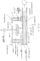
- Fig. 1 is a cross-sectional view illustrating a microwave-plasma processing apparatus disclosed in Japanese Patent Laying Open, Kokai Heisei 6-104098 filed by the common applicant to this application.
- the invention aimed to realize control of generation of a plasma and acceleration of ions in the plasma independently.
- a numeral reference "11" represents a reaction vessel, which is made of metal such as stainless steel, aluminum, or the like.
- the reaction vessel 11 has a periphery wall of double structure forming a coolant path 12.
- coolant circulates from a coolant inlet 12a to a coolant outlet 12b.
- a reaction chamber 13 is formed in the reaction vessel 11.
- the reaction vessel 11 is sealed at the top with a microwave introducing window 14, which is made of dielectric material, such as quartz glass, Pyrex glass, alumina, etc., having a low dielectric loss and heat resistance.
- a microwave introducing window 14 which is made of dielectric material, such as quartz glass, Pyrex glass, alumina, etc., having a low dielectric loss and heat resistance.
- an electric heater for heating the interior of the reaction chamber 13, an electric heater, not shown in Fig. 1, is provided around the reaction vessel 11. Both by heating with the electric heater and cooling with the coolant circulating in the coolant path 12, the inside the reaction chamber 13 is controlled in temperature precisely.
- the microwave introducing window 14 is provided on the lower surface with a conductive plate 31 of metal acting as a grounded electrode.
- the conductive plate 31 is provided with a plurality of microwave transmission openings 32, arranged perpendicularly to the direction of traveling of microwaves.
- the conductive plate 31 is grounded (33) through the reaction vessel 11.
- the conductive plate 31 may be placed in the middle between the microwave introducing window 14 and an object holder 15a, while the conductive plate 31 is grounded (33) through the reaction vessel 11, although the arrangement is not shown.
- the object holder 15a holding an object 30 to be processed is placed on a stage 15, which moves up and down by a driver (not shown).
- the object holder 15a is connected to a high-frequency power supply 18 to generate bias voltage on the surface of the object 30.
- the object holder 15a is provided with a chucking mechanism (not shown), such as an electrostatic chuck to hold the object 30 firmly.
- the object holder 15a is also provided with a cooling mechanism (not shown) in which coolant circulates for cooling the object 30.
- a gas outlet 16 connected to an exhaust apparatus (not shown) is formed on the bottom of the reaction vessel 11.
- a gas inlet 17 is formed to introduce predetermined reaction gas into the reaction chamber 13.
- the end of the dielectric line 21 is sealed with a reflecting plate 21b of metal.
- the dielectric layer 21c is attached on the lower surface of the metal plate 21a.
- the dielectric layer 21c is made of fluorine resin, polyethylene, polystyrene, or the like, having a low dielectric loss.
- the dielectric line 21 is connected through a waveguide 22 to a microwave oscillator 23, so that microwaves generated by the microwave oscillator 23 travel through the waveguide 22 into the dielectric line 21.
- the position of the stage 15 is adjusted in height so that the object 30 is placed at the appropriate position.
- unnecessary gases are discharged from the reaction chamber 13 through the gas outlet 16, then the reaction gas is introduced from the gas inlet 17 into the reaction chamber 13 until the pressure thereof reaches a predetermined level.
- the coolant is introduced from the coolant inlet 12a into the coolant path 12, and is discharged from the coolant outlet 12b.
- microwaves generated by the microwave oscillator 23 travels along the waveguide 22 to the dielectric line 21.
- the grounded potential is stable relative to the plasma, because the conductive plate 31 with the microwave transmission openings 32 are contacted on the microwave introducing window 14.
- the plasma potential becomes stable in the reaction chamber 13, and therefore, the stable bias voltage can be applied to the surface of the object 30 uniformly. Consequently, ion energy in the plasma can be well controlled, and the ions can be irradiated to the surface of the object vertically.
- the microwave introducing window 14 expands with the passage of time, when the apparatus keeps operating for a long time, so that an undesirable gap is formed between the conductive plate 31 and the microwave introducing window 14 because of a difference of thermal coefficient of expansion between them. As a result, undesirable electrical discharge may occur within the gap, and it becomes difficult to generate stable bias voltage on the object 30.
- the microwave introducing window 14 is eroded with plasma, because the microwave introducing window 14 is directly applied with plasma.
- the microwave introducing window 14 made of quartz glass, or the like is easily eroded with the halogen series of gas plasma, such as chlorine, fluorine and bromine.
- the microwave introducing window 14 is changed in width with the passage of time. Therefore, the density and distribution of plasma changes, and it becomes difficult to carry out plasma processing uniformly and stably.
- an object of the invention is to provide a plasma processing apparatus in which generation of undesirable electrical discharge can be avoided, so that stable bias voltage is uniformly applied to the surface of an object to be processed.
- Another object of the invention is to provide a plasma processing apparatus in which a microwave introducing window is protected from erosion.
- a plasma processing apparatus includes a conductive thin film provided on a surface of a microwave introducing member which is exposed to a processing chamber, in which an object to be processed is placed.
- the conductive thin film is provided at the entire portion excluding a transmission portion, through which microwaves pass into the processing chamber.
- the conductive thin film is grounded to act as an electrode.
- the conductive thin film is preferably be formed on the microwave introducing member by plasma sputtering technique.
- the conductive thin film may be mainly made of material selected from SiC, Si, C and Al to have a thickness of 10 ⁇ n to 100 ⁇ m.
- a plasma processing apparatus includes an insulation thin film provided on a surface of a microwave introducing member which is exposed to a processing chamber, in which an object to be processed is placed; and a conductive thin film provided on the entire surface of the microwave introducing member, excluding a transmission portion.
- the conductive thin film is grounded to act as an electrode.
- the insulation thin film is mainly made of inorganic oxide material or inorganic nitride material to have a thickness of 10 ⁇ m to 100 ⁇ m by plasma sputtering technique.
- the conductive thin film may be provided on the insulation thin film.
- the insulation thin film may be provided only at the transmission portion.
- the insulation thin film is provided at the transmission portion and over the conductive thin film.
- Fig. 1 is a cross-sectional view illustrating a conventional microwave-plasma processing apparatus.
- Fig. 2 is a cross-sectional view illustrating a microwave-plasma processing apparatus of a first preferred embodiment according to the invention.
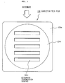
- Fig. 3 is a plan view showing a conductive thin film used in the first preferred embodiment shown in Fig. 2.
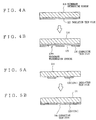
- Figs. 4A and 4B are cross-sectional views showing fabrication steps of a microwave introducing window with insulation thin film and conductive thin film, according to a second preferred embodiment of the invention.
- Figs. 5A and 5B are cross-sectional views showing fabrication steps of a microwave introducing window with insulation thin film and conductive thin film, according to a third preferred embodiment of the invention.
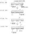
- Figs. 6A and 6B are cross-sectional views showing fabrication steps of a microwave introducing window with insulation thin film and conductive thin film, according to a fourth preferred embodiment of the invention.
- Figs. 7A and 7B are cross-sectional views showing fabrication steps of a microwave introducing window with insulation thin film and conductive thin film, according to a fifth preferred embodiment of the invention.
- Fig. 2 is a cross-sectional view illustrating a microwave-plasma processing apparatus of a first preferred embodiment according to the invention.
- a numeral reference "111" represents a reaction vessel, which is made of metal such as stainless steel, aluminum, or the like.
- the reaction vessel 111 has a periphery wall of double structure forming a coolant path 112. Along the coolant path 112, coolant circulates from a coolant inlet 112a to a coolant outlet 112b.
- a reaction chamber 113 is formed in the reaction vessel 111.
- the reaction vessel 111 is sealed at the top with a microwave introducing window 114, which is made of dielectric material, such as quartz glass, Pyrex glass, alumina, etc., having a low dielectric loss and heat resistance.
- a microwave introducing window 114 which is made of dielectric material, such as quartz glass, Pyrex glass, alumina, etc., having a low dielectric loss and heat resistance.
- an electric heater for heating the interior of the reaction chamber 113, an electric heater, not shown in Fig. 2, is provided around the reaction vessel 111. Both by heating with the electric heater and cooling with the coolant circulating in the coolant path 112, the inside the reaction chamber 113 is controlled in temperature precisely.
- the microwave introducing window 114 is selectively provided on the lower surface with a conductive thin film 124 functioning as a grounded electrode.
- the conductive thin film 124 is provided with a plurality of microwave transmission openings 124c, arranged perpendicularly to the direction of traveling of microwaves.
- the conductive thin film 124 is grounded (133) through the reaction vessel 111.
- the object holder 115a holding an object 130 to be processed is placed on a stage 115.
- the stage 115 is designed so as to move up and down by a driver (not shown).
- the object holder 115a is connected to a high-frequency power supply 118 to generate bias voltage on the surface of the object 130.
- the object holder 115a is provided at the top with a chucking mechanism (not shown), such as an electrostatic chuck to hold the object 130 firmly.
- the object holder 115a is also provided with a cooling mechanism (not shown) in which coolant circulates for cooling the object 130.
- a gas outlet 116 connected to an exhaust apparatus (not shown) is provided on the bottom of the reaction vessel 111.
- a gas inlet 117 is formed to introduce predetermined reaction gas into the reaction chamber 113.
- a dielectric line 121 composed of a metal plate 121a of aluminum, or the like, and a dielectric layer 121c.
- the end of the dielectric line 121 is sealed with a reflecting plate 121b of metal.
- the dielectric layer 121c is attached on the lower surface of the metal plate 121a.
- the dielectric layer 121c is made of fluorine resin, polyethylene, polystyrene, or the like, having a low dielectric loss.
- the dielectric line 121 is connected through a waveguide 122 to a microwave oscillator 123, so that microwaves generated by the microwave oscillator 123 travel through the waveguide 122 to the dielectric line 121.
- the position of the stage 115 is adjusted in height so that the object 130 is placed at the appropriate position.
- unnecessary gases are discharged from the reaction chamber 113 through the gas outlet 116, then the reaction gas is introduced from the gas inlet 117 into the reaction chamber 113 until the pressure thereof reaches a predetermined level.
- the coolant is introduced from the coolant inlet 112a into the coolant path 112, and is discharged from the coolant outlet 112b.
- microwaves generated by the microwave oscillator 123 travel along the waveguide 122 to the dielectric line 121.
- the microwaves When the microwaves are introduced in the dielectric line 121, electromagnetic field is generated under the dielectric line 121, and the microwaves pass through the microwave transmission openings 124c into the reaction chamber 113. In response to the microwaves, a plasma is generated in the reaction chamber 113. After that, when high-frequency voltage is applied from the high-frequency power supply 118 to the object holder 115a, the bias voltage is generated on the surface of the object 130. With the stable bias voltage, ions in the plasma are irradiated vertically to the surface of the object 130, while the energy of the ions is controlled. The object 130 is etched with the plasma in the reaction chamber 113.
- the conductive thin film 124 is entirely formed on the lower surface of the microwave introducing window 114 excluding the microwave transmission openings 124c by plasma sputtering technique.
- a numeral reference “124a” represents a contact portion being in contact with the reaction vessel 111
- "124b” represents a portion corresponding to the upper opening of the reaction chamber 113.
- the microwaves pass through the microwave transmission openings 124c into the reaction chamber 113.
- the conductive thin film 124 is electrically in contact with the reaction vessel 111 which is grounded, so that the conductive thin film 124 functions as a grounded electrode.
- the portion corresponding to the openings 124c are covered with a masking tape.
- the conductive thin film 124 is made of material having conductivity and high corrosion resistance to the halogen series of gas plasma, and not producing contaminants.
- material having conductivity and high corrosion resistance to the halogen series of gas plasma for instance, SiC, Si, C, Al or a kind of material having a thin oxidized layer, such as aluminum covered on the surface with an alumite layer.
- the conductive thin film 124 is preferably formed to have a thickness of 10 to 100 ⁇ m. If the thickness of the film 124 is less than 10 ⁇ m, the thin film 124 has inferior heat resistance and inferior plasma resistance. On the other hand, if the thickness of the conductive thin film 124 is more than 100 ⁇ m, the cost of formation thereof becomes high and the thin film 124 has low density, causing cracking and peeling thereof.
- microwave transmission openings 124c are not limited in shape, those are preferably shaped into rectangular slits as shown in Fig. 3.
- CVD Chemical Vapor Deposition
- LTAVD Low Temperature Arc Vapor Deposition
- sputtering technique is preferable, and any kinds of sputtering technique are applicable.
- conductive thin film 124 has characteristics of a low p.p.b. level of impurity; high corrosion resistance; high strength; high density; high heat resistance; high degree of adhesion to the microwave introducing window 114; high applicability of being coated on complicated shape of products; high applicability of changing the thickness; high crystal directivity for crystal metal, etc. Therefore, the conductive thin film 124 of the invention are suited for covering the microwave introducing window 114.
- a microwave introducing window 114 is provided on the lower surface facing the object holder 115a with a conductive thin film (134, 144, 154, 164) and an insulation thin film (125, 135, 155, 165).
- the combination of the conductive thin film and the insulation thin film is different from each other among the second to fifth preferred embodiments.
- FIGs. 4A and 4B are enlarged cross-sectional views illustrating the fabrication steps of a microwave introducing window 114 employed in a microwave-plasma processing apparatus of the second preferred embodiment.
- Figs. 4A and 4B only the microwave introducing window 114 is partly shown, because the other components of the apparatus are the same as those in the first preferred embodiment.
- an insulation thin film 125 is formed entirely on the lower surface of the microwave introducing window 114 facing the object holder 115a, as shown in Fig. 4A.
- the insulation thin film 125 is preferably made of material having high corrosion resistance and not contaminating easily. For instance, inorganic oxide material such as alumina (Al 2 O 3 ) and yttrium (Y 2 O 5 ), and inorganic nitride material such as silicon nitride (SiN) and boron nitride (BN) are applicable.
- the insulation thin film 125 can be formed in the same manner as the conductive thin film 124 shown in Figs. 2 and 3.
- the insulation thin film 125 is preferably formed to have a thickness of 10 to 100 ⁇ m. If the thickness of the insulation thin film 125 is less than 10 ⁇ m, the thin film 125 has inferior heat resistance and inferior plasma resistance.
- insulation thin film 125 has the same advantageous characteristics as the above mentioned conductive thin film 124.
- a conductive thin film 134 is formed on the insulation thin film 125 in the same manner as that in the first preferred embodiment.
- the conductive thin film 134 has the same thickness and shape as those of the conductive thin film 124 of the first preferred embodiment.
- the insulation thin film 125 is formed throughout on the lower surface of the microwave introducing window 114, and the conductive thin film 134 is selectively formed on the insulation thin film 125 having the same shape as the conductive thin film 124 shown in Fig. 3.
- microwaves pass through the portion, where the insulation thin film 125 is only formed, into the reaction chamber 113.
- FIGs. 5A and 5B are enlarged cross-sectional views illustrating the fabrication steps of a microwave introducing window 114 employed in a microwave-plasma processing apparatus of the third preferred embodiment.
- Figs. 5A and 5B only the microwave introducing window 114 is partly shown, because the other components of the apparatus are the same as those in the first preferred embodiment.
- an insulation thin film 135 is formed selectively on the lower surface of the microwave introducing window 114. Then, a conductive thin film 144 is formed at the remaining portion on the microwave introducing window 114. The portion at which the insulation thin film 135 is formed becomes the microwave transmission openings 124c shown in Fig. 3.
- the lower surface of the microwave introducing window 114 excluding the microwave transmission openings 124c is covered with a masking tape, then the insulation thin film 135 is formed by sputtering technique at the portion for the microwave transmission openings 124c.
- the insulation thin film 135 is covered with a masking tape, then the conductive thin film 144 is formed at the remaining portion.
- the insulation thin film 135 and conductive thin film 144 are preferably formed to have the same thickness.
- the insulation thin film 135 is formed only on the portion for the microwave transmission openings 124c, and the conductive thin film 144 is formed on the remaining portion on the lower surface of the microwave introducing window 114.
- microwaves pass through the microwave transmission openings 124c, on which the insulation thin film 135 is formed, into the reaction chamber 113.
- FIGs. 6A and 6B are enlarged cross-sectional views illustrating the fabrication steps of a microwave introducing window 114 employed in a microwave-plasma processing apparatus of the fourth preferred embodiment.
- Figs. 6A and 6B only the microwave introducing window 114 is partly shown, because the other components of the apparatus are the same as those in the first preferred embodiment.
- a conductive thin film 154 is selectively formed on the lower surface of the microwave introducing window 114 in the same manner as the first preferred embodiment. Then, an insulation thin film 155 is formed over the entire surface, corresponding to the upper opening (124b in Fig. 3) of the microwave introducing window 114, including the portion for the microwave transmission openings 124c.
- the conductive thin film 154 is first covered with a masking tape, then the insulation thin film 155 is formed at the portion for the microwave transmission openings 124c to have the same thickness as the conductive thin film 154. After that, the masking tape on the opening 124b is removed, and the insulation thin film 155 is formed again on the entire surface.
- the insulation thin film 155 is not formed on the contact portion 124a, shown in Fig. 3, because the portion 124a is to be grounded though the reaction vessel 111.
- the conductive thin film 154 is only formed.
- the insulation thin film 155 is formed on the conductive thin film 154 and on the portion for the microwave transmission openings 124c to have a flat surface.
- the thickness of the insulation thin film 155 is preferably 20 to 200 ⁇ m.
- the contact portion 124a is provided at the surface only with the conductive thin film 154, so that the conductive thin film 154 is grounded through the reaction vessel 111.
- the microwave transmission openings 124c are provided at the inside only with the insulation thin film 155, so that microwaves pass through them into the reaction chamber 113.
- FIGs. 7A and 7B are enlarged cross-sectional views illustrating the fabrication steps of a microwave introducing window 114 employed in a microwave-plasma processing apparatus of the fifth preferred embodiment.
- Figs. 7A and 7B only the microwave introducing window 114 is partly shown, because the other components of the apparatus are the same as those in the first preferred embodiment.
- a conductive thin film 164 is selectively formed on the lower surface of the microwave introducing window 114 in the same manner as the first preferred embodiment. Then, an insulation thin film 165 is formed over the entire surface, corresponding to the upper opening of the microwave introducing window 114 (shown as the portion "124b" in Fig. 3), including the portion for the microwave transmission openings 124c.
- the insulation thin film 165 is first covered with a masking tape, then the insulation thin film 165 is formed at the portion for the microwave transmission openings 124c to have the same thickness as the conductive thin film 164. After that, the masking tape on the opening 124b is removed, and the portion for the microwave transmission openings 124c are covered with a masking tape, then the insulation thin film 165 is again formed as shown in Fig. 7B.
- the conductive thin film 164 is formed in the same manner as the first preferred embodiment, as shown in Fig. 7A, then the insulation thin film 165 is formed on the upper opening 124b of the microwave introducing window 114 including the portion for the microwave transmission openings 124c.
- the contact portion 124a is covered with masking tape, then the insulation thin film 165 is formed on the upper opening 124b and the microwave transmission openings 124c simultaneously.
- the conductive thin film 164 is only formed.
- the insulation thin film 165 is formed on the conductive thin film 164 formed on the upper opening 124a excluding the microwave transmission openings 124c, and on the portion for the microwave transmission openings 124c.
- the thicknesses of the thin films are different between the portion on which only the insulation thin film 165 is formed and the portion on which both the conductive thin film 164 and the insulation thin film 165 are formed.
- the insulation thin film 165 at the microwave transmission openings 124c has the same thickness as the conductive thin film 164.
- the additional insulation thin film 165 is formed to have a thickness of 10 to 100 ⁇ m.
- the contact portion 124a is provided only with the conductive thin film 164, so that the conductive thin film 164 is grounded through the reaction vessel 111.
- the microwave transmission openings 124c are provided at the inside only with the insulation thin film 165, so that microwaves pass through them into the reaction chamber 113.
- Test 1 was carried out for the microwave-plasma processing apparatus of the first preferred embodiment shown in Figs. 2 and 3.
- the conductive thin film 124 is formed by plasma sputtering technique with target material of aluminum in an atmosphere of Ar gas to have a thickness of 50 ⁇ m, and each of the microwave transmission openings 124c is shaped to be a rectangle of 200mm ⁇ 30mm.
- a mean value of etching speed of a SiO 2 layer is examined. The etching process is performed pursuant to the conditions as follows:
- a mean value of etching speed of the SiO 2 layers is 600nm/minute, and a uniformity of the etching speed of the tested silicon wafers is ⁇ 5%.
- etching speed and its uniformity is examined to the last ten wafers.
- a mean value of etching speed is 590nm/minute and a uniformity of the etching speed is ⁇ 5%.
- Test 2 was carried out for the microwave-plasma processing apparatus of the fourth preferred embodiment shown in Figs. 6A and 6B.
- the conductive thin film 154 of aluminum is formed in the same manner as Test 1 to have a thickness of 50 ⁇ m.
- the insulation thin film 155 is formed by plasma sputtering technique with target material of Al 2 O 3 in an atmosphere of Ar gas to have a thickness of 50 ⁇ m.
- Each of the microwave transmission openings 124c is shaped to be a rectangle of 200mm ⁇ 30mm.
- a mean value of etching speed of a SiO 2 layer is examined. The etching process is performed pursuant to the conditions as follows:
- a mean value of etching speed of the SiO 2 layers is 680nm/minute, and a uniformity of the etching speed of the tested silicon wafers is ⁇ 5%.
- etching speed and its uniformity is examined to the last ten wafers.
- a mean value of etching speed is 570nm/minute and a uniformity of the etching speed is ⁇ 5%.
- the conventional apparatus includes the same components as the apparatus of the invention shown in Fig. 2 except that the microwave introducing window 14 is provided with the conductive plate 31.
- the conductive plate 31 is not attached on the microwave introducing window 14, but contacted on it.
- the test is performed in the same condition of Test 1.
- a mean value of etching speed of the SiO 2 layers is 600nm/minute, and a uniformity of the etching speed of the tested silicon wafers is ⁇ 5%.
- an undesirable gap is formed between the conductive plate 31 and the microwave introducing window 14.
- the microwave introducing window 114 is covered on the lower surface with the conductive thin film 124, so that it can be prevented that a gap is formed between the microwave introducing window 114 and the conductive thin film 114 (electrode), even if the apparatus operates long.
- the conductive thin film 124 is grounded, and the object holder 115a is applied with high-frequency voltage. As a result, no undesirable electric discharge occurs in the reaction chamber 113, and therefore, stable bias voltage can be applied to the surface of the object 130. Consequently, as understood from the results of the tests, the objects such as silicon wafers can be uniformly etched at a stable speed for a long time.
- the microwave introducing window 114 is covered at the opening portion (124b) with the insulation thin film 155 entirely including the portion on which the conductive thin film 154 is formed.
- the conductive thin film 154 is grounded, and the object holder 115a is applied with high-frequency voltage.
- the microwave introducing window 114 is not eroded with plasma. That is, the objects such as silicon wafers can be uniformly etched at a stable speed for a long time.
Abstract
Description
- The present invention relates to a plasma processing apparatus, and more particularly to a microwave-plasma processing apparatus for etching semiconductor wafers, or for forming thin films on the wafers.
- In fabrication of highly integrated semiconductor devices, microwave-plasma processing apparatuses have been widely used. In such a microwave-plasma processing apparatus, reaction gases and microwaves are introduced into a vacuum chamber to generate gas-discharge, so that a plasma is produced in the chamber. The plasma is applied to a substrate to etch the surface thereof, or to form thin film layers thereon. Especially, in dry-etching technology and embedding technology, microwave-plasma processing apparatuses controlling generation of the plasma and acceleration of ions in the plasma independently have become important and been studied extensively.
- Fig. 1 is a cross-sectional view illustrating a microwave-plasma processing apparatus disclosed in Japanese Patent Laying Open, Kokai Heisei 6-104098 filed by the common applicant to this application. The invention aimed to realize control of generation of a plasma and acceleration of ions in the plasma independently. In Fig. 1, a numeral reference "11" represents a reaction vessel, which is made of metal such as stainless steel, aluminum, or the like. The
reaction vessel 11 has a periphery wall of double structure forming acoolant path 12. Along thecoolant path 12, coolant circulates from acoolant inlet 12a to acoolant outlet 12b. Areaction chamber 13 is formed in thereaction vessel 11. Thereaction vessel 11 is sealed at the top with amicrowave introducing window 14, which is made of dielectric material, such as quartz glass, Pyrex glass, alumina, etc., having a low dielectric loss and heat resistance. For heating the interior of thereaction chamber 13, an electric heater, not shown in Fig. 1, is provided around thereaction vessel 11. Both by heating with the electric heater and cooling with the coolant circulating in thecoolant path 12, the inside thereaction chamber 13 is controlled in temperature precisely. - The
microwave introducing window 14 is provided on the lower surface with aconductive plate 31 of metal acting as a grounded electrode. Theconductive plate 31 is provided with a plurality ofmicrowave transmission openings 32, arranged perpendicularly to the direction of traveling of microwaves. Theconductive plate 31 is grounded (33) through thereaction vessel 11. Theconductive plate 31 may be placed in the middle between themicrowave introducing window 14 and anobject holder 15a, while theconductive plate 31 is grounded (33) through thereaction vessel 11, although the arrangement is not shown. - In the
reaction chamber 13, theobject holder 15a holding anobject 30 to be processed is placed on astage 15, which moves up and down by a driver (not shown). Theobject holder 15a is connected to a high-frequency power supply 18 to generate bias voltage on the surface of theobject 30. Theobject holder 15a is provided with a chucking mechanism (not shown), such as an electrostatic chuck to hold theobject 30 firmly. Theobject holder 15a is also provided with a cooling mechanism (not shown) in which coolant circulates for cooling theobject 30. On the bottom of thereaction vessel 11, agas outlet 16 connected to an exhaust apparatus (not shown) is formed. On the side wall of thereaction vessel 11, agas inlet 17 is formed to introduce predetermined reaction gas into thereaction chamber 13. - Over the
reaction vessel 11, adielectric line 21, composed of ametal plate 21a of aluminum, or the like, and adielectric layer 21c, is provided. The end of thedielectric line 21 is sealed with a reflecting plate 21b of metal. Thedielectric layer 21c is attached on the lower surface of themetal plate 21a. Thedielectric layer 21c is made of fluorine resin, polyethylene, polystyrene, or the like, having a low dielectric loss. Thedielectric line 21 is connected through awaveguide 22 to amicrowave oscillator 23, so that microwaves generated by themicrowave oscillator 23 travel through thewaveguide 22 into thedielectric line 21. - In the above mentioned microwave-plasma processing apparatus, for etching the surface of the
object 30 held by theobject holder 15a, the position of thestage 15 is adjusted in height so that theobject 30 is placed at the appropriate position. Next, unnecessary gases are discharged from thereaction chamber 13 through thegas outlet 16, then the reaction gas is introduced from thegas inlet 17 into thereaction chamber 13 until the pressure thereof reaches a predetermined level. At the same time, the coolant is introduced from thecoolant inlet 12a into thecoolant path 12, and is discharged from thecoolant outlet 12b. Subsequently, microwaves generated by themicrowave oscillator 23 travels along thewaveguide 22 to thedielectric line 21. When the microwaves are introduced in thedielectric line 21, electromagnetic field is generated under thedielectric line 21, and the microwaves pass through themicrowave transmission openings 32 into thereaction chamber 13. In response to the microwaves, a plasma is generated in thereaction chamber 13. After that, when high-frequency voltage is applied from the high-frequency power supply 18 to theobject holder 15a, bias voltage is generated on the surface of theobject 30. With the stable bias voltage, ions in the plasma are irradiated vertically to the surface of theobject 30 to be etched, while the energy of the ions is controlled. - In the microwave-plasma processing apparatus, the grounded potential is stable relative to the plasma, because the
conductive plate 31 with themicrowave transmission openings 32 are contacted on themicrowave introducing window 14. As a result, the plasma potential becomes stable in thereaction chamber 13, and therefore, the stable bias voltage can be applied to the surface of theobject 30 uniformly. Consequently, ion energy in the plasma can be well controlled, and the ions can be irradiated to the surface of the object vertically. - According to the conventional microwave-plasma processing apparatus, however, the
microwave introducing window 14 expands with the passage of time, when the apparatus keeps operating for a long time, so that an undesirable gap is formed between theconductive plate 31 and themicrowave introducing window 14 because of a difference of thermal coefficient of expansion between them. As a result, undesirable electrical discharge may occur within the gap, and it becomes difficult to generate stable bias voltage on theobject 30. - There is another disadvantage in that the
microwave introducing window 14 is eroded with plasma, because themicrowave introducing window 14 is directly applied with plasma. Especially, themicrowave introducing window 14 made of quartz glass, or the like is easily eroded with the halogen series of gas plasma, such as chlorine, fluorine and bromine. As a result, themicrowave introducing window 14 is changed in width with the passage of time. Therefore, the density and distribution of plasma changes, and it becomes difficult to carry out plasma processing uniformly and stably. - Accordingly, an object of the invention is to provide a plasma processing apparatus in which generation of undesirable electrical discharge can be avoided, so that stable bias voltage is uniformly applied to the surface of an object to be processed.
- Another object of the invention is to provide a plasma processing apparatus in which a microwave introducing window is protected from erosion.
- Additional objects, advantages and novel features of the invention will be set forth in part in the description that follows, and in part will become apparent to those skilled in the art upon examination of the following or may be learned by practice of the invention. The objects and advantages of the invention may be realized and attained by means of the instrumentalities and combinations particularly pointed out in the appended claims.
- According to a first aspect of the invention, a plasma processing apparatus includes a conductive thin film provided on a surface of a microwave introducing member which is exposed to a processing chamber, in which an object to be processed is placed. The conductive thin film is provided at the entire portion excluding a transmission portion, through which microwaves pass into the processing chamber. The conductive thin film is grounded to act as an electrode. In the apparatus, the conductive thin film is preferably be formed on the microwave introducing member by plasma sputtering technique. The conductive thin film may be mainly made of material selected from SiC, Si, C and Al to have a thickness of 10µn to 100µm.
- According to a second aspect of the invention, a plasma processing apparatus includes an insulation thin film provided on a surface of a microwave introducing member which is exposed to a processing chamber, in which an object to be processed is placed; and a conductive thin film provided on the entire surface of the microwave introducing member, excluding a transmission portion. The conductive thin film is grounded to act as an electrode. In the apparatus, preferably, the insulation thin film is mainly made of inorganic oxide material or inorganic nitride material to have a thickness of 10µm to 100µm by plasma sputtering technique. The conductive thin film may be provided on the insulation thin film. The insulation thin film may be provided only at the transmission portion. The insulation thin film is provided at the transmission portion and over the conductive thin film.
- Fig. 1 is a cross-sectional view illustrating a conventional microwave-plasma processing apparatus.
- Fig. 2 is a cross-sectional view illustrating a microwave-plasma processing apparatus of a first preferred embodiment according to the invention.
- Fig. 3 is a plan view showing a conductive thin film used in the first preferred embodiment shown in Fig. 2.
- Figs. 4A and 4B are cross-sectional views showing fabrication steps of a microwave introducing window with insulation thin film and conductive thin film, according to a second preferred embodiment of the invention.
- Figs. 5A and 5B are cross-sectional views showing fabrication steps of a microwave introducing window with insulation thin film and conductive thin film, according to a third preferred embodiment of the invention.
- Figs. 6A and 6B are cross-sectional views showing fabrication steps of a microwave introducing window with insulation thin film and conductive thin film, according to a fourth preferred embodiment of the invention.
- Figs. 7A and 7B are cross-sectional views showing fabrication steps of a microwave introducing window with insulation thin film and conductive thin film, according to a fifth preferred embodiment of the invention.
- Fig. 2 is a cross-sectional view illustrating a microwave-plasma processing apparatus of a first preferred embodiment according to the invention. In Fig. 2, a numeral reference "111" represents a reaction vessel, which is made of metal such as stainless steel, aluminum, or the like. The
reaction vessel 111 has a periphery wall of double structure forming acoolant path 112. Along thecoolant path 112, coolant circulates from acoolant inlet 112a to acoolant outlet 112b. Areaction chamber 113 is formed in thereaction vessel 111. Thereaction vessel 111 is sealed at the top with amicrowave introducing window 114, which is made of dielectric material, such as quartz glass, Pyrex glass, alumina, etc., having a low dielectric loss and heat resistance. For heating the interior of thereaction chamber 113, an electric heater, not shown in Fig. 2, is provided around thereaction vessel 111. Both by heating with the electric heater and cooling with the coolant circulating in thecoolant path 112, the inside thereaction chamber 113 is controlled in temperature precisely. - The
microwave introducing window 114 is selectively provided on the lower surface with a conductivethin film 124 functioning as a grounded electrode. The conductivethin film 124 is provided with a plurality ofmicrowave transmission openings 124c, arranged perpendicularly to the direction of traveling of microwaves. The conductivethin film 124 is grounded (133) through thereaction vessel 111. - In the
reaction chamber 113, theobject holder 115a holding anobject 130 to be processed is placed on astage 115. Thestage 115 is designed so as to move up and down by a driver (not shown). Theobject holder 115a is connected to a high-frequency power supply 118 to generate bias voltage on the surface of theobject 130. Theobject holder 115a is provided at the top with a chucking mechanism (not shown), such as an electrostatic chuck to hold theobject 130 firmly. Theobject holder 115a is also provided with a cooling mechanism (not shown) in which coolant circulates for cooling theobject 130. On the bottom of thereaction vessel 111, agas outlet 116 connected to an exhaust apparatus (not shown) is provided. On the side wall of thereaction vessel 111, agas inlet 117 is formed to introduce predetermined reaction gas into thereaction chamber 113. - Over the
reaction vessel 111, adielectric line 121, composed of ametal plate 121a of aluminum, or the like, and adielectric layer 121c, is provided. The end of thedielectric line 121 is sealed with a reflectingplate 121b of metal. Thedielectric layer 121c is attached on the lower surface of themetal plate 121a. Thedielectric layer 121c is made of fluorine resin, polyethylene, polystyrene, or the like, having a low dielectric loss. Thedielectric line 121 is connected through awaveguide 122 to amicrowave oscillator 123, so that microwaves generated by themicrowave oscillator 123 travel through thewaveguide 122 to thedielectric line 121. - In the above mentioned microwave-plasma processing apparatus, for etching the surface of the
object 130 held by theobject holder 115a, the position of thestage 115 is adjusted in height so that theobject 130 is placed at the appropriate position. Next, unnecessary gases are discharged from thereaction chamber 113 through thegas outlet 116, then the reaction gas is introduced from thegas inlet 117 into thereaction chamber 113 until the pressure thereof reaches a predetermined level. At the same time, the coolant is introduced from thecoolant inlet 112a into thecoolant path 112, and is discharged from thecoolant outlet 112b. Subsequently, microwaves generated by themicrowave oscillator 123 travel along thewaveguide 122 to thedielectric line 121. When the microwaves are introduced in thedielectric line 121, electromagnetic field is generated under thedielectric line 121, and the microwaves pass through themicrowave transmission openings 124c into thereaction chamber 113. In response to the microwaves, a plasma is generated in thereaction chamber 113. After that, when high-frequency voltage is applied from the high-frequency power supply 118 to theobject holder 115a, the bias voltage is generated on the surface of theobject 130. With the stable bias voltage, ions in the plasma are irradiated vertically to the surface of theobject 130, while the energy of the ions is controlled. Theobject 130 is etched with the plasma in thereaction chamber 113. - Next, the detail of the
microwave introducing window 114 with the conductivethin film 124 is now described in conjunction with Fig. 3. The conductivethin film 124 is entirely formed on the lower surface of themicrowave introducing window 114 excluding themicrowave transmission openings 124c by plasma sputtering technique. In Fig. 3, a numeral reference "124a" represents a contact portion being in contact with thereaction vessel 111, and "124b" represents a portion corresponding to the upper opening of thereaction chamber 113. The microwaves pass through themicrowave transmission openings 124c into thereaction chamber 113. The conductivethin film 124 is electrically in contact with thereaction vessel 111 which is grounded, so that the conductivethin film 124 functions as a grounded electrode. For forming the conductivethin film 124, the portion corresponding to theopenings 124c are covered with a masking tape. - Preferably, the conductive
thin film 124 is made of material having conductivity and high corrosion resistance to the halogen series of gas plasma, and not producing contaminants. For instance, SiC, Si, C, Al or a kind of material having a thin oxidized layer, such as aluminum covered on the surface with an alumite layer. For heat resistance and plasma resistance characteristics and the cost of fabrication, the conductivethin film 124 is preferably formed to have a thickness of 10 to 100µm. If the thickness of thefilm 124 is less than 10µm, thethin film 124 has inferior heat resistance and inferior plasma resistance. On the other hand, if the thickness of the conductivethin film 124 is more than 100µm, the cost of formation thereof becomes high and thethin film 124 has low density, causing cracking and peeling thereof. - Although the
microwave transmission openings 124c are not limited in shape, those are preferably shaped into rectangular slits as shown in Fig. 3. - For forming the conductive
thin film 124 on the lower surface of themicrowave introducing window 114, besides plasma sputtering technique described above, CVD (Chemical Vapor Deposition) technique, other types of sputtering technique, LTAVD (Low Temperature Arc Vapor Deposition) coating technique are applicable. In those variety kinds of technique, sputtering technique is preferable, and any kinds of sputtering technique are applicable. - Thus formed conductive
thin film 124 has characteristics of a low p.p.b. level of impurity; high corrosion resistance; high strength; high density; high heat resistance; high degree of adhesion to themicrowave introducing window 114; high applicability of being coated on complicated shape of products; high applicability of changing the thickness; high crystal directivity for crystal metal, etc. Therefore, the conductivethin film 124 of the invention are suited for covering themicrowave introducing window 114. - Second to fifth preferred embodiments of the invention are now described in conjunction with the appended drawings. In the second to fifth preferred embodiment, a
microwave introducing window 114 is provided on the lower surface facing theobject holder 115a with a conductive thin film (134, 144, 154, 164) and an insulation thin film (125, 135, 155, 165). The combination of the conductive thin film and the insulation thin film is different from each other among the second to fifth preferred embodiments. - First, a microwave-plasma processing apparatus of the second preferred embodiment is described. Figs. 4A and 4B are enlarged cross-sectional views illustrating the fabrication steps of a
microwave introducing window 114 employed in a microwave-plasma processing apparatus of the second preferred embodiment. In Figs. 4A and 4B, only themicrowave introducing window 114 is partly shown, because the other components of the apparatus are the same as those in the first preferred embodiment. - In fabrication, first of all, an insulation
thin film 125 is formed entirely on the lower surface of themicrowave introducing window 114 facing theobject holder 115a, as shown in Fig. 4A. - The insulation
thin film 125 is preferably made of material having high corrosion resistance and not contaminating easily. For instance, inorganic oxide material such as alumina (Al2O3) and yttrium (Y2O5), and inorganic nitride material such as silicon nitride (SiN) and boron nitride (BN) are applicable. The insulationthin film 125 can be formed in the same manner as the conductivethin film 124 shown in Figs. 2 and 3. The insulationthin film 125 is preferably formed to have a thickness of 10 to 100µm. If the thickness of the insulationthin film 125 is less than 10µm, thethin film 125 has inferior heat resistance and inferior plasma resistance. On the other hand, if the thickness of the insulationthin film 125 is more than 100µm, the cost of formation of thethin film 125 becomes high and thefilm 125 has low density, causing cracking and peeling thereof. Thus formed insulationthin film 125 has the same advantageous characteristics as the above mentioned conductivethin film 124. - Next, as shown in Fig. 4B, a conductive
thin film 134 is formed on the insulationthin film 125 in the same manner as that in the first preferred embodiment. The conductivethin film 134 has the same thickness and shape as those of the conductivethin film 124 of the first preferred embodiment. - Accordingly, it can be thought that the insulation
thin film 125 is formed throughout on the lower surface of themicrowave introducing window 114, and the conductivethin film 134 is selectively formed on the insulationthin film 125 having the same shape as the conductivethin film 124 shown in Fig. 3. As a result, microwaves pass through the portion, where the insulationthin film 125 is only formed, into thereaction chamber 113. - Next, a microwave-plasma processing apparatus of the third preferred embodiment is described. Figs. 5A and 5B are enlarged cross-sectional views illustrating the fabrication steps of a
microwave introducing window 114 employed in a microwave-plasma processing apparatus of the third preferred embodiment. In Figs. 5A and 5B, only themicrowave introducing window 114 is partly shown, because the other components of the apparatus are the same as those in the first preferred embodiment. - As shown in Fig. 5A, an insulation
thin film 135 is formed selectively on the lower surface of themicrowave introducing window 114. Then, a conductivethin film 144 is formed at the remaining portion on themicrowave introducing window 114. The portion at which the insulationthin film 135 is formed becomes themicrowave transmission openings 124c shown in Fig. 3. In practical fabrication, the lower surface of themicrowave introducing window 114 excluding themicrowave transmission openings 124c is covered with a masking tape, then the insulationthin film 135 is formed by sputtering technique at the portion for themicrowave transmission openings 124c. Next, the insulationthin film 135 is covered with a masking tape, then the conductivethin film 144 is formed at the remaining portion. The insulationthin film 135 and conductivethin film 144 are preferably formed to have the same thickness. - As described above, according to the third preferred embodiment, the insulation
thin film 135 is formed only on the portion for themicrowave transmission openings 124c, and the conductivethin film 144 is formed on the remaining portion on the lower surface of themicrowave introducing window 114. As a result, microwaves pass through themicrowave transmission openings 124c, on which the insulationthin film 135 is formed, into thereaction chamber 113. - Next, a microwave-plasma processing apparatus of the fourth preferred embodiment is described. Figs. 6A and 6B are enlarged cross-sectional views illustrating the fabrication steps of a
microwave introducing window 114 employed in a microwave-plasma processing apparatus of the fourth preferred embodiment. In Figs. 6A and 6B, only themicrowave introducing window 114 is partly shown, because the other components of the apparatus are the same as those in the first preferred embodiment. - As shown in Fig. 6A, a conductive
thin film 154 is selectively formed on the lower surface of themicrowave introducing window 114 in the same manner as the first preferred embodiment. Then, an insulationthin film 155 is formed over the entire surface, corresponding to the upper opening (124b in Fig. 3) of themicrowave introducing window 114, including the portion for themicrowave transmission openings 124c. For forming the insulationthin film 155, the conductivethin film 154 is first covered with a masking tape, then the insulationthin film 155 is formed at the portion for themicrowave transmission openings 124c to have the same thickness as the conductivethin film 154. After that, the masking tape on theopening 124b is removed, and the insulationthin film 155 is formed again on the entire surface. The insulationthin film 155, however, is not formed on thecontact portion 124a, shown in Fig. 3, because theportion 124a is to be grounded though thereaction vessel 111. - As described above, at the
contact portion 124a on the lower surface of themicrowave introducing window 114, the conductivethin film 154 is only formed. The insulationthin film 155 is formed on the conductivethin film 154 and on the portion for themicrowave transmission openings 124c to have a flat surface. The thickness of the insulationthin film 155 is preferably 20 to 200µm. - The
contact portion 124a is provided at the surface only with the conductivethin film 154, so that the conductivethin film 154 is grounded through thereaction vessel 111. On the other hand, themicrowave transmission openings 124c are provided at the inside only with the insulationthin film 155, so that microwaves pass through them into thereaction chamber 113. - Next, a microwave-plasma processing apparatus of the fifth preferred embodiment is described. Figs. 7A and 7B are enlarged cross-sectional views illustrating the fabrication steps of a
microwave introducing window 114 employed in a microwave-plasma processing apparatus of the fifth preferred embodiment. In Figs. 7A and 7B, only themicrowave introducing window 114 is partly shown, because the other components of the apparatus are the same as those in the first preferred embodiment. - As shown in Fig. 7A, a conductive
thin film 164 is selectively formed on the lower surface of themicrowave introducing window 114 in the same manner as the first preferred embodiment. Then, an insulationthin film 165 is formed over the entire surface, corresponding to the upper opening of the microwave introducing window 114 (shown as the portion "124b" in Fig. 3), including the portion for themicrowave transmission openings 124c. For forming the insulationthin film 165, the conductivethin film 164 is first covered with a masking tape, then the insulationthin film 165 is formed at the portion for themicrowave transmission openings 124c to have the same thickness as the conductivethin film 164. After that, the masking tape on theopening 124b is removed, and the portion for themicrowave transmission openings 124c are covered with a masking tape, then the insulationthin film 165 is again formed as shown in Fig. 7B. - For fabrication of the
microwave introducing window 114 of the fifth preferred embodiment, another method is applicable. According to the other method, the conductivethin film 164 is formed in the same manner as the first preferred embodiment, as shown in Fig. 7A, then the insulationthin film 165 is formed on theupper opening 124b of themicrowave introducing window 114 including the portion for themicrowave transmission openings 124c. For forming the insulationthin film 165, thecontact portion 124a is covered with masking tape, then the insulationthin film 165 is formed on theupper opening 124b and themicrowave transmission openings 124c simultaneously. - As described above, at the
contact portion 124a on the lower surface of themicrowave introducing window 114, the conductivethin film 164 is only formed. The insulationthin film 165 is formed on the conductivethin film 164 formed on theupper opening 124a excluding themicrowave transmission openings 124c, and on the portion for themicrowave transmission openings 124c. The thicknesses of the thin films are different between the portion on which only the insulationthin film 165 is formed and the portion on which both the conductivethin film 164 and the insulationthin film 165 are formed. In other words, the insulationthin film 165 at themicrowave transmission openings 124c has the same thickness as the conductivethin film 164. On the conductivethin film 164, the additional insulationthin film 165 is formed to have a thickness of 10 to 100µm. - The
contact portion 124a is provided only with the conductivethin film 164, so that the conductivethin film 164 is grounded through thereaction vessel 111. On the other hand, themicrowave transmission openings 124c are provided at the inside only with the insulationthin film 165, so that microwaves pass through them into thereaction chamber 113. - Next, experimental data for the present invention will be described.
- Test 1 was carried out for the microwave-plasma processing apparatus of the first preferred embodiment shown in Figs. 2 and 3. In test 1, the conductive
thin film 124 is formed by plasma sputtering technique with target material of aluminum in an atmosphere of Ar gas to have a thickness of 50µm, and each of themicrowave transmission openings 124c is shaped to be a rectangle of 200mm × 30mm. A mean value of etching speed of a SiO2 layer is examined. The etching process is performed pursuant to the conditions as follows: -
- Object (130):
- 8'' Silicon Wafer with 1µm of SiO2 layer
- Discharge Gas Mixture:
- CF4 of 30sccm
CHF3 of 30sccm
Ar of 100sccn - Pressure in Reaction Chamber (113):
- 30mTorr
- Microwave Frequency:
- 2.45GHz
- Power for generating Plasma:
- 1kW
- High-frequency (RF) to
Holder 115a, Frequency: - 400kHz, Power: 600W
- Number of Wafers to be tested:
- 10
- Time for Etching:
- 1 minute
- According to the test 1, a mean value of etching speed of the SiO2 layers is 600nm/minute, and a uniformity of the etching speed of the tested silicon wafers is ± 5%.
- After 500 pieces of silicon wafers are etched in the same condition, etching speed and its uniformity is examined to the last ten wafers. As a result, a mean value of etching speed is 590nm/minute and a uniformity of the etching speed is ±5%.
- Test 2 was carried out for the microwave-plasma processing apparatus of the fourth preferred embodiment shown in Figs. 6A and 6B. In test 2, the conductive
thin film 154 of aluminum is formed in the same manner as Test 1 to have a thickness of 50µm. The insulationthin film 155 is formed by plasma sputtering technique with target material of Al2O3 in an atmosphere of Ar gas to have a thickness of 50µm. Each of themicrowave transmission openings 124c is shaped to be a rectangle of 200mm × 30mm. A mean value of etching speed of a SiO2 layer is examined. The etching process is performed pursuant to the conditions as follows: -
- Object (130):
- 8'' Silicon Wafer with 1µm of SiO2 layer
- Discharge Gas Mixture:
- CF4 of 30sccm
CHF3 of 30sccm
Ar of 100sccm - Pressure in Reaction Chamber (113):
- 30mTorr
- Microwave Frequency:
- 2.45GHz
- Power for generating Plasma:
- 1kW
- High-frequency (RF) to
Holder 115a, Frequency: - 400kHz, Power: 600W
- Number of Wafers to be tested:
- 10
- Time for Etching:
- 1 minute
- According to Test 2, a mean value of etching speed of the SiO2 layers is 680nm/minute, and a uniformity of the etching speed of the tested silicon wafers is ±5%.
- After 500 pieces of silicon wafers are etched in the same condition, etching speed and its uniformity is examined to the last ten wafers. As a result, a mean value of etching speed is 570nm/minute and a uniformity of the etching speed is ±5%.
- For reference, another test using the conventional plasma processing apparatus shown in Fig. 1 is performed. As described above, the conventional apparatus includes the same components as the apparatus of the invention shown in Fig. 2 except that the
microwave introducing window 14 is provided with theconductive plate 31. Theconductive plate 31 is not attached on themicrowave introducing window 14, but contacted on it. The test is performed in the same condition of Test 1. As a result of the test, a mean value of etching speed of the SiO2 layers is 600nm/minute, and a uniformity of the etching speed of the tested silicon wafers is ±5%. When the more wafers are etched, however, an undesirable gap is formed between theconductive plate 31 and themicrowave introducing window 14. As a result, it becomes difficult to generate stable bias voltage on the object 30 (silicon wafer) to be etched. After 500 pieces of silicon wafers are etched in the same condition, a mean value of etching speed becomes 550nm/minute and a uniformity of the etching speed becomes ±12%. This result means that the etching speed is decreased and the uniformity of the etching speed becomes worse. - As described before, in the microwave-plasma processing apparatus tested in Test 1, the
microwave introducing window 114 is covered on the lower surface with the conductivethin film 124, so that it can be prevented that a gap is formed between themicrowave introducing window 114 and the conductive thin film 114 (electrode), even if the apparatus operates long. In addition, the conductivethin film 124 is grounded, and theobject holder 115a is applied with high-frequency voltage. As a result, no undesirable electric discharge occurs in thereaction chamber 113, and therefore, stable bias voltage can be applied to the surface of theobject 130. Consequently, as understood from the results of the tests, the objects such as silicon wafers can be uniformly etched at a stable speed for a long time. - In the microwave-plasma processing apparatus tested in Test 2, the
microwave introducing window 114 is covered at the opening portion (124b) with the insulationthin film 155 entirely including the portion on which the conductivethin film 154 is formed. In addition, the conductivethin film 154 is grounded, and theobject holder 115a is applied with high-frequency voltage. In addition to the advantage of the first preferred embodiment, therefore, there is an advantage in that themicrowave introducing window 114 is not eroded with plasma. That is, the objects such as silicon wafers can be uniformly etched at a stable speed for a long time. - Although the invention has been described with respect to the specific embodiments for complete and clear disclosure, the appended claims are not be thus limited but are to be construed as embodying all modification and alternative constructions that may occur to one skilled in the art which fairly fall within the basic teaching herein set forth.
Claims (12)
- A plasma processing apparatus, comprising a processing chamber (113) in which an object (130) to be processed is placed, means for supplying process gas into the processing chamber (113), means (123) for generating microwaves to be used for exciting plasma in the processing chamber (113), a microwave introducing member (114) having a transmission portion (124c) through which the microwaves pass into the processing chamber (113), and a high frequency power supply (118) which applies high frequency voltage to the object (130), so that plasma is generated in the processing chamber (113) with the microwaves supplied through the microwave introducing member (114), characterized in that the microwave introducing member (114) is provided on a surface, exposed to the processing chamber (113), with a conductive thin film (124), wherein the conductive thin film (124) is formed on the surface of the microwave introducing member (114) entirely excluding the transmission portion (124c), and is grounded to act as an electrode.
- The plasma processing apparatus according to claim 1, wherein,
the conductive thin film (124) is formed by plasma sputtering technique. - The plasma processing apparatus according to claim 1, wherein,
the conductive thin film (124) is formed to have a thickness of 10µm to 100µm. - A plasma processing apparatus, comprising a processing chamber (113) in which an object (130) to be processed is placed, means for supplying process gas into the processing chamber (113), means (123) for generating microwaves to be used for exciting plasma in the processing chamber (113), a microwave introducing member (114) having a transmission portion (124c) through which the microwaves pass into the processing chamber (113), and a high frequency power supply (118) which applies high frequency voltage to the object (130), so that plasma is generated in the processing chamber (113) with the microwaves supplied through the microwave introducing member (114), characterized in that the microwave introducing member (114) is provided on a surface, exposed to the processing chamber (113), with an insulation thin film (125, 135, 155, 165); and on the surface entirely excluding the transmission portion (124c) with a conductive thin film (134, 144, 154, 164), which is grounded to act as an electrode.
- The plasma processing apparatus according to claim 4, wherein,
the insulation thin film (125, 135, 155, 165) is formed to have a thickness of 10µm to 100µm. - The plasma processing apparatus according to claim 4, wherein,
the conductive thin film (134) is provided on the insulation thin film (125). - The plasma processing apparatus according to claim 4, wherein,
the insulation thin film (144) is provided only at the transmission portion (124c). - The plasma processing apparatus according to claim 4, wherein,
the insulation thin film (155, 165) is provided at the transmission portion (124c) and over the conductive thin film (154, 164). - The plasma processing apparatus according to claim 8, wherein,
the conductive thin film (154) and the insulation thin film (155) are formed by the steps of:providing the conductive thin film (154) on the surface of the microwave introducing member (114); andproviding the insulation thin film (155) over the entire surface of the microwave introducing member (144). - The plasma processing apparatus according to claim 8, wherein, the conductive thin film (164) and the insulation thin film (165) are formed by the steps of:providing the conductive thin film (164) on the surface of the microwave introducing member (114); andproviding a first insulation thin film (165) at the transmission portion (124c) of the surface to have the same thickness of the conductive thin film (164);providing a second insulation film (165) on the conductive thin film (164).
- A reaction vessel (11) for use in a plasma processing apparatus, the vessel comprising:a chamber (113) having an object holder (115), the holder being adapted for connection to a high frequency power supply;a window (114) for introducing microwaves in the chamber (113),means (117) for introducing gas in the chamber (113);characterised in that the window is, in part, formed on its inner surface with a conductive thin film (124).
- A process of manufacturing an integrated semiconductor device comprising the steps of:providing a processing chamber;mounting the unprocessed device on a stage in said chamber;supplying processing gas to the chamber;applying a high frequency voltage to said stage;introducing into said chamber microwaves for exciting plasma in the chamber, said microwaves being introduced via a microwave window the inner surface of which is coated, in part, with a conductive thin film;connecting said conductive thin film to a ground potential; andconducting further processing to produce said integrated circuit device.
Applications Claiming Priority (6)
| Application Number | Priority Date | Filing Date | Title |
|---|---|---|---|
| JP14847395 | 1995-06-15 | ||
| JP14847395 | 1995-06-15 | ||
| JP148473/95 | 1995-06-15 | ||
| JP32763795 | 1995-12-15 | ||
| JP32763795A JP3164200B2 (en) | 1995-06-15 | 1995-12-15 | Microwave plasma processing equipment |
| JP327637/95 | 1995-12-15 |
Publications (3)
| Publication Number | Publication Date |
|---|---|
| EP0749149A2 true EP0749149A2 (en) | 1996-12-18 |
| EP0749149A3 EP0749149A3 (en) | 1999-01-20 |
| EP0749149B1 EP0749149B1 (en) | 2003-04-09 |
Family
ID=26478663
Family Applications (1)
| Application Number | Title | Priority Date | Filing Date |
|---|---|---|---|
| EP96304454A Expired - Lifetime EP0749149B1 (en) | 1995-06-15 | 1996-06-14 | Plasma processing apparatus |
Country Status (6)
| Country | Link |
|---|---|
| US (1) | US5911852A (en) |
| EP (1) | EP0749149B1 (en) |
| JP (1) | JP3164200B2 (en) |
| KR (1) | KR100260218B1 (en) |
| DE (1) | DE69627241T2 (en) |
| TW (1) | TW302593B (en) |
Families Citing this family (51)
| Publication number | Priority date | Publication date | Assignee | Title |
|---|---|---|---|---|
| JP3430053B2 (en) * | 1999-02-01 | 2003-07-28 | 東京エレクトロン株式会社 | Plasma processing equipment |
| TW469534B (en) * | 1999-02-23 | 2001-12-21 | Matsushita Electric Ind Co Ltd | Plasma processing method and apparatus |
| JP4488551B2 (en) * | 1999-06-29 | 2010-06-23 | 東京エレクトロン株式会社 | Microwave plasma processing apparatus and sealing member |
| TW514996B (en) * | 1999-12-10 | 2002-12-21 | Tokyo Electron Ltd | Processing apparatus with a chamber having therein a high-corrosion-resistant sprayed film |
| JP2001203099A (en) * | 2000-01-20 | 2001-07-27 | Yac Co Ltd | Plasma generator and plasma processing apparatus |
| US6652763B1 (en) * | 2000-04-03 | 2003-11-25 | Hrl Laboratories, Llc | Method and apparatus for large-scale diamond polishing |
| JP2002249864A (en) * | 2000-04-18 | 2002-09-06 | Ngk Insulators Ltd | Halogen gas plasma resistant member and production method therefor |
| US6613442B2 (en) * | 2000-12-29 | 2003-09-02 | Lam Research Corporation | Boron nitride/yttria composite components of semiconductor processing equipment and method of manufacturing thereof |
| US7670688B2 (en) | 2001-06-25 | 2010-03-02 | Applied Materials, Inc. | Erosion-resistant components for plasma process chambers |
| US7311797B2 (en) * | 2002-06-27 | 2007-12-25 | Lam Research Corporation | Productivity enhancing thermal sprayed yttria-containing coating for plasma reactor |
| US6837966B2 (en) * | 2002-09-30 | 2005-01-04 | Tokyo Electron Limeted | Method and apparatus for an improved baffle plate in a plasma processing system |
| US7166200B2 (en) | 2002-09-30 | 2007-01-23 | Tokyo Electron Limited | Method and apparatus for an improved upper electrode plate in a plasma processing system |
| US7166166B2 (en) | 2002-09-30 | 2007-01-23 | Tokyo Electron Limited | Method and apparatus for an improved baffle plate in a plasma processing system |
| US6798519B2 (en) * | 2002-09-30 | 2004-09-28 | Tokyo Electron Limited | Method and apparatus for an improved optical window deposition shield in a plasma processing system |
| US7147749B2 (en) * | 2002-09-30 | 2006-12-12 | Tokyo Electron Limited | Method and apparatus for an improved upper electrode plate with deposition shield in a plasma processing system |
| US7204912B2 (en) * | 2002-09-30 | 2007-04-17 | Tokyo Electron Limited | Method and apparatus for an improved bellows shield in a plasma processing system |
| US7137353B2 (en) * | 2002-09-30 | 2006-11-21 | Tokyo Electron Limited | Method and apparatus for an improved deposition shield in a plasma processing system |
| TW551782U (en) * | 2002-10-09 | 2003-09-01 | Ind Tech Res Inst | Microwave plasma processing device |
| KR100772740B1 (en) * | 2002-11-28 | 2007-11-01 | 동경 엘렉트론 주식회사 | Internal member of a plasma processing vessel |
| JP4597972B2 (en) | 2003-03-31 | 2010-12-15 | 東京エレクトロン株式会社 | A method of bonding adjacent coatings on a processing member. |
| JP4532479B2 (en) * | 2003-03-31 | 2010-08-25 | 東京エレクトロン株式会社 | A barrier layer for a processing member and a method of forming the same. |
| US7552521B2 (en) | 2004-12-08 | 2009-06-30 | Tokyo Electron Limited | Method and apparatus for improved baffle plate |
| US7601242B2 (en) | 2005-01-11 | 2009-10-13 | Tokyo Electron Limited | Plasma processing system and baffle assembly for use in plasma processing system |
| TW200640301A (en) * | 2005-05-12 | 2006-11-16 | Shimadzu Corp | Surface wave plasma processing apparatus |
| US7998307B2 (en) * | 2006-09-12 | 2011-08-16 | Tokyo Electron Limited | Electron beam enhanced surface wave plasma source |
| US7938081B2 (en) * | 2006-09-12 | 2011-05-10 | Tokyo Electron Limited | Radial line slot antenna having a conductive layer |
| JP2008181710A (en) * | 2007-01-23 | 2008-08-07 | Canon Inc | Plasma treatment device and method |
| WO2008093389A1 (en) * | 2007-01-29 | 2008-08-07 | Sumitomo Electric Industries, Ltd. | Microwave plasma cvd system |
| JP5204476B2 (en) * | 2007-12-19 | 2013-06-05 | アプライド マテリアルズ インコーポレイテッド | Plasma device |
| JP5478058B2 (en) * | 2008-12-09 | 2014-04-23 | 国立大学法人東北大学 | Plasma processing equipment |
| JP5136574B2 (en) | 2009-05-01 | 2013-02-06 | 東京エレクトロン株式会社 | Plasma processing apparatus and plasma processing method |
| US20120168082A1 (en) * | 2009-09-15 | 2012-07-05 | Mitsubishi Electric Corporation | Plasma generating apparatus |
| TW201239130A (en) * | 2011-03-16 | 2012-10-01 | I-Nan Lin | Microwave plasma system |
| JP2016086099A (en) * | 2014-10-27 | 2016-05-19 | 東京エレクトロン株式会社 | Plasma processing apparatus |
| JP6695705B2 (en) * | 2016-02-17 | 2020-05-20 | 東京エレクトロン株式会社 | Plasma processing device |
| WO2020206389A1 (en) | 2019-04-05 | 2020-10-08 | Heraeus Gmsi Llc | Controlled porosity yttrium oxide for etch applications |
| WO2021141676A2 (en) | 2019-11-18 | 2021-07-15 | Heraeus Conamic North America Llc | Plasma resistant yttrium aluminum oxide body |
| US20230373870A1 (en) | 2020-10-03 | 2023-11-23 | Heraeus Conamic North America Llc | Sintered ceramic body of large dimension and method of making |
| WO2022072711A1 (en) | 2020-10-03 | 2022-04-07 | Heraeus Conamic North America Llc | Sintered yttrium oxide body of large dimension |
| WO2022072703A1 (en) | 2020-10-03 | 2022-04-07 | Heraeus Conamic North America Llc | Apparatus for preparation of sintered ceramic body of large dimension |
| CN116209648A (en) | 2020-10-15 | 2023-06-02 | 贺利氏科纳米北美有限责任公司 | Multilayer sintered ceramic body and method for producing same |
| KR20230107853A (en) | 2020-12-18 | 2023-07-18 | 헤레우스 코나믹 노스 아메리카 엘엘씨 | Plasma Resistant Yttrium Aluminum Oxide Chamber Components |
| WO2022133180A1 (en) | 2020-12-18 | 2022-06-23 | Heraeus Conamic North America Llc | Multilayer sintered ceramic body |
| KR20220099004A (en) * | 2021-01-05 | 2022-07-12 | 삼성전자주식회사 | Wafer processing apparatus |
| WO2023283536A1 (en) | 2021-07-07 | 2023-01-12 | Heraeus Conamic North America Llc | Yttria-zirconia sintered ceramics for plasma resistant materials |
| CN117836254A (en) | 2021-09-10 | 2024-04-05 | 贺利氏科纳米北美有限责任公司 | UV activated red ceramic bodies comprising YAG for use in semiconductor processing chambers |
| WO2023122597A1 (en) | 2021-12-23 | 2023-06-29 | Heraeus Conamic North America Llc | Multilayer sintered ceramic body and method of making |
| EP4215360A1 (en) | 2022-01-24 | 2023-07-26 | Heraeus Conamic North America LLC | Multilayer sintered ceramic body and method of making |
| TW202340123A (en) | 2022-03-31 | 2023-10-16 | 美商賀利氏科納米北美有限責任公司 | High frequency polishing of ceramics |
| EP4269024A1 (en) | 2022-04-29 | 2023-11-01 | Heraeus Conamic North America LLC | High frequency polishing of ceramics |
| WO2024019940A2 (en) | 2022-07-21 | 2024-01-25 | Heraeus Conamic North America Llc | Process for sintering large diameter yag layers substantially free of unreacted yttrium oxide and yttrium rich phases |
Citations (6)
| Publication number | Priority date | Publication date | Assignee | Title |
|---|---|---|---|---|
| EP0502269A1 (en) * | 1991-03-06 | 1992-09-09 | Hitachi, Ltd. | Method of and system for microwave plasma treatments |
| EP0591975A1 (en) * | 1992-10-08 | 1994-04-13 | Nec Corporation | Two parallel plate electrode type dry etching apparatus |
| JPH06104098A (en) * | 1992-09-22 | 1994-04-15 | Sumitomo Metal Ind Ltd | Microwave plasma treatment device |
| JPH07161490A (en) * | 1993-12-13 | 1995-06-23 | Nec Corp | Plasma processing device |
| EP0688037A1 (en) * | 1994-06-14 | 1995-12-20 | Sumitomo Metal Industries, Ltd. | Microwave plasma processing system |
| EP0688038A2 (en) * | 1994-06-14 | 1995-12-20 | Sumitomo Chemical Company, Limited | Microwave plasma processing system |
Family Cites Families (6)
| Publication number | Priority date | Publication date | Assignee | Title |
|---|---|---|---|---|
| JPH03122273A (en) * | 1989-10-06 | 1991-05-24 | Hitachi Ltd | Film forming device using microwave |
| JPH03272136A (en) * | 1990-03-22 | 1991-12-03 | Hitachi Ltd | Dry etching device |
| JPH04192325A (en) * | 1990-11-24 | 1992-07-10 | Hitachi Ltd | Microwave plasma processing equipment and cleaning method of microwave introducing window |
| US5432315A (en) * | 1991-05-31 | 1995-07-11 | Hitachi, Ltd. | Plasma process apparatus including ground electrode with protection film |
| US5487875A (en) * | 1991-11-05 | 1996-01-30 | Canon Kabushiki Kaisha | Microwave introducing device provided with an endless circular waveguide and plasma treating apparatus provided with said device |
| JPH07263348A (en) * | 1994-03-18 | 1995-10-13 | Hitachi Ltd | Plasma treating device |
-
1995
- 1995-12-15 JP JP32763795A patent/JP3164200B2/en not_active Expired - Fee Related
-
1996
- 1996-06-14 KR KR1019960021629A patent/KR100260218B1/en not_active IP Right Cessation
- 1996-06-14 EP EP96304454A patent/EP0749149B1/en not_active Expired - Lifetime
- 1996-06-14 US US08/663,640 patent/US5911852A/en not_active Expired - Lifetime
- 1996-06-14 DE DE69627241T patent/DE69627241T2/en not_active Expired - Lifetime
- 1996-06-28 TW TW085107834A patent/TW302593B/zh not_active IP Right Cessation
Patent Citations (6)
| Publication number | Priority date | Publication date | Assignee | Title |
|---|---|---|---|---|
| EP0502269A1 (en) * | 1991-03-06 | 1992-09-09 | Hitachi, Ltd. | Method of and system for microwave plasma treatments |
| JPH06104098A (en) * | 1992-09-22 | 1994-04-15 | Sumitomo Metal Ind Ltd | Microwave plasma treatment device |
| EP0591975A1 (en) * | 1992-10-08 | 1994-04-13 | Nec Corporation | Two parallel plate electrode type dry etching apparatus |
| JPH07161490A (en) * | 1993-12-13 | 1995-06-23 | Nec Corp | Plasma processing device |
| EP0688037A1 (en) * | 1994-06-14 | 1995-12-20 | Sumitomo Metal Industries, Ltd. | Microwave plasma processing system |
| EP0688038A2 (en) * | 1994-06-14 | 1995-12-20 | Sumitomo Chemical Company, Limited | Microwave plasma processing system |
Also Published As
| Publication number | Publication date |
|---|---|
| DE69627241D1 (en) | 2003-05-15 |
| EP0749149B1 (en) | 2003-04-09 |
| EP0749149A3 (en) | 1999-01-20 |
| US5911852A (en) | 1999-06-15 |
| TW302593B (en) | 1997-04-11 |
| JP3164200B2 (en) | 2001-05-08 |
| JPH0963794A (en) | 1997-03-07 |
| KR100260218B1 (en) | 2000-07-01 |
| DE69627241T2 (en) | 2004-01-08 |
Similar Documents
| Publication | Publication Date | Title |
|---|---|---|
| EP0749149B1 (en) | Plasma processing apparatus | |
| EP1706898B1 (en) | Temperature controlled hot edge ring assembly for reducing plasma reactor etch rate drift | |
| US6091045A (en) | Plasma processing apparatus utilizing a microwave window having a thinner inner area | |
| US6171438B1 (en) | Plasma processing apparatus and plasma processing method | |
| US6422172B1 (en) | Plasma processing apparatus and plasma processing method | |
| EP0179665B1 (en) | Apparatus and method for magnetron-enhanced plasma-assisted chemical vapor deposition | |
| US6245202B1 (en) | Plasma treatment device | |
| EP0653775B1 (en) | Microwave plasma processing apparatus and method | |
| EP0688037B1 (en) | Microwave plasma processing system | |
| US6149730A (en) | Apparatus for forming films of a semiconductor device, a method of manufacturing a semiconductor device, and a method of forming thin films of a semiconductor | |
| JP2006507662A (en) | Arc suppression method and system in plasma processing system | |
| JPH07335626A (en) | Plasma processing device and method | |
| EP0749148B1 (en) | Plasma processing apparatus | |
| US20050236109A1 (en) | Plasma etching apparatus and plasma etching method | |
| US20050126711A1 (en) | Plasma processing apparatus | |
| EP0841838A1 (en) | Plasma treatment apparatus and plasma treatment method | |
| US20030010453A1 (en) | Plasma processing apparatus and plasma processing method | |
| JP4193255B2 (en) | Plasma processing apparatus and plasma processing method | |
| US20040040663A1 (en) | Plasma processing apparatus | |
| JP3147769B2 (en) | Plasma processing apparatus and processing method | |
| JPH10335308A (en) | Plasma treating method | |
| JP3077144B2 (en) | Sample holding device | |
| JPH05144773A (en) | Plasma etching apparatus | |
| JPH0896990A (en) | Plasma treatment device and plasma treatment method | |
| JPH07211696A (en) | Dry etching method |
Legal Events
| Date | Code | Title | Description |
|---|---|---|---|
| PUAI | Public reference made under article 153(3) epc to a published international application that has entered the european phase |
Free format text: ORIGINAL CODE: 0009012 |
|
| AK | Designated contracting states |
Kind code of ref document: A2 Designated state(s): DE GB |
|
| PUAL | Search report despatched |
Free format text: ORIGINAL CODE: 0009013 |
|
| AK | Designated contracting states |
Kind code of ref document: A3 Designated state(s): DE GB |
|
| 17P | Request for examination filed |
Effective date: 19990211 |
|
| 17Q | First examination report despatched |
Effective date: 20001213 |
|
| GRAG | Despatch of communication of intention to grant |
Free format text: ORIGINAL CODE: EPIDOS AGRA |
|
| GRAG | Despatch of communication of intention to grant |
Free format text: ORIGINAL CODE: EPIDOS AGRA |
|
| GRAH | Despatch of communication of intention to grant a patent |
Free format text: ORIGINAL CODE: EPIDOS IGRA |
|
| GRAH | Despatch of communication of intention to grant a patent |
Free format text: ORIGINAL CODE: EPIDOS IGRA |
|
| GRAA | (expected) grant |
Free format text: ORIGINAL CODE: 0009210 |
|
| AK | Designated contracting states |
Designated state(s): DE GB |
|
| REG | Reference to a national code |
Ref country code: GB Ref legal event code: FG4D |
|
| RAP2 | Party data changed (patent owner data changed or rights of a patent transferred) |
Owner name: NEC ELECTRONICS CORPORATION Owner name: SUMITOMO METAL INDUSTRIES, LTD. |
|
| PLBE | No opposition filed within time limit |
Free format text: ORIGINAL CODE: 0009261 |
|
| STAA | Information on the status of an ep patent application or granted ep patent |
Free format text: STATUS: NO OPPOSITION FILED WITHIN TIME LIMIT |
|
| 26N | No opposition filed |
Effective date: 20040112 |
|
| PGFP | Annual fee paid to national office [announced via postgrant information from national office to epo] |
Ref country code: GB Payment date: 20070613 Year of fee payment: 12 |
|
| GBPC | Gb: european patent ceased through non-payment of renewal fee |
Effective date: 20080614 |
|
| PG25 | Lapsed in a contracting state [announced via postgrant information from national office to epo] |
Ref country code: GB Free format text: LAPSE BECAUSE OF NON-PAYMENT OF DUE FEES Effective date: 20080614 |
|
| PGFP | Annual fee paid to national office [announced via postgrant information from national office to epo] |
Ref country code: DE Payment date: 20120607 Year of fee payment: 17 |
|
| REG | Reference to a national code |
Ref country code: DE Ref legal event code: R082 Ref document number: 69627241 Country of ref document: DE Representative=s name: STREHL, SCHUEBEL-HOPF & PARTNER, DE |
|
| REG | Reference to a national code |
Ref country code: DE Ref legal event code: R082 Ref document number: 69627241 Country of ref document: DE Representative=s name: PATENTANWAELTE STREHL, SCHUEBEL-HOPF & PARTNER, DE Effective date: 20120828 Ref country code: DE Ref legal event code: R082 Ref document number: 69627241 Country of ref document: DE Representative=s name: STREHL, SCHUEBEL-HOPF & PARTNER, DE Effective date: 20120828 Ref country code: DE Ref legal event code: R081 Ref document number: 69627241 Country of ref document: DE Owner name: RENESAS ELECTRONICS CORPORATION, KAWASAKI-SHI, JP Free format text: FORMER OWNER: NEC ELECTRONICS CORP., KAWASAKI, KANAGAWA, JP Effective date: 20120828 Ref country code: DE Ref legal event code: R081 Ref document number: 69627241 Country of ref document: DE Owner name: RENESAS ELECTRONICS CORPORATION, JP Free format text: FORMER OWNER: NEC ELECTRONICS CORP., KAWASAKI, JP Effective date: 20120828 |
|
| REG | Reference to a national code |
Ref country code: DE Ref legal event code: R119 Ref document number: 69627241 Country of ref document: DE Effective date: 20140101 |
|
| PG25 | Lapsed in a contracting state [announced via postgrant information from national office to epo] |
Ref country code: DE Free format text: LAPSE BECAUSE OF NON-PAYMENT OF DUE FEES Effective date: 20140101 |