EP0756244A2 - Electronic unit and method of producing that unit - Google Patents
Electronic unit and method of producing that unit Download PDFInfo
- Publication number
- EP0756244A2 EP0756244A2 EP96112037A EP96112037A EP0756244A2 EP 0756244 A2 EP0756244 A2 EP 0756244A2 EP 96112037 A EP96112037 A EP 96112037A EP 96112037 A EP96112037 A EP 96112037A EP 0756244 A2 EP0756244 A2 EP 0756244A2
- Authority
- EP
- European Patent Office
- Prior art keywords
- coil
- carrier substrate
- layers
- circuit unit
- layer
- Prior art date
- Legal status (The legal status is an assumption and is not a legal conclusion. Google has not performed a legal analysis and makes no representation as to the accuracy of the status listed.)
- Granted
Links
Images

Classifications
-
- G—PHYSICS
- G06—COMPUTING; CALCULATING OR COUNTING
- G06K—GRAPHICAL DATA READING; PRESENTATION OF DATA; RECORD CARRIERS; HANDLING RECORD CARRIERS
- G06K19/00—Record carriers for use with machines and with at least a part designed to carry digital markings
- G06K19/06—Record carriers for use with machines and with at least a part designed to carry digital markings characterised by the kind of the digital marking, e.g. shape, nature, code
- G06K19/067—Record carriers with conductive marks, printed circuits or semiconductor circuit elements, e.g. credit or identity cards also with resonating or responding marks without active components
- G06K19/07—Record carriers with conductive marks, printed circuits or semiconductor circuit elements, e.g. credit or identity cards also with resonating or responding marks without active components with integrated circuit chips
- G06K19/077—Constructional details, e.g. mounting of circuits in the carrier
- G06K19/07749—Constructional details, e.g. mounting of circuits in the carrier the record carrier being capable of non-contact communication, e.g. constructional details of the antenna of a non-contact smart card
- G06K19/0775—Constructional details, e.g. mounting of circuits in the carrier the record carrier being capable of non-contact communication, e.g. constructional details of the antenna of a non-contact smart card arrangements for connecting the integrated circuit to the antenna
-
- G—PHYSICS
- G06—COMPUTING; CALCULATING OR COUNTING
- G06K—GRAPHICAL DATA READING; PRESENTATION OF DATA; RECORD CARRIERS; HANDLING RECORD CARRIERS
- G06K19/00—Record carriers for use with machines and with at least a part designed to carry digital markings
- G06K19/06—Record carriers for use with machines and with at least a part designed to carry digital markings characterised by the kind of the digital marking, e.g. shape, nature, code
- G06K19/067—Record carriers with conductive marks, printed circuits or semiconductor circuit elements, e.g. credit or identity cards also with resonating or responding marks without active components
- G06K19/07—Record carriers with conductive marks, printed circuits or semiconductor circuit elements, e.g. credit or identity cards also with resonating or responding marks without active components with integrated circuit chips
- G06K19/077—Constructional details, e.g. mounting of circuits in the carrier
- G06K19/07749—Constructional details, e.g. mounting of circuits in the carrier the record carrier being capable of non-contact communication, e.g. constructional details of the antenna of a non-contact smart card
- G06K19/07773—Antenna details
- G06K19/07777—Antenna details the antenna being of the inductive type
- G06K19/07779—Antenna details the antenna being of the inductive type the inductive antenna being a coil
- G06K19/07783—Antenna details the antenna being of the inductive type the inductive antenna being a coil the coil being planar
-
- G—PHYSICS
- G06—COMPUTING; CALCULATING OR COUNTING
- G06K—GRAPHICAL DATA READING; PRESENTATION OF DATA; RECORD CARRIERS; HANDLING RECORD CARRIERS
- G06K19/00—Record carriers for use with machines and with at least a part designed to carry digital markings
- G06K19/06—Record carriers for use with machines and with at least a part designed to carry digital markings characterised by the kind of the digital marking, e.g. shape, nature, code
- G06K19/067—Record carriers with conductive marks, printed circuits or semiconductor circuit elements, e.g. credit or identity cards also with resonating or responding marks without active components
- G06K19/07—Record carriers with conductive marks, printed circuits or semiconductor circuit elements, e.g. credit or identity cards also with resonating or responding marks without active components with integrated circuit chips
- G06K19/077—Constructional details, e.g. mounting of circuits in the carrier
- G06K19/07749—Constructional details, e.g. mounting of circuits in the carrier the record carrier being capable of non-contact communication, e.g. constructional details of the antenna of a non-contact smart card
- G06K19/07773—Antenna details
- G06K19/07777—Antenna details the antenna being of the inductive type
- G06K19/07784—Antenna details the antenna being of the inductive type the inductive antenna consisting of a plurality of coils stacked on top of one another
-
- H—ELECTRICITY
- H01—ELECTRIC ELEMENTS
- H01L—SEMICONDUCTOR DEVICES NOT COVERED BY CLASS H10
- H01L2224/00—Indexing scheme for arrangements for connecting or disconnecting semiconductor or solid-state bodies and methods related thereto as covered by H01L24/00
- H01L2224/01—Means for bonding being attached to, or being formed on, the surface to be connected, e.g. chip-to-package, die-attach, "first-level" interconnects; Manufacturing methods related thereto
- H01L2224/42—Wire connectors; Manufacturing methods related thereto
- H01L2224/47—Structure, shape, material or disposition of the wire connectors after the connecting process
- H01L2224/48—Structure, shape, material or disposition of the wire connectors after the connecting process of an individual wire connector
- H01L2224/4805—Shape
- H01L2224/4809—Loop shape
- H01L2224/48091—Arched
-
- H—ELECTRICITY
- H01—ELECTRIC ELEMENTS
- H01L—SEMICONDUCTOR DEVICES NOT COVERED BY CLASS H10
- H01L2224/00—Indexing scheme for arrangements for connecting or disconnecting semiconductor or solid-state bodies and methods related thereto as covered by H01L24/00
- H01L2224/01—Means for bonding being attached to, or being formed on, the surface to be connected, e.g. chip-to-package, die-attach, "first-level" interconnects; Manufacturing methods related thereto
- H01L2224/42—Wire connectors; Manufacturing methods related thereto
- H01L2224/47—Structure, shape, material or disposition of the wire connectors after the connecting process
- H01L2224/48—Structure, shape, material or disposition of the wire connectors after the connecting process of an individual wire connector
- H01L2224/481—Disposition
- H01L2224/48151—Connecting between a semiconductor or solid-state body and an item not being a semiconductor or solid-state body, e.g. chip-to-substrate, chip-to-passive
- H01L2224/48221—Connecting between a semiconductor or solid-state body and an item not being a semiconductor or solid-state body, e.g. chip-to-substrate, chip-to-passive the body and the item being stacked
- H01L2224/48225—Connecting between a semiconductor or solid-state body and an item not being a semiconductor or solid-state body, e.g. chip-to-substrate, chip-to-passive the body and the item being stacked the item being non-metallic, e.g. insulating substrate with or without metallisation
- H01L2224/48227—Connecting between a semiconductor or solid-state body and an item not being a semiconductor or solid-state body, e.g. chip-to-substrate, chip-to-passive the body and the item being stacked the item being non-metallic, e.g. insulating substrate with or without metallisation connecting the wire to a bond pad of the item
-
- Y—GENERAL TAGGING OF NEW TECHNOLOGICAL DEVELOPMENTS; GENERAL TAGGING OF CROSS-SECTIONAL TECHNOLOGIES SPANNING OVER SEVERAL SECTIONS OF THE IPC; TECHNICAL SUBJECTS COVERED BY FORMER USPC CROSS-REFERENCE ART COLLECTIONS [XRACs] AND DIGESTS
- Y10—TECHNICAL SUBJECTS COVERED BY FORMER USPC
- Y10T—TECHNICAL SUBJECTS COVERED BY FORMER US CLASSIFICATION
- Y10T29/00—Metal working
- Y10T29/49—Method of mechanical manufacture
- Y10T29/49002—Electrical device making
- Y10T29/4902—Electromagnet, transformer or inductor
- Y10T29/49073—Electromagnet, transformer or inductor by assembling coil and core
-
- Y—GENERAL TAGGING OF NEW TECHNOLOGICAL DEVELOPMENTS; GENERAL TAGGING OF CROSS-SECTIONAL TECHNOLOGIES SPANNING OVER SEVERAL SECTIONS OF THE IPC; TECHNICAL SUBJECTS COVERED BY FORMER USPC CROSS-REFERENCE ART COLLECTIONS [XRACs] AND DIGESTS
- Y10—TECHNICAL SUBJECTS COVERED BY FORMER USPC
- Y10T—TECHNICAL SUBJECTS COVERED BY FORMER US CLASSIFICATION
- Y10T29/00—Metal working
- Y10T29/49—Method of mechanical manufacture
- Y10T29/49002—Electrical device making
- Y10T29/49117—Conductor or circuit manufacturing
- Y10T29/49124—On flat or curved insulated base, e.g., printed circuit, etc.
- Y10T29/49155—Manufacturing circuit on or in base
- Y10T29/49165—Manufacturing circuit on or in base by forming conductive walled aperture in base
Definitions
- the invention relates to a circuit unit which comprises at least one insulating carrier substrate, on which a conductive coil is located, and an integrated circuit, the connection points of which are conductively connected to the coil ends.
- the invention further relates to a method for producing such a circuit unit.
- Circuit units of the above-mentioned type are already known from the prior art and are designed, for example, as a compact electronic module which is inserted into a chip card for contactless data exchange with a terminal.
- a circuit unit in the form of an electronic module with an insulating carrier substrate is known, on which an annular wound coil is glued.
- the coil ends are guided into the receiving space created by the ring-shaped coil, where they are conductively connected to the connection points of an integrated circuit.
- the receiving space for the integrated circuit and the coil ends is cast with a casting compound to protect these sensitive components from mechanical loads.
- the electronic module known from US Pat. No. 4,999,742 has a compact structure, but the coil has to be wound in a separate process step and glued to the insulating carrier substrate in a further process step.
- a circuit unit in the form of a chip card is known from the as yet unpublished German patent application P 44 16 697.4, a coil on one of the card layers of the multi-layer card body is printed from a conductive varnish, the coil ends are conductively connected to the connection points of an integrated circuit.
- the structure of the circuit unit known from patent application 44 16 697.4 has the advantage that the coil is printed directly onto a card layer and thus the process step of applying a separately manufactured coil to an insulating carrier substrate is omitted.
- the coil it is desirable that the coil have a higher number of coil turns than can be realized with the construction explained above.
- the manufacturing process of the circuit unit should be further optimized with a view to inexpensive mass production.
- An advantage of the invention is the fact that a higher number of turns can be realized than on the structure known from German patent application 44 16 197.4.
- the coil can continue to be applied directly to the carrier substrate of the circuit unit, so that an additional process step for the application of a separately manufactured coil is not required.
- This is made possible by the fact that coil layers and insulating layers are alternately applied to the insulating carrier substrate, the individual coil layers being conductively connected to one another via plated-through holes, so that a coil is formed.
- the coil layers and the insulating layers are preferably printed on. Alternatively, it is also possible for the insulating layers to consist of thin insulating foils on which the coil layers are printed on one or both sides.
- the through-plating through the insulating layers can take place by providing windows or holes in the insulating layers through which the conductive material of the coil layers penetrates when the coil layers are printed on or when the layers are laminated together.
- additional conductive material can also be applied for the plated-through hole or additional conductive elements can be provided.
- circuit unit can be manufactured particularly easily using the multiple-use process, since when applying the coil layers and, depending on the embodiment, also the insulating layers, the printing technology can be used in which multiple-use production is common .
- the invention has the advantage that the coil ends can be adapted in a particularly simple manner to the different possibilities of establishing the conductive connection between the coil ends and the connection points of the integrated circuit.
- the invention permits the embossing of the circuit unit without restriction, without the risk of interruption of one or more coil turns.
- the Coil turns are outside the embossed area of the circuit unit or between the individual embossed lines, whereby the width of the coil turns to compensate for manufacturing tolerances can be greater than the line spacing or the coil turns are in the area of the embossed characters, but are wider than the character size.
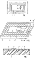
- the circuit unit contains an insulating carrier substrate 1 in the form of a card layer on which the coil 3 lies, the coil ends 15 and 19 of which are conductively connected to the connection points of an integrated circuit 7.
- the integrated circuit can also be cast into a module which, for easier contacting of the integrated circuit 7, has contact surfaces which are conductively connected to the connection points of the integrated circuit 7.
- the coil turns of the coil 3 run along the outer edge of the card layer, so that a large-area coil is created in favor of high energy coupling.
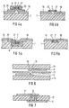
- FIG. 2 shows a circuit unit according to the invention which is not to scale and in a perspective view and which is produced as described below.
- a first coil layer 9 which is shown in broken lines in FIG. 2 and can contain several coil turns, is first applied (the coil layer 9 shown contains, in order to keep the drawing clearer, only a coil turn).
- the coil layer 9 is preferably printed with a conductive lacquer, but it is also possible to spray the coil layer on using a corresponding mask or to etch it out from a conductive coating which is located on the carrier substrate. Other manufacturing techniques are conceivable.
- an insulating layer 11 is applied to the insulating carrier substrate 1, which is shown hatched in FIG. 2 and covers the coil turns of the coil layer 9.
- the isolating Layer 11 has a window 13 and is applied to the coil layer 9 such that the coil end 15 of the coil layer 9 is not covered by it and that at least the coil end of the last coil turn of the coil layer 9 is accessible through the window 13.
- the insulating layer 11 is preferably also printed, but here too it is possible to spray it on using an appropriate mask or to use a thin insulating film as the insulating layer 11, etc.
- a further coil layer 17 is applied to the insulating layer 11, for which purpose the same techniques are used as for the application of the coil layer 9.
- the further coil layer 17 is preferably also printed on.
- the coil layer 17 is conductively connected to the coil layer 9 through the window 13 in the insulating layer 11, so that a coil 3 consisting of the coil layers 9 and 17 is formed.
- the establishment of a conductive connection between the coil layers 9 and 17 can be facilitated in that the coil ends, which are conductively connected to one another, are widened with respect to the coil turns, as is also shown in FIG. 2. Such a broadening is easy to implement in terms of printing technology. Details of the connection technology are described below.
- the coil end 19 of the last applied coil layer is applied in such a way that the production of a conductive connection from the coil ends 15 and 19 to the integrated circuit 7 is particularly simple.
- the coil layers and the insulating layers are applied to the insulating carrier substrate 1 in a kind of frame.
- the coil ends 15 and 19 are guided into the interior of the frame on the insulating carrier substrate 1.
- a superposition of coil turns in a coil layer is avoided in that the inner coil end of the respective coil layer is guided into the part enclosed by the frame, as is also shown in FIG. 2.
- a suitable choice of the coil ends, which are conductively connected to the integrated circuit, can always avoid overlapping of coil turns in a coil position. For example, if the coil end 19 is to be outside the frame, the inner coil end of the coil layer 17 is connected to the coil layer 9 and the outer coil end of the coil layer 17 is guided to the outside.
- an insulating layer with a window to the last coil layer, the free coil end of which is connected to the integrated circuit.
- the free end of the coil can then be guided through the window in any direction over the layer of coils, since there can be no short circuit between the coil turns due to the covering layer.
- the integrated circuit 7 is applied to the uncovered part of the insulating carrier substrate 1, the connection points of which are e.g. can be conductively connected to the coil ends 15 and 19 of the resulting coil by means of bonding wires 21.
- the production of the conductive connections from the integrated circuit 7 to the coil ends 15 and 19 can be simplified by making the coil ends wider than the individual coil turns.
- the printing templates or, in the case of sprayed-on coil layers, the masks used only need to be adapted accordingly. Separate process steps for producing widened coil ends are therefore not necessary.
- FIG. 3 shows a cross section along the line A - A of FIG. 2 in order to clarify the layer sequence.
- the coil layer 9 is applied to the insulating carrier substrate 1 and is covered by the insulating layer 11, which contains a window 13 through which the further coil layer 17 is conductively connected to the coil layer 9.
- Other insulating layers and coil layers can alternate.
- connection between the integrated circuit 7 and the coil ends 15 and 19 is not established via bonding wires, but rather by placing the integrated circuit 7 directly on the coil ends 15 and 19.
- the integrated circuit 7 or a module 23 the contains the integrated circuit 7, either be placed on the already applied coil ends 15 and 19 or the Circuit 7 or module 23 is first inserted into carrier substrate 1 and then overprinted with coil ends 15 and 19.
- Fig. 4 shows cross sections of two embodiments of the circuit unit according to the invention, in which the coil ends 15 and 19 were first printed on the carrier substrate 1 and then the module 23 or the integrated circuit 7 is placed on the coil ends 15 and 19.
- the module 23 or the integrated circuit 7 can optionally be put on immediately after the printing process or only after a short period in which the printed conductive lacquer dries at least partially.
- FIG. 4a shows the carrier substrate 1 with printed coil ends 15 and 19 and the module 23.
- the module 23 contains the integrated circuit 7, which is encased in a sealing compound 8 and the connection points 27 of which are conductively connected to contacts 25 of the module 23 via bonding wires.
- the module 23 is placed on the coil ends 15 and 19 such that the contacts 25 of the module 23 touch the coil ends 15 and 19, respectively.
- the arrangement shown in FIG. 4a can be covered by a cover film, not shown in the figure, which may contain a recess for the module 23.
- the module 23 is placed on the coil ends 15 and 19 so that the sealing compound 8 points away from the coil ends 15 and 19.
- a corresponding recess is to be provided in the carrier substrate 1, which partially accommodates the sealing compound 8. This variant is used in particular when a low overall height of the circuit unit is to be achieved.
- FIG. 4b again shows a carrier substrate 1 with printed coil ends 15 and 19.
- the integrated circuit 7 is placed on the coil ends 15 and 19 such that the connection points 27 of the integrated circuit 7 touch the coil ends 15 and 19, respectively.
- the structure shown in FIG. 4b can also be protected by a cover film, not shown, which can optionally contain a cutout for the integrated circuit 7.
- FIG. 5 shows cross sections of two embodiments of the circuit unit according to the invention, in which the module 23 or the integrated circuit 7 is overprinted for contacting the coil ends 15 and 19.
- the module 23 is fitted into the carrier substrate 1 such that the surface of the module 23 is flush with the surface of the carrier substrate 1.
- the printed after the insertion of the module 23 in the carrier substrate 1 coil ends 15 and 19 extend so far over the surface of the module 23 that they partially cover the contacts 25 of the module 23, so that a conductive connection between the contacts 25 and the coil ends 15 and 19 arises.
- the integrated circuit 7 is inserted into the carrier substrate 1 such that the surface of the integrated circuit 7 is flush with the surface of the carrier substrate 1 and the connection points 27 of the integrated circuit 7 point upwards.
- the coil ends 15 and 19 are printed on the carrier substrate 1 in such a way that they extend beyond the connection points 27 of the integrated circuit 7. In this way, a conductive connection is established between the connection points 27 and the coil ends 15 and 19.
- To embed the integrated circuit 7 in the carrier substrate 1 can either a corresponding recess is provided or the chip can be pressed into the carrier substrate 1 using heat and pressure.
- FIG. 6 shows an embodiment of the circuit unit according to the invention in cross section, in which the through-plating takes place when the individual layers of the circuit unit are laminated together. The layer sequence of the circuit unit before the lamination process is shown.
- a carrier substrate 1a with a coil layer 17 and a carrier substrate 1b with a coil layer 9 are separated from one another by an insulating film 11.
- a window 13 is made in the film 11 by punching out, piercing or by means of a laser beam at a point at which the coil layers 9 and 17 face each other.
- a laminate is produced from the individual layers 1a, 1b and 11 by lamination.
- the lamination process ensures that an electrically conductive connection between the coil layer 9 and the coil layer 17 is created through the window 13. This can be further supported by applying a small portion of conductive adhesive 29 to at least one of the coil layers 9 and 17 opposite the window 13, which flows into the window 13 during lamination and thus creates an electrically conductive connection between the coil layers 9 and 17.
- Fig. 7 shows an embodiment of the circuit unit according to the invention in cross section, in which the insulating film 11 is printed on both sides with coil layers 9 and 17, the coil layers 9 and 17 partially overlap.
- the insulating film 11 has one or more windows 13, which are produced, for example, by punching, piercing or by means of a laser beam. These windows 13 are filled with the printing material, for example a conductive varnish, when the coil layers 9 and 17 are screen printed onto the insulating film 11 and thus establish one or more conductive connections between the coil layers 9 and 17.
- FIG. 8 shows a further exemplary embodiment for the plated-through hole.
- coil layers 9 and 17 are applied on the opposite sides of the insulating film so that they partially overlap.
- at least one thin wire 31 is shot in, which pierces the coil layer 17, the insulating film 11 and at least partially also the coil layer 9 and thus creates a conductive connection between the coil layers 9 and 17.
- the wire 31 can also be passed completely through the coil layer 9 and bent at its end by a suitable device. In order to facilitate the passage of the wire 31, it can be heated in a variant of the exemplary embodiment.
- FIG. 9 shows an exemplary embodiment in which the coil layers 9 and 17 are first applied to the opposite sides of the insulating film 11. Subsequently, in the area in which the opposing coil layers 9 and 17 overlap, at least one window 13 is introduced in the coil layers 9 and 17 and the insulating film 11 in between, for example by punching, piercing or by means of a laser beam. The window 13 is finally filled with a conductive adhesive 33 and thus a conductive connection between the coil layers 9 and 17 is made.
- FIG. 10 shows an exemplary embodiment in which a conductive connection between the coil layers 9 and 17 can be established by means of a connecting element 35.
- the 10a shows the layer sequence of the circuit unit before the lamination process.
- the coil layer 9 is applied to the carrier substrate 1.
- the insulating film 11 is arranged above the carrier substrate 1 and supports the coil layer 17 and has the window 13 in an area opposite the coil layer 9 and adjacent to the coil layer 17.
- the connecting element 35 is arranged on an auxiliary carrier film 37 above the window 13 and overlapping with the coil layer 17.
- the connecting element 35 can consist, for example, of a thermally activatable conductive adhesive.
- FIG. 10b shows the layer structure from FIG. 10a after lamination.
- the in-Fig. 10a layers can be joined together by means of a conventional laminating press under pressure and heat to form a composite.
- the stamp of the laminating press pressing against the top of the structure is shaped in such a way that the connecting element 35 is pressed through the window 13 against the coil layer 9 during the laminating process and connects to it.
- the other end of the connecting element 35 is pressed against the coil layer 17 and connects to it. In this way, a conductive connection between the coil layers 9 and 17 is established.
- the auxiliary carrier film 37 detaches from the connecting element 35 during the lamination process and is subsequently removed.
- the window or windows 13 in the insulating layer 11 can be omitted.
- the coil layers are capacitively coupled.
- the capacitive coupling can also be used for coupling the integrated circuit 7 to the coil 3, so that a conductive connection can also be omitted here.
- Another aspect of the invention consists in lifting previously existing restrictions regarding the high embossability of a circuit unit containing a coil 3. This can be done by various measures, which can be used both with single-layer and with multi-layer coils 3.
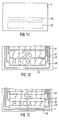
- FIG. 11 shows a top view of a circuit unit, areas 37 and 38 within which embossing is permitted for chip cards in accordance with ISO standard 7811 are each delimited by a dashed line.
- embossing for example, letters and numbers or other characters can be emphasized. If necessary, the embossed characters can be printed on a paper document using a suitable device.
- the embossing can damage the coil 3.
- the lower region 37 is particularly problematic with regard to possible damage to coil turns, since a large-area coil 3 is generally required, and the coil turns therefore run near the edge of the circuit unit.
- FIG. 12 shows an enlarged section of the circuit unit shown in FIG. 11 in a top view.
- a turn 39 between the embossing field 37 and the edge of the carrier substrate 1 arranged. If sufficient space is available, several turns or even all turns of the coil 3 can also run here. Since no embossing takes place in this area, there is also no risk that the turns of the coil 3 will be interrupted by the embossing process. With a multi-layer coil, the space becomes scarce only with higher numbers of turns than with a single-layer coil, since not all turns have to be arranged side by side.
- turns 41 which are so widened in this area that they are wider than the size of the characters embossed there. This ensures that the turns 41 are not interrupted by the embossing process, even if the embossed characters would each cut through a cross section of the turns 41 corresponding to the size of the characters. If there is not enough space for one or more turns 39 outside the high embossing field 37, all the turns 41 can also be guided through the high embossing field 37.
- FIG. 13 also shows an enlarged section of the circuit unit shown in FIG. 11 in a top view.
- the turns of the coil 3 are either guided between the high embossing field 37 and the edge of the circuit unit, turn 39, or following the high embossing lines or between the individual high embossing lines, turns 43.
- the turns 43, the run between the embossing lines or immediately after the embossing lines, are somewhat broadened to compensate for manufacturing tolerances. This ensures that at least a portion of these turns 43 runs on a surface that is not embossed and thus does not involve the risk of interruption of these turns 43 brings itself.
- FIG. 13 shows an enlarged section of the circuit unit shown in FIG. 11 in a top view.
- the properties of the coating material used to produce the windings can be matched as closely as possible to the carrier substrate 1 to which they are applied, so that the coating material does not tear and thus the windings are interrupted when embossed. It is also conceivable to use conductive plastics as coating material which are so elastic that they do not tear when embossed.
- the resistance of the coil 3 may assume inadmissibly high values, since the turns 39 must be very narrow due to the limited space available. This problem can be counteracted by applying the coils 39 in thicker layers, which can be achieved, for example, by multiple printing. Likewise, it is also possible to widen the windings 39 in the areas in which sufficient space is available in order to reduce the resistance.
- the circuit unit can be manufactured both in individual piece production and by means of arches or webs, which are each divided into individual circuit units at the end of production.
- the measures described to improve the circuit unit such as, for example, providing a multilayer coil structure, different through-connection variants being possible, enabling the circuit unit to be embossed by suitable selection of the dimensions and the course, possibly also the material of the coil layers, and direct contacting of the integrated circuit or Modules on the coil can be used individually or in combination.
Abstract
Description
Die Erfindung betrifft eine Schaltungseinheit, die mindestens ein isolierendes Trägersubstrat, auf dem sich eine leitende Spule befindet, und einen integrierten Schaltkreis umfaßt, dessen Anschlußpunkte leitend mit den Spulenenden verbunden sind. Die Erfindung betrifft ferner ein Verfahren zur Herstellung einer solchen Schaltungseinheit.The invention relates to a circuit unit which comprises at least one insulating carrier substrate, on which a conductive coil is located, and an integrated circuit, the connection points of which are conductively connected to the coil ends. The invention further relates to a method for producing such a circuit unit.
Schaltungseinheiten der obengenannten Art sind bereits aus dem Stand der Technik bekannt und werden beispielsweise als kompaktes elektronisches Modul ausgebildet, das in eine Chipkarte für den berührungslosen Datenaustausch mit einem Terminal eingesetzt wird. Aus der US-PS 4,999,742 ist z.B. eine Schaltungseinheit in Form eines elektronischen Moduls mit einem isolierenden Trägersubstrat bekannt, auf das eine ringförmige gewickelte Spule aufgeklebt ist. Die Spulenenden sind in den Aufnahmeraum geführt, der durch die ringförmige Spule entsteht, und dort leitend mit den Anschlußpunkten eines integrierten Schaltkreises verbunden. Der Aufnahmeraum für den integrierten Schaltkreis und die Spulenenden ist zum Schutz dieser empfindlichen Bestandteile vor mechanischen Belastungen mit einer Gußmasse vergossen.Circuit units of the above-mentioned type are already known from the prior art and are designed, for example, as a compact electronic module which is inserted into a chip card for contactless data exchange with a terminal. From U.S. Patent 4,999,742, e.g. a circuit unit in the form of an electronic module with an insulating carrier substrate is known, on which an annular wound coil is glued. The coil ends are guided into the receiving space created by the ring-shaped coil, where they are conductively connected to the connection points of an integrated circuit. The receiving space for the integrated circuit and the coil ends is cast with a casting compound to protect these sensitive components from mechanical loads.
Das aus der US-PS 4,999,742 bekannte elektronische Modul weist einen kompakten Aufbau auf, jedoch muß die Spule in einem separaten Verfahrensschritt gewickelt und in einem weiteren Verfahrensschritt auf das isolierende Trägersubstrat aufgeklebt werden.The electronic module known from US Pat. No. 4,999,742 has a compact structure, but the coil has to be wound in a separate process step and glued to the insulating carrier substrate in a further process step.
Aus der noch nicht veröffentlichten deutschen Patentanmeldung P 44 16 697.4 ist hingegen eine Schaltungseinheit in Form einer Chipkarte bekannt, auf deren einer Kartenschicht des mehrschichtigen Kartenkörpers eine Spule aus einem leitenden Lack aufgedruckt ist, deren Spulenenden leitend mit den Anschlußpunkten eines integrierten Schaltkreises verbunden sind.On the other hand, a circuit unit in the form of a chip card is known from the as yet unpublished German patent application P 44 16 697.4, a coil on one of the card layers of the multi-layer card body is printed from a conductive varnish, the coil ends are conductively connected to the connection points of an integrated circuit.
Der Aufbau der aus der Patentanmeldung 44 16 697.4 bekannten Schaltungseinheit hat den Vorteil, daß die Spule direkt auf eine Kartenschicht aufgedruckt wird und somit der Verfahrensschritt, eine separat gefertigte Spule auf ein isolierendes Trägersubstrat aufzubringen, entfällt. Für einige Anwendungen der Schaltungseinheit ist es jedoch wünschenswert, daß die Spule eine höhere Anzahl von Spulenwindungen aufweist, als sie sich mit dem oben erläuterten Aufbau realisieren läßt. Weiterhin kann es wünschenswert sein, die Schaltungseinheit mit einer Hochprägung zu versehen. Dabei muß jedoch sichergestellt werden, daß die aufgedruckten Spulenwindungen, die in der Regel als eine sehr dünne Schicht ausgebildet sind, nicht unterbrochen werden. Ebenso sollte das Herstellungsverfahren der Schaltungseinheit im Hinblick auf eine preisgünstige Massenfertigung weiter optimiert werden.The structure of the circuit unit known from patent application 44 16 697.4 has the advantage that the coil is printed directly onto a card layer and thus the process step of applying a separately manufactured coil to an insulating carrier substrate is omitted. For some applications of the circuit unit, however, it is desirable that the coil have a higher number of coil turns than can be realized with the construction explained above. Furthermore, it may be desirable to emboss the circuit unit. It must be ensured, however, that the printed coil turns, which are usually designed as a very thin layer, are not interrupted. Likewise, the manufacturing process of the circuit unit should be further optimized with a view to inexpensive mass production.
Es ist deshalb Aufgabe der Erfindung, die obengenannte Schaltungseinheit weiter zu verbessern und dabei insbesondere deren Einsatzmöglichkeiten zu erweitern. Es ist ferner Aufgabe der Erfindung, ein Verfahren zur Herstellung einer solchen Schaltungseinheit vorzuschlagen.It is therefore an object of the invention to further improve the circuit unit mentioned above and in particular to expand its possible uses. It is also an object of the invention to propose a method for producing such a circuit unit.
Die Aufgabe wird durch die nebengeordneten Ansprüche gelöst.The task is solved by the subordinate claims.
Ein Vorteil der Erfindung ist darin zu sehen, daß eine höhere Windungszahl realisiert werden kann als auf dem aus der deutschen Patentanmeldung 44 16 197.4 bekannten Aufbau. Dabei kann die Spule weiterhin direkt auf das Trägersubstrat der Schaltungseinheit aufgebracht werden, so daß ein zusätzlicher Verfahrensschritt für das Aufbringen einer separat gefertigten Spule nicht erforderlich ist. Dies wird dadurch ermöglicht, daß auf dem isolierenden Trägersubstrat im Wechsel Spulenlagen und isolierende Schichten aufgebracht sind, wobei die einzelnen Spulenlagen über Durchkontaktierungen leitend miteinander verbunden sind, so daß eine Spule entsteht. Vorzugsweise werden die Spulenlagen und die isolierenden Schichten aufgedruckt. Alternativ ist es auch möglich, daß die isolierenden Schichten aus dünnen Isolierfolien bestehen, auf denen die Spulenlagen ein- oder beidseitig aufgedruckt sind. Die Durchkontaktierung durch die isolierenden Schichten kann im einfachsten Fall durch das Vorsehen von Fenstern oder Löchern in den isolierenden Schichten erfolgen, durch die hindurch das leitfähige Material der Spulenlagen beim Anfdrucken der Spulenlagen oder beim Zusammenlaminieren der Schichten dringt. Ebenso kann für die Durchkontaktierung auch zusätzliches leitfähiges Material aufgebracht werden oder es können zusätzlich leitfähige Elemente vorgesehen werden.An advantage of the invention is the fact that a higher number of turns can be realized than on the structure known from German patent application 44 16 197.4. The coil can continue to be applied directly to the carrier substrate of the circuit unit, so that an additional process step for the application of a separately manufactured coil is not required. This is made possible by the fact that coil layers and insulating layers are alternately applied to the insulating carrier substrate, the individual coil layers being conductively connected to one another via plated-through holes, so that a coil is formed. The coil layers and the insulating layers are preferably printed on. Alternatively, it is also possible for the insulating layers to consist of thin insulating foils on which the coil layers are printed on one or both sides. In the simplest case, the through-plating through the insulating layers can take place by providing windows or holes in the insulating layers through which the conductive material of the coil layers penetrates when the coil layers are printed on or when the layers are laminated together. Likewise, additional conductive material can also be applied for the plated-through hole or additional conductive elements can be provided.
Ein weiterer Vorteil der Erfindung ist darin zu sehen, daß die Schaltungseinheit besonders einfach im Mehrnutzenverfahren gefertigt werden kann, da bei der Aufbringung der Spulenlagen und je nach Ausführungsform auch der isolierenden Schichten auf die Drucktechnik zurückgegriffen werden kann, bei der die Mehrnutzenfertigung gang und gäbe ist.Another advantage of the invention can be seen in the fact that the circuit unit can be manufactured particularly easily using the multiple-use process, since when applying the coil layers and, depending on the embodiment, also the insulating layers, the printing technology can be used in which multiple-use production is common .
Darüber hinaus hat die Erfindung den Vorteil, daß die Spulenenden auf besonders einfache Art und Weise an die unterschiedlichen Möglichkeiten der Herstellung der leitenden Verbindung zwischen den Spulenenden und den Anschlußpunkten des integrierten Schaltkreises angepaßt werden können.In addition, the invention has the advantage that the coil ends can be adapted in a particularly simple manner to the different possibilities of establishing the conductive connection between the coil ends and the connection points of the integrated circuit.
Weiterhin ist es vorteilhaft, daß die Erfindung eine Hochprägung der Schaltungseinheit uneingeschränkt zulaßt, ohne daß die Gefahr einer Unterbrechung einer oder mehrerer Spulenwindungen besteht. Hierzu werden die Spulenwindungen außerhalb des Hochprägebereiches der Schaltungseinheit geführt oder zwischen den einzelnen Hochprägezeilen, wobei die Breite der Spulenwindungen zum Ausgleich von Fertigungstoleranzen jeweils größer sein kann als der Zeilenabstand oder die Spulenwindungen verlaufen im Bereich der hochgeprägten Zeichen, sind jedoch breiter als die Zeichengröße.Furthermore, it is advantageous that the invention permits the embossing of the circuit unit without restriction, without the risk of interruption of one or more coil turns. For this, the Coil turns are outside the embossed area of the circuit unit or between the individual embossed lines, whereby the width of the coil turns to compensate for manufacturing tolerances can be greater than the line spacing or the coil turns are in the area of the embossed characters, but are wider than the character size.
Ausführungsbeispiele und weitere Vorteile der Erfindung sind in Zusammenhang mit den nachstehenden Figuren erläutert, darin zeigen:
- Fig. 1
- eine Schaltungeinheit in Aufsicht,
- Fig. 2
- eine Schaltungseinheit in perspektivischer Sicht,
- Fig. 3
- einen Querschnitt entlang der Linie A - A der Fig. 2,
- Fig. 4, 5
- Ausführungsbeispiele für die Kontaktierung einer Spule an einen integrierten Schaltkreis bzw. an ein Modul,
- Fig. 6 bis 10
- Ausführungsbeispiele für die Durchkontaktierung zur Herstellung einer leitenden Verbindung zwischen gegenüberliegenden Spulenlagen im Querschnitt,
- Fig. 11
- eine Schaltungseinheit mit eingezeichneten Hochprägefeldern in Aufsicht,
- Fig. 12, 13
- Ausführungsbeispiele für die Ausbildung und Anordnung von Spulenwindungen als vergrößerten Ausschnitt in Aufsicht.
- Fig. 1
- a circuit unit under supervision,
- Fig. 2
- a circuit unit in perspective view,
- Fig. 3
- 3 shows a cross section along the line AA of FIG. 2,
- 4, 5
- Exemplary embodiments for contacting a coil to an integrated circuit or to a module,
- 6 to 10
- Exemplary embodiments for the through-connection for producing a conductive connection between opposite coil layers in cross section,
- Fig. 11
- a circuit unit with high embossing fields shown in supervision,
- Fig. 12, 13
- Embodiments for the formation and arrangement of coil turns as an enlarged detail in supervision.
Fig. 1 zeigt systematisch eine Schaltungseinheit in Form einer Chipkarte für den berührungslosen Datenaustausch in Aufsicht. Die Abmessungen solcher Chipkarten sind mit den Abmessungen der Chipkarten für den berührenden Datenaustausch identisch, die in der ISO-Norm 7810 festgelegt sind. Die Schaltungseinheit enthält ein isolierendes Trägersubstrat 1 in Form einer Kartenschicht, auf dem die Spule 3 liegt, deren Spulenenden 15 und 19 leitend mit den Anschlußpunkten eines integrierten Schaltkreises 7 verbunden sind. Der integrierte Schaltkreis kann auch zu einem Modul vergossen sein, das zur leichteren Kontaktierung des integrierten Schaltkreises 7 Kontaktflächen aufweist, die leitend mit den Anschlußpunkten des integrierten Schaltkreises 7 verbunden sind. Die Spulenwindungen der Spule 3 laufen am äußeren Rand der Kartenschicht entlang, damit zugunsten einer hohen Energieeinkopplung eine großflächige Spule entsteht.1 systematically shows a circuit unit in the form of a chip card for contactless data exchange under supervision. The dimensions of such chip cards are identical to the dimensions of the chip cards for contacting data exchange, which are specified in ISO standard 7810. The circuit unit contains an
Fig. 2 zeigt nicht maßstabsgetreu und in perspektivischer Sicht eine erfindungsgemäße Schaltungseinheit, die wie folgt beschrieben hergestellt wird. Auf das isolierende Trägersubstrat 1, das z.B. in Form einer Kartenschicht vorliegt (siehe Fig. 1), wird zunächst eine erste Spulenlage 9, die in der Fig. 2 strichliniert gezeigt ist und mehrere Spulenwindungen enthalten kann, aufgebracht (die gezeigte Spulenlage 9 enthält, um die Zeichnung übersichtlicher zu halten, nur eine Spulenwindung). Vorzugsweise wird die Spulenlage 9 mit einem leitenden Lack aufgedruckt, es ist aber auch möglich, die Spulerlage unter Verwendung einer entsprechenen Maske aufzusprühen, bzw. aus einer leitenden Beschichtung, die sich auf dem Trägersubstrat befindet, auszuätzen. Andere Herstellungstechniken sind denkbar.FIG. 2 shows a circuit unit according to the invention which is not to scale and in a perspective view and which is produced as described below. On the
Nach dem Aufbringen der Spulenlage 9 wird auf das isolierende Trägersubstrat 1 eine isolierende Schicht 11 aufgebracht, die in der Fig. 2 schraffiert gezeigt ist und die Spulenwindungen der Spulenlage 9 abdeckt. Die isolierende Schicht 11 weist ein Fenster 13 auf und wird auf die Spulenlage 9 derart aufgebracht, daß das Spulenende 15 der Spulenlage 9 nicht von ihr abgedeckt wird und daß zumindest das Spulenende der letzten Spulenwindung der Spulenlage 9 durch das Fenster 13 zugänglich ist. Vorzugsweise wird die isolierende Schicht 11 ebenfalls aufgedruckt, auch hier ist es aber möglich, sie unter Verwendung einer entsprechenden Maske aufzusprühen oder als isolierende Schicht 11 eine dünne Isolierfolie zu verwenden, etc.After the application of the
In einem weiteren Verfahrensschritt wird auf die isolierende Schicht 11 eine weitere Spulenlage 17 aufgebracht, wozu die gleichen Techniken wie beim Aufbringen der Spulenlage 9 verwendet werden. Vorzugsweise wird auch die weitere Spulenlage 17 aufgedruckt. Die Spulenlage 17 wird durch das Fenster 13 in der isolierenden Schicht 11 leitend mit der Spulenlage 9 verbunden, so daß eine Spule 3, bestehend aus den Spulenlagen 9 und 17, entsteht. Die Herstellung einer leitenden Verbindung zwischen den Spulenlagen 9 und 17 kann dadurch erleichtert werden, daß man die Spulenenden, die leitend miteinander verbunden werden, gegenüber den Spulenwindungen verbreitert ausbildet, so wie es auch in der Fig. 2 gezeigt ist. Eine solche Verbreiterung ist drucktechnisch einfach realisierbar. Einzelheiten zur Verbindungstechnik werden weiter unten beschrieben.In a further method step, a
Das Aufbringen weiterer isolierender Schichten und Spulenlagen in der erläuterten Art und Weise kann gegebenenfalls ein- oder mehrfach wiederholt werden, bis die aus den Spulenlagen zusammengesetzte Spule 3 der Schaltungseinheit die gewünschte Anzahl von Windungen aufweist. Hierbei ist darauf zu achten, daß das Spulenende 15 der zuerst aufgedruckten Spulenlage nicht abgedeckt wird und daß die Schaltungseinheit eine vorgegebene Höhe nicht überschreitet. Bei dem Aufdrucken der letzten Spulenlage kann das Spulenende 15 der zuerst aufgedruckten Spulenlage nochmals mit einem leitenden Lack überdruckt werden. Man erhält dann zwei frisch aufgedruckte Spulenenden 15 und 19, die sich besonders einfach leitend mit dem integrierten Schaltkreis verbinden lassen.The application of further insulating layers and coil layers in the manner described can, if necessary, be repeated one or more times until the
Das Spulenende 19 der zuletzt aufgebrachten Spulenlage, in der Fig. 2 also der Spulenlage 17, wird so aufgebracht, daß die Herstellung einer leitenden Verbindung von den Spulenenden 15 und 19 zu dem integrierten Schaltkreis 7 besonders einfach möglich ist. Bei dem in der Fig. 2 gezeigten Ausführungsbeispiel der Erfindung werden die Spulenlagen und die isolierenden Schichten auf das isolierende Trägersubstrat 1 in einer Art Rahmen aufgebracht. Die Spulenenden 15 und 19 werden in dem gezeigten Ausführungsbeispiel in das Rahmeninnere auf das isolierende Trägersubstrat 1 geführt. Hierbei wird eine Überlagerung von Spulenwindungen in einer Spulenlage dadurch vermieden, daß das innenliegende Spulenende der jeweiligen Spulenlage in den von dem Rahmen umschlossenen Teil geführt wird, wie es auch in der Fig. 2 gezeigt ist.The
Durch eine geeignete Wahl der Spulenenden, die leitend mit dem integrierten Schaltkreis verbunden werden, kann eine Überlagerung von Spulenwindungen in einer Spulenlage immer vermieden werden. Soll beispielsweise das Spulenende 19 außerhalb des Rahmens liegen, so wird das innenliegende Spulenende der Spulenlage 17 mit der Spulenlage 9 verbunden und das außenliegende Spulenende der Spulenlage 17 nach außen geführt.A suitable choice of the coil ends, which are conductively connected to the integrated circuit, can always avoid overlapping of coil turns in a coil position. For example, if the
Alternativ ist es auch möglich, auf die letzte Spulenlage, deren freies Spulenende mit dem integrierten Schaltkreis verbunden wird, eine isolierende Schicht mit Fenster aufzubringen. Durch das Fenster kann dann das freie Spulenende über die Spulenlage in eine beliebige Richtung geführt werden, da es wegen der abdeckenden Schicht zu keinem Kurzschluß zwischen den Spulenwindungen kommen kann.Alternatively, it is also possible to apply an insulating layer with a window to the last coil layer, the free coil end of which is connected to the integrated circuit. The free end of the coil can then be guided through the window in any direction over the layer of coils, since there can be no short circuit between the coil turns due to the covering layer.
Gemaß dem Ausführungsbeispiel der Fig. 2 wird auf den nicht abgedeckten Teil des isolierenden Trägersubstrats 1 der integrierte Schaltkreis 7 aufgebracht, dessen Anschlußpunkte z.B. mittels Bonddrähtchen 21 leitend mit den Spulenenden 15 und 19 der entstandenen Spule verbunden werden. Hierbei kann die Herstellung der leitenden Verbindungen von dem integrierten Schaltkreis 7 zu den Spulenenden 15 und 19 dadurch vereinfacht werden, daß man die Spulenenden breiter als die einzelnen Spulenwindungen ausbildet. Dazu brauchen die Druckvorlagen bzw. bei aufgesprühten Spulenlagen die verwendeten Masken lediglich entsprechend angepaßt zu werden. Gesonderte Verfahrensschritte zur Erzeugung verbreiterter Spulenenden sind also nicht notwendig.According to the embodiment of FIG. 2, the
Fig. 3 zeigt zur Verdeutlichung der Schichtfolge einen Querschnitt entlang der Linie A - A der Fig. 2. Auf das isolierende Trägersubstrat 1 ist die Spulenlage 9 aufgebracht, die durch die isolierende Schicht 11 abgedeckt ist, die ein Fenster 13 enthält, durch das die weitere Spulenlage 17 leitend mit der Spulenlage 9 verbunden wird. Weitere isolierende Schichten und Spulenlagen können sich im Wechsel anschließen.FIG. 3 shows a cross section along the line A - A of FIG. 2 in order to clarify the layer sequence. The
In einer Variante wird die Verbindung zwischen dem integrierten Schaltkreis 7 und den Spulenenden 15 und 19 nicht über Bonddrähtchen hergestellt, sondern durch direktes Aufsetzen des integrierten Schaltkreises 7 auf die Spulenenden 15 und 19. Hierzu kann der integrierte Schaltkreis 7 bzw. ein Modul 23, das den integrierten Schaltkreis 7 enthält, entweder auf die bereits aufgebrachten Spulenenden 15 und 19 aufgesetzt werden oder der Schaltkreis 7 bzw. das Modul 23 wird zuerst in das Trägersubstrat 1 eingesetzt und anschließend mit den Spulenenden 15 und 19 überdruckt.In a variant, the connection between the
Fig. 4 zeigt Querschnitte zweier Ausführungsformen der erfindungsgemäßen Schaltungseinheit, bei denen zuerst die Spulenenden 15 und 19 auf das Trägersubstrat 1 aufgedruckt wurden und anschließend das Modul 23 bzw. der integrierte Schaltkreis 7 auf die Spulenenden 15 und 19 aufgesetzt wird. Das Aufsetzen des Moduls 23 bzw. des integrierten Schaltkreises 7 kann wahlweise unmittelbar nach dem Druckvorgang erfolgen oder erst nach einer kurzen Zeitspanne, in der der aufgedruckte Leitlack zumindest teilweise trocknet.Fig. 4 shows cross sections of two embodiments of the circuit unit according to the invention, in which the coil ends 15 and 19 were first printed on the
Fig. 4a zeigt das Trägersubstrat 1 mit aufgedruckten Spulenenden 15 und 19 und dem Modul 23. Das Modul 23 enthält den integrierten Schaltkreis 7, der von einer Vergußmasse 8 umhüllt ist und dessen Anschlußpunkte 27 mit Kontakten 25 des Moduls 23 über Bonddrähtchen leitend verbunden sind. Auf die Spulenenden 15 und 19 ist das Modul 23 so aufgesetzt, daß die Kontakte 25 des Moduls 23 die Spulenenden 15 bzw. 19 berühren. Die in Fig. 4a dargestellte Anordnung kann durch eine nicht figürlich dargestellte Deckfolie, die gegebenenfalls eine Aussparung für das Modul 23 enthält, abgedeckt werden. Bei dem in Fig. 4a dargestellten Ausführungsbeispiel ist das Modul 23 so auf die Spulenenden 15 und 19 aufgesetzt, daß die Vergußmasse 8 von den Spulenenden 15 und 19 wegweist. Es ist jedoch auch möglich, das Modul um 180° gedreht aufzusetzen. In diesem Fall ist im Trägersubstrat 1 eine entsprechende Aussparung vorzusehen, die die Vergußmasse 8 teilweise aufnimmt. Diese Variante wird insbesondere dann eingesetzt, wenn eine niedrige Bauhöhe der Schaltungseinheit erzielt werden soll.4a shows the
Fig. 4b zeigt wiederum ein Trägersubstrat 1 mit aufgedruckten Spulenenden 15 und 19. Auf die Spulenenden 15 und 19 ist der integrierte Schaltkreis 7 so aufgesetzt, daß die Anschlußpunkte 27 des integrierten Schaltkreises 7 die Spulenenden 15 bzw. 19 berühren. Wie beim Ausführungsbeispiel nach Fig. 4a kann auch der in Fig. 4b dargestellte Aufbau durch eine nicht dargestellte Abdeckfolie geschützt werden, die gegebenenfalls eine Aussparung für den integrierten Schaltkreis 7 enthalten kann.4b again shows a
Fig. 5 zeigt Querschnitte zweier Ausführungsformen der erfindungsgemäßen Schaltungseinheit, bei denen das Modul 23 bzw. der integrierte Schaltkreis 7 zur Kontaktierung mit den Spulenenden 15 und 19 überdruckt wird.5 shows cross sections of two embodiments of the circuit unit according to the invention, in which the
In Fig. 5a ist das Modul 23 so in das Trägersubstrat 1 eingepaßt, daß die Oberfläche des Moduls 23 bündig mit der Oberfläche des Trägersubstrats 1 abschließt. Die nach dem Einsetzen des Moduls 23 in das Trägersubstrat 1 aufgedruckten Spulenenden 15 und 19 erstrecken sich so weit über die Oberfläche des Moduls 23, daß sie die Kontakte 25 des Moduls 23 teilweise überdecken, so daß eine leitende Verbindung zwischen den Kontakten 25 und den Spulenenden 15 und 19 entsteht.5a, the
In Fig. 5b ist anstelle des Moduls 23 der integrierte Schaltkreis 7 so in das Trägersubstrat 1 eingesetzt, daß die Oberfläche des integrierten Schaltkreises 7 mit der Oberfläche des Trägersubstrats 1 bündig abschließt und die Anschlußpunkte 27 des integrierten Schaltkreises 7 nach oben weisen. Auf das Trägersubstrat 1 sind die Spulenenden 15 und 19 derart aufgedruckt, daß sie sich bis über die Anschlußpunkte 27 des integrierten Schaltkreises 7 erstrecken. Auf diese Weise wird jeweils eine leitende Verbindung zwischen den Anschlußpunkten 27 und den Spulenenden 15 und 19 hergestellt. Zur Einbettung des integrierten Schaltkreises 7 in das Trägersubstrat 1 kann entweder eine entsprechende Aussparung vorgesehen werden oder der Chip kann unter Anwendung von Hitze und Druck in das Trägersubstrat 1 eingepreßt werden.In Fig. 5b, instead of the
Im folgenden werden einige Varianten für die Durchkontaktierung beschrieben, mit deren Hilfe elektrisch leitende Verbindungen zwischen zwei Spulenlagen bzw. zwischen einer Spulenlage und einem Anschlußpunkt 27 des integrierten Schaltkreises 7 oder einem Kontakt 25 des Moduls 23 durch die isolierende Schicht 11 hindurch, beispielsweise eine dünne Isolierfolie, hergestellt werden können.In the following, some variants for the plated-through hole are described, with the aid of which electrically conductive connections between two coil layers or between a coil layer and a
Fig. 6 zeigt eine Ausführungsform der erfindungsgemäßen Schaltungseinheit im Querschnitt, bei der die Durchkontaktierung heim Zusammenlaminieren der einzelnen Schichten der Schaltungseinheit erfolgt. Dargestellt ist die Schichtenfolge der Schaltungseinheit vor dem Laminiervorgang.FIG. 6 shows an embodiment of the circuit unit according to the invention in cross section, in which the through-plating takes place when the individual layers of the circuit unit are laminated together. The layer sequence of the circuit unit before the lamination process is shown.
Gemäß Fig. 6 werden ein Trägersubstrat 1a mit einer Spulenlage 17 und ein Trägersubstrat 1b mit einer Spulenlage 9 durch eine Isolierfolie 11 voneinander getrennt. In die Folie 11 ist durch Ausstanzen, Durchstechen oder mittels eines Laserstrahls ein Fenster 13 an einer Stelle eingebracht, an der sich die Spulenlagen 9 und 17 gegenüberstehen. Durch Laminieren wird aus den einzelnen Schichten 1a, 1b und 11 ein Verbund hergestellt. Gleichzeitig wird durch den Laminiervorgang erreicht, daß durch das Fenster 13 hindurch eine elektrisch leitende Verbindung zwischen der Spulenlage 9 und der Spulenlage 17 entsteht. Dies kann noch dadurch unterstützt werden, daß auf wenigstens einer der Spulenlagen 9 und 17 gegenüber dem Fenster 13 eine kleine Portion Leitkleber 29 aufgebracht wird, der beim Laminieren in das Fenster 13 fließt und so eine elektrisch leitende Verbindung zwischen den Spulenlagen 9 und 17 herstellt.6, a
Fig. 7 zeigt ein Ausführungsbeispiel der erfindungsgemäßen Schaltungseinheit im Querschnitt, bei dem die Isolierfolie 11 beidseitig mit Spulenlagen 9 bzw. 17 bedruckt ist, wobei die Spulenlagen 9 und 17 teilweise überlappen. In dem Überlappungsbereich weist die Isolierfolie 11 ein oder mehrere Fenster 13 auf, die beispielsweise durch Stanzen, Durchstechen oder mittels eines Laserstrahls erzeugt sind. Diese Fenster 13 werden beim Aufdrucken der Spulenlagen 9 und 17 im Siebdruckverfahren auf die Isolierfolie 11 mit dem Druckmaterial, beispielsweise einem leitendem Lack, gefüllt und stellen so eine bzw. mehrere leitende Verbindungen zwischen den Spulenlagen 9 und 17 her.Fig. 7 shows an embodiment of the circuit unit according to the invention in cross section, in which the insulating
Fig. 8 zeigt ein weiteres Ausführungsbeispiel für die Durchkontaktierung. Wie in Fig. 8 sind auf den gegenüberliegenden Seiten der Isolierfolie 11 Spulenlagen 9 und 17 so aufgebracht, daß sie sich teilweise überlappen. In dem Überlappungsbereich wird wenigstens ein dünner Draht 31 eingeschossen, der die Spulenlage 17, die Isolierfolie 11 und wenigstens teilweise auch die Spulenlage 9 durchstößt und so eine leitende Verbindung zwischen den Spulenlagen 9 und 17 herstellt. Der Draht 31 kann auch ganz durch die Spulenlage 9 durchgeführt werden und durch eine geeignete Vorrichtung an seinem Ende umgebogen werden. Um das Durchführen des Drahtes 31 zu erleichtern, kann dieser in einer Variante des Ausführungsbeispiels erhitzt werden.8 shows a further exemplary embodiment for the plated-through hole. As in Fig. 8 11
Fig. 9 zeigt ein Ausführungsbeispiel, bei dem zunächst auf den gegenüberliegenden Seiten der Isolierfolie 11 die Spulenlagen 9 und 17 aufgebracht werden. Anschließend wird in dem Bereich, in dem sich die gegenüberliegenden Spulenlagen 9 und 17 überlappen, wenigstens ein Fenster 13 in den Spulenlagen 9 und 17 und die dazwischenliegende Isolierfolie 11 eingebracht, beispielsweise durch Stanzen, Durchstechen oder mittels eines Laserstrahls. Das Fenster 13 wird schließlich mit einem Leitkleber 33 aufgefüllt und so eine leitende Verbindung zwischen den Spulenlagen 9 und 17 hergestellt.FIG. 9 shows an exemplary embodiment in which the coil layers 9 and 17 are first applied to the opposite sides of the insulating
In Fig. 10 ist ein Ausführungsbeispiel dargestellt, bei dem mittels eines Verbindungselements 35 eine leitende Verbindung zwischen den Spulenlagen 9 und 17 hergestellt werden kann.10 shows an exemplary embodiment in which a conductive connection between the coil layers 9 and 17 can be established by means of a connecting
Fig. 10a zeigt die Schichtfolge der Schaltungseinheit vor dem Laminierprozeß. Auf dem Trägersubstrat 1 ist die Spulenlage 9 aufgebracht. Oberhalb des Trägersubstrats 1 ist die Isolierfolie 11 angeordnet, die die Spulenlage 17 trägt und in einem Bereich gegenüber der Spulenlage 9 und angrenzend an die Spulenlage 17 das Fenster 13 aufweist. Über dem Fenster 13 und überlappend mit der Spulenlage 17 ist das Verbindungselement 35 auf einer Hilfsträgerfolie 37 angeordnet. Das Verbindungselement 35 kann beispielsweise aus einem thermisch aktivierbaren Leitkleber bestehen.10a shows the layer sequence of the circuit unit before the lamination process. The
Fig. 10b zeigt den Schichtaufbau aus Fig. 10a nach dem Laminieren. Die in-Fig. 10a dargestellten Schichten können mittels einer herkömmlichen Laminierpresse unter Druck und Hitze zu einem Verbund zusammengefügt werden. Der gegen die Oberseite des Aufbaus drückende Stempel der Laminierpresse ist dabei so geformt, daß das Verbindungselement 35 beim Laminiervorgang durch das Fenster 13 gegen die Spulenlage 9 gepreßt wird und sich mit dieser verbindet. Das andere Ende des Verbindungselements 35 wird gegen die Spulenlage 17 gepreßt und verbindet sich dabei mit dieser. Auf diese Art und Weise wird eine leitende Verbindung zwischen den Spulenlagen 9 und 17 hergestellt. Die Hilfsträgerfolie 37 löst sich während des Laminiervorgangs von dem Verbindungselement 35 und wird anschließend entfernt.FIG. 10b shows the layer structure from FIG. 10a after lamination. The in-Fig. 10a layers can be joined together by means of a conventional laminating press under pressure and heat to form a composite. The stamp of the laminating press pressing against the top of the structure is shaped in such a way that the connecting
In einer Variante der Erfindung können das oder die Fenster 13 in der isolierenden Schicht 11 entfallen. Bei dieser Variante besteht zwischen den einzelnen Spulenlagen keine leitende Verbindung. Die Spulenlagen sind stattdessen kapazitiv gekoppelt. Die kapazitive Kopplung kann auch für die Kopplung des integrierten Schaltkreises 7 an die Spule 3 verwendet werden, so daß hier ebenfalls eine leitende Verbindung entfallen kann.In a variant of the invention, the window or
Ein weiterer Aspekt der Erfindung besteht darin, bisher bestehende Einschränkungen bezüglich der Hochprägbarkeit einer Schaltungseinheit, die eine Spule 3 enthält, aufzuheben. Dies kann durch verschiedene Maßnahmen geschehen, die jeweils sowohl bei einschichtigen als auch bei mehrschichtigen Spulen 3 anwendbar sind.Another aspect of the invention consists in lifting previously existing restrictions regarding the high embossability of a circuit unit containing a
In Fig. 11 ist eine Schaltungseinheit in Aufsicht dargestellt, wobei Bereiche 37 und 38, innerhalb derer gemäß der ISO-Norm 7811 bei Chipkarten Hochprägungen zulässig sind, jeweils durch eine gestrichelte Linie abgegrenzt sind. Mit der Hochprägung können beispielsweise Buchstaben und Zahlen oder andere Zeichen hervorgehoben werden. Die hochgeprägten Zeichen können bei Bedarf mit einer geeigneten Vorrichtung auf einen Papierbeleg abgedruckt werden. Durch das Hochprägen kann es jedoch zu einer Beschädigung der Spule 3 kommen. Besonders problematisch im Hinblick auf eine mögliche Beschädigung von Spulenwindungen ist der untere Bereich 37, da in der Regel eine großflächige Spule 3 benötigt wird, und die Spulenwindungen daher in der Nähe des Randes der Schaltungseinheit verlaufen.11 shows a top view of a circuit unit,
Fig. 12 zeigt einen vergrößerten Ausschnitt der in Fig. 11 dargestellten Schaltungseinheit in Aufsicht. Um eine Unterbrechung der Windungen der Spule 3 zu verhindern, ist in dem Ausführungsbeispiel gemäß Fig. 3 eine Windung 39 zwischen dem Hochprägefeld 37 und dem Rand des Trägersubstrats 1 angeordnet. Falls ausreichend Platz zur Verfügung steht, können hier auch mehrere Windungen oder sogar sämtliche Windungen der Spule 3 verlaufen. Da in diesem Bereich keine Prägung stattfindet, besteht auch nicht die Gefahr, daß die Windungen der Spule 3 durch den Prägevorgang unterbrochen werden. Bei einer mehrschichtigen Spule wird der Platz erst bei höheren Windungszahlen knapp als bei einer einschichtigen Spule, da nicht alle Windungen nebeneinander angeordnet werden müssen.FIG. 12 shows an enlarged section of the circuit unit shown in FIG. 11 in a top view. In order to prevent an interruption of the turns of the
Im Bereich des Hochprägefelds 37 verlaufen Windungen 41, die in diesem Bereich so stark verbreitert sind, daß sie breiter sind als die Größe der dort eingeprägten Zeichen. Dadurch ist sichergestellt, daß die Windungen 41 durch den Prägevorgang nicht unterbrochen werden, selbst wenn die eingeprägten Zeichen jeweils einen der Zeichengröße entsprechenden Querschnitt der Windungen 41 durchtrennen würden. Falls nicht ausreichend Platz für eine oder mehrere Windungen 39 außerhalb des Hochprägefelds 37 ist, können auch sämtliche Windungen 41 durch das Hochprägefeld 37 geführt werden.In the area of the
Fig. 13 zeigt ebenfalls einen vergrößerten Ausschnitt der in Fig. 11 dargestellten Schaltungseinheit in Aufsicht. Gemäß dem in Fig. 13 dargestellten Ausführungsbeispiel sind die Windungen der Spule 3 entweder zwischen dem Hochprägefeld 37 und dem Rand der Schaltungseinheit geführt, Windung 39, bzw. im Anschluß an die Hochprägezeilen oder zwischen den einzelnen Hochprägezeilen, Windungen 43. Die Windungen 43, die zwischen den Hochprägezeilen verlaufen bzw. unmittelbar im Anschluß an die Hochprägezeilen, sind dabei etwas verbreitert, um Fertigungstoleranzen auszugleichen. Dadurch ist sichergestellt, daß zumindest ein Teilbereich dieser Windungen 43 auf einer Fläche verläuft, die nicht hochgeprägt wird und somit auch nicht die Gefahr einer Unterbrechung dieser Windungen 43 mit sich bringt. Auch bei dem in Fig. 13 dargestellten Ausführungsbeispiel hängt es von der genauen Abmessung der Windungen ab, ob gar keine oder wenigstens eine Windung 39 am Hochprägefeld vorbeigeführt werden kann, d.h. ob zwischen dem Hochprägefeld 37 und dem Rand des Trägersubstrats ausreichend Platz für eine oder gar für mehrere Windungen 39 ist. Ebenso können die in Fig. 12 und 13 dargestellten Windungsvarianten auch kombiniert werden.FIG. 13 also shows an enlarged section of the circuit unit shown in FIG. 11 in a top view. According to the exemplary embodiment shown in FIG. 13, the turns of the
Neben den bereits geschilderten Maßnahmen sind noch weitere denkbar, um eine Unterbrechung der Windungen der Spule 3 durch das Hochprägen zu verhindern. Beispielsweise können die Eigenschaften des zur Herstellung der Windungen verwendeten Beschichtungsmaterials möglichst stark dem Trägersubstrat 1, auf das sie aufgebracht werden, angeglichen werden, damit es beim Hochprägen nicht zu einem Reißen des Beschichtungsmaterials und somit zu einer Unterbrechung der Windungen kommt. Ebenso ist es denkbar, als Beschichtungsmaterial leitfähige Kunststoffe einzusetzen, die so elastisch sind, daß sie beim Hochprägen nicht reißen.In addition to the measures already described, other measures are also conceivable in order to prevent the turns of the
Bei den Ausführungsformen, bei denen eine oder mehrere Windungen 39 zwischen dem Hochprägefeld 37 und dem Rand der Schaltungseinheit geführt werden, kann der Widerstand der Spule 3 unter Umständen unzulässig hohe Werte annehmen, da wegen des geringen Platzangebots die Windungen 39 sehr schmal sein müssen. Diesem Problem kann dadurch gegengesteuert werden, daß man die Windungen 39 in größeren Schichtstärken aufbringt, was beispielsweise durch einen Mehrfachdruck erreicht werden kann. Ebenso ist es auch möglich, zur Reduzierung des Widerstands die Windungen 39 in den Bereichen, in denen ausreichend Platz zur Verfügung steht, zu verbreitern.In the embodiments in which one or more turns 39 are routed between the
Die Herstellung der Schaltungseinheit kann sowohl in Einzelstückfertigung als auch über Bogen oder Bahnen erfolgen, die jeweils am Ende der Fertigung in einzelne Schaltungseinheiten zerteilt werden.The circuit unit can be manufactured both in individual piece production and by means of arches or webs, which are each divided into individual circuit units at the end of production.
Die beschriebenen Maßnahmen zur Verbesserung der Schaltungseinheit, wie beispielsweise Bereitstellen eines mehrschichtigen Spulenaufbaus, wobei verschiedene Durchkontaktierungsvarianten möglich sind, Ermöglichen der Hochprägung der Schaltungseinheit durch geeignete Wahl der Abmessungen und des Verlaufs, gegebenenfalls auch des Materials der Spulenlagen und direkte Kontaktierung des integrierten Schaltkreises bzw. des Moduls an die Spule, können jeweils sowohl einzeln als auch in Kombination eingesetzt werden.The measures described to improve the circuit unit, such as, for example, providing a multilayer coil structure, different through-connection variants being possible, enabling the circuit unit to be embossed by suitable selection of the dimensions and the course, possibly also the material of the coil layers, and direct contacting of the integrated circuit or Modules on the coil can be used individually or in combination.
Claims (23)
Applications Claiming Priority (2)
| Application Number | Priority Date | Filing Date | Title |
|---|---|---|---|
| DE19527359 | 1995-07-26 | ||
| DE19527359A DE19527359A1 (en) | 1995-07-26 | 1995-07-26 | Circuit unit and method for manufacturing a circuit unit |
Publications (3)
| Publication Number | Publication Date |
|---|---|
| EP0756244A2 true EP0756244A2 (en) | 1997-01-29 |
| EP0756244A3 EP0756244A3 (en) | 1998-12-09 |
| EP0756244B1 EP0756244B1 (en) | 2003-03-12 |
Family
ID=7767864
Family Applications (1)
| Application Number | Title | Priority Date | Filing Date |
|---|---|---|---|
| EP96112037A Expired - Lifetime EP0756244B1 (en) | 1995-07-26 | 1996-07-25 | Electronic unit and method of producing that unit |
Country Status (4)
| Country | Link |
|---|---|
| US (2) | US6049461A (en) |
| EP (1) | EP0756244B1 (en) |
| DE (2) | DE19527359A1 (en) |
| ES (1) | ES2191073T3 (en) |
Cited By (18)
| Publication number | Priority date | Publication date | Assignee | Title |
|---|---|---|---|---|
| DE19642378A1 (en) * | 1996-10-14 | 1998-04-16 | Fraunhofer Ges Forschung | Contactless chip card |
| DE19733348A1 (en) * | 1997-08-01 | 1998-09-03 | Siemens Ag | Data carrier card with coil for contactless data transmission |
| WO1998048378A2 (en) * | 1997-04-21 | 1998-10-29 | Siemens Aktiengesellschaft | Card inlay for chip cards |
| WO1999003165A1 (en) * | 1997-07-07 | 1999-01-21 | Siemens Aktiengesellschaft | Chip card and process for contacting an antenna embedded in a chip card |
| FR2769390A1 (en) * | 1997-10-08 | 1999-04-09 | Gemplus Card Int | Fabrication of smart cards for both contact and non-contact operation |
| WO2000021030A1 (en) * | 1998-10-06 | 2000-04-13 | Intermec Ip Corp. | Rfid transponder having improved rf characteristics |
| DE19840220A1 (en) * | 1998-09-03 | 2000-04-20 | Fraunhofer Ges Forschung | Transponder module and method for producing the same |
| DE19847088A1 (en) * | 1998-10-13 | 2000-05-18 | Ksw Microtec Ges Fuer Angewand | Flat carrier for semiconductor chips and method for its production |
| WO2000043952A1 (en) * | 1999-01-22 | 2000-07-27 | Intermec Ip Corp. | Rfid transponder |
| DE19940480A1 (en) * | 1999-08-26 | 2001-03-08 | Orga Kartensysteme Gmbh | Conductor carrier layer for lamination into a chip card, chip card with a conductor carrier carrier layer and method for producing a chip card |
| EP1107175A2 (en) * | 1999-12-10 | 2001-06-13 | Sony Corporation | Embossed IC card and information reading system therefor |
| JP2002259920A (en) * | 2001-02-27 | 2002-09-13 | Sony Corp | Ic card capable of being embossed, its manufacturing method, embossed ic card and transaction processing system thereby |
| EP1840802A1 (en) * | 2006-03-30 | 2007-10-03 | Fujitsu Limited | RFID tag and manufacturing method thereof |
| DE102009050199A1 (en) | 2009-10-21 | 2011-04-28 | Giesecke & Devrient Gmbh | Production of conductor structures on plastic films using nanoinks |
| DE102010015659A1 (en) | 2010-04-20 | 2011-10-20 | Giesecke & Devrient Gmbh | Transfer method for the production of conductor structures by means of nanoinks |
| DE102011016512A1 (en) * | 2011-04-08 | 2012-10-11 | Giesecke & Devrient Gmbh | Method for fitting substrate e.g. plastic-film, with electrically-conducting structures i.e. coils, in integrated circuit of chip card, involves connecting electrically-conducting structures by electrically-conducting connection |
| DE102015014408A1 (en) * | 2015-11-06 | 2017-05-11 | Giesecke & Devrient Gmbh | Stable chip card, coil arrangement and method for providing a chip card |
| DE102009023848B4 (en) | 2009-06-04 | 2021-10-28 | Giesecke+Devrient Mobile Security Gmbh | Process for the printing production of an electrical conductor track |
Families Citing this family (70)
| Publication number | Priority date | Publication date | Assignee | Title |
|---|---|---|---|---|
| USRE42773E1 (en) | 1992-06-17 | 2011-10-04 | Round Rock Research, Llc | Method of manufacturing an enclosed transceiver |
| US7158031B2 (en) * | 1992-08-12 | 2007-01-02 | Micron Technology, Inc. | Thin, flexible, RFID label and system for use |
| EP0824301A3 (en) * | 1996-08-09 | 1999-08-11 | Hitachi, Ltd. | Printed circuit board, IC card, and manufacturing method thereof |
| DE19753619A1 (en) * | 1997-10-29 | 1999-05-06 | Meto International Gmbh | Identification tag with radio frequency identification transponder |
| DE19701167A1 (en) | 1997-01-15 | 1998-07-23 | Siemens Ag | Smart card |
| US6329213B1 (en) * | 1997-05-01 | 2001-12-11 | Micron Technology, Inc. | Methods for forming integrated circuits within substrates |
| DE19728512A1 (en) * | 1997-07-04 | 1999-01-07 | Aeg Identifikationssys Gmbh | Transponder arrangement and method for its production |
| DE19730166A1 (en) * | 1997-07-14 | 1999-01-21 | Aeg Identifikationssys Gmbh | Transponder arrangement and method for its production |
| US6980085B1 (en) * | 1997-08-18 | 2005-12-27 | Micron Technology, Inc. | Wireless communication devices and methods of forming and operating the same |
| US6339385B1 (en) | 1997-08-20 | 2002-01-15 | Micron Technology, Inc. | Electronic communication devices, methods of forming electrical communication devices, and communication methods |
| FR2769389B1 (en) * | 1997-10-07 | 2000-01-28 | Rue Cartes Et Systemes De | MICROCIRCUIT CARD COMBINING EXTERIOR CONTACT RANGES AND AN ANTENNA, AND METHOD FOR MANUFACTURING SUCH A CARD |
| DE19745648A1 (en) * | 1997-10-15 | 1998-11-26 | Siemens Ag | Carrier element for contactless semiconductor chip-card |
| US6164551A (en) * | 1997-10-29 | 2000-12-26 | Meto International Gmbh | Radio frequency identification transponder having non-encapsulated IC chip |
| US6030423A (en) * | 1998-02-12 | 2000-02-29 | Micron Technology, Inc. | Thin profile battery bonding method and method of conductively interconnecting electronic components |
| KR100594829B1 (en) * | 1998-02-13 | 2006-07-03 | 신꼬오덴기 고교 가부시키가이샤 | Ic card and its frame |
| US6255725B1 (en) * | 1998-05-28 | 2001-07-03 | Shinko Electric Industries Co., Ltd. | IC card and plane coil for IC card |
| ES2270549T3 (en) * | 1998-06-23 | 2007-04-01 | Meto International Gmbh | IDENTIFICATION ELEMENT. |
| DE29814277U1 (en) * | 1998-06-23 | 1999-11-04 | Meto International Gmbh | Securing element for electronic article surveillance |
| FR2784210B1 (en) * | 1998-10-02 | 2001-09-14 | Gemplus Card Int | CONTACTLESS CHIP CARD WITH MEANS OF INHIBITION |
| KR100724179B1 (en) * | 1998-12-22 | 2007-05-31 | 코닌클리즈케 필립스 일렉트로닉스 엔.브이. | Device arranged for contactless communication and provided with a data carrier with fully enclosed holding means for holding a chip and a passive component |
| DE60014377T2 (en) * | 1999-02-24 | 2006-03-02 | Hitachi Maxell, Ltd., Ibaraki | INTEGRATED CIRCUIT AND ITS MANUFACTURE, AND INTEGRATED CIRCUIT ASSEMBLED ON AN INFORMATION CARRIER |
| US6353420B1 (en) * | 1999-04-28 | 2002-03-05 | Amerasia International Technology, Inc. | Wireless article including a plural-turn loop antenna |
| US6421013B1 (en) | 1999-10-04 | 2002-07-16 | Amerasia International Technology, Inc. | Tamper-resistant wireless article including an antenna |
| DE19962194A1 (en) * | 1999-12-22 | 2001-06-28 | Flexchip Ag | Production of conductor loops for transponders comprises forming conductor loop on one side of deformable substrate, lengthening loop and folding substrate between lengthened outer end and outer end of loop |
| US7268740B2 (en) * | 2000-03-13 | 2007-09-11 | Rcd Technology Inc. | Method for forming radio frequency antenna |
| US6476775B1 (en) * | 2000-03-13 | 2002-11-05 | Rcd Technology Corporation | Method for forming radio frequency antenna |
| US7298331B2 (en) * | 2000-03-13 | 2007-11-20 | Rcd Technology, Inc. | Method for forming radio frequency antenna |
| JP2002074298A (en) * | 2000-08-30 | 2002-03-15 | Fujitsu Ltd | Non-contact type ic card |
| US7501954B1 (en) | 2000-10-11 | 2009-03-10 | Avante International Technology, Inc. | Dual circuit RF identification tags |
| DE10058804C2 (en) * | 2000-11-27 | 2002-11-28 | Smart Pac Gmbh Technology Serv | Chip module and chip card module for producing a chip card |
| KR20010044484A (en) * | 2001-02-26 | 2001-06-05 | 노명래 | Smart card |
| DE10111948B4 (en) * | 2001-03-13 | 2004-08-26 | Eads Deutschland Gmbh | Shape-adaptable electrode structure in layered construction and method of operation |
| DE10117994A1 (en) * | 2001-04-10 | 2002-10-24 | Orga Kartensysteme Gmbh | Carrier foil for electronic components to be laminated into smart cards, includes inter-joined part surfaces of connection zones made of conductive material |
| US6864435B2 (en) * | 2001-04-25 | 2005-03-08 | Alien Technology Corporation | Electrical contacts for flexible displays |
| DE10122414A1 (en) * | 2001-05-09 | 2002-11-14 | Giesecke & Devrient Gmbh | Through connection of flexible printed circuit boards |
| US6549176B2 (en) | 2001-08-15 | 2003-04-15 | Moore North America, Inc. | RFID tag having integral electrical bridge and method of assembling the same |
| FR2850189B1 (en) * | 2003-01-16 | 2006-09-22 | Tagsys | DETECTOR, SYSTEM FOR IDENTIFYING ARTICLES AND METHOD FOR MANUFACTURING DETECTOR |
| US7456752B2 (en) * | 2003-05-06 | 2008-11-25 | Rcd Technology, Inc. | Radio frequency identification sensor for fluid level |
| US7336243B2 (en) * | 2003-05-29 | 2008-02-26 | Sky Cross, Inc. | Radio frequency identification tag |
| FR2857483B1 (en) * | 2003-07-11 | 2005-10-07 | Oberthur Card Syst Sa | ANTI-INTRUSION CHIP CARD |
| JP4479209B2 (en) * | 2003-10-10 | 2010-06-09 | パナソニック株式会社 | Electronic circuit device, method for manufacturing the same, and apparatus for manufacturing electronic circuit device |
| DE102004004289A1 (en) * | 2004-01-28 | 2005-08-25 | Infineon Technologies Ag | Integrated circuit arrangement |
| WO2005093900A1 (en) * | 2004-03-26 | 2005-10-06 | Semiconductor Energy Laboratory Co., Ltd. | Semiconductor device |
| FR2869706B1 (en) * | 2004-04-29 | 2006-07-28 | Oberthur Card Syst Sa | SECURE ELECTRONIC ENTITY, SUCH AS A PASSPORT. |
| US7456506B2 (en) * | 2005-03-14 | 2008-11-25 | Rcd Technology Inc. | Radio frequency identification (RFID) tag lamination process using liner |
| US20060205113A1 (en) * | 2005-03-14 | 2006-09-14 | Rcd Technology Corp. | Radio frequency identification (RFID) tag lamination process |
| WO2006107862A2 (en) * | 2005-04-04 | 2006-10-12 | Mastercard International Incorporated | A system and method enabling fourth line embossing on contactless cards |
| TWI260864B (en) * | 2005-04-08 | 2006-08-21 | Delta Electronics Inc | Wireless communication module |
| FR2887357A1 (en) * | 2005-06-20 | 2006-12-22 | Gemplus Sa | Portable electronic object e.g. USB key, fabricating method for e.g. personal computer, involves providing terminal including electric probe, and presenting object to terminal so that terminal`s connecting pads are accessed by probe |
| US7388542B2 (en) * | 2005-11-10 | 2008-06-17 | Rcd Technology, Inc. | Method for an element using two resist layers |
| US7377447B2 (en) * | 2005-12-05 | 2008-05-27 | Rcd Technology, Inc. | Tuned radio frequency identification (RFID) circuit used as a security device for wristbands and package security |
| EP1816591A1 (en) * | 2006-02-03 | 2007-08-08 | Delphi Technologies, Inc. | Antenna arrangement |
| US20080129455A1 (en) * | 2006-05-24 | 2008-06-05 | Rcd Technology Inc. | Method for forming rfid tags |
| US7642630B2 (en) * | 2006-11-30 | 2010-01-05 | Gemalto, S.A. | Method for producing a reinforced durable electronic device, such as a plastic card, and the device obtained therefrom |
| JP4910967B2 (en) | 2007-10-03 | 2012-04-04 | ソニー株式会社 | Antenna substrate for non-contact communication device and non-contact communication device |
| DE102008058398A1 (en) | 2008-11-21 | 2010-06-10 | Giesecke & Devrient Gmbh | Data carrier with contactless readable chip and antenna |
| FI20095965A0 (en) * | 2009-09-18 | 2009-09-18 | Valtion Teknillinen | Antenna construction e.g. for an RFID transponder |
| JP5526726B2 (en) | 2009-11-20 | 2014-06-18 | 富士通株式会社 | Wireless tag |
| JP5501114B2 (en) * | 2010-06-25 | 2014-05-21 | 東洋アルミニウム株式会社 | Antenna circuit assembly for IC card / tag and manufacturing method thereof |
| FR2963137B1 (en) * | 2010-07-20 | 2016-02-19 | Oberthur Technologies | TRANSPONDER INSERT AND DEVICE COMPRISING SUCH AN INSERT |
| US20120104103A1 (en) * | 2010-10-29 | 2012-05-03 | Nxp B.V. | Integrated pcb uhf rfid matching network/antenna |
| US10381720B2 (en) | 2010-12-08 | 2019-08-13 | Nxp B.V. | Radio frequency identification (RFID) integrated circuit (IC) and matching network/antenna embedded in surface mount devices (SMD) |
| DE102012025785B3 (en) * | 2011-11-24 | 2020-01-09 | Avl Software And Functions Gmbh | Device for contactless energy transmission, printed circuit board with a primary coil arrangement and a charging station |
| FR3001070B1 (en) * | 2013-01-17 | 2016-05-06 | Inside Secure | ANTENNA SYSTEM FOR CONTACTLESS MICROCIRCUIT |
| DE102014106062B4 (en) * | 2014-04-30 | 2018-11-22 | Infineon Technologies Ag | Chip card module, chip card body, chip card and smart card production method |
| FR3033435B1 (en) * | 2015-03-04 | 2018-03-30 | Smart Packaging Solutions | NON-CONTACT CHIP CARD WITH OPTIMIZED ANTENNA TO PERMIT EMBOSSING OF CHARACTERS |
| KR101594380B1 (en) * | 2015-03-04 | 2016-02-16 | 엘지전자 주식회사 | Mobile terminal and coil antenna moduel |
| FR3073307B1 (en) * | 2017-11-08 | 2021-05-28 | Oberthur Technologies | SECURITY DEVICE SUCH AS A CHIP CARD |
| DE102018212594B4 (en) | 2018-07-27 | 2021-11-18 | Textilma Ag | Dual band transponder and textile label with dual band transponder |
| CN112652880B (en) * | 2019-12-12 | 2024-03-19 | 友达光电股份有限公司 | Antenna device and method for manufacturing the same |
Citations (6)
| Publication number | Priority date | Publication date | Assignee | Title |
|---|---|---|---|---|
| FR2621147A1 (en) * | 1987-09-28 | 1989-03-31 | Mitsubishi Electric Corp | INTEGRATED CIRCUIT BOARD OF CONTACTLESS TYPE AND DEVICE FOR READING / WRITING CONTACTLESS TYPE CARDS |
| US4999742A (en) * | 1988-12-27 | 1991-03-12 | Eta Sa Fabriques D'ebauches | Electronic module for a small portable object such as a card or a key incorporating an integrated circuit |
| DE9217070U1 (en) * | 1991-12-16 | 1993-03-04 | Siemens Ag, 8000 Muenchen, De | |
| JPH06336096A (en) * | 1993-05-28 | 1994-12-06 | Omron Corp | Card type substrate |
| DE4416697A1 (en) * | 1994-05-11 | 1995-11-16 | Giesecke & Devrient Gmbh | Data carrier with integrated circuit |
| DE4428732C1 (en) * | 1994-08-15 | 1996-01-04 | Angewandte Digital Elektronik | Multilayer chip card coil for contactless chip cards |
Family Cites Families (3)
| Publication number | Priority date | Publication date | Assignee | Title |
|---|---|---|---|---|
| JP2615151B2 (en) * | 1988-08-19 | 1997-05-28 | 株式会社村田製作所 | Chip coil and method of manufacturing the same |
| DE9115582U1 (en) * | 1991-12-16 | 1992-12-17 | Siemens Ag, 8000 Muenchen, De | |
| IL128055A (en) * | 1996-07-18 | 2003-12-10 | Nagraid Sa | Method for making printed circuits and resulting printed circuit |
-
1995
- 1995-07-26 DE DE19527359A patent/DE19527359A1/en not_active Withdrawn
-
1996
- 1996-07-25 DE DE59610212T patent/DE59610212D1/en not_active Expired - Lifetime
- 1996-07-25 ES ES96112037T patent/ES2191073T3/en not_active Expired - Lifetime
- 1996-07-25 US US08/686,026 patent/US6049461A/en not_active Expired - Lifetime
- 1996-07-25 EP EP96112037A patent/EP0756244B1/en not_active Expired - Lifetime
-
1999
- 1999-12-09 US US09/457,701 patent/US6839963B1/en not_active Expired - Fee Related
Patent Citations (7)
| Publication number | Priority date | Publication date | Assignee | Title |
|---|---|---|---|---|
| FR2621147A1 (en) * | 1987-09-28 | 1989-03-31 | Mitsubishi Electric Corp | INTEGRATED CIRCUIT BOARD OF CONTACTLESS TYPE AND DEVICE FOR READING / WRITING CONTACTLESS TYPE CARDS |
| US4999742A (en) * | 1988-12-27 | 1991-03-12 | Eta Sa Fabriques D'ebauches | Electronic module for a small portable object such as a card or a key incorporating an integrated circuit |
| DE9217070U1 (en) * | 1991-12-16 | 1993-03-04 | Siemens Ag, 8000 Muenchen, De | |
| JPH06336096A (en) * | 1993-05-28 | 1994-12-06 | Omron Corp | Card type substrate |
| DE4416697A1 (en) * | 1994-05-11 | 1995-11-16 | Giesecke & Devrient Gmbh | Data carrier with integrated circuit |
| DE4428732C1 (en) * | 1994-08-15 | 1996-01-04 | Angewandte Digital Elektronik | Multilayer chip card coil for contactless chip cards |
| WO1996005572A1 (en) * | 1994-08-15 | 1996-02-22 | Angewandte Digital Elektronik Gmbh | Multi-layered chip card coils for contactless chip cards |
Non-Patent Citations (1)
| Title |
|---|
| PATENT ABSTRACTS OF JAPAN vol. 95, no. 3, 28. April 1995 & JP 06 336096 A (OMRON CORP), 6. Dezember 1994 * |
Cited By (35)
| Publication number | Priority date | Publication date | Assignee | Title |
|---|---|---|---|---|
| DE19642378C2 (en) * | 1996-10-14 | 2000-06-08 | Fraunhofer Ges Forschung | Contactless chip card |
| DE19642378A1 (en) * | 1996-10-14 | 1998-04-16 | Fraunhofer Ges Forschung | Contactless chip card |
| WO1998048378A2 (en) * | 1997-04-21 | 1998-10-29 | Siemens Aktiengesellschaft | Card inlay for chip cards |
| WO1998048378A3 (en) * | 1997-04-21 | 1999-01-28 | Siemens Ag | Card inlay for chip cards |
| WO1999003165A1 (en) * | 1997-07-07 | 1999-01-21 | Siemens Aktiengesellschaft | Chip card and process for contacting an antenna embedded in a chip card |
| DE19733348A1 (en) * | 1997-08-01 | 1998-09-03 | Siemens Ag | Data carrier card with coil for contactless data transmission |
| FR2769390A1 (en) * | 1997-10-08 | 1999-04-09 | Gemplus Card Int | Fabrication of smart cards for both contact and non-contact operation |
| US7663564B2 (en) | 1997-10-08 | 2010-02-16 | Gemalto, S.A. | Method for making smart cards capable of operating with and without contact |
| US7740180B2 (en) | 1997-10-08 | 2010-06-22 | Gemalto, S.A. | Method for making smart cards capable of operating with and without contact |
| CN100437636C (en) * | 1997-10-08 | 2008-11-26 | 格姆普拉斯公司 | Method for making smart cards capable of operating with and without contact |
| WO1999018541A1 (en) * | 1997-10-08 | 1999-04-15 | Gemplus S.C.A. | Method for making smart cards capable of operating with and without contact |
| EP1927941A1 (en) | 1997-10-08 | 2008-06-04 | Gemplus | Chipcard with antenna and method of making the same |
| US7958622B1 (en) | 1997-10-08 | 2011-06-14 | Gemalto S.A. | Method for making smart cards |
| DE19840220A1 (en) * | 1998-09-03 | 2000-04-20 | Fraunhofer Ges Forschung | Transponder module and method for producing the same |
| WO2000021030A1 (en) * | 1998-10-06 | 2000-04-13 | Intermec Ip Corp. | Rfid transponder having improved rf characteristics |
| DE19847088A1 (en) * | 1998-10-13 | 2000-05-18 | Ksw Microtec Ges Fuer Angewand | Flat carrier for semiconductor chips and method for its production |
| WO2000043952A1 (en) * | 1999-01-22 | 2000-07-27 | Intermec Ip Corp. | Rfid transponder |
| DE19940480C2 (en) * | 1999-08-26 | 2001-06-13 | Orga Kartensysteme Gmbh | Conductor carrier layer for lamination into a chip card, chip card with a conductor carrier carrier layer and method for producing a chip card |
| DE19940480A1 (en) * | 1999-08-26 | 2001-03-08 | Orga Kartensysteme Gmbh | Conductor carrier layer for lamination into a chip card, chip card with a conductor carrier carrier layer and method for producing a chip card |
| EP1107175A2 (en) * | 1999-12-10 | 2001-06-13 | Sony Corporation | Embossed IC card and information reading system therefor |
| EP1107175A3 (en) * | 1999-12-10 | 2002-05-22 | Sony Corporation | Embossed IC card and information reading system therefor |
| JP2002259920A (en) * | 2001-02-27 | 2002-09-13 | Sony Corp | Ic card capable of being embossed, its manufacturing method, embossed ic card and transaction processing system thereby |
| EP1840802A1 (en) * | 2006-03-30 | 2007-10-03 | Fujitsu Limited | RFID tag and manufacturing method thereof |
| US7598873B2 (en) | 2006-03-30 | 2009-10-06 | Fujitsu Limited | RFID tag and manufacturing method thereof |
| DE102009023848B4 (en) | 2009-06-04 | 2021-10-28 | Giesecke+Devrient Mobile Security Gmbh | Process for the printing production of an electrical conductor track |
| DE102009050199A1 (en) | 2009-10-21 | 2011-04-28 | Giesecke & Devrient Gmbh | Production of conductor structures on plastic films using nanoinks |
| WO2011047835A1 (en) | 2009-10-21 | 2011-04-28 | Giesecke & Devrient Gmbh | Production of conductor structures on plastic films by means of nano-inks |
| US11278958B2 (en) | 2010-04-20 | 2022-03-22 | Giesecke+Devrient Mobile Security Gmbh | Transfer method for manufacturing conductor structures by means of nano-inks |
| DE102010015659A1 (en) | 2010-04-20 | 2011-10-20 | Giesecke & Devrient Gmbh | Transfer method for the production of conductor structures by means of nanoinks |
| WO2011131353A1 (en) | 2010-04-20 | 2011-10-27 | Giesecke & Devrient Gmbh | Transfer method for producing conductor structures by means of nano-inks |
| US9403211B2 (en) | 2010-04-20 | 2016-08-02 | Giesecke & Devrient Gmbh | Transfer method for manufacturing conductor structures by means of nano-inks |
| US9550234B2 (en) | 2010-04-20 | 2017-01-24 | Giesecke & Devrient Gmbh | Transfer method for manufacturing conductor structures by means of nano-inks |
| US11278959B2 (en) | 2010-04-20 | 2022-03-22 | Giesecke+Devrient Mobile Security Gmbh | Transfer method for manufacturing conductor structures by means of nano-inks |
| DE102011016512A1 (en) * | 2011-04-08 | 2012-10-11 | Giesecke & Devrient Gmbh | Method for fitting substrate e.g. plastic-film, with electrically-conducting structures i.e. coils, in integrated circuit of chip card, involves connecting electrically-conducting structures by electrically-conducting connection |
| DE102015014408A1 (en) * | 2015-11-06 | 2017-05-11 | Giesecke & Devrient Gmbh | Stable chip card, coil arrangement and method for providing a chip card |
Also Published As
| Publication number | Publication date |
|---|---|
| DE59610212D1 (en) | 2003-04-17 |
| EP0756244A3 (en) | 1998-12-09 |
| ES2191073T3 (en) | 2003-09-01 |
| EP0756244B1 (en) | 2003-03-12 |
| US6839963B1 (en) | 2005-01-11 |
| DE19527359A1 (en) | 1997-02-13 |
| US6049461A (en) | 2000-04-11 |
Similar Documents
| Publication | Publication Date | Title |
|---|---|---|
| EP0756244A2 (en) | Electronic unit and method of producing that unit | |
| EP0723244B1 (en) | Record carrier with an electronic module | |
| EP1271399B1 (en) | Data carrier with integrated circuit | |
| DE2659573C2 (en) | Card in the manner of a standardized credit card for processing electrical signals and a method for producing the card | |
| EP1924947B1 (en) | Protection against manipulation and through-drilling for an apparatus to be connected to an electrical circuit | |
| EP0710919A2 (en) | Contactless module | |
| EP2350928B1 (en) | Method for producing an rfid transponder product, and rfid transponder product produced using the method | |
| EP0852040A2 (en) | Ic board module for producing an ic board and process for producing an ic board | |
| WO2001086588A1 (en) | Chip card | |
| WO1999005647A1 (en) | Data carrier which can be operated without contact | |
| WO2009127395A1 (en) | Chip card, and method for the production thereof | |
| EP2409261B1 (en) | Method for producing a smart card which has a contactless interface and an interface with contacts | |
| EP0810547B1 (en) | Method for manufacturing a card shaped data carrier | |
| EP1527413A1 (en) | Data support with transponder coil | |
| EP1065624B1 (en) | Chip module for installation in a chip card carrier | |
| DE60004844T2 (en) | METHOD FOR PRODUCING A CONTACTLESS CARD | |
| DE102005033218A1 (en) | Three-dimensional circuit | |
| WO1997023843A1 (en) | Process for producing a chip card for contactless operation | |
| EP0891602A1 (en) | Housing for an electronic circuit implementable in an electronic card, and a method of manufacturing such a card | |
| DE69924072T2 (en) | CHIP CARD AND FLAT COIL FOR THIS | |
| DE10236666A1 (en) | Method for producing contactless and / or mixed chip cards | |
| DE10105069C2 (en) | Coupling element for dual interface card | |
| EP2766855B1 (en) | A chip module and a data carrier body | |
| WO2004008386A1 (en) | Transponder for flat articles | |
| EP1019984B1 (en) | Branch-feeder for electric lines |
Legal Events
| Date | Code | Title | Description |
|---|---|---|---|
| PUAI | Public reference made under article 153(3) epc to a published international application that has entered the european phase |
Free format text: ORIGINAL CODE: 0009012 |
|
| AK | Designated contracting states |
Kind code of ref document: A2 Designated state(s): BE DE ES FR GB GR IT NL |
|
| PUAL | Search report despatched |
Free format text: ORIGINAL CODE: 0009013 |
|
| AK | Designated contracting states |
Kind code of ref document: A3 Designated state(s): BE DE ES FR GB GR IT NL |
|
| 17P | Request for examination filed |
Effective date: 19990518 |
|
| 17Q | First examination report despatched |
Effective date: 20000911 |
|
| GRAG | Despatch of communication of intention to grant |
Free format text: ORIGINAL CODE: EPIDOS AGRA |
|
| GRAG | Despatch of communication of intention to grant |
Free format text: ORIGINAL CODE: EPIDOS AGRA |
|
| GRAH | Despatch of communication of intention to grant a patent |
Free format text: ORIGINAL CODE: EPIDOS IGRA |
|
| GRAH | Despatch of communication of intention to grant a patent |
Free format text: ORIGINAL CODE: EPIDOS IGRA |
|
| GRAA | (expected) grant |
Free format text: ORIGINAL CODE: 0009210 |
|
| AK | Designated contracting states |
Designated state(s): BE DE ES FR GB GR IT NL |
|
| PG25 | Lapsed in a contracting state [announced via postgrant information from national office to epo] |
Ref country code: NL Free format text: LAPSE BECAUSE OF FAILURE TO SUBMIT A TRANSLATION OF THE DESCRIPTION OR TO PAY THE FEE WITHIN THE PRESCRIBED TIME-LIMIT Effective date: 20030312 Ref country code: GR Free format text: LAPSE BECAUSE OF FAILURE TO SUBMIT A TRANSLATION OF THE DESCRIPTION OR TO PAY THE FEE WITHIN THE PRESCRIBED TIME-LIMIT Effective date: 20030312 |
|
| REG | Reference to a national code |
Ref country code: GB Ref legal event code: FG4D Free format text: NOT ENGLISH |
|
| GBT | Gb: translation of ep patent filed (gb section 77(6)(a)/1977) |
Effective date: 20030312 |
|
| REF | Corresponds to: |
Ref document number: 59610212 Country of ref document: DE Date of ref document: 20030417 Kind code of ref document: P |
|
| ET | Fr: translation filed | ||
| NLV1 | Nl: lapsed or annulled due to failure to fulfill the requirements of art. 29p and 29m of the patents act | ||
| REG | Reference to a national code |
Ref country code: ES Ref legal event code: FG2A Ref document number: 2191073 Country of ref document: ES Kind code of ref document: T3 |
|
| PLBE | No opposition filed within time limit |
Free format text: ORIGINAL CODE: 0009261 |
|
| STAA | Information on the status of an ep patent application or granted ep patent |
Free format text: STATUS: NO OPPOSITION FILED WITHIN TIME LIMIT |
|
| 26N | No opposition filed |
Effective date: 20031215 |
|
| PGFP | Annual fee paid to national office [announced via postgrant information from national office to epo] |
Ref country code: BE Payment date: 20060727 Year of fee payment: 11 |
|
| PGFP | Annual fee paid to national office [announced via postgrant information from national office to epo] |
Ref country code: IT Payment date: 20060731 Year of fee payment: 11 |
|
| BERE | Be: lapsed |
Owner name: *GIESECKE & DEVRIENT G.M.B.H. Effective date: 20070731 |
|
| PG25 | Lapsed in a contracting state [announced via postgrant information from national office to epo] |
Ref country code: BE Free format text: LAPSE BECAUSE OF NON-PAYMENT OF DUE FEES Effective date: 20070731 |
|
| PG25 | Lapsed in a contracting state [announced via postgrant information from national office to epo] |
Ref country code: IT Free format text: LAPSE BECAUSE OF NON-PAYMENT OF DUE FEES Effective date: 20070725 |
|
| PGFP | Annual fee paid to national office [announced via postgrant information from national office to epo] |
Ref country code: ES Payment date: 20090724 Year of fee payment: 14 |
|
| PGFP | Annual fee paid to national office [announced via postgrant information from national office to epo] |
Ref country code: GB Payment date: 20090724 Year of fee payment: 14 |
|
| GBPC | Gb: european patent ceased through non-payment of renewal fee |
Effective date: 20100725 |
|
| PG25 | Lapsed in a contracting state [announced via postgrant information from national office to epo] |
Ref country code: GB Free format text: LAPSE BECAUSE OF NON-PAYMENT OF DUE FEES Effective date: 20100725 |
|
| REG | Reference to a national code |
Ref country code: ES Ref legal event code: FD2A Effective date: 20110818 |
|
| PG25 | Lapsed in a contracting state [announced via postgrant information from national office to epo] |
Ref country code: ES Free format text: LAPSE BECAUSE OF NON-PAYMENT OF DUE FEES Effective date: 20100726 |
|
| REG | Reference to a national code |
Ref country code: DE Ref legal event code: R082 Ref document number: 59610212 Country of ref document: DE |
|
| PGFP | Annual fee paid to national office [announced via postgrant information from national office to epo] |
Ref country code: DE Payment date: 20140731 Year of fee payment: 19 |
|
| PGFP | Annual fee paid to national office [announced via postgrant information from national office to epo] |
Ref country code: FR Payment date: 20140724 Year of fee payment: 19 |
|
| REG | Reference to a national code |
Ref country code: DE Ref legal event code: R119 Ref document number: 59610212 Country of ref document: DE |
|
| PG25 | Lapsed in a contracting state [announced via postgrant information from national office to epo] |
Ref country code: DE Free format text: LAPSE BECAUSE OF NON-PAYMENT OF DUE FEES Effective date: 20160202 |
|
| REG | Reference to a national code |
Ref country code: FR Ref legal event code: ST Effective date: 20160331 |
|
| PG25 | Lapsed in a contracting state [announced via postgrant information from national office to epo] |
Ref country code: FR Free format text: LAPSE BECAUSE OF NON-PAYMENT OF DUE FEES Effective date: 20150731 |