EP0793277A2 - Photovoltaic device provided with an opaque substrate having a specific irregular surface structure - Google Patents
Photovoltaic device provided with an opaque substrate having a specific irregular surface structure Download PDFInfo
- Publication number
- EP0793277A2 EP0793277A2 EP97301265A EP97301265A EP0793277A2 EP 0793277 A2 EP0793277 A2 EP 0793277A2 EP 97301265 A EP97301265 A EP 97301265A EP 97301265 A EP97301265 A EP 97301265A EP 0793277 A2 EP0793277 A2 EP 0793277A2
- Authority
- EP
- European Patent Office
- Prior art keywords
- substrate
- photovoltaic device
- layer
- recesses
- irregular surface
- Prior art date
- Legal status (The legal status is an assumption and is not a legal conclusion. Google has not performed a legal analysis and makes no representation as to the accuracy of the status listed.)
- Granted
Links
- 239000000758 substrate Substances 0.000 title claims abstract description 389
- 230000001788 irregular Effects 0.000 title claims abstract description 168
- 238000006243 chemical reaction Methods 0.000 claims abstract description 85
- 239000004065 semiconductor Substances 0.000 claims description 116
- 239000000463 material Substances 0.000 claims description 48
- 239000000956 alloy Substances 0.000 claims description 13
- 229910052782 aluminium Inorganic materials 0.000 claims description 12
- 229910052802 copper Inorganic materials 0.000 claims description 12
- 239000007769 metal material Substances 0.000 claims description 12
- 229910052709 silver Inorganic materials 0.000 claims description 12
- 229910052737 gold Inorganic materials 0.000 claims description 7
- 229910052749 magnesium Inorganic materials 0.000 claims description 4
- XLOMVQKBTHCTTD-UHFFFAOYSA-N Zinc monoxide Chemical compound [Zn]=O XLOMVQKBTHCTTD-UHFFFAOYSA-N 0.000 claims description 3
- 239000011787 zinc oxide Substances 0.000 claims 1
- 238000011156 evaluation Methods 0.000 description 99
- 238000000151 deposition Methods 0.000 description 90
- 230000008021 deposition Effects 0.000 description 90
- 229910001220 stainless steel Inorganic materials 0.000 description 80
- 239000000047 product Substances 0.000 description 74
- 239000010935 stainless steel Substances 0.000 description 72
- 239000010408 film Substances 0.000 description 63
- 239000007789 gas Substances 0.000 description 62
- 230000015572 biosynthetic process Effects 0.000 description 59
- 238000005498 polishing Methods 0.000 description 47
- 238000000034 method Methods 0.000 description 44
- 238000005530 etching Methods 0.000 description 41
- 238000000137 annealing Methods 0.000 description 38
- 230000008569 process Effects 0.000 description 37
- 238000012360 testing method Methods 0.000 description 35
- 238000005096 rolling process Methods 0.000 description 34
- 230000015556 catabolic process Effects 0.000 description 33
- 238000006731 degradation reaction Methods 0.000 description 33
- 239000011295 pitch Substances 0.000 description 30
- 239000002994 raw material Substances 0.000 description 30
- 229910021417 amorphous silicon Inorganic materials 0.000 description 27
- 238000005268 plasma chemical vapour deposition Methods 0.000 description 27
- 230000001276 controlling effect Effects 0.000 description 22
- 238000004519 manufacturing process Methods 0.000 description 22
- 239000000470 constituent Substances 0.000 description 21
- 238000005097 cold rolling Methods 0.000 description 17
- UFHFLCQGNIYNRP-UHFFFAOYSA-N Hydrogen Chemical compound [H][H] UFHFLCQGNIYNRP-UHFFFAOYSA-N 0.000 description 16
- 229910052751 metal Inorganic materials 0.000 description 16
- 239000002184 metal Substances 0.000 description 16
- 238000002360 preparation method Methods 0.000 description 16
- 239000010949 copper Substances 0.000 description 14
- 229910052739 hydrogen Inorganic materials 0.000 description 14
- 239000007788 liquid Substances 0.000 description 14
- 229910045601 alloy Inorganic materials 0.000 description 12
- PJXISJQVUVHSOJ-UHFFFAOYSA-N indium(III) oxide Inorganic materials [O-2].[O-2].[O-2].[In+3].[In+3] PJXISJQVUVHSOJ-UHFFFAOYSA-N 0.000 description 12
- 238000005098 hot rolling Methods 0.000 description 11
- 230000008901 benefit Effects 0.000 description 10
- 229910052710 silicon Inorganic materials 0.000 description 10
- 238000004544 sputter deposition Methods 0.000 description 10
- 238000009628 steelmaking Methods 0.000 description 10
- XOLBLPGZBRYERU-UHFFFAOYSA-N tin dioxide Chemical compound O=[Sn]=O XOLBLPGZBRYERU-UHFFFAOYSA-N 0.000 description 10
- 238000001816 cooling Methods 0.000 description 9
- 238000005406 washing Methods 0.000 description 9
- 229910000577 Silicon-germanium Inorganic materials 0.000 description 8
- 239000012298 atmosphere Substances 0.000 description 8
- 239000001257 hydrogen Substances 0.000 description 8
- 238000005259 measurement Methods 0.000 description 8
- 239000003795 chemical substances by application Substances 0.000 description 7
- 239000004020 conductor Substances 0.000 description 7
- -1 polyethylene Polymers 0.000 description 7
- 238000004381 surface treatment Methods 0.000 description 7
- 229910003811 SiGeC Inorganic materials 0.000 description 6
- GWEVSGVZZGPLCZ-UHFFFAOYSA-N Titan oxide Chemical compound O=[Ti]=O GWEVSGVZZGPLCZ-UHFFFAOYSA-N 0.000 description 6
- 230000008859 change Effects 0.000 description 6
- 150000001875 compounds Chemical class 0.000 description 6
- 230000003247 decreasing effect Effects 0.000 description 6
- 230000006872 improvement Effects 0.000 description 6
- 150000002739 metals Chemical class 0.000 description 6
- 229910021424 microcrystalline silicon Inorganic materials 0.000 description 6
- 239000000203 mixture Substances 0.000 description 6
- 229910052759 nickel Inorganic materials 0.000 description 6
- 230000002000 scavenging effect Effects 0.000 description 6
- 229910052814 silicon oxide Inorganic materials 0.000 description 6
- XUIMIQQOPSSXEZ-UHFFFAOYSA-N Silicon Chemical compound [Si] XUIMIQQOPSSXEZ-UHFFFAOYSA-N 0.000 description 5
- 239000002253 acid Substances 0.000 description 5
- 239000003513 alkali Substances 0.000 description 5
- 229910052787 antimony Inorganic materials 0.000 description 5
- 229910052804 chromium Inorganic materials 0.000 description 5
- 229910052731 fluorine Inorganic materials 0.000 description 5
- 125000005843 halogen group Chemical group 0.000 description 5
- 238000010438 heat treatment Methods 0.000 description 5
- 125000004435 hydrogen atom Chemical group [H]* 0.000 description 5
- 229910052738 indium Inorganic materials 0.000 description 5
- 238000002955 isolation Methods 0.000 description 5
- 229910052750 molybdenum Inorganic materials 0.000 description 5
- 230000003287 optical effect Effects 0.000 description 5
- 239000002245 particle Substances 0.000 description 5
- 238000007747 plating Methods 0.000 description 5
- 239000010703 silicon Substances 0.000 description 5
- 239000011734 sodium Substances 0.000 description 5
- 229910052719 titanium Inorganic materials 0.000 description 5
- VYPSYNLAJGMNEJ-UHFFFAOYSA-N Silicium dioxide Chemical compound O=[Si]=O VYPSYNLAJGMNEJ-UHFFFAOYSA-N 0.000 description 4
- 239000006061 abrasive grain Substances 0.000 description 4
- WMWLMWRWZQELOS-UHFFFAOYSA-N bismuth(iii) oxide Chemical compound O=[Bi]O[Bi]=O WMWLMWRWZQELOS-UHFFFAOYSA-N 0.000 description 4
- 229910052796 boron Inorganic materials 0.000 description 4
- 229910052799 carbon Inorganic materials 0.000 description 4
- 230000000052 comparative effect Effects 0.000 description 4
- 238000010586 diagram Methods 0.000 description 4
- 238000010790 dilution Methods 0.000 description 4
- 239000012895 dilution Substances 0.000 description 4
- NEPLKJAINOWIJL-DHNNRRLOSA-N dnc014884 Polymers C1C2=CC3=CC=CC=C3N2[C@@]2(C)[C@@H]1[C@@]1(C)CCC(=O)C(C)(C)[C@@H]1CC2 NEPLKJAINOWIJL-DHNNRRLOSA-N 0.000 description 4
- 239000002019 doping agent Substances 0.000 description 4
- 230000006870 function Effects 0.000 description 4
- 229910052809 inorganic oxide Inorganic materials 0.000 description 4
- 229910052742 iron Inorganic materials 0.000 description 4
- 238000001755 magnetron sputter deposition Methods 0.000 description 4
- JKQOBWVOAYFWKG-UHFFFAOYSA-N molybdenum trioxide Chemical compound O=[Mo](=O)=O JKQOBWVOAYFWKG-UHFFFAOYSA-N 0.000 description 4
- 230000010355 oscillation Effects 0.000 description 4
- 238000009832 plasma treatment Methods 0.000 description 4
- 229910021420 polycrystalline silicon Inorganic materials 0.000 description 4
- VZGDMQKNWNREIO-UHFFFAOYSA-N tetrachloromethane Chemical compound ClC(Cl)(Cl)Cl VZGDMQKNWNREIO-UHFFFAOYSA-N 0.000 description 4
- 239000010409 thin film Substances 0.000 description 4
- 238000002834 transmittance Methods 0.000 description 4
- 229910052721 tungsten Inorganic materials 0.000 description 4
- 238000001771 vacuum deposition Methods 0.000 description 4
- QTBSBXVTEAMEQO-UHFFFAOYSA-N Acetic acid Chemical compound CC(O)=O QTBSBXVTEAMEQO-UHFFFAOYSA-N 0.000 description 3
- OKTJSMMVPCPJKN-UHFFFAOYSA-N Carbon Chemical compound [C] OKTJSMMVPCPJKN-UHFFFAOYSA-N 0.000 description 3
- DGAQECJNVWCQMB-PUAWFVPOSA-M Ilexoside XXIX Chemical compound C[C@@H]1CC[C@@]2(CC[C@@]3(C(=CC[C@H]4[C@]3(CC[C@@H]5[C@@]4(CC[C@@H](C5(C)C)OS(=O)(=O)[O-])C)C)[C@@H]2[C@]1(C)O)C)C(=O)O[C@H]6[C@@H]([C@H]([C@@H]([C@H](O6)CO)O)O)O.[Na+] DGAQECJNVWCQMB-PUAWFVPOSA-M 0.000 description 3
- MUBZPKHOEPUJKR-UHFFFAOYSA-N Oxalic acid Chemical compound OC(=O)C(O)=O MUBZPKHOEPUJKR-UHFFFAOYSA-N 0.000 description 3
- KWYUFKZDYYNOTN-UHFFFAOYSA-M Potassium hydroxide Chemical compound [OH-].[K+] KWYUFKZDYYNOTN-UHFFFAOYSA-M 0.000 description 3
- HEMHJVSKTPXQMS-UHFFFAOYSA-M Sodium hydroxide Chemical compound [OH-].[Na+] HEMHJVSKTPXQMS-UHFFFAOYSA-M 0.000 description 3
- 238000010521 absorption reaction Methods 0.000 description 3
- PNEYBMLMFCGWSK-UHFFFAOYSA-N aluminium oxide Inorganic materials [O-2].[O-2].[O-2].[Al+3].[Al+3] PNEYBMLMFCGWSK-UHFFFAOYSA-N 0.000 description 3
- 229910052785 arsenic Inorganic materials 0.000 description 3
- KRKNYBCHXYNGOX-UHFFFAOYSA-N citric acid Chemical compound OC(=O)CC(O)(C(O)=O)CC(O)=O KRKNYBCHXYNGOX-UHFFFAOYSA-N 0.000 description 3
- 230000007547 defect Effects 0.000 description 3
- 238000009792 diffusion process Methods 0.000 description 3
- 238000005566 electron beam evaporation Methods 0.000 description 3
- 238000001704 evaporation Methods 0.000 description 3
- 230000008020 evaporation Effects 0.000 description 3
- 229910052745 lead Inorganic materials 0.000 description 3
- 239000007791 liquid phase Substances 0.000 description 3
- 239000003921 oil Substances 0.000 description 3
- 229910052698 phosphorus Inorganic materials 0.000 description 3
- 230000009467 reduction Effects 0.000 description 3
- 230000002441 reversible effect Effects 0.000 description 3
- 229910052708 sodium Inorganic materials 0.000 description 3
- 229910052715 tantalum Inorganic materials 0.000 description 3
- 229910052716 thallium Inorganic materials 0.000 description 3
- 229910052718 tin Inorganic materials 0.000 description 3
- XLYOFNOQVPJJNP-UHFFFAOYSA-N water Substances O XLYOFNOQVPJJNP-UHFFFAOYSA-N 0.000 description 3
- 229910017083 AlN Inorganic materials 0.000 description 2
- 229910000789 Aluminium-silicon alloy Inorganic materials 0.000 description 2
- 229920000298 Cellophane Polymers 0.000 description 2
- RYGMFSIKBFXOCR-UHFFFAOYSA-N Copper Chemical compound [Cu] RYGMFSIKBFXOCR-UHFFFAOYSA-N 0.000 description 2
- RGHNJXZEOKUKBD-SQOUGZDYSA-N D-gluconic acid Chemical compound OC[C@@H](O)[C@@H](O)[C@H](O)[C@@H](O)C(O)=O RGHNJXZEOKUKBD-SQOUGZDYSA-N 0.000 description 2
- KRHYYFGTRYWZRS-UHFFFAOYSA-N Fluorane Chemical compound F KRHYYFGTRYWZRS-UHFFFAOYSA-N 0.000 description 2
- VEXZGXHMUGYJMC-UHFFFAOYSA-N Hydrochloric acid Chemical compound Cl VEXZGXHMUGYJMC-UHFFFAOYSA-N 0.000 description 2
- GRYLNZFGIOXLOG-UHFFFAOYSA-N Nitric acid Chemical compound O[N+]([O-])=O GRYLNZFGIOXLOG-UHFFFAOYSA-N 0.000 description 2
- 229910019142 PO4 Inorganic materials 0.000 description 2
- NBIIXXVUZAFLBC-UHFFFAOYSA-N Phosphoric acid Chemical compound OP(O)(O)=O NBIIXXVUZAFLBC-UHFFFAOYSA-N 0.000 description 2
- OZJHCMYAXLCFKU-UHFFFAOYSA-N Polyavolensinone Natural products CC1(C)C2CCC3n4c(CC3(C)C2(C)CCC1=O)cc5ccccc45 OZJHCMYAXLCFKU-UHFFFAOYSA-N 0.000 description 2
- 229910052581 Si3N4 Inorganic materials 0.000 description 2
- CDBYLPFSWZWCQE-UHFFFAOYSA-L Sodium Carbonate Chemical compound [Na+].[Na+].[O-]C([O-])=O CDBYLPFSWZWCQE-UHFFFAOYSA-L 0.000 description 2
- QAOWNCQODCNURD-UHFFFAOYSA-N Sulfuric acid Chemical compound OS(O)(=O)=O QAOWNCQODCNURD-UHFFFAOYSA-N 0.000 description 2
- 229910017875 a-SiN Inorganic materials 0.000 description 2
- 239000002390 adhesive tape Substances 0.000 description 2
- 239000011230 binding agent Substances 0.000 description 2
- 229910052794 bromium Inorganic materials 0.000 description 2
- 229910052801 chlorine Inorganic materials 0.000 description 2
- 229910052681 coesite Inorganic materials 0.000 description 2
- 239000002131 composite material Substances 0.000 description 2
- 229910052593 corundum Inorganic materials 0.000 description 2
- 229910052906 cristobalite Inorganic materials 0.000 description 2
- 239000013078 crystal Substances 0.000 description 2
- 230000002950 deficient Effects 0.000 description 2
- 230000003292 diminished effect Effects 0.000 description 2
- 238000003618 dip coating Methods 0.000 description 2
- 238000009826 distribution Methods 0.000 description 2
- 230000000694 effects Effects 0.000 description 2
- 239000011521 glass Substances 0.000 description 2
- 239000011261 inert gas Substances 0.000 description 2
- 229910052740 iodine Inorganic materials 0.000 description 2
- JVTAAEKCZFNVCJ-UHFFFAOYSA-N lactic acid Chemical compound CC(O)C(O)=O JVTAAEKCZFNVCJ-UHFFFAOYSA-N 0.000 description 2
- 230000031700 light absorption Effects 0.000 description 2
- 229910001105 martensitic stainless steel Inorganic materials 0.000 description 2
- BDAGIHXWWSANSR-UHFFFAOYSA-N methanoic acid Natural products OC=O BDAGIHXWWSANSR-UHFFFAOYSA-N 0.000 description 2
- 238000000465 moulding Methods 0.000 description 2
- 229910052758 niobium Inorganic materials 0.000 description 2
- 229910017604 nitric acid Inorganic materials 0.000 description 2
- 239000010452 phosphate Substances 0.000 description 2
- 125000002467 phosphate group Chemical group [H]OP(=O)(O[H])O[*] 0.000 description 2
- 238000001020 plasma etching Methods 0.000 description 2
- 229910052697 platinum Inorganic materials 0.000 description 2
- 230000002265 prevention Effects 0.000 description 2
- 230000003449 preventive effect Effects 0.000 description 2
- 230000001105 regulatory effect Effects 0.000 description 2
- 229920005989 resin Polymers 0.000 description 2
- 239000011347 resin Substances 0.000 description 2
- 239000011435 rock Substances 0.000 description 2
- 238000007650 screen-printing Methods 0.000 description 2
- 239000000377 silicon dioxide Substances 0.000 description 2
- 238000009751 slip forming Methods 0.000 description 2
- 238000004528 spin coating Methods 0.000 description 2
- 238000005507 spraying Methods 0.000 description 2
- 229910052682 stishovite Inorganic materials 0.000 description 2
- 230000003746 surface roughness Effects 0.000 description 2
- 229920003002 synthetic resin Polymers 0.000 description 2
- 239000000057 synthetic resin Substances 0.000 description 2
- PBCFLUZVCVVTBY-UHFFFAOYSA-N tantalum pentoxide Inorganic materials O=[Ta](=O)O[Ta](=O)=O PBCFLUZVCVVTBY-UHFFFAOYSA-N 0.000 description 2
- 239000001577 tetrasodium phosphonato phosphate Chemical group 0.000 description 2
- 229910052905 tridymite Inorganic materials 0.000 description 2
- 229910052720 vanadium Inorganic materials 0.000 description 2
- 239000012808 vapor phase Substances 0.000 description 2
- 229910001845 yogo sapphire Inorganic materials 0.000 description 2
- 229910052726 zirconium Inorganic materials 0.000 description 2
- BJEPYKJPYRNKOW-REOHCLBHSA-N (S)-malic acid Chemical compound OC(=O)[C@@H](O)CC(O)=O BJEPYKJPYRNKOW-REOHCLBHSA-N 0.000 description 1
- VZSRBBMJRBPUNF-UHFFFAOYSA-N 2-(2,3-dihydro-1H-inden-2-ylamino)-N-[3-oxo-3-(2,4,6,7-tetrahydrotriazolo[4,5-c]pyridin-5-yl)propyl]pyrimidine-5-carboxamide Chemical compound C1C(CC2=CC=CC=C12)NC1=NC=C(C=N1)C(=O)NCCC(N1CC2=C(CC1)NN=N2)=O VZSRBBMJRBPUNF-UHFFFAOYSA-N 0.000 description 1
- SXAMGRAIZSSWIH-UHFFFAOYSA-N 2-[3-[2-(2,3-dihydro-1H-inden-2-ylamino)pyrimidin-5-yl]-1,2,4-oxadiazol-5-yl]-1-(2,4,6,7-tetrahydrotriazolo[4,5-c]pyridin-5-yl)ethanone Chemical compound C1C(CC2=CC=CC=C12)NC1=NC=C(C=N1)C1=NOC(=N1)CC(=O)N1CC2=C(CC1)NN=N2 SXAMGRAIZSSWIH-UHFFFAOYSA-N 0.000 description 1
- OSWFIVFLDKOXQC-UHFFFAOYSA-N 4-(3-methoxyphenyl)aniline Chemical compound COC1=CC=CC(C=2C=CC(N)=CC=2)=C1 OSWFIVFLDKOXQC-UHFFFAOYSA-N 0.000 description 1
- 229910017150 AlTi Inorganic materials 0.000 description 1
- VHUUQVKOLVNVRT-UHFFFAOYSA-N Ammonium hydroxide Chemical compound [NH4+].[OH-] VHUUQVKOLVNVRT-UHFFFAOYSA-N 0.000 description 1
- IJGRMHOSHXDMSA-UHFFFAOYSA-N Atomic nitrogen Chemical compound N#N IJGRMHOSHXDMSA-UHFFFAOYSA-N 0.000 description 1
- 229910015844 BCl3 Inorganic materials 0.000 description 1
- ZOXJGFHDIHLPTG-UHFFFAOYSA-N Boron Chemical compound [B] ZOXJGFHDIHLPTG-UHFFFAOYSA-N 0.000 description 1
- 229910001369 Brass Inorganic materials 0.000 description 1
- 229920000049 Carbon (fiber) Polymers 0.000 description 1
- 229910004613 CdTe Inorganic materials 0.000 description 1
- KZBUYRJDOAKODT-UHFFFAOYSA-N Chlorine Chemical compound ClCl KZBUYRJDOAKODT-UHFFFAOYSA-N 0.000 description 1
- VOPWNXZWBYDODV-UHFFFAOYSA-N Chlorodifluoromethane Chemical compound FC(F)Cl VOPWNXZWBYDODV-UHFFFAOYSA-N 0.000 description 1
- 229910020323 ClF3 Inorganic materials 0.000 description 1
- RGHNJXZEOKUKBD-UHFFFAOYSA-N D-gluconic acid Natural products OCC(O)C(O)C(O)C(O)C(O)=O RGHNJXZEOKUKBD-UHFFFAOYSA-N 0.000 description 1
- FEWJPZIEWOKRBE-JCYAYHJZSA-N Dextrotartaric acid Chemical compound OC(=O)[C@H](O)[C@@H](O)C(O)=O FEWJPZIEWOKRBE-JCYAYHJZSA-N 0.000 description 1
- MYMOFIZGZYHOMD-UHFFFAOYSA-N Dioxygen Chemical compound O=O MYMOFIZGZYHOMD-UHFFFAOYSA-N 0.000 description 1
- XPDWGBQVDMORPB-UHFFFAOYSA-N Fluoroform Chemical compound FC(F)F XPDWGBQVDMORPB-UHFFFAOYSA-N 0.000 description 1
- AEMRFAOFKBGASW-UHFFFAOYSA-N Glycolic acid Chemical compound OCC(O)=O AEMRFAOFKBGASW-UHFFFAOYSA-N 0.000 description 1
- 240000002329 Inga feuillei Species 0.000 description 1
- 229920000914 Metallic fiber Polymers 0.000 description 1
- NIPNSKYNPDTRPC-UHFFFAOYSA-N N-[2-oxo-2-(2,4,6,7-tetrahydrotriazolo[4,5-c]pyridin-5-yl)ethyl]-2-[[3-(trifluoromethoxy)phenyl]methylamino]pyrimidine-5-carboxamide Chemical compound O=C(CNC(=O)C=1C=NC(=NC=1)NCC1=CC(=CC=C1)OC(F)(F)F)N1CC2=C(CC1)NN=N2 NIPNSKYNPDTRPC-UHFFFAOYSA-N 0.000 description 1
- AFCARXCZXQIEQB-UHFFFAOYSA-N N-[3-oxo-3-(2,4,6,7-tetrahydrotriazolo[4,5-c]pyridin-5-yl)propyl]-2-[[3-(trifluoromethoxy)phenyl]methylamino]pyrimidine-5-carboxamide Chemical compound O=C(CCNC(=O)C=1C=NC(=NC=1)NCC1=CC(=CC=C1)OC(F)(F)F)N1CC2=C(CC1)NN=N2 AFCARXCZXQIEQB-UHFFFAOYSA-N 0.000 description 1
- 241001275902 Parabramis pekinensis Species 0.000 description 1
- 239000004952 Polyamide Substances 0.000 description 1
- 239000004698 Polyethylene Substances 0.000 description 1
- 239000004743 Polypropylene Substances 0.000 description 1
- 239000004793 Polystyrene Substances 0.000 description 1
- 229920001328 Polyvinylidene chloride Polymers 0.000 description 1
- 229910018503 SF6 Inorganic materials 0.000 description 1
- 229910003910 SiCl4 Inorganic materials 0.000 description 1
- 229910004014 SiF4 Inorganic materials 0.000 description 1
- 229910020328 SiSn Inorganic materials 0.000 description 1
- BQCADISMDOOEFD-UHFFFAOYSA-N Silver Chemical compound [Ag] BQCADISMDOOEFD-UHFFFAOYSA-N 0.000 description 1
- 239000004115 Sodium Silicate Substances 0.000 description 1
- UIIMBOGNXHQVGW-DEQYMQKBSA-M Sodium bicarbonate-14C Chemical compound [Na+].O[14C]([O-])=O UIIMBOGNXHQVGW-DEQYMQKBSA-M 0.000 description 1
- 229910000831 Steel Inorganic materials 0.000 description 1
- KDYFGRWQOYBRFD-UHFFFAOYSA-N Succinic acid Natural products OC(=O)CCC(O)=O KDYFGRWQOYBRFD-UHFFFAOYSA-N 0.000 description 1
- FEWJPZIEWOKRBE-UHFFFAOYSA-N Tartaric acid Natural products [H+].[H+].[O-]C(=O)C(O)C(O)C([O-])=O FEWJPZIEWOKRBE-UHFFFAOYSA-N 0.000 description 1
- LEVVHYCKPQWKOP-UHFFFAOYSA-N [Si].[Ge] Chemical compound [Si].[Ge] LEVVHYCKPQWKOP-UHFFFAOYSA-N 0.000 description 1
- 235000011054 acetic acid Nutrition 0.000 description 1
- 230000004913 activation Effects 0.000 description 1
- 239000000654 additive Substances 0.000 description 1
- 230000000996 additive effect Effects 0.000 description 1
- 238000005275 alloying Methods 0.000 description 1
- BJEPYKJPYRNKOW-UHFFFAOYSA-N alpha-hydroxysuccinic acid Natural products OC(=O)C(O)CC(O)=O BJEPYKJPYRNKOW-UHFFFAOYSA-N 0.000 description 1
- XAGFODPZIPBFFR-UHFFFAOYSA-N aluminium Chemical compound [Al] XAGFODPZIPBFFR-UHFFFAOYSA-N 0.000 description 1
- 229910000147 aluminium phosphate Inorganic materials 0.000 description 1
- 239000000908 ammonium hydroxide Substances 0.000 description 1
- 235000011114 ammonium hydroxide Nutrition 0.000 description 1
- 238000000149 argon plasma sintering Methods 0.000 description 1
- 229910052797 bismuth Inorganic materials 0.000 description 1
- 238000005422 blasting Methods 0.000 description 1
- 239000010951 brass Substances 0.000 description 1
- RJCQBQGAPKAMLL-UHFFFAOYSA-N bromotrifluoromethane Chemical compound FC(F)(F)Br RJCQBQGAPKAMLL-UHFFFAOYSA-N 0.000 description 1
- 239000000872 buffer Substances 0.000 description 1
- KDYFGRWQOYBRFD-NUQCWPJISA-N butanedioic acid Chemical compound O[14C](=O)CC[14C](O)=O KDYFGRWQOYBRFD-NUQCWPJISA-N 0.000 description 1
- 238000009924 canning Methods 0.000 description 1
- 239000004917 carbon fiber Substances 0.000 description 1
- 229920002301 cellulose acetate Polymers 0.000 description 1
- 239000000919 ceramic Substances 0.000 description 1
- AFYPFACVUDMOHA-UHFFFAOYSA-N chlorotrifluoromethane Chemical compound FC(F)(F)Cl AFYPFACVUDMOHA-UHFFFAOYSA-N 0.000 description 1
- KRVSOGSZCMJSLX-UHFFFAOYSA-L chromic acid Substances O[Cr](O)(=O)=O KRVSOGSZCMJSLX-UHFFFAOYSA-L 0.000 description 1
- 235000015165 citric acid Nutrition 0.000 description 1
- 238000009749 continuous casting Methods 0.000 description 1
- 239000002178 crystalline material Substances 0.000 description 1
- 238000005261 decarburization Methods 0.000 description 1
- PXBRQCKWGAHEHS-UHFFFAOYSA-N dichlorodifluoromethane Chemical compound FC(F)(Cl)Cl PXBRQCKWGAHEHS-UHFFFAOYSA-N 0.000 description 1
- RWRIWBAIICGTTQ-UHFFFAOYSA-N difluoromethane Chemical compound FCF RWRIWBAIICGTTQ-UHFFFAOYSA-N 0.000 description 1
- 229910001873 dinitrogen Inorganic materials 0.000 description 1
- 229910001882 dioxygen Inorganic materials 0.000 description 1
- 238000001312 dry etching Methods 0.000 description 1
- 238000010891 electric arc Methods 0.000 description 1
- 230000005684 electric field Effects 0.000 description 1
- 230000007613 environmental effect Effects 0.000 description 1
- 239000003822 epoxy resin Substances 0.000 description 1
- 239000000835 fiber Substances 0.000 description 1
- LVXIMLLVSSOUNN-UHFFFAOYSA-N fluorine;nitric acid Chemical compound [F].O[N+]([O-])=O LVXIMLLVSSOUNN-UHFFFAOYSA-N 0.000 description 1
- 235000019253 formic acid Nutrition 0.000 description 1
- AWJWCTOOIBYHON-UHFFFAOYSA-N furo[3,4-b]pyrazine-5,7-dione Chemical compound C1=CN=C2C(=O)OC(=O)C2=N1 AWJWCTOOIBYHON-UHFFFAOYSA-N 0.000 description 1
- 229910052733 gallium Inorganic materials 0.000 description 1
- 229910052732 germanium Inorganic materials 0.000 description 1
- 239000003365 glass fiber Substances 0.000 description 1
- 239000000174 gluconic acid Substances 0.000 description 1
- 235000012208 gluconic acid Nutrition 0.000 description 1
- 238000000227 grinding Methods 0.000 description 1
- 229910021480 group 4 element Inorganic materials 0.000 description 1
- 229910021478 group 5 element Inorganic materials 0.000 description 1
- 150000002431 hydrogen Chemical class 0.000 description 1
- 239000004310 lactic acid Substances 0.000 description 1
- 235000014655 lactic acid Nutrition 0.000 description 1
- 239000001630 malic acid Substances 0.000 description 1
- 235000011090 malic acid Nutrition 0.000 description 1
- 230000007246 mechanism Effects 0.000 description 1
- VNWKTOKETHGBQD-UHFFFAOYSA-N methane Chemical compound C VNWKTOKETHGBQD-UHFFFAOYSA-N 0.000 description 1
- 230000005012 migration Effects 0.000 description 1
- 238000013508 migration Methods 0.000 description 1
- 230000004048 modification Effects 0.000 description 1
- 238000012986 modification Methods 0.000 description 1
- 229910003465 moissanite Inorganic materials 0.000 description 1
- LNOPIUAQISRISI-UHFFFAOYSA-N n'-hydroxy-2-propan-2-ylsulfonylethanimidamide Chemical compound CC(C)S(=O)(=O)CC(N)=NO LNOPIUAQISRISI-UHFFFAOYSA-N 0.000 description 1
- 229910001120 nichrome Inorganic materials 0.000 description 1
- 125000004433 nitrogen atom Chemical group N* 0.000 description 1
- 235000006408 oxalic acid Nutrition 0.000 description 1
- 125000004430 oxygen atom Chemical group O* 0.000 description 1
- 230000036961 partial effect Effects 0.000 description 1
- 238000000059 patterning Methods 0.000 description 1
- 230000000737 periodic effect Effects 0.000 description 1
- 235000021317 phosphate Nutrition 0.000 description 1
- FAIAAWCVCHQXDN-UHFFFAOYSA-N phosphorus trichloride Chemical compound ClP(Cl)Cl FAIAAWCVCHQXDN-UHFFFAOYSA-N 0.000 description 1
- 238000005554 pickling Methods 0.000 description 1
- 229920006122 polyamide resin Polymers 0.000 description 1
- 229920000515 polycarbonate Polymers 0.000 description 1
- 239000004417 polycarbonate Substances 0.000 description 1
- 229920000647 polyepoxide Polymers 0.000 description 1
- 229920000728 polyester Polymers 0.000 description 1
- 229920000573 polyethylene Polymers 0.000 description 1
- 229920001721 polyimide Polymers 0.000 description 1
- 239000009719 polyimide resin Substances 0.000 description 1
- 229920001155 polypropylene Polymers 0.000 description 1
- 229920005990 polystyrene resin Polymers 0.000 description 1
- 229920000915 polyvinyl chloride Polymers 0.000 description 1
- 239000004800 polyvinyl chloride Substances 0.000 description 1
- 239000005033 polyvinylidene chloride Substances 0.000 description 1
- 235000011118 potassium hydroxide Nutrition 0.000 description 1
- 230000002035 prolonged effect Effects 0.000 description 1
- 230000001681 protective effect Effects 0.000 description 1
- 238000005546 reactive sputtering Methods 0.000 description 1
- 238000001953 recrystallisation Methods 0.000 description 1
- 229910052711 selenium Inorganic materials 0.000 description 1
- SBIBMFFZSBJNJF-UHFFFAOYSA-N selenium;zinc Chemical compound [Se]=[Zn] SBIBMFFZSBJNJF-UHFFFAOYSA-N 0.000 description 1
- 238000000926 separation method Methods 0.000 description 1
- 229910010271 silicon carbide Inorganic materials 0.000 description 1
- FDNAPBUWERUEDA-UHFFFAOYSA-N silicon tetrachloride Chemical compound Cl[Si](Cl)(Cl)Cl FDNAPBUWERUEDA-UHFFFAOYSA-N 0.000 description 1
- ABTOQLMXBSRXSM-UHFFFAOYSA-N silicon tetrafluoride Chemical compound F[Si](F)(F)F ABTOQLMXBSRXSM-UHFFFAOYSA-N 0.000 description 1
- 239000004332 silver Substances 0.000 description 1
- 235000015424 sodium Nutrition 0.000 description 1
- 229910000029 sodium carbonate Inorganic materials 0.000 description 1
- 235000017550 sodium carbonate Nutrition 0.000 description 1
- AJPJDKMHJJGVTQ-UHFFFAOYSA-M sodium dihydrogen phosphate Chemical compound [Na+].OP(O)([O-])=O AJPJDKMHJJGVTQ-UHFFFAOYSA-M 0.000 description 1
- FQENQNTWSFEDLI-UHFFFAOYSA-J sodium diphosphate Chemical group [Na+].[Na+].[Na+].[Na+].[O-]P([O-])(=O)OP([O-])([O-])=O FQENQNTWSFEDLI-UHFFFAOYSA-J 0.000 description 1
- GCLGEJMYGQKIIW-UHFFFAOYSA-H sodium hexametaphosphate Chemical compound [Na]OP1(=O)OP(=O)(O[Na])OP(=O)(O[Na])OP(=O)(O[Na])OP(=O)(O[Na])OP(=O)(O[Na])O1 GCLGEJMYGQKIIW-UHFFFAOYSA-H 0.000 description 1
- 235000019982 sodium hexametaphosphate Nutrition 0.000 description 1
- 235000011121 sodium hydroxide Nutrition 0.000 description 1
- 235000019795 sodium metasilicate Nutrition 0.000 description 1
- 229940048086 sodium pyrophosphate Drugs 0.000 description 1
- 229910000031 sodium sesquicarbonate Inorganic materials 0.000 description 1
- 235000018341 sodium sesquicarbonate Nutrition 0.000 description 1
- NTHWMYGWWRZVTN-UHFFFAOYSA-N sodium silicate Chemical compound [Na+].[Na+].[O-][Si]([O-])=O NTHWMYGWWRZVTN-UHFFFAOYSA-N 0.000 description 1
- 229910052911 sodium silicate Inorganic materials 0.000 description 1
- UGTZMIPZNRIWHX-UHFFFAOYSA-K sodium trimetaphosphate Chemical compound [Na+].[Na+].[Na+].[O-]P1(=O)OP([O-])(=O)OP([O-])(=O)O1 UGTZMIPZNRIWHX-UHFFFAOYSA-K 0.000 description 1
- 235000019832 sodium triphosphate Nutrition 0.000 description 1
- 239000000243 solution Substances 0.000 description 1
- 238000000992 sputter etching Methods 0.000 description 1
- 239000010959 steel Substances 0.000 description 1
- 229910052717 sulfur Inorganic materials 0.000 description 1
- SFZCNBIFKDRMGX-UHFFFAOYSA-N sulfur hexafluoride Chemical compound FS(F)(F)(F)(F)F SFZCNBIFKDRMGX-UHFFFAOYSA-N 0.000 description 1
- 239000013589 supplement Substances 0.000 description 1
- 239000011975 tartaric acid Substances 0.000 description 1
- 235000002906 tartaric acid Nutrition 0.000 description 1
- 235000019818 tetrasodium diphosphate Nutrition 0.000 description 1
- UDEJEOLNSNYQSX-UHFFFAOYSA-J tetrasodium;2,4,6,8-tetraoxido-1,3,5,7,2$l^{5},4$l^{5},6$l^{5},8$l^{5}-tetraoxatetraphosphocane 2,4,6,8-tetraoxide Chemical compound [Na+].[Na+].[Na+].[Na+].[O-]P1(=O)OP([O-])(=O)OP([O-])(=O)OP([O-])(=O)O1 UDEJEOLNSNYQSX-UHFFFAOYSA-J 0.000 description 1
- POWFTOSLLWLEBN-UHFFFAOYSA-N tetrasodium;silicate Chemical compound [Na+].[Na+].[Na+].[Na+].[O-][Si]([O-])([O-])[O-] POWFTOSLLWLEBN-UHFFFAOYSA-N 0.000 description 1
- 229920002803 thermoplastic polyurethane Polymers 0.000 description 1
- FAQYAMRNWDIXMY-UHFFFAOYSA-N trichloroborane Chemical compound ClB(Cl)Cl FAQYAMRNWDIXMY-UHFFFAOYSA-N 0.000 description 1
- JOHWNGGYGAVMGU-UHFFFAOYSA-N trifluorochlorine Chemical compound FCl(F)F JOHWNGGYGAVMGU-UHFFFAOYSA-N 0.000 description 1
- WCTAGTRAWPDFQO-UHFFFAOYSA-K trisodium;hydrogen carbonate;carbonate Chemical compound [Na+].[Na+].[Na+].OC([O-])=O.[O-]C([O-])=O WCTAGTRAWPDFQO-UHFFFAOYSA-K 0.000 description 1
- 238000009849 vacuum degassing Methods 0.000 description 1
- 238000007738 vacuum evaporation Methods 0.000 description 1
Images


Classifications
-
- H—ELECTRICITY
- H01—ELECTRIC ELEMENTS
- H01L—SEMICONDUCTOR DEVICES NOT COVERED BY CLASS H10
- H01L31/00—Semiconductor devices sensitive to infrared radiation, light, electromagnetic radiation of shorter wavelength or corpuscular radiation and specially adapted either for the conversion of the energy of such radiation into electrical energy or for the control of electrical energy by such radiation; Processes or apparatus specially adapted for the manufacture or treatment thereof or of parts thereof; Details thereof
- H01L31/04—Semiconductor devices sensitive to infrared radiation, light, electromagnetic radiation of shorter wavelength or corpuscular radiation and specially adapted either for the conversion of the energy of such radiation into electrical energy or for the control of electrical energy by such radiation; Processes or apparatus specially adapted for the manufacture or treatment thereof or of parts thereof; Details thereof adapted as photovoltaic [PV] conversion devices
-
- H—ELECTRICITY
- H01—ELECTRIC ELEMENTS
- H01L—SEMICONDUCTOR DEVICES NOT COVERED BY CLASS H10
- H01L31/00—Semiconductor devices sensitive to infrared radiation, light, electromagnetic radiation of shorter wavelength or corpuscular radiation and specially adapted either for the conversion of the energy of such radiation into electrical energy or for the control of electrical energy by such radiation; Processes or apparatus specially adapted for the manufacture or treatment thereof or of parts thereof; Details thereof
- H01L31/0248—Semiconductor devices sensitive to infrared radiation, light, electromagnetic radiation of shorter wavelength or corpuscular radiation and specially adapted either for the conversion of the energy of such radiation into electrical energy or for the control of electrical energy by such radiation; Processes or apparatus specially adapted for the manufacture or treatment thereof or of parts thereof; Details thereof characterised by their semiconductor bodies
- H01L31/036—Semiconductor devices sensitive to infrared radiation, light, electromagnetic radiation of shorter wavelength or corpuscular radiation and specially adapted either for the conversion of the energy of such radiation into electrical energy or for the control of electrical energy by such radiation; Processes or apparatus specially adapted for the manufacture or treatment thereof or of parts thereof; Details thereof characterised by their semiconductor bodies characterised by their crystalline structure or particular orientation of the crystalline planes
- H01L31/0392—Semiconductor devices sensitive to infrared radiation, light, electromagnetic radiation of shorter wavelength or corpuscular radiation and specially adapted either for the conversion of the energy of such radiation into electrical energy or for the control of electrical energy by such radiation; Processes or apparatus specially adapted for the manufacture or treatment thereof or of parts thereof; Details thereof characterised by their semiconductor bodies characterised by their crystalline structure or particular orientation of the crystalline planes including thin films deposited on metallic or insulating substrates ; characterised by specific substrate materials or substrate features or by the presence of intermediate layers, e.g. barrier layers, on the substrate
- H01L31/03926—Semiconductor devices sensitive to infrared radiation, light, electromagnetic radiation of shorter wavelength or corpuscular radiation and specially adapted either for the conversion of the energy of such radiation into electrical energy or for the control of electrical energy by such radiation; Processes or apparatus specially adapted for the manufacture or treatment thereof or of parts thereof; Details thereof characterised by their semiconductor bodies characterised by their crystalline structure or particular orientation of the crystalline planes including thin films deposited on metallic or insulating substrates ; characterised by specific substrate materials or substrate features or by the presence of intermediate layers, e.g. barrier layers, on the substrate comprising a flexible substrate
- H01L31/03928—Semiconductor devices sensitive to infrared radiation, light, electromagnetic radiation of shorter wavelength or corpuscular radiation and specially adapted either for the conversion of the energy of such radiation into electrical energy or for the control of electrical energy by such radiation; Processes or apparatus specially adapted for the manufacture or treatment thereof or of parts thereof; Details thereof characterised by their semiconductor bodies characterised by their crystalline structure or particular orientation of the crystalline planes including thin films deposited on metallic or insulating substrates ; characterised by specific substrate materials or substrate features or by the presence of intermediate layers, e.g. barrier layers, on the substrate comprising a flexible substrate including AIBIIICVI compound, e.g. CIS, CIGS deposited on metal or polymer foils
-
- H—ELECTRICITY
- H01—ELECTRIC ELEMENTS
- H01L—SEMICONDUCTOR DEVICES NOT COVERED BY CLASS H10
- H01L31/00—Semiconductor devices sensitive to infrared radiation, light, electromagnetic radiation of shorter wavelength or corpuscular radiation and specially adapted either for the conversion of the energy of such radiation into electrical energy or for the control of electrical energy by such radiation; Processes or apparatus specially adapted for the manufacture or treatment thereof or of parts thereof; Details thereof
- H01L31/02—Details
- H01L31/0224—Electrodes
- H01L31/022466—Electrodes made of transparent conductive layers, e.g. TCO, ITO layers
- H01L31/022483—Electrodes made of transparent conductive layers, e.g. TCO, ITO layers composed of zinc oxide [ZnO]
-
- H—ELECTRICITY
- H01—ELECTRIC ELEMENTS
- H01L—SEMICONDUCTOR DEVICES NOT COVERED BY CLASS H10
- H01L31/00—Semiconductor devices sensitive to infrared radiation, light, electromagnetic radiation of shorter wavelength or corpuscular radiation and specially adapted either for the conversion of the energy of such radiation into electrical energy or for the control of electrical energy by such radiation; Processes or apparatus specially adapted for the manufacture or treatment thereof or of parts thereof; Details thereof
- H01L31/02—Details
- H01L31/0236—Special surface textures
- H01L31/02363—Special surface textures of the semiconductor body itself, e.g. textured active layers
-
- H—ELECTRICITY
- H01—ELECTRIC ELEMENTS
- H01L—SEMICONDUCTOR DEVICES NOT COVERED BY CLASS H10
- H01L31/00—Semiconductor devices sensitive to infrared radiation, light, electromagnetic radiation of shorter wavelength or corpuscular radiation and specially adapted either for the conversion of the energy of such radiation into electrical energy or for the control of electrical energy by such radiation; Processes or apparatus specially adapted for the manufacture or treatment thereof or of parts thereof; Details thereof
- H01L31/0248—Semiconductor devices sensitive to infrared radiation, light, electromagnetic radiation of shorter wavelength or corpuscular radiation and specially adapted either for the conversion of the energy of such radiation into electrical energy or for the control of electrical energy by such radiation; Processes or apparatus specially adapted for the manufacture or treatment thereof or of parts thereof; Details thereof characterised by their semiconductor bodies
- H01L31/036—Semiconductor devices sensitive to infrared radiation, light, electromagnetic radiation of shorter wavelength or corpuscular radiation and specially adapted either for the conversion of the energy of such radiation into electrical energy or for the control of electrical energy by such radiation; Processes or apparatus specially adapted for the manufacture or treatment thereof or of parts thereof; Details thereof characterised by their semiconductor bodies characterised by their crystalline structure or particular orientation of the crystalline planes
- H01L31/0392—Semiconductor devices sensitive to infrared radiation, light, electromagnetic radiation of shorter wavelength or corpuscular radiation and specially adapted either for the conversion of the energy of such radiation into electrical energy or for the control of electrical energy by such radiation; Processes or apparatus specially adapted for the manufacture or treatment thereof or of parts thereof; Details thereof characterised by their semiconductor bodies characterised by their crystalline structure or particular orientation of the crystalline planes including thin films deposited on metallic or insulating substrates ; characterised by specific substrate materials or substrate features or by the presence of intermediate layers, e.g. barrier layers, on the substrate
- H01L31/03921—Semiconductor devices sensitive to infrared radiation, light, electromagnetic radiation of shorter wavelength or corpuscular radiation and specially adapted either for the conversion of the energy of such radiation into electrical energy or for the control of electrical energy by such radiation; Processes or apparatus specially adapted for the manufacture or treatment thereof or of parts thereof; Details thereof characterised by their semiconductor bodies characterised by their crystalline structure or particular orientation of the crystalline planes including thin films deposited on metallic or insulating substrates ; characterised by specific substrate materials or substrate features or by the presence of intermediate layers, e.g. barrier layers, on the substrate including only elements of Group IV of the Periodic System
-
- H—ELECTRICITY
- H01—ELECTRIC ELEMENTS
- H01L—SEMICONDUCTOR DEVICES NOT COVERED BY CLASS H10
- H01L31/00—Semiconductor devices sensitive to infrared radiation, light, electromagnetic radiation of shorter wavelength or corpuscular radiation and specially adapted either for the conversion of the energy of such radiation into electrical energy or for the control of electrical energy by such radiation; Processes or apparatus specially adapted for the manufacture or treatment thereof or of parts thereof; Details thereof
- H01L31/0248—Semiconductor devices sensitive to infrared radiation, light, electromagnetic radiation of shorter wavelength or corpuscular radiation and specially adapted either for the conversion of the energy of such radiation into electrical energy or for the control of electrical energy by such radiation; Processes or apparatus specially adapted for the manufacture or treatment thereof or of parts thereof; Details thereof characterised by their semiconductor bodies
- H01L31/036—Semiconductor devices sensitive to infrared radiation, light, electromagnetic radiation of shorter wavelength or corpuscular radiation and specially adapted either for the conversion of the energy of such radiation into electrical energy or for the control of electrical energy by such radiation; Processes or apparatus specially adapted for the manufacture or treatment thereof or of parts thereof; Details thereof characterised by their semiconductor bodies characterised by their crystalline structure or particular orientation of the crystalline planes
- H01L31/0392—Semiconductor devices sensitive to infrared radiation, light, electromagnetic radiation of shorter wavelength or corpuscular radiation and specially adapted either for the conversion of the energy of such radiation into electrical energy or for the control of electrical energy by such radiation; Processes or apparatus specially adapted for the manufacture or treatment thereof or of parts thereof; Details thereof characterised by their semiconductor bodies characterised by their crystalline structure or particular orientation of the crystalline planes including thin films deposited on metallic or insulating substrates ; characterised by specific substrate materials or substrate features or by the presence of intermediate layers, e.g. barrier layers, on the substrate
- H01L31/03925—Semiconductor devices sensitive to infrared radiation, light, electromagnetic radiation of shorter wavelength or corpuscular radiation and specially adapted either for the conversion of the energy of such radiation into electrical energy or for the control of electrical energy by such radiation; Processes or apparatus specially adapted for the manufacture or treatment thereof or of parts thereof; Details thereof characterised by their semiconductor bodies characterised by their crystalline structure or particular orientation of the crystalline planes including thin films deposited on metallic or insulating substrates ; characterised by specific substrate materials or substrate features or by the presence of intermediate layers, e.g. barrier layers, on the substrate including AIIBVI compound materials, e.g. CdTe, CdS
-
- H—ELECTRICITY
- H01—ELECTRIC ELEMENTS
- H01L—SEMICONDUCTOR DEVICES NOT COVERED BY CLASS H10
- H01L31/00—Semiconductor devices sensitive to infrared radiation, light, electromagnetic radiation of shorter wavelength or corpuscular radiation and specially adapted either for the conversion of the energy of such radiation into electrical energy or for the control of electrical energy by such radiation; Processes or apparatus specially adapted for the manufacture or treatment thereof or of parts thereof; Details thereof
- H01L31/04—Semiconductor devices sensitive to infrared radiation, light, electromagnetic radiation of shorter wavelength or corpuscular radiation and specially adapted either for the conversion of the energy of such radiation into electrical energy or for the control of electrical energy by such radiation; Processes or apparatus specially adapted for the manufacture or treatment thereof or of parts thereof; Details thereof adapted as photovoltaic [PV] conversion devices
- H01L31/054—Optical elements directly associated or integrated with the PV cell, e.g. light-reflecting means or light-concentrating means
- H01L31/056—Optical elements directly associated or integrated with the PV cell, e.g. light-reflecting means or light-concentrating means the light-reflecting means being of the back surface reflector [BSR] type
-
- H—ELECTRICITY
- H01—ELECTRIC ELEMENTS
- H01L—SEMICONDUCTOR DEVICES NOT COVERED BY CLASS H10
- H01L31/00—Semiconductor devices sensitive to infrared radiation, light, electromagnetic radiation of shorter wavelength or corpuscular radiation and specially adapted either for the conversion of the energy of such radiation into electrical energy or for the control of electrical energy by such radiation; Processes or apparatus specially adapted for the manufacture or treatment thereof or of parts thereof; Details thereof
- H01L31/18—Processes or apparatus specially adapted for the manufacture or treatment of these devices or of parts thereof
- H01L31/20—Processes or apparatus specially adapted for the manufacture or treatment of these devices or of parts thereof such devices or parts thereof comprising amorphous semiconductor materials
- H01L31/206—Particular processes or apparatus for continuous treatment of the devices, e.g. roll-to roll processes, multi-chamber deposition
-
- Y—GENERAL TAGGING OF NEW TECHNOLOGICAL DEVELOPMENTS; GENERAL TAGGING OF CROSS-SECTIONAL TECHNOLOGIES SPANNING OVER SEVERAL SECTIONS OF THE IPC; TECHNICAL SUBJECTS COVERED BY FORMER USPC CROSS-REFERENCE ART COLLECTIONS [XRACs] AND DIGESTS
- Y02—TECHNOLOGIES OR APPLICATIONS FOR MITIGATION OR ADAPTATION AGAINST CLIMATE CHANGE
- Y02E—REDUCTION OF GREENHOUSE GAS [GHG] EMISSIONS, RELATED TO ENERGY GENERATION, TRANSMISSION OR DISTRIBUTION
- Y02E10/00—Energy generation through renewable energy sources
- Y02E10/50—Photovoltaic [PV] energy
- Y02E10/52—PV systems with concentrators
-
- Y—GENERAL TAGGING OF NEW TECHNOLOGICAL DEVELOPMENTS; GENERAL TAGGING OF CROSS-SECTIONAL TECHNOLOGIES SPANNING OVER SEVERAL SECTIONS OF THE IPC; TECHNICAL SUBJECTS COVERED BY FORMER USPC CROSS-REFERENCE ART COLLECTIONS [XRACs] AND DIGESTS
- Y02—TECHNOLOGIES OR APPLICATIONS FOR MITIGATION OR ADAPTATION AGAINST CLIMATE CHANGE
- Y02E—REDUCTION OF GREENHOUSE GAS [GHG] EMISSIONS, RELATED TO ENERGY GENERATION, TRANSMISSION OR DISTRIBUTION
- Y02E10/00—Energy generation through renewable energy sources
- Y02E10/50—Photovoltaic [PV] energy
- Y02E10/541—CuInSe2 material PV cells
-
- Y—GENERAL TAGGING OF NEW TECHNOLOGICAL DEVELOPMENTS; GENERAL TAGGING OF CROSS-SECTIONAL TECHNOLOGIES SPANNING OVER SEVERAL SECTIONS OF THE IPC; TECHNICAL SUBJECTS COVERED BY FORMER USPC CROSS-REFERENCE ART COLLECTIONS [XRACs] AND DIGESTS
- Y02—TECHNOLOGIES OR APPLICATIONS FOR MITIGATION OR ADAPTATION AGAINST CLIMATE CHANGE
- Y02E—REDUCTION OF GREENHOUSE GAS [GHG] EMISSIONS, RELATED TO ENERGY GENERATION, TRANSMISSION OR DISTRIBUTION
- Y02E10/00—Energy generation through renewable energy sources
- Y02E10/50—Photovoltaic [PV] energy
- Y02E10/548—Amorphous silicon PV cells
-
- Y—GENERAL TAGGING OF NEW TECHNOLOGICAL DEVELOPMENTS; GENERAL TAGGING OF CROSS-SECTIONAL TECHNOLOGIES SPANNING OVER SEVERAL SECTIONS OF THE IPC; TECHNICAL SUBJECTS COVERED BY FORMER USPC CROSS-REFERENCE ART COLLECTIONS [XRACs] AND DIGESTS
- Y02—TECHNOLOGIES OR APPLICATIONS FOR MITIGATION OR ADAPTATION AGAINST CLIMATE CHANGE
- Y02P—CLIMATE CHANGE MITIGATION TECHNOLOGIES IN THE PRODUCTION OR PROCESSING OF GOODS
- Y02P70/00—Climate change mitigation technologies in the production process for final industrial or consumer products
- Y02P70/50—Manufacturing or production processes characterised by the final manufactured product
Definitions
- the present invention relates to an improvement in photovoltaic devices for solar cells and for power sources in various electric appliances. More particularly, the present invention relates to a photovoltaic device (or a photoelectric conversion device) provided with an an opaque substrate having a specific irregular surface structure which enhances the utilization efficiency of incident light in the photoelectric conversion region (or the photoactive semiconductor region) and provides improved photoelectric conversion efficiency.
- a photovoltaic device comprising a transparent and electrically conductive layer composed of TiO 2 interposed between a photoelectric conversion layer and a metallic back reflection layer (see, Y. Hmakawa et al., Appl. Phys. Lett., 43, p. 644 (1983)).
- a photovoltaic device comprising a transparent and electrically conductive layer having a textured surface structure provided with a plurality of minute irregularities contacted with a photoelectric conversion layer in which light is scattered at the interface between the transparent and electrically conductive layer and the photoelectric conversion layer whereby to improve the utilization efficiency of incident light in the photoelectric conversion layer (see, H. Deckman et al., Proc. 16th IEEE Photovoltaic Specialist Conf. p. 1425 (1982)).
- the conventional so-called textured surface structure in the case of a photovoltaic device is typically of such a configuration with a plurality of pyramid-like irregularities as described in T. Tiedje et al., Proc. 16th IEEE Photovoltaic Specialist Conf. p. 1423 (1982) and it provides an excellent light-confining effect.
- Japanese Unexamined Patent Publication No. 147783/1987 discloses a solar cell (belonging to a photovoltaic device) comprising an amorphous silicon (an a-Si) photoactive semiconductor layer deposited on a metallic substrate whose surface has a specific regular surface capable of causing diffraction of incident light.
- an amorphous silicon an a-Si
- the formation of said specific regular surface on the metallic substrate is conducted by way of the special etching process in this case and because of this, the solar cell is costly.
- An object of the present invention is to eliminate the foregoing problems found in the prior art and satisfy the foregoing demand.
- Another object of the present invention is to provide a highly reliable photovoltaic device which is free of the foregoing problems relating to workability, reliability and production cost found in the prior art and in which absorption of incident light (or the utilization efficiency of incident light) by the photoactive semiconductor layer (or the photoelectric conversion layer) is more improved and which excels in workability and reliability.
- the present invention is based on a finding obtained through experimental studies by the present inventors in order to attain the above objects, that the use of an opaque substrate having a specific irregular surface structure comprising a plurality of linear irregularities or recesses enables to attain a highly reliable photovoltaic device which is free of the foregoing problems relating to workability, reliability and production cost found in the prior art, in which absorption of incident light (or the utilization efficiency of incident light) by the photoelectric conversion layer is more improved, and which excels in workability and can be efficiently produced at a reasonable production cost.
- a photovoltaic device is featured by having an opaque substrate having a specific irregular surface structure comprising a plurality of linear irregularities or recesses which enables to more efficiently utilize incident light (or to more efficiently absorb incident light) by the photoelectric conversion layer whereby providing an improvement in the photoelectric conversion efficiency.
- the linear irregularities or recesses in the irregular structure on the opaque substrate in the present invention may take a linearly shaped pattern in which the linear irregularities or recesses are arranged in a linear form arrangement, a wave-like shaped pattern in which the linear irregularities or recesses are arranged in a wave-like form arrangement, and a spirally shaped pattern in which the linear irregularities or recesses are arranged in a spiral form arrangement.
- the present invention provides a pronounced advantage in that in a rolling process for the production of said substrate web, the forgoing irregular surface structure can be efficiently formed on the substrate web and because of this, there can be obtained a desirably processed substrate web having the foregoing irregular surface structure.
- the present inventors found that the linear irregularities or recesses are preferred to lie in a specific numeric value range. Specifically, when a center line average roughness obtained when scanning is conducted in a direction parallel to the linear irregularities or recesses is made to be Ra(X) and a center line average roughness obtained when scanning is conducted in a direction perpendicular to the linear irregularities or recesses is made to be Ra(Y), Ra(X) is in the range of from 15 nm to 300 nm, Ra(Y) is in the range of from 20 nm to 600 nm, and Ra(X)/Ra(Y) is 0.8 or less.
- the center line average roughness Ra herein is generally defined by the following equation (I).
- L is a measured length in a given direction
- f(x) is corresponding to a height based on the center line of the irregularities at a given position in the surface of the substrate.
- the parameter for defining the surface roughness it can be expressed by means of a maximum height Rmax.
- the experimental results obtained by the present inventors revealed that the use of the center line average roughness Ra is more suitable because it is highly interrelated to the yield and characteristics of a photovoltaic device. The reason for this is considered such that when even only one large sized irregularity should be present, the Rmax becomes large accordingly and on the other hand, the Ra provides a more average evaluation for the surface of the linear irregularities or linear recesses in the present invention.
- the Rmax is about four times the Ra.
- the irregular surface comprising the linear irregularities or recesses in the present invention the Rmax was found to be about five times the Ra in most cases as a result of experimental studies by the present inventors.
- the adhesion between the substrate and a film deposited thereon is markedly improved. Because of this, the controllability and freedom in the production of a photovoltaic device are widened to make it capable of efficiently produce a desirable photovoltaic device at a high yield.
- the photovoltaic device obtained excels in weatherability and durability. And the photovoltaic device excels in photovoltaic characteristics.
- the irregular reflection of light in the back area of the photovoltaic device is markedly improved such that long wavelength light remained without being adsorbed by the photoactive semiconductor layer is effectively scattered into the photoactive semiconductor layer to prolong the optical path length in the photoactive semiconductor layer, where the series resistance is greatly diminished and a marked improvement is provided in the short-circuit current (Jsc) and fill factor (F.F.).
- Jsc short-circuit current
- F.F. fill factor
- the used of the substrate having the specific irregular surface structure according to the present invention enables to efficiently produce a desirable photovoltaic device excelling in weatherability and durability and having improved photovoltaic characteristics at a higher yield.
- the photovoltaic device has an apparent improvement in the photovoltaic characteristics including open circuit voltage (Voc) and fill factor (F.F.) while maintaining the short-circuit current (Jsc) at a high level. And the photovoltaic device exhibits an improved photoelectric conversion efficiency.
- the use of the substrate having the specific irregular surface structure according to the present invention provides such pronounced advantages, it is not clear enough for the time being. But it is considered as follows.
- a semiconductor layer formed on such irregular substrate surface has a tendency of having defective portions at the tips of the pyramid-like shaped irregularities.
- the specific irregular surface structure according to the present invention does not have such pyramid tips but is shaped to have ridges and because of this, electric field is difficult to be converged to the ridges where such defective semiconductor layer portions are hardly occurred.
- a semiconductor layer formed on the pyramid-like shaped irregular surface its effective thickness is thinner than that of a semiconductor layer on a polished (specular) substrate surface.
- the semiconductor layer is a doped layer or the like (which is usually designed to have a thin thickness)
- its effective thickness is excessively thinned.
- a photovoltaic device having such excessively thinned doped layer is liable to be inferior to a photovoltaic device formed on a polished substrate surface in terms of the open circuit voltage (Voc) and fill factor (F.F.).
- a semiconductor layer (including a doped layer) formed the specific irregular surface structure is difficult to be undesirably thinned as in the case of using the pyramid-like irregular substrate surface because the surface area of the specific irregular surface structure of the substrate according to the present invention is smaller than that of the pyramid-like shaped substrate surface, where the photovoltaic device obtained is superior to the photovoltaic device formed on the pyramid-like shaped substrate surface particularly in terms of the open circuit voltage (Voc) and fill factor (F.F.) while maintaining the short-circuit current (Jsc) at a high level.
- Voc open circuit voltage
- F.F. fill factor
- FIG. 1 is a schematic view illustrating the layer constitution of an example of a photovoltaic device according to the present invention.
- FIG. 2 is a schematic view illustrating the layer constitution of another example of a photovoltaic device according to the present invention.
- FIG. 3(a) is a schematic view illustrating an example of an irregular surface structure provided on an opaque substrate according to the present invention, comprising a plurality of linear irregularities or recesses which are arranged in a linear form arrangement.
- FIG. 3(b) is a schematic view illustrating another example of an irregular surface structure provided on an opaque substrate according to the present invention, comprising a plurality of linear irregularities or recesses which are arranged in a wave-like form arrangement.
- FIG. 3(c) is a schematic view illustrating a further example of an irregular surface structure provided on an opaque substrate according to the present invention, comprising a plurality of linear irregularities or recesses which are arranged in a spiral form arrangement.
- FIG. 3(d) is a schematic view illustrating a further example of an irregular surface structure provided on an opaque substrate according to the present invention, comprising a plurality of first linear irregularities or recesses arranged in a linear form arrangement and a plurality of second linear irregularities or recesses arranged in a direction perpendicular to said first linear irregularities or recesses.
- FIG. 4 is a schematic plan view illustration an pattern example of a collecting electrode used in a photovoltaic device according to the present invention.
- FIG. 5 is a schematic diagram illustrating an example of a sputtering apparatus for preparing a substrate having the foregoing specific irregular surface structure used in a photovoltaic device according to the present invention.
- FIG. 6 is a schematic diagram illustrating an example of a fabrication apparatus for producing a photovoltaic device according to the present invention.
- FIGs. 7(a) and 7(b) are schematic diagrams illustrating an example of a roll-to-roll type fabrication apparatus for producing a photovoltaic device according to the present invention.
- FIG. 8(a) is a graph showing evaluated results with respect to yield for photovoltaic devices according to the present invention and conventional photovoltaic devices in Example 2 which will be later described.
- FIG. 8(b) is a graph showing evaluated results with respect to characteristics after durability test for photovoltaic devices according to the present invention and conventional photovoltaic devices in Example 2 which will be later described.
- FIG. 9(a) is a graph showing evaluated results with respect to yield for photovoltaic devices according to the present invention and conventional photovoltaic devices in Example 3 which will be later described.
- FIG. 9(b) is a graph showing evaluated results with respect to characteristics after durability test for photovoltaic devices according to the present invention and conventional photovoltaic devices in Example 3 which will be later described.
- the photovoltaic device according to the present invention may be of a single cell type or a multi-cell type such as tandem cell type, triple cell type, or the like.
- FIG. 1 is a schematic view illustrating the constitution of an example of a single cell type photovoltaic device according to the present invention.
- FIG. 2 is a schematic view illustrating the constitution of an example of a multi-cell type photovoltaic device according to the present invention.
- the single cell type photovoltaic device shown in FIG. 1 comprises a single pin junction cell.
- the photovoltaic device shown in FIG. 1 comprises a metallic back reflection layer 102, a transparent and electrically conductive layer 103, an n-type semiconductor layer 104 (that is, a doped semiconductor layer of n-type), an i-type semiconductor layer 105 (that is, an non-doped semiconductor layer of i-type), a p-type semiconductor layer 106 (that is, a doped semiconductor layer of p-type), a transparent electrode layer 107 having an irregular surface provided with a plurality of first linear irregularities 109 provided with a plurality of minute linear irregularities 110 arranged in a direction perpendicular to the first irregularities, and a collecting electrode 108 stacked in the named order on a specific irregular surface structure of an opaque substrate 101.
- the n-type semiconductor layer 104, the i-type semiconductor layer 105 and the p-type semiconductor layer 106 establish a pin junction cell.
- light is impinged through the transparent electrode layer 107 side.
- the photovoltaic device shown in FIG. 1 may further comprise a contact layer (not shown) interposed between the substrate 101 and the metallic back reflection layer 102 in order to improve the adhesion of the metallic back reflection layer 102 with the substrate 101.
- the multi-cell type photovoltaic device shown in FIG. 2 is of a triple cell type comprising three pin junction cells being stacked.
- the triple cell type photovoltaic device shown in FIG. 2 comprises a metallic back reflection layer 202, a transparent and electrically conductive layer 203, a first pin junction cell 217, a second pin junction cell 216, a third pin junction cell 215, a transparent electrode 213 having an irregular surface provided with a plurality of first linear irregularities 218 provided with a plurality of minute linear irregularities 219 arranged in a direction perpendicular to the first irregularities and a collecting electrode 214 stacked in the named order on a specific irregular surface structure of an opaque substrate 201.
- the first pin junction cell 217 comprises an n-type semiconductor layer 204, an i-type semiconductor layer 205 and a p-type semiconductor layer 206 being stacked in the named order from the substrate 201 side
- the second pin junction cell 216 comprises an n-type semiconductor layer 207, an i-type semiconductor layer 208 and a p-type semiconductor layer 209 being stacked in the named order from the substrate 201 side
- the third pin junction cell 215 comprises an n-type semiconductor layer 210, an i-type semiconductor layer 211 and a p-type semiconductor layer 212 being stacked in the named order from the substrate 201 side.
- light is impinged through the side of the third pin junction cell 215.
- the photovoltaic device shown in FIG. 2 may further comprise a contact layer (not shown) interposed between the substrate 201 and the metallic back reflection layer 202 in order to improve the adhesion of the metallic back reflection layer 202 with the substrate 201.
- a principal feature of the present invention lies in the use of an opaque substrate having a specific irregular surface structure (or pattern) thereon as the substrate (101, 201).
- the specific irregular surface structure provided on the substrate comprises:
- 3(a), 3(b) or 3(c) enables to attain the production of a highly reliable photovoltaic device at a high yield, which is improved in terms of the prevention of the occurrence of a leakage current and in which irregular reflection of light in the back area is improved to elongate the optical path length in the photoactive semiconductor layer (or the photoelectric conversion layer), whereby the light absorption by the photoactive semiconductor layer is increased, resulting in an increase in the short-circuit current (Jsc).
- the linear irregularities or recesses are desired to have a pitch (that is, an interval between adjacent irregularities or recesses) preferably in the range 0.5 ⁇ m to 20 ⁇ m, more preferably in the range of from 1 ⁇ m to 15 ⁇ m, most preferably in the range of from 2 ⁇ m to 10 ⁇ m.
- the pitches among the linear irregularities or recesses are not necessary to be uniform as long as they are within said range.
- the irregular surface pattern shown in FIG. 3(d) is a modification of the irregular surface pattern shown in FIG. 3(a) such that a plurality of second minute linear irregularities or recesses of 20 ⁇ m or less in length are additionally arranged in a direction perpendicular to the linear irregularities or recesses linearly arranged in FIG. 3(a).
- a plurality of first linear irregularities or recesses are spacedly arranged in a linear arrangement form as shown in FIG. 3(a) and a plurality of second minute linear irregularities or recesses of 20 ⁇ m or less in length are spacedly arranged in a direction perpendicular the first linear irregularities or recesses.
- the irregular surface pattern shown in FIG. 3(d) provides pronounced advantages.
- the used of an opaque substrate having the irregular surface pattern shown in FIG. 3(d) enables to attain the production of a highly reliable photovoltaic device at a high yield, which is more improved in terms of the prevention of the occurrence of a leakage current and in which irregular reflection of light in the back area is improved to more elongate the optical path length in the photoactive semiconductor layer (or the photoelectric conversion layer), whereby the light absorption by the photoactive semiconductor layer is more increased, resulting in a more increase in the short-circuit current (Jsc).
- the length is desired to be 20 ⁇ m or leass as above described. It is more preferably 15 ⁇ m or less, most preferably 10 ⁇ m or less.
- the substrate (101, 201) may be constituted by a single crystal material or a non-single crystal material, which is either electrically conductive or electrically insulative. In any case, it is desired for the substrate to be constituted by an appropriate material which is difficult to be deformed or distorted and has a sufficient physical strength.
- the substrate may comprise a metal selected from the group consisting of Fe, Ni, Cr, Al, Mo, Au, Nb, Ta, V, Ti, Pt, and Pb; an alloy selected from the group consisting of alloys of these metals such as brasses and stainless steels; or a member selected from the group consisting of composites of these alloys.
- the substrate may comprise a film or sheet of a heat resistant synthetic resin such as polyester, polyethylene, polycarbonate, cellulose acetate, polypropylene, polyvinyl chloride, polyvinylidene chloride, polystyrene, polyamide, polyimide, or epoxy resin; or a member selected from the group consisting of composites of these films or sheets with a glass fiber, carbon fiber, boron fiber or metallic fiber.
- a heat resistant synthetic resin such as polyester, polyethylene, polycarbonate, cellulose acetate, polypropylene, polyvinyl chloride, polyvinylidene chloride, polystyrene, polyamide, polyimide, or epoxy resin
- the material by which the substrate is constituted can include thin plates made of the foregoing metals having a surface coated by a metal thin film made of a different metal or/and an electrically insulative thin film of SiO 2 , Si 3 N 4 , Al 2 O 3 or AlN by way of sputtering, vacuum deposition, or plating; the foregoing synthetic resin sheets having a surface coated by an appropriate metal thin film or/and an electrically insulative thin film of SiO 2 , Si 3 N 4 , Al 2 O 3 or AlN by way of sputtering, vacuum deposition, or plating; and ceramics.
- stainless steels are the most appropriate since they excel in workability, durability and flexibility and in addition, they excel in suitability in forming the foregoing irregular surface patterns thereon.
- the substrate is constituted by an electrically conductive material
- it may be designed such that it serves also as an electric current outputting electrode.
- the substrate is constituted by an electrically insulative material
- its surface on which a deposited film is to be formed is desired to have been applied with electrically conductive surface treatment with the use of a metal such as Al, Ag, Pt, Au, Ni, Ti, Mo, W, Fe, V, Cr or Cu; an alloy such as stainless steel, brass or nichrome; or a transparent and electrically conductive oxide material such as SnO 2 , In 2 O 3 , ZnO or ITO by way of plating, vacuum deposition or sputtering so as to establish an electric current outputting terminal.
- a metal such as Al, Ag, Pt, Au, Ni, Ti, Mo, W, Fe, V, Cr or Cu
- an alloy such as stainless steel, brass or nichrome
- a transparent and electrically conductive oxide material such as SnO 2 , In 2 O 3 , ZnO
- the substrate is constituted by an electrically conductive material comprising a metallic material
- a metal layer composed of a metal different from the constituent metallic material of the substrate is desired to be disposed on a surface of the substrate on which a deposited film is to be formed for the purposes of improving the reflection of long wavelength light on the surface of the substrate and preventing the constituent elements of the substrate and those of a film deposited from being mutually diffused.
- the substrate may be of any configuration such as plate-like, belt-like or cylindrical shape, which can be properly determined depending on the application use.
- the substrate is used in the roll-to-roll film-forming process comprising a rolling step for preparing a substrate having the foregoing irregular surface pattern and a film-forming step for forming a deposited film on the substrate
- a rolling step for preparing a substrate having the foregoing irregular surface pattern and a film-forming step for forming a deposited film on the substrate it is desired to be in a belt-like shape comprising a long web substrate.
- the irregular surface pattern can be continuously formed on the surface of the long web substrate which is moving toward the film-forming step.
- the thickness of the substrate it should be properly determined so that a photovoltaic device as desired can be obtained.
- flexibility it can be made as thin as possible within a range capable of sufficiently providing the function as the substrate.
- the thickness is usually greater than 10 ⁇ m in view of the fabrication and handling or mechanical strength of the substrate.
- the formation of the irregular surface pattern on the substrate is conducted by an appropriate manner depending upon the kind of the constituent material of the substrate.
- an irregular surface pattern comprising a plurality of linear irregularities or recesses spacedly arranged in a given direction on a surface of the substrate
- a manner by way of rolling a manner by way of polishing, a manner by way of molding or a manner by way of etching.
- annealing can be supplementarily used.
- the manner by way of rolling is suitable in the case where the substrate is made of a metallic material. This is suitable particularly in the cause of forming the irregular surface pattern shown in FIG. 3(a).
- the rolling can include hot rolling and cold rolling.
- the cold rolling may be conducted by means of a reversing type four rolls rolling mill, a senizimir twenty rolls rolling mill, and a skinpass rolling mill.
- a desirable irregular surface patten comprising a plurality of linear irregularities or recesses respectively arranged in a given direction on a surface of the substrate by way of 2D finishing, 2B finishing or BA finishing.
- the process for the production of a stainless steel plate generally comprises a steel-making process, a hot rolling process, a cold rolling process, and a final process.
- the final process is the most important for the formation of the irregular surface pattern according to the present invention.
- the irregular surface pattern according to the present invention can be formed on the surface of the stainless steel in a desirable state.
- a raw material is melted and refined by an electric arc furnace, followed subjected to decarburization by a L.D. converter. Then for the resultant, the stainless component and the temperature are appropriately adjusted by means a vacuum degassing vessel, followed by forming slabs by means of a continuous casting machine.
- the slabs are ground by means of a surface grinding machine, then re-heated by means of a furnace into a so-called hot coil state, followed by subjecting to the treatment by a roughing-ill mill then the treatment by a hot strip mill whereby the slab of more than 100 mm in thickness is hot-rolled into a slab having a thickness of 2 to 3 mm.
- annealing treatment and acid-washing are conducted using a continuous annealing and pickling line to remove an oxide (which is called "a scale") present on the stainless steel surface into a state capable of being readily cold-rolled.
- the cold rolling treatment for the resultant is conducted by means of the sendzimir twenty rolls rolling mill or a tandem sendzimir rolling mill whereby it is processed and hardened into a plate of less than 1 mm in thickness.
- finish rolling using a finish rolling mill with a work roll or finish polishing using a finish polishing mill with a contact roll is conducted to obtain a stainless steel plate having a desired thickness and having a surface with the foregoing irregular surface pattern comprising a plurality of linear irregularities or recesses according to the present invention which is quite suitable for use in producing a photovoltaic device according to the present invention.
- the thickness of the stainless steel plate it is preferably in the range of from 0.05 mm to 1 mm, more preferably in the range of from 0.1 mm to 0.5 mm.
- finish rolling mill there can be used a four rools cold rolling mill, a twelve rolls cold rolling mill, or a skinpass rolling mill.
- a center line average roughness obtained when scanning is conducted in a circumference direction of the roll (shaped in a cylindrical form) is made to be Ra(L)
- a center line average roughness obtained when scanning is conducted in a generatrix direction of the roll is made to be Ra(H)
- a Ra(H) value preferably in the range of from 10 nm to 1000 nm or more preferably in the range of from 20 nm to 600 nm.
- the resultant irregular surface pattern can be adjusted into a desired state by additionally conducting appropriate polishing treatment or etching treatment.
- appropriate polishing treatment or etching treatment For instance, in the case of a stainless steel obtained by conducting the BA finishing and having an irregular surface pattern which is insufficient in the foregoing Ra(X) and Ra(Y) values, by softly etching the surface of the stainless steel plate by the etching manner which will be layer described, there can be attained the formation of a desired irregular surface pattern which is sufficient in the foregoing Ra(X) and Ra(Y) values.
- finish heat treatment or treatment for correcting the warp of the stainless steel plate such as roller reveling or tension revealing.
- the irregular surface patterns shown in FIGs. 3(a), 3(b) and 3(c) according to the present invention can be formed by an appropriate polishing manner without conducting rolling treatment.
- the polishing manner may be employed in the case of a non-metallic substrate.
- the polishing manner therein may be conducted by means of belt polishing, buff polishing, brush polishing, or lap-polishing.
- the polishing manner may be a polishing manner using abrasive grains. It is desired for the abrasive grains used to have a mean particle size preferably in the range of from 0.1 ⁇ m to 100 ⁇ m, more preferably in the range of from 0.2 ⁇ m to 50 ⁇ m.
- any of the irregular surface patterns shown in FIGs. 3(a), 3(b) and 3(c) may be conducted by the manner by way of molding wherein a mold having a surface provided with a pattern corresponding to any of the irregular surface patterns shown in FIGs. 3(a), 3(b) and 3(c) is press-contacted to the surface of the substrate.
- the mold having such surface pattern on the surface thereof may be prepared by an appropriate manner Such as polishing, etching, or patterning.
- etching treatment in this case can include vapor phase etching treatment and liquid phase etching treatment.
- the vapor phase etching treatment can include gas etching treatment, plasma etching treatment and ion etching treatment.
- the gas etching treatment may be conducted using an appropriate etching gas of CF 4 , C 2 F 6 , C 3 F 8 , C 4 F 10 , CHF 3 , CH 2 F 2 , Cl 2 , ClF 3 , CCl 4 , CCl 2 F 2 , CClF 3 , CHClF 2 , C 2 Cl 2 F 4 , BCl 3 , PCl 3 , CBrF 3 , SF 6 , SiF 4 , SiCl 4 , HF, O 2 , N 2 , H 2 , He, Ne, Ar, or Xe. Mixtures of two or more these gases may be also usable as the etching gas.
- the plasma etching treatment may be conducted using a plasma generated from one or more gases selected from those above mentioned at a gas pressure of 1 x 10 -3 to 1 Torr by applying a D.C. or A.C. power, a RF power with an oscillation frequency of 1 to 100 MHz, or other high frequency power such as microwave power with an oscillation frequency of 0.1 to 10 GHz.
- a preferable range of the energy to produce the plasma it is in the range of from 100 to 2000 V in the case of using the D.C. power.
- the A.C. or RF power it is in the range of 0.001 to 5 W/cm 3 .
- the microwave power it is in the range of from 0.01 to 1 W/cm 3 .
- the substrate temperature upon conducting the etching treatment it is preferably in the range of from 10 to 400 °C, more preferably in the range of from 20 to 300 °C.
- the period of time during which the etching treatment is conducted it is preferably in the range of from 0.5 to 100 minutes, more preferably in the range of from 2 to 60 minutes.
- the liquid phase etching treatment may be conducted using an appropriate etching liquid.
- the etching liquid in this case can include acid series etching liquids and alkali series etching liquids.
- the acid series etching liquid are etching liquids comprising sulfuric acid, hydrochloric acid, nitric acid, phosphoric acid, hydrofluoric acid, chromic acid, sulfamic acid, oxalic acid, tartaric acid, citric acid, formic acid, lactic acid, glycollic acid, acetic acid, gluconic acid, succinic acid, malic acid, water dilutions of these compounds, or mixtures of these.
- alkali series etching liquid examples include etching liquids comprising caustic soda, ammonium hydroxide, potassium hydroxide, sodium carbonate, sodium bicarbonate, sodium sesquicarbonate, sodium primary phosphate, sodium secondary phosphate, sodium tertiary phosphate, sodium pyrophosphate, sodium tripolyphosphate, sodium tetrapolyphosphate, sodium trimetaphosphate, sodium tetrametaphosphate, sodium hexametaphosphate, sodium orthosilicate, sodium metasilicate, water dilutions of these compounds, or mixtures of these.
- etching liquids comprising caustic soda, ammonium hydroxide, potassium hydroxide, sodium carbonate, sodium bicarbonate, sodium sesquicarbonate, sodium primary phosphate, sodium secondary phosphate, sodium tertiary phosphate, sodium pyrophosphate, sodium tripolyphosphate, sodium tetrapolyphosphate, sodium trimetaphosphate, sodium tetrametaphosphat
- liquid phase etching treatment it is possible to heat the etching liquid or to apply an energy of a supersonic wave to the etching liquid.
- the acid or alkali concentration is desired to be preferably in the range of from 1 to 80 volume%, more preferably in the range of from 5 to 50 volume%.
- the temperature of the acid series or alkali series etching liquid upon conducting the etching it is preferably in the range of from 10 to 80 °C, more preferably in the range of from 20 to 60 °C.
- the period of time during which the etching treatment is conducted it is preferably in the range of from 5 seconds to 30 minutes, more preferably in the range of from 10 seconds to 10 minutes.
- the annealing treatment may be conducted in a gaseous atmosphere composed of air, steam, nitrogen gas, hydrogen gas, oxygen gas, inert gas, or other appropriate gas at an appropriate annealing temperature and for an appropriate annealing treatment period of time selected depending upon the kind of the constituent of the substrate.
- the annealing temperature in general, it is desired to be preferably in the range of from 200 to 800 °C, more preferably in the range of from 400 to 700 °C.
- the annealing period of time in general, it is desired to be preferably in the range of from 1 to 100 minutes, more preferably in the range of from 2 to 60 minutes.
- first irregular pattern a plurality of first linear irregularities or recesses are arranged in a linear arrangement form
- second minute linear irregularities or recesses 20 ⁇ m or less in length
- first irregular pattern a plurality of first linear irregularities or recesses
- second irregular pattern a plurality of second minute linear irregularities or recesses of 20 ⁇ m or less in length
- first irregular pattern a plurality of second minute linear irregularities or recesses of 20 ⁇ m or less in length
- second irregular pattern may be formed by conducting the foregoing final process while using either a finish rolling mill with a work roll having an irregular surface pattern comprising a plurality of linear irregularities or recesses having a length of 20 ⁇ m or less, an elevation of 0.5 ⁇ m or less and a depth of 0.5 ⁇ m or less respectively in a generatrix direction of the work roll or a finish polishing roller with a contact roll having an irregular surface pattern comprising a plurality of linear irregularities or recesses having a length of 20 ⁇ m or less
- the irregular surface pattern shown in FIG. 3(d) may be formed by conducting the foregoing final process while using either a finish rolling mill with a work roll having the above irregular surface pattern which has an average pitch of 20 ⁇ m or less for the irregularities in a generatrix line of the work roll and additionally deposited with liquid or a finish polishing mill with a contact roll having the above irregular surface pattern which has an average pitch of 20 ⁇ m or less for the irregularities in a generatrix line of the contact roll and additionally deposited with liquid.
- the irregular surface pattern shown in FIG. 3(d) in which a plurality of first linear irregularities or recesses are arranged in a linear arrangement form (this will be hereinafter referred to as first irregular pattern) and a plurality of second minute linear irregularities or recesses of 20 ⁇ m or less in length are arranged in a direction perpendicular to the first linear irregularities or recesses (this will be hereinafter referred to as second irregular pattern) may be formed by a manner of forming the former irregular pattern by means of an appropriate polishing manner and forming the latter irregular pattern in a direction perpendicular to the former one by means of an appropriate rolling or polishing manner.
- the lately formed irregular pattern by the lately formed irregular pattern, the previously formed irregular pattern is partially broken to cause partial residues as the second irregular pattern, and wherein the lately formed irregular pattern becomes the first irregular pattern. Further, by making the lately formed pattern such that it has an average pitch (d) of 20 ⁇ m or less for the linear irregularities or recesses, the second irregular pattern can be formed as desired.
- it may be formed by a manner of forming the first irregular pattern by means of an appropriate rolling or polishing manner and forming the second irregular pattern by subjecting the surface of the first irregular pattern to etching treatment using a mask having a plurality of long thin openings in a direction perpendicular to the linear irregularities or recesses of the first irregular pattern.
- the back reflection layer (102, 202) is formed on the surface of the foregoing specific uneven surface structure provided on the substrate (101, 201).
- the back reflection layer serves to reflect light not having absorbed by the photoelectric conversion layer and reached the substrate into the photoelectric conversion layer so that it is recycled in the photoelectric conversion layer.
- the back reflection layer also serves as a back electrode (or a lower electrode).
- the back reflection layer comprises a metallic layer constituted by an appropriate metallic material such as a metal or alloy.
- said metal are Au, Ag, Cu, Al, Mg, Ni, Fe, Mo, W, Ti, Co, Ta, Nb and Zr.
- Specific examples of said alloy are alloys of said metals such as stainless steel and alloys composed of said metals and containing silicon (Si) as an additive.
- Si silicon
- Al, Mg, Cu, Ag and Au which have a high light reflectance against visible light to infrared light and alloys principally composed of two or more these metals and added with silicon (Si) are the most appropriate.
- the back reflection layer constituted by any of the above metallic materials may be formed by means of a conventional manner such as electron beam evaporation, sputtering, CVD, plating, or screen printing.
- the back reflection layer may be of a single-layered structure or a multi-layered structure. In the case where the substrate is constituted by an electrically conductive material, the back reflection layer is not always necessary to be disposed.
- the back reflection layer may be designed to have an even surface or an uneven surface. In the case where the back reflection layer has an uneven surface, there is provided an advantage in that the optical path length of light reflected into the photoactive semiconductor layer is prolonged to afford an increase in the short-circuit current.
- the back reflection layer is formed on the surface of the foregoing specific uneven surface structure provided on the substrate. Therefore, the back reflection layer is formed in a state of following the uneven surface structure of the substrate. Because of this, the back reflection layer has an improved adhesion with the substrate. This situation provides pronounced advantages in that the freedom and controllability in the production of a photovoltaic device are widened, the yield of a photovoltaic device is improved, and a photovoltaic device obtained is sufficient enough in weatherabillity and durability.
- the back reflection layer is constituted principally by a metallic material having a high light reflectance against visible light to infrared light such as Au, Ag, Cu, Al or Mg
- a desirable photovoltaic device in which the light reflectance of the back area is markedly improved to afford a marked increase in the quantity of light absorbed by the photoactive semiconductor layer whereby providing a markedly improved short-circuit current (Jsc).
- the constituent metallic material of the back reflection layer tends to diffuse or migrate into the photoactive semiconductor layer to a shunt.
- a back reflection layer composed of the above described metallic material having a high light reflectance on a textured structure surface (with a plurality of pyramid-like shaped irregularities) of a substrate or a back reflection layer (composed of the above described metallic material having a high light reflectance) having a textured structure surface (with a plurality of pyramid-like shaped irregularities
- a photovoltaic device which is provided with the back reflection layer composed of the above described metallic material having a high light reflectance formed on the specific irregular surface pattern of the substrate, the constituent metallic material of the back reflection layer is scarcely diffused or migrated into the photoactive semiconductor layer and a high irregular light reflection and a high short-circuit current (Jsc) are attained.
- the leakage current is markedly diminished and an marked improvement is provided in the open circuit voltage (Voc) and also in the fill factor (F.F.).
- the photovoltaic device having these pronounced advantages can be efficiently produced at a high yield.
- Al As the principal constituent of the back reflection layer is the most appropriate for the reasons that it is relatively inexpensive and it is more difficult to be migrated in comparison with Ag or Cu.
- a photovoltaic device provided with a back reflection layer composed of Al formed on a textured structure surface (with a plurality of pyramid-like shaped irregularities) of a substrate or a back reflection layer (composed of Al) having a textured structure surface (with a plurality of pyramid-like shaped irregularities)
- the total light reflectance of the surface of the back reflection layer is usually undesirably low.
- the total light reflectance of the surface of the back reflection layer is liable to further decrease.
- a photovoltaic device which is provided with the back reflection layer composed of Al formed on the specific irregular surface pattern of the substrate, light is efficiently scattered in the back area of the photovoltaic device without a decrease in the total light reflectance of the surface of the Al back reflection layer, where the quantity of light absorbed by the photoactive semiconductor layer is increased to provide an improved short-circuit current (Jsc).
- the adhesion between the substrate and the Al back reflection layer is desirably improved.
- the photovoltaic device excels in weatherability and durability. Further in addition, the freedom and controllability in the production of a photovoltaic device are widened to efficiently produce a desirable photovoltaic device having the above advantages at a high yield.
- the transparent and electrically conductive layer which is formed on the back reflection layer in that the transparent and electrically conductive layer becomes to have an improved orientation, and in the case where the transparent and electrically conductive layer is constituted by a polycrystalline material, the polycrystalline material as the constituent of the transparent and electrically conductive layer becomes to have a large mean grain size and a slight grain size variation.
- This situation enables to produce a desirable photovoltaic device which is quite small in series resistance and has an improved fill factor (F.F.) and in which light is efficiently scattered at the interface between the transparent and electrically conductive layer and the photoelectric conversion layer to provide an improved short-circuit current (Jsc).
- the back reflection layer formed on the uneven surface structure of the substrate it is different depending upon the magnitude of the thickness of the back reflection layer.
- the back reflection layer is designed to have a relatively thin thickness of, for instance, 0.1 ⁇ m or less, the back reflection layer has an uneven surface which follows the uneven surface structure of the substrate.
- the back reflection layer is designed to have a relatively thin thickness of, for instance, beyond 1 ⁇ m, the back reflection layer tends to have a substantially even surface.
- the surface of the back reflection layer is even, it is possible to subject the surface to polishing or etching treatment whereby the surface is made to have an irregular surface provided with a plurality of linear irregularities or recesses.
- the transparent and electrically conductive layer (103, 203) serves to increase irregular reflection of not only incident light but also reflected light whereby elongating the optical path length in the photoactive semiconductor layer, resulting an increase in the short-circuit current (Jsc) provided by the photovoltaic device.
- the transparent and electrically conductive layer serves to prevent the constituent of the metallic layer as the back reflection layer from diffusing or migrating into the photoactive semiconductor layer whereby the photovoltaic device is shunted.
- the transparent and electrically conductive layer have an adequate electric resistance, the back reflection layer (102, 202) and the transparent electrode layer (107, 213) can be effectively prevented from being short-circuited due to a defect such as a pinhole present in the photoactive semiconductor layer.
- the transparent and electrically conductive layer is required to have a sufficient transmittance for light having a wavelength which is capable of being absorbed by the photoactive semiconductor layer and it is desired to have such an adequate electric resistance.
- the transmittance it is preferably 80% or more, more preferably 85% or more, most preferably 90% or more, for light having a wavelength of 650 nm or more.
- the electric resistance it is preferably in the range of from 1 x 10 -4 to 1 x 10 6 ⁇ cm, more preferably in the range of from 1 x 10 -2 to 5 x 10 4 ⁇ cm.
- the transparent and electrically conductive layer is constituted by an electrically conductive material selected from the group consisting of inorganic oxides such as In 2 O 3 , SnO 2 , ITO (In 2 O 3 -SnO 2 ), ZnO, CdO, Cd 2 SnO 4 , TiO 2 , Ta 2 O 5 , Bi 2 O 3 , MoO 3 and Na x WO 3 and mixtures of these inorganic oxides. Any of these electrically conductive materials may contain a conductivity-controlling dopant.
- inorganic oxides such as In 2 O 3 , SnO 2 , ITO (In 2 O 3 -SnO 2 ), ZnO, CdO, Cd 2 SnO 4 , TiO 2 , Ta 2 O 5 , Bi 2 O 3 , MoO 3 and Na x WO 3 and mixtures of these inorganic oxides.
- Any of these electrically conductive materials may contain a conductivity-controlling dopant.
- the transparent and electrically conductive layer is comprised of ZnO.
- the transparent and electrically conductive layer is comprised of In 2 O 3
- Sn, F, Te, Ti, Sb and Pb there can mentioned F, Sb, P, As, In, Tl, Te, W, Cl, Br and I.
- the transparent and electrically conductive layer constituted by any of the above mentioned materials may be formed by means of a conventional manner such as electron beam evaporation, sputtering, CVD, spray coating, spin coating, or dip coating.
- the transparent and electrically conductive layer may be designed to have an even surface or an uneven surface.
- the uneven surface may be an irregular surface provided with a plurality of linear irregularities or recesses based on the uneven surface structure of the substrate.
- the constituent of the transparent and electrically conductive layer may be polycrystalline.
- the polycrystalline constituent is grown to provide an uneven surface provided with a plurality of irregularities based on the grown polycrystalline constituent.
- the constituent of the transparent and electrically conductive layer is polycrystalline, the polycrystalline constituent becomes to be in a state with a large mean grain size and a slight grain size variation due to the uneven surface structure of the substrate. This situation enables to produce a desirable photovoltaic device in which light is efficiently scattered at the interface between the transparent and electrically conductive layer and the photoelectric conversion layer to provide an improved short-circuit current (Jsc).
- the photoelectric conversion layer means a semiconductor layer which functions to conduct photoelectric conversion.
- the pin junction cell in FIGs. 1 and 2 corresponds the photoelectric conversion layer.
- the photoelectric conversion layer may comprises a non-single crystalline semiconductor material such as an amorphous semiconductor material, a microcrystalline semiconductor material or polycrystalline silicon semiconductor material. Alternatively, it may comprise a non-single crystalline compound semiconductor material.
- non-single crystalline semiconductor material can include, for example, non-single crystalline semiconductor material materials of an element belonging to group IV of the periodic table (this element will be hereinafter referred to as group IV element) such as Si, C, Ge, or the like and non-single crystalline semiconductor materials of group IV alloying elements such as SiGe, SiC, SiSn, or the like.
- group IV element such as Si, C, Ge, or the like
- group IV alloying elements such as SiGe, SiC, SiSn, or the like.
- Any of these non-single crystalline semiconductor materials may contain hydrogen atoms (H, D) or/and halogen atoms (X) in an amount of, for instance, 0.1 to 40 atomic%.
- any of these non-single crystalline semiconductor materials may contain oxygen atoms (O) or/and nitrogen atoms (N).
- non-single crystalline semiconductor materials there can be mentioned amorphous, polycrystalline or microcrystalline Si:H, Si:F, Si:H:F, SiGe:H, SiGe:F, SiGe:H:F, SiC:H, SiC:F and SiC:H:F.
- the non-single crystalline compound semiconductor material can include, for example, group II-VI elements-containing compound semiconductor materials such as CdS, CdTe, ZnO, ZnSe, and the like and group I-III-VI elements-containing compound semiconductor materials such as CuInSe 2 , Cu(InGa)Se 2 , CuInS 2 , CuIn(Se, S) 2 , CuInGaSeTe, and the like.
- group II-VI elements-containing compound semiconductor materials such as CdS, CdTe, ZnO, ZnSe, and the like
- group I-III-VI elements-containing compound semiconductor materials such as CuInSe 2 , Cu(InGa)Se 2 , CuInS 2 , CuIn(Se, S) 2 , CuInGaSeTe, and the like.
- the photoelectric conversion layer comprised of any of the above described non-single crystalline semiconductor materials may be of a stacked structure with a pin junction (which corresponds the pin junction cell in FIGs. 1 and 2) which comprises an n-type semiconductor layer, an i-type semiconductor layer and a p-type semiconductor layer, or of a stacked structure with a pn junction which comprises an n-type semiconductor layer and a p-type semiconductor layer.
- the i-type semiconductor layer (or the intrinsic layer) comprises any of the foregoing non-single crystalline semiconductor materials and it pays an important role of generating a carrier against light irradiated and transporting said carrier.
- the i-type semiconductor layer may of a slightly p-type or n-type nature.
- the i-type semiconductor layer may be of a single-layered structure or a multi-layered structure which may include a so-called buffer layer.
- the i-type semiconductor layer is desired to be constituted by any of the foregoing non-single crystalline semiconductor material containing hydrogen atoms (H, D) or/and halogen atoms (X) in an amount of 1 to 40 atomic%, for example, an amorphous silicon (a-Si) semiconductor material or an amorphous silicon germanium (a-SiGe) semiconductor material such as a-Si:H, a-Si:F, a-Si:H:F, a-SiGe:H, a-SiGe:F, a-SiGe:H:F or the like.
- a-Si amorphous silicon
- a-SiGe amorphous silicon germanium
- the hydrogen atoms (H, D) or/and the halogen atoms are desired to be contained in the i-type semiconductor layer such that their concentration distribution is enhanced not only on the side of the interface between the i-type semiconductor layer and the n-type semiconductor layer but also on the side of the interface between the i-type semiconductor layer and the p-type semiconductor layer.
- the i-type semiconductor layer positioned in the pin junction cell situated at a position near the side through which light is impinged it is desired to be constituted by a non-single crystalline semiconductor material having a wide band gap.
- the i-type semiconductor layer positioned in the pin junction cell situated at a position remote from the side through which light is impinged it is desired to be constituted by a non-single crystalline semiconductor material having a narrow band gap.
- Each of the n-type and p-type semiconductor layers is constituted by any of the foregoing non-single crystalline semiconductor materials containing hydrogen atoms (H, D) or/and halogen atoms (X) in an amount of 0.1 to 40 atomic% as an optimum amount and which are added with a valence electron controlling agent of n-type or p-type at a high concentration.
- the n-type valence electron controlling agent can include, for example, group V elements such as P, As, Sb, and Bi.
- the p-type valence electron controlling agent can include, for example, group III elements such as B, Al, Ga, In and Tl.
- non-single crystalline semiconductor added with the n-type or p-type valence electron controlling agent are amorphous (a-) silicon-containing semiconductor materials such as a-Si:H, a-Si:HX, a-SiC:H, a-SiC:HX, a-SiGe:H, a-SiGe:HX, a-SiGeC:H, a-SiGeC:HX, a-SiO:H, a-SiO:HX, a-SiN:H, a-SiN:HX, a-SiON:H, a-SiON:HX, a-SiOCN:H, and a-SiOCN:HX which are added with the above n-type or p-type valence electron controlling agent at a high concentration; microcrystalline (uc-) silicon-containing semiconductor materials such as uc-Si:H
- the hydrogen atoms (H, D) or/and the halogen atoms contained in each of the n-type and p-type semiconductor layers are desired to be contained such that their concentration distribution is enhanced not only on the side of the interface with the i-type semiconductor layer.
- the n-type or p-type semiconductor layer situated on the side through which light is impinged it is desired to be constituted by a crystalline semiconductor material which is difficult to absorb light and has a wide band gap.
- Each of the n-type and p-type semiconductor layers is desired to have an activation energy preferably of 0.2 eV or less, most preferably 0.1 eV or less and a resistivity of preferably 100 ⁇ cm or less, most preferably 1 ⁇ cm or less.
- the photoelectric conversion layer may be designed to have an even surface or an uneven surface.
- the uneven surface may be an irregular surface provided with a plurality of linear irregularities or recesses based on the uneven surface structure of the substrate.
- the photoelectric conversion layer may be desirably formed by means of a conventional microwave (uW) plasma CVD process or a conventional high frequency (RF) plasma CVD process.
- uW microwave
- RF high frequency
- the formation of the photoelectric conversion layer by the microwave plasma CVD process may be conducted using a microwave plasma CVD apparatus comprising a deposition chamber capable of being vacuumed and provided with an microwave power introduction means (comprising a microwave transmissive window (made of a alumina ceramic or the like) and a waveguide extending a microwave power source), an exhaust system having a vacuum pump, and a raw material gas introduction means, for example, in the following manner.
- an microwave power introduction means comprising a microwave transmissive window (made of a alumina ceramic or the like) and a waveguide extending a microwave power source
- an exhaust system having a vacuum pump
- a raw material gas introduction means for example, in the following manner.
- a substrate on which a deposited film is to be formed is arranged in the deposition chamber.
- the inside of the deposition chamber is provisionally evacuated to a desired vacuum degree by means of the vacuum pump.
- the substrate is maintained at a desired temperature (for instance, 100 to 450 °C).
- a given film-forming raw material gas (together with a given doping gas in the case of forming a doped deposited film of n-type or p-type), if necessary together with a dilution gas, is introduced into the deposition chamber through the raw material gas introduction means.
- the gas pressure in the deposition chamber is controlled to a desired value (for instance, 0.5 to 30 mTorr) by means of the vacuum pump.
- the microwave power source is switched on to apply a microwave power with a desired oscillation frequency (for instance, 0.1 to 10 GHz) and of a desired wattage (for instance, 0.01 to 1 W/cm 3 ) into the deposition chamber, where plasma glow discharge is caused to decompose the raw material gas whereby producing a plasma, resulting in causing the formation of a deposited film as a semiconductor layer on the substrate at a desired deposition rate (for instance, 0.05 to 20 nm/sec.).
- a desired oscillation frequency for instance, 0.1 to 10 GHz
- a desired wattage for instance, 0.01 to 1 W/cm 3
- the formation of the photoelectric conversion layer by the RF plasma CVD process may be conducted using a RF plasma CVD apparatus comprising a deposition chamber capable of being vacuumed and provided with an RF power introduction means having a RF power source, an exhaust system having a vacuum pump, and a raw material gas introduction means, for example, in the following manner.
- a substrate on which a deposited film is to be formed is arranged in the deposition chamber.
- the inside of the deposition chamber is provisionally evacuated to a desired vacuum degree by means of the vacuum pump.
- the substrate is maintained at a desired temperature (for instance, 100 to 350 °C).
- a given film-forming raw material gas (together with a given doping gas in the case of forming a doped deposited film of n-type or p-type), if necessary together with a dilution gas, is introduced into the deposition chamber through the raw material gas introduction means.
- the gas pressure in the deposition chamber is controlled to a desired value (for instance, 0.1 to 10 Torr) by means of the vacuum pump.
- the RF power source is switched on to apply a RF power with a desired oscillation frequency (for instance, 0.1 to 100 MHz) and of a desired wattage (for instance, 0.001 to 5.0 W/cm 3 ) into the deposition chamber, where plasma glow discharge is caused to decompose the raw material gas whereby producing a plasma, resulting in causing the formation of a deposited film as a semiconductor layer on the substrate at a deposition rate (for instance, 0.01 to 3 nm/sec.).
- a desired oscillation frequency for instance, 0.1 to 100 MHz
- a desired wattage for instance, 0.001 to 5.0 W/cm 3
- the transparent electrode layer (107, 213) serves as a electrode having a property of transmitting light on the light incident side. When the thickness of the transparent electrode is adequately adjusted, it also functions as a reflection preventive layer.
- the transparent electrode layer is required to have a sufficient transmittance for light having a wavelength which is capable of being absorbed by the photoactive semiconductor layer and a sufficiently low electric resistance.
- the transmittance it is preferably 80% or more, more preferably 85% or more, most preferably 90% or more, for light having a wavelength of 550 nm or more.
- the electric resistance it is preferably 5 x 10 -3 ⁇ cm or less, more preferably 1 x 10 -3 ⁇ cm or less.
- the transparent electrode layer is constituted by an electrically conductive material selected from the group consisting of inorganic oxides such as In 2 O 3 , SnO 2 , ITO (In 2 O 3 -SnO 2 ), ZnO, CdO, Cd 2 SnO 4 , TiO 2 , Ta 2 O 5 , Bi 2 O 3 , MoO 3 and Na x WO 3 and mixtures of these inorganic oxides. Any of these electrically conductive materials may contain a conductivity-controlling dopant.
- inorganic oxides such as In 2 O 3 , SnO 2 , ITO (In 2 O 3 -SnO 2 ), ZnO, CdO, Cd 2 SnO 4 , TiO 2 , Ta 2 O 5 , Bi 2 O 3 , MoO 3 and Na x WO 3 and mixtures of these inorganic oxides.
- Any of these electrically conductive materials may contain a conductivity-controlling dopant.
- the transparent electrode layer is comprised of ZnO.
- Sn, F, Te, Ti, Sb and Pb there can mentioned F, Sb, P, As, In, Tl, Te, W, Cl, Br and I.
- the transparent electrode layer constituted by any of the above mentioned materials may be formed by means of a conventional manner such as electron beam evaporation, sputtering, CVD, spray coating, spin coating, or dip coating.
- the transparent electrode layer may be designed to have an even surface or an uneven surface.
- the uneven surface may be an irregular surface provided with a plurality of linear irregularities or recesses based on the uneven surface structure of the substrate.
- the collecting electrode (108, 214) serves to effectively collect an electric current generated.
- the collecting electrode is not always necessary to be used. It is disposed on a part of the surface of the transparent electrode (107, 213) if required when the electric resistance of the transparent electrode is difficult to be sufficiently lowered. In this case, the collecting electrode functions to lower the electric resistance of the transparent electrode.
- the collecting electrode may be constituted by a metal selected from the group consisting of Au, Ag, Cu, Al, Ni, Fe, Cr, Mo, W, Ti, Co, Ta, Nb and Zr or an alloy selected from the group consisting of alloys such as Ti, Cr, Mo, W, Al, Ag, Ni, Cu, Sn, or an alloy of these metals.
- the collecting electrode may be formed of an electrically conductive paste.
- the electroconductive paste can include electrically conductive pastes comprising powdery Ag, Au, Cu, Ni, or carbon dispersed in an appropriate binder resin.
- the collecting electrode may be formed by means of evaporation, sputtering or plating, using a mask pattern.
- the formation of the collecting electrode using the above described electroconductive paste can be conducted by subjecting the electroconductive paste to screen printing.
- the production thereof may be conducted, for example, in the following manner.
- photovoltaic device having the above constitution, and they are integrated in series connection or in parallel connection depending upon a desired outputting voltage or outputting electric current.
- a protective member is disposed on each of the surface and the back face of the integrated body obtained and a pair of power outputting terminals are fixed to the resultant. It is possible to dispose the integrated body on an insulating member.
- an appropriate reversecurrent preventive diode may be installed therein.
- a stainless steel slab obtained by way of the previously described steel making, hot rolling, cold rolling, and final processes.
- the slab was subjected to bright-annealing, followed by subjecting to surface finishing by means of a skinpass rolling mill, to thereby obtain a 0.15 ⁇ m thick stainless steel plate (corresponding to a SUS430BA plate prescribed in the JIS Standard) of 50 mm x 50 mm in size.
- the stainless steel plate was then subjected to surface etching treatment using a fluorine-nitric acid composition (comprising HF, HNO 3 and H 2 O at a mole ratio of 1 : 3 : 15) for 30 seconds under condition of applying ultrasonic vibration as shown in Table 1-1.
- a fluorine-nitric acid composition comprising HF, HNO 3 and H 2 O at a mole ratio of 1 : 3 : 15
- the remaining stainless steel substrates were subjected to film formation.
- a 0.05 ⁇ m thick Al film as the back reflection layer 102 and a 1.0 ⁇ m thick ZnO film as the transparent and electrically conductive layer 103 were sequentially formed.
- the formation of the Al back reflection layer was conducted using a DC magnetron sputtering apparatus shown in FIG. 5 in the following manner under conditions shown in Table 1-1.
- the stainless steel substrate was introduced into a deposition chamber 501 of the DC magnetron sputtering apparatus, and the stainless steel substrate (502 in FIG. 5) was positioned on a mounting table 503 having an electric heater installed therein.
- the inside of the deposition chamber 501 was evacuated to a vacuum degree of 1 x 10 -6 Torr through a exhaust port connected through a conductance valve 513 to an oil diffusion pump (not shown).
- a valve 514 was opened to introduce Ar gas from a gas reservoir (not shown) into the deposition chamber 501 at a flow rate of 50 sccm while adjusting a mass flow controller 516.
- the conductance valve 513 was regulated to adjust the inner pressure of the deposition chamber 501 at 7 mTorr.
- a target shutter 507 was opened.
- a D.C. power of -380 V from a toroidal coil 506 was applied to an Al-target 504 to cause Ar plasma.
- the target shutter 507 was closed, and the application of the D.C. power and the introduction of the Ar gas were terminated.
- a ZnO film as the transparent and electrically conductive layer 103 was formed by repeating the above film-forming procedures using the magnetron sputtering apparatus shown in FIg. 5 under conditions shown in Table 1-1.
- Ar gas was introduced into the deposition chamber 501 at a flow rate 40 sccm, the substrate temperature upon the film formation was made to be 200 °C, and the inner pressure upon the film formation was made to be 5 mTorr.
- a D.C. power of -500 V from a D.C. power source 510 was applied to an ZnO-target 508 to cause Ar plasma, and a target shutter 511 was opened.
- a target shutter 511 was opened.
- the target shutter 511 was closed, and the application of the D.C. power and the introduction of the Ar gas were terminated.
- the remaining substrate products were subjected to semiconductor layer formation.
- a three-layerd semiconductor layer (comprising an n-type layer 104 composed of an a-Si material, an i-type layer 105 composed of an a-Si material and a p-type layer 106 composed of a microcrystalline Si material (a uc-Si material) stacked in the named order from the substrate side) under conditions shown in Table 1-1, using a multi-chambered film-forming apparatus shown in FIG. 6.
- the n-type and p-type layers were formed by means of a RF plasma CVD process.
- the i-type layer was formed by means of the RF plasma CVD process and a microwave plasma CVD process.
- the i-type layer herein has a three-layerd structure comprising an i-type layer formed by the RF plasma CVD process (this i-type layer will be hereinafter referred to as first RF i-type layer), an i-type layer formed by the microwave plasma CVD process (this i-type layer will be hereinafter referred to as MW i-type layer) and a second RF i-type layer formed by the RF plasma CVD process.
- the formation of the three-layered semiconductor layer with a pin junction was formed in the following manner.
- a gate valve 606 was opened, and the substrate holder 690 was moved into an n-type layer transportation chamber 602 including a deposition chamber 617 for the formation of an n-type layer.
- the gate valve 606 was closed.
- the substrate holder 690 was moved to position under a substrate temperature controlling means 610 of the deposition chamber 617, where hydrogen gas was flown to make the inner pressure of the n-type layer transportation chamber 602 such that it was substantially the same as that upon conducting the film formation of the n-type layer.
- the substrate temperature controlling means 610 was descended to heat the substrate product to and maintain it at 330 °C (see, Table 1-1) by means of the substrate temperature controlling means.
- raw material gases shown in Table 1-1 for the formation of the n-type layer were introduced into the deposition chamber 617.
- the inner pressure of the deposition chamber 617 was controlled to and maintained at 1.2 Torr by means of a vacuuming pump (not shown).
- a RF power source 622 was switched on to apply a RF power of 2 W was applied into the deposition chamber 617 through a RF power introduction cup 620, where glow discharge was generated to cause the formation of a 20 nm thick n-type a-Si semiconductor film as the n-type layer on the ZnO film as the transparent and electrically conductive layer.
- the application of the RF power and the introduction of the raw material gases were terminated.
- the inside of the transportation chamber 602 was evacuated to a vacuum degree of about 10 -6 Torr by means of a turbo-molecular pump (not shown).
- the substrate controlling means 610 was lifted, a gate valve 607 was opened, and the substrate holder 690 was moved into an i-type layer transportation chamber 603 including a deposition chamber 618 for the formation of an i-type layer.
- the gate valve 607 was closed.
- the substrate holder 690 was then moved to position under a substrate temperature controlling means 611 of the deposition chamber 618, where hydrogen gas was flown to make the inner pressure of the transportation chamber 603 such that it was substantially the same as that upon conducting the film formation of the first RF i-type layer. Then, the substrate temperature controlling means 611 was descended to control the substrate temperatue to and maintain it at 300 °C (see, Table 1-1) by means of the substrate temperature controlling means.
- a raw material gas supply system comprising a gas introduction pipe 649, stop valves 650-655 and 661-665 and mass flow controllers 656-660, raw material gases shown in Table 1-1 for the formation of the first RF i-type layer were introduced into the deposition chamber 618 under conditions shown in Table 1-1.
- the inner pressure of the deposition chamber 618 was controlled to and maintained at 0.5 Torr by means of a vacuuming pump (not shown).
- a RF power source 624 was switched on to apply a RF power of 1.7 W into the deposition chamber 618 through a RF bias power introduction electrode 628 to generate glow discharge whereby producing a plasma in the deposition chamber 618.
- the shutter 650 was opened to cause the formation of a 10 nm thick i-type a-Si semiconductor film as the first RF i-type layer on the n-type layer.
- the shutter 695 was closed, and the application of the RF power and the introduction of the raw material gases were terminated. Then, the inside of the deposition chamber 603 was evacuated to a vacuum degree of about 10 -6 Torr by means of a turbo-molecular pump (not shown).
- a microwave power source (not shown) was switched on to apply a microwave power of 200 W was applied into the deposition chamber 618 through a waveguide 626 and a microwave introduction window 625, and simultaneously with this, a RF bias power of 700 W from a RF bias power source (not shown) was applied into the deposition chamber 618 through the electrode 628, where glow discharge was generated to produce a plasma in the deposition chamber 618.
- the shutter 695 was opened to cause the formation of a 70 nm thick i-type a-Si semiconductor film as the MW i-type layer on the first RF i-type layer.
- the shutter 695 was closed, and the application of the MW power and the RF bias power and the introduction of the raw material gases were terminated. Then, the inside of the deposition chamber 602 was evacuated to a vacuum degree of about 10 -6 Torr by means of a turbo-molecular pump (not shown).
- the above procedures for the formation of the first RF i-type layer were repeated to form a 20 nm thick i-type a-Si semiconductor film as the second RF i-type layer on the MW i-type layer.
- the application of the RF power and the introduction of the raw material gases were terminated.
- the inside of the transportation chamber 603 was evacuated to a vacuum degree of about 10 -6 Torr by means of a turbo-molecular pump (not shown).
- the substrate temperature controlling means 611 was lifted, a gate valve 608 was opened, and the substrate holder 690 was moved into an p-type layer transportation chamber 604 including a deposition chamber 619 for the formation of an p-type layer.
- the gate valve 608 was closed.
- the substrate holder 690 was moved to position under a substrate temperature controlling means 612 of the deposition chamber 619, where through a raw material gas supply system comprising stop valves 670-674 and 681-684 and mass flow controllers 676-679, hydrogen gas (H 2 gas) was introduced into the deposition chamber 619 to make the inner pressure of the transportation chamber 604 such that it was substantially the same as that (2.0 Torr) upon conducting hydrogen plasma treatment for the surface of the second RF i-type layer. Then, the substrate temperature controlling means 612 was descended to control the substrate temperature to and maintain it at 200 °C (see, Table 1-1) by means of the substrate temperature controlling means.
- H 2 gas hydrogen gas
- a RF power source 623 was switched on to apply a RF power of 30 W into the deposition chamber 619 through a RF power introduction cup 621, whereby glow discharge was generated in the hydrogen gas to produce hydrogen plasma, by which the surface of the second RF i-type layer was treated for 30 seconds.
- the conditions for this hydrogen plasma treatment are shown in Table 1-1.
- the substrate temperature controlling means 612 was lifted. Then, hydrogen gas was flown into the p-type layer transportation chamber for 5 minutes. Thereafter, the introduction of the hydrogen gas was terminated. Then, the inside of the transportation chamber 604 was evacuated to a vacuum degree of about 10 -6 Torr by means of a turbo-molecular pump (not shown). A gate valve 609 was opened, and the substrate holder 690 was moved into an unload chamber 605, where the resultant was cooled. And it was taken out from the film-forming apparatus.
- a comb-shaped collecting electrode (having the configuration shown in FIG. 4) comprising Cr(100 nm)/Ag(1 ⁇ m)/Cr(100 nm) by means of a vacuum evaporation process.
- Example 1 The procedures of Example 1 were repeated, except that abrasive polishing and buff polishing were additionally conducted in the surface treatment of the SUS plate in Example 1, to thereby obtain a substrate specimen as Substrate Sample Comp. 1-1 for evaluation, a substrate product as Substrate Product Sample Comp. 1-4 for evaluation, and five photovoltaic device samples as Element Sample Comp. 1-1 for evaluation.
- Example 1 The procedures of Example 1 were repeated, except that abrasive polishing, buff polishing and electrolytic polishing were additionally conducted in the surface treatment of the SUS plate in Example 1, to thereby obtain a substrate specimen as Substrate Sample Comp. 1-2 for evaluation, a substrate product as Substrate Product Sample Comp. 1-5 for evaluation, and five photovoltaic device samples as Element Sample Comp. 1-2 for evaluation.
- Example 1 The procedures of Example 1 were repeated, except that surface texturing treatment by way of beads-blasting treatment at an air pressure of 0.5 Kgf/cm 2 was conducted after the bright annealing in the surface treatment of the SUS plate in Example 1, to thereby obtain a substrate specimen as Substrate Sample Comp. 1-3 for evaluation, a substrate product as Substrate Product Sample Comp. 1-6 for evaluation, and five photovoltaic device samples as Element Sample Comp. 1-3 for evaluation.
- the sample Ex. 1-1 has an irregular surface pattern provided with linear irregularities arranged in a given direction
- the sample Comp. 1-1 has a substantially flat surface pattern with no linear irregularities
- the sample Comp. 1-2 has a flatter surface pattern than the Comp. 1-1 and having no linear irregularities
- the sample Comp. 1-3 has a surface pattern having an irregular texture structure distributed on the entire surface area and having no linear irregularities.
- the total reflectance (the sum of the regular reflectance and diffuse reflectance) and the diffuse reflectance were examined using a spectrophotometer provided with an integrating sphere.
- Table 1-3 The examined results obtained are collectively shown in Table 1-3.
- the values shown in Table 1-3 are normalized based on the values obtained for the substrate product sample of Ex. 1-2.
- the substrate product sample Ex. 1-2 has a apparently large mean particle size ratio for the ZnO film and excels in the total reflectance and diffuse reflectance.
- Each of the substrate product samples Comp. 1-4 and Comp. 1-5 has a relatively small mean particle ratio for the ZnO film and is inferior in the diffuse reflectance.
- the substrate product sample Comp. 1-6 is inferior in the total reflectance, though it is relatively high in the diffuse reflectance.
- each of the five photovoltaic device samples of each Element Sample was cut into 25 elements having an equal area. By this, there were obtained 125 elements in total for each Element Sample.
- Table 1-4 are values relative to the numerical value of the Element Sample Ex. 1-1 with respect to the yield, which is set at 1.0.
- This evaluation was conducted by way of a conventional adhesion strength test in the following manner. For one randomly selected from the 125 elements of each Element Sample, 10 incisions were made crosswise at an interval of 1mm at the surface thereof to form a lattice pattern comprising 100 measures. Then, a cellophane adhesive tape was sufficiently laminated on the lattice pattern, followed by instaneously peeling off the cellophane adhesive tape. And the area of the element which was peeled was examined. The peeled area thus examined was made to be the adhesion strength.
- Table 1-4 The evaluated results obtained are collectively shown in Table 1-4.
- the values shown in Table 1-4 are values relative to the peeled area of the Element Sample Ex. 1-1, which is set at 1.0.
- Table 1-4 The evaluated results obtained are collectively shown in Table 1-4.
- the values shown in Table 1-4 are values relative to the initial photoelectric conversion efficiency of the Element Sample Ex. 1-1, which is set at 1.0.
- Table 1-4 The evaluated results obtained are collectively shown in Table 1-4.
- the values shown in Table 1-4 are values relative to the change of rate of the Element Sample Ex. 1-1, which is set at 1.0.
- Table 1-4 The evaluated results obtained are collectively shown in Table 1-4.
- the values shown in Table 1-4 are values relative to the change of rate of the Element Sample Ex. 1-1, which is set at 1.0.
- Table 1-4 The evaluated results obtained are collectively shown in Table 1-4.
- the values shown in Table 1-4 are values relative to the change of rate of the Element Sample Ex. 1-1, which is set at 1.0.
- Element Samples Comp. 1-1 and Comp. 1-2 are inferior to the Element Sample Ex. 1-1 also in therms of other evaluation items.
- the Element Samples Comp. 1-1 and Comp. 1-2 are thus inferior to the Element Sample Ex. 1-1, it is considered mainly due to a decrease in the fill factor (F.F.) caused by an increase in the series resistance because of the insufficiency in the adhesion strength.
- F.F. fill factor
- the Element Sample Com. 1-3 is apparently inferior to the Element Sample Ex. 1-1 in terms of the initial photoelectric conversion efficiency and the photoelectric conversion efficiency after endurance. For the reason why the Element Sample Com. 1-3 is inferior to the Element Sample Ex. 1-1 in terms of the initial photoelectric conversion efficiency, it is considered such that in the Element Sample Com. 1-3, the magnitude of the irregularities is excessively large and because of this, certain defects are occurred in the semiconductor layer portion to cause an decrease in the shunt resistance, resulting a decrease in the fill factor (F.F) and also in the open circuit voltage (Voc).
- the photovoltaic device (the Element Sample Ex. 1-1) is apparently superior to any of the conventional photovoltaic devices (the Element Samples Comp. 1-1, Comp. 1-2 and Comp. 1-3) in terms of the photovoltaic characteristics.
- Each stainless steel slab was subjected to surface roughing treatment by a different manner as shown in Table 2-1, particularly a manner of conducting bright-annealing or/and conducting a combination of annealing and acid-washing or/and conducting or not conducting surface finishing by means of a skinpass rolling mill, and conducting mechanical polishing (belt polishing, buff polishing, or barrel polishing) or electrolytic polishing.
- the stainless steel plate was introduced into the deposition chamber 501 of the DC magnetron sputtering apparatus shown in FIG. 5, and the stainless steel plate (502 in FIG. 5) was positioned on the mounting table 503 having the electric heater installed therein.
- the temperature of the stainless steel plate was controlled to and maintained at a temperature of RT to 200 °C by means of the heater.
- the inside of the deposition chamber 501 was evacuated to a vacuum degree of 1 x 10 -6 Torr through the exhaust port connected through the conductance valve 513 to the oil diffusion pump (not shown).
- the valve 514 was opened to introduce Ar gas from the gas reservoir (not shown) into the deposition chamber 501 at a flow rate of 50 sccm while adjusting the mass flow controller 516.
- the conductance valve 513 was regulated to adjust the inner pressure of the deposition chamber 501 at 6 mTorr.
- a RF power of a wattage in the range of 100 to 600 W from the sputtering power source 506 was applied to the stainless steel plate to generate glow discharge whereby producing Ar plasma in the deposition chamber 501, where the generation of the glow discharge producing the Ar plasma was continued for 2 to 10 minutes, whereby the surface of the stainless steel plate was etched by the Ar plasma.
- a photoelectric conversion layer having a stacked structure with a pin junction was formed in the same manner as in Example 1 under conditions shown in Table 2-1, and a transparent electrode composed of In 2 O 3 and a collecting electrode were formed on the photoelectric conversion layer in the same manner as in Example 1 under conditions shown in Table 2-1.
- a photovoltaic device there was obtained a photovoltaic device.
- the irregular surface pattern was examined by measuring a center line average roughness Ra(X) in a direction parallel to the linear irregularities and a center line average roughness Ra(Y) in a direction perpendicular to the linear irregularities, wherein canning was conducted for a length L of 400 um and the measurement was conducted at five points for every length of 1 um.
- each substrate sample was found to be in the range of 5 to 350 nm for the Ra(X) and in the range of 8 to 650 nm for the Ra(Y).
- the photovoltaic device sample in which the substrate product sample of 30 nm in Ra(X), 50 nm in Ra(Y) and 0.6 in Ra(X)/Ra(Y) was used and which was found to be satisfactory in the yield (a) is indicated by a mark ⁇ as a standard.
- a mark ⁇ For the photovoltaic device sample which is superior to the standard in terms of the yield, it is indicated by a mark o.
- a mark ⁇ For the photovoltaic device sample which is inferior to the standard in terms of the yield, it is indicated by a mark ⁇ .
- a mark ⁇ For the photovoltaic device sample which is distinguishably inferior to the standard in terms of the yield.
- the yield of a practically usable photovoltaic device is apparently inferior.
- the reason for this was found to be due to an decrease in the shunt resistance because an excessively large magnitude of the linear irregularities.
- the yield of a practically usable photovoltaic device is apparently inferior. The reason for this was found to be mainly due to layer peeling.
- the photovoltaic device sample in which the substrate sample of 30 nm in Ra(X), 50 nm in Ra(Y) and 0.6 in Ra(X)/Ra(Y) was used and which was found to be satisfactory in the evaluation items (c) and (d) is indicated by a mark ⁇ as a standard.
- a mark ⁇ For the photovoltaic device sample which is superior to the standard in terms of the evaluation items (c) and (d), it is indicated by a mark o.
- the photovoltaic device sample which is inferior to the standard in terms of the evaluation items (c) and (d) it is indicated by a mark ⁇ .
- the photovoltaic device sample which is distinguishably inferior to the standard in terms of the evaluation items (c) and (d) it is indicated by a mark ⁇ .
- any of the resultant photovoltaic device samples is quite satisfactory in the evaluation items (c) and (d).
- any of the resultant desirable photovoltaic device samples is markedly excellent in the evaluation items (c) and (d).
- any of them was found to have an apparent decrease particularly in the open ciurcuit voltage (Voc) after the endurance in the evaluation of the evaluation item (c) or (d). Hence, any of them is understood to be inferior in photovoltaic characteristics.
- any of them was found to suffer from an apparent increase in the series resistance mainly due to layer peeling during the evaluation of the evaluation item (c) or (d). Hence, any of them is understood to be apparently inferior in photovoltaic characteristics.
- Each stainless steel slab was subjected to surface roughing treatment by a different manner as shown in Table 3-1, particularly a manner of conducting bright-annealing or/and conducting a combination of annealing and acid-washing or/and conducting or not conducting surface finishing by means of a skinpass rolling mill, and conducting mechanical polishing (belt polishing, buff polishing, or barrel polishing) or electrolytic polishing.
- Each of the resultant stainless steel plates was subjected to surface etching treatment in the same manner using the sputtering apparatus as in Example 2 and under conditions shown in Table 3-1.
- each substrate sample was found to be in the range of 5 to 350 nm for the Ra(X) and in the range of 8 to 650 nm for the Ra(Y).
- the constituent crystalline material of the ZnO film is grown to have a desirably large mean grain size.
- the total reflectance is decreased while the diffuse reflectance being decreased.
- the diffuse reflectance is decreased though the total reflectance is saistactory.
- both the total reflectance and the diffuse reflectance are excellent.
- the Ra(X) is in the range of 15 to 300 nm
- the Ra(Y) is in the range of 20 to 600 nm
- the Ra(X)/Ra(Y) is 0.8 or less
- both the total reflectance and the diffuse reflectance are markedly excellent.
- the photovoltaic device sample in which the substrate product sample of 30 nm in Ra(X), 50 nm in Ra(Y) and 0.6 in Ra(X)/Ra(Y) was used and which was found to be satisfactory in the yield (a) is indicated by a mark ⁇ as a standard.
- a mark ⁇ For the photovoltaic device sample which is superior to the standard in terms of the yield, it is indicated by a mark o.
- a mark ⁇ For the photovoltaic device sample which is inferior to the standard in terms of the yield, it is indicated by a mark ⁇ .
- a mark ⁇ For the photovoltaic device sample which is distinguishably inferior to the standard in terms of the yield.
- the yield of a practically usable photovoltaic device is apparently inferior.
- the reason for this was found to be due to an decrease in the shunt resistance because an excessively large magnitude of the linear irregularities.
- the yield of a practically usable photovoltaic device is apparently inferior. The reason for this was found to be mainly due to layer peeling.
- the photovoltaic device sample in which the substrate product sample of 30 nm in Ra(X), 50 nm in Ra(Y) and 0.6 in Ra(X)/Ra(Y) was used and which was found to be satisfactory in the evaluation items (c) and (d) is indicated by a mark ⁇ as a standard.
- a mark ⁇ For the photovoltaic device sample which is superior to the standard in terms of the evaluation items (c) and (d), it is indicated by a mark o.
- the photovoltaic device sample which is inferior to the standard in terms of the evaluation items (c) and (d) it is indicated by a mark ⁇ .
- the photovoltaic device sample which is distinguishably inferior to the standard in terms of the evaluation items (c) and (d) it is indicated by a mark ⁇ .
- any of them was found to have an apparent decrease particularly in the open ciurcuit voltage (Voc) after the endurance in the evaluation of the evaluation item (c) or (d). Hence, any of them is understood to be inferior in photovoltaic characteristics.
- any of them was found to suffer from an apparent increase in the series resistance mainly due to layer peeling during the evaluation of the evaluation item (c) or (d). Hence, any of them is understood to be apparently inferior in photovoltaic characteristics.
- Each of the resultant stainless steel plates was introduced into an annealing apparatus (not shown), wherein the surface thereof was subjected to annealing treatment at a temperature of 600 °C, followed by gradually cooling to room temperature (see, Table 4-1).
- each substrate sample was found to be in the range of 5 to 350 nm for the Ra(X) and in the range of 8 to 650 nm for the Ra(Y).
- Table 4-3 The evaluated results with respect to the yield (a) are collectively shown in Table 4-3.
- the values shown in Table 4-3 are values relative to the yield in the case of 5.0 ⁇ m in the pitch d, which is set at 1.0.
- the yield of a practically usable photovoltaic device is inferior.
- the reason for this was found to be mainly due to layer peeling.
- any of the resultant photovoltaic device samples was found to have an apparent decrease particularly in not only the open ciurcuit voltage (Voc) but also in the fill factor (F.F.) after the endurance in the evaluation of the evaluation item (c) or (d). Hence, any of them is understood to be inferior in photovoltaic characteristics.
- any of the resultant photovoltaic device samples was found to suffer from an apparent increase in the series resistance mainly due to layer peeling during the evaluation of the evaluation item (c) or (d). Hence, any of them is understood to be apparently inferior in photovoltaic characteristics.
- Each of the resultant stainless steel plates was introduced into an annealing apparatus (not shown), wherein the surface thereof was subjected to annealing treatment at a temperature of 650 °C, followed by gradually cooling to room temperature (see, Table 5-1).
- Each of the substrate samples reserved for evaluation was found to have an irregular surface pattern as shown in FIG. 3(d) in which a plurality of first linear irregularities are arranged in a linear arrangement form and a plurality of second linear irregularities are arranged in a direction to the first linear irregularities.
- each substrate sample was found to be in the range of 4 to 400 nm for the Ra(X) and in the range of 7 to 700 nm for the Ra(Y).
- the substrate samples having a value of the d in the range of 0.5 to 20 ⁇ m were selected.
- an average length l of the second linear irregularities arranged in a direction perpendicular to first irregularities in the irregular surface pattern were found to be in the range of from measurement limit to 25 ⁇ m for the average length l.
- Table 5-3 The evaluated results with respect to the yield (a) are collectively shown in Table 5-3.
- the values shown in Table 5-3 are values relative to the yield in the case of 5.0 ⁇ m in the length l, which is set at 1.0.
- any of the resultant photovoltaic device samples was found to have an apparent decrease particularly in not only the open ciurcuit voltage (Voc) but also in the fill factor (F.F.) after the endurance in the evaluation of the evaluation item (c) or (d). Hence, any of them is understood to be inferior in photovoltaic characteristics.
- a substrate having an irregular surface with a specific irregular surface structure which is 15 to 300 nm for the Ra(X), 20 to 600 nm for the Ra(Y) and 0.8 or less for the Ra(X)/Ra(Y), and 0.5 to 20 ⁇ m for the pitch d, and 20 ⁇ m or less for the length l enables to efficiently produce a high quality photovoltaic device excelling photovoltaic characteristics at a high yield.
- Each stainless steel slab was subjected to surface roughing treatment by a different manner as shown in Table 6-1, particularly a manner of conducting annealing, conducting acid-washing and conducting or not conducting surface finishing by means of a skinpass rolling mill.
- Each of the resultant stainless steel sheets was wound on a rotary pay-out reel (not shown).
- the pay-out reel having the stainless steel sheet wound thereon was set to an annealing apparatus having a reaction chamber and a cooling chamber (not shown).
- a rotary take-up reel (not shown) for taking up the stainless steel sheet released from the pay-out reel was also set to the annealing apparatus.
- the pay-out reel and the take-up reel were positioned such that they were opposed to each other through the annealing apparatus.
- a part of the stainless steel sheet on the pay-out reel was released to fix to the take-up reel while extending the stainless steel sheet in the raction chamber and cooling chamber of the annealing apparatus.
- the irregular surface of the stainless steel sheet was subjected to annealing treatment at a temperature in the range of 550 to 650 °C in the reaction chamber, followed by cooling to room temperature in the cooling chamber, while continuously moving the stainless steel sheet to pass through the reaction chamber and the cooling chamber by rotating the pay-out and take-up reels.
- substrate specimen For each of the substrate web samples thus obtained, a part of which was cut to obtain a specimen for evaluation (this will be hereinafter referred to as substrate specimen).
- substrate product specimen For each of the substrate web product samples thus obtained, a part of which was cut to obtain a specimen for evaluation (this will be hereinafter referred to as substrate product specimen).
- a multi-layerd photoelectric conversion layer comprising a pin junction bottom cell (comprising an n-type layer, a three-layered i-type layer (comprising a RF i-type layer, MW i-type layer and a RF i-type layer) and a p-type layer), a pin junction middle cell (comprising an n-type layer, a three-layered i-type layer (comprising a RF i-type layer, MW i-type layer and a RF i-type layer) and a p-type layer) and a pin junction top cell (comprising an n-type layer, a single-layered i-type layer (comprising a RF i-type layer) and a p-type layer) stacked in the named order from the substrate side in accordance with a conventional roll-to
- FIG. 7(a) is a schematic diagram illustrating the constitution of the plasma CVD apparatus.
- FIG. 7(b) is a schematic view illustrating the multi-chambered arrangement in the plasma CVD apparatus shown in FIG. 7(a), viewed from above the multi-chambered arrangement.
- the plasma CVD apparatus shown in FIGs. 7(a) and 7(b) comprises a substrate pay-out chamber 729 containing a pay-out reel 721 having a substrate web 740 wound thereon (this substrate web corresponding to the foregoing substrate web product sample), a plurality of deposition chambers 701-713, and a substrate take-up chamber 730 containing a take-up reel 723 for taking up the substrate web 740 transported.
- Each adjacent chambers are isolated by an isolation passage 714.
- Each chamber is provided with an exhaust port extending from a vacuuming means so that the inside of the chamber can be vacuumed.
- the substrate web 740 paid out from the pay-out reel 721 is transported through the isolation passage into the deposition chamber 701. In this way, the substrate web 740 is transported into the successive chambers 702-713, and it is finally taken up and wound on the take-up reel 724 in the take-up chamber 730.
- the plasma CVD apparatus is structured such that a desired raw material gas is introduced into the respective deposition chambers while flowing a scavenging gas into the respective isolation passage 714, where film-formation in each deposition chamber can be independently conducted without influencing to adjacent deposition chambers.
- Each deposition chamber is provided with a substrate temperature controlling means (not shown) in order to maintain the substrate web 740 at a desired temperature suitable for the formation of a film therein.
- each of the deposition chambers 701-713 is provided with a raw material gas introduction port 715 extending from a raw material gas supply system (not shown) and an exhaust port 716 connected to a vacuuming pump such as oil diffusion pump, mechanical booster pump or the like.
- Each of the deposition chambers 701, 702, 704-707, and 709-713 is provided with a RF power introduction electrode 717 electrically connected to a RF power source (not shown).
- Each of the deposition chambers 703 and 708 is provided with a microwave applicator 718 extending from a microwave power source (not shown) and a bias electrode 720 electrically connected toa RF power source (not shown).
- Each isolation passage 714 is provided with an inlet port 719 for flowing a scavenging gas thereinto. The scavenging gas is flown in a direction as shown in FIG. 7(b).
- the pay-out chamber 729 provided with a delivery roll 722 for delivering the substrate web paid out from the pay-out reel 721 toward the take-up chamber 730 while passing through the respective deposition chambers.
- the take-up chamber 730 is provided with a guide roller 724 for maintaining the substrate web 740 in a horizontal state with an adequate tensile force.
- the formation of the photoelectric conversion layer in the above described plasma CVD apparatus was conducted as follows.
- Each of the substrate web products obtained in the above step 2 was wound on the take-up reel 721 (having an average radius of curvature of 30 cm).
- the take-up reel 721 was set in the pay-out chamber 729, the substrate web product 714 was delivered to pass through the respective deposition chambers and its tip was fixed to the take-up reel in the take-up chamber 730.
- a scavenging gas was flown into the plasma CVD apparatus through the respective inlet ports 719 as shown in FIG. 7(b), where while moving the substrate web product 714 in a direction indicated by an arrow mark in FIG. 7(a) toward the take-up chamber 730, the substrate web product was successively taken up by and wound on the take-up reel 723. Desired raw material gas was introduced into each deposition chamber, where the raw material gas was prevented from diffusing into adjacent deposition chambers by properly adjusting the flow rate of the scavenging gas introduced into the respective isolation passages or the inner pressures of the respective deposition chambers.
- a bottom pin junction cell in a first zone comprising the deposition chambers 701-705 where there were formed an n-type a-Si layer was formed in the deposition chamber 701, a RF i-type a-Si layer in the deposition chamber 702, a MW i-type a-Si layer in the deposition chamber 703, a RF i-type a-Si layer in the deposition chamber 704, and a p-type microcrystalline Si layer in the deposition chamber 705; a middle pin junction cell in a second zone comprising the deposition chambers 706-710 where there were formed an n-type a-Si layer was formed in the deposition chamber 706, a RF i-type a-Si layer in the deposition chamber 707, a MW i-type a-Si layer in the deposition chamber
- the introduction of the RF power sources, the microwave power sources and the RF bias power sources were terminated.
- the introduction of the raw material gases and the scavenging gas were terminated.
- the entire inside pressure of the plasma CVD apparatus was returned to atmospheric pressure, and the take-up reel 723 was taken out from the plasma CVD apparatus.
- Each long photovoltaic device was cut to obtain a photovoltaic device sample of 250 mm x 100 mm in size.
- Each of the substrate specimens reserved for evaluation was found to have an irregular surface pattern as shown in FIG. 3(d) in which a plurality of first linear irregularities are arranged in a linear arrangement form and a plurality of second linear irregularities are arranged in a direction to the first linear irregularities.
- each substrate specimen was found to be in the range of 3 to 350 nm for the Ra(X) and in the range of 5 to 650 nm for the Ra(Y).
- the substrate specimens having a value of the d in the range of 0.5 to 20 ⁇ m were selected.
- an average length l of the second linear irregularities arranged in a direction perpendicular to first irregularities in the irregular surface pattern were found to be 25 ⁇ m or less for the average length l.
- Table 6-3 The evaluated results with respect to the yield (a) are collectively shown in Table 6-3.
- the values shown in Table 6-3 are values relative to the yield in the case of 5.0 ⁇ m in the length l, which is set at 1.0.
- Table 6-4 The evaluated results with respect to the degradation in HHRB test (c) and the degradation in temperature and humidity cycle test (d) are collectively shown in Table 6-4.
- the values shown in Table 6-4 are values relative to the corresponding values in the case of 5.0 ⁇ m in length l, which are set at 1.0.
- any of the resultant photovoltaic device samples was found to have an apparent decrease particularly in not only the open ciurcuit voltage (Voc) but also in the fill factor (F.F.) after the endurance in the evaluation of the evaluation item (c) or (d). Hence, any of them is understood to be inferior in photovoltaic characteristics.
- a substrate having an irregular surface with a specific irregular surface structure which is 15 to 300 nm for the Ra(X), 20 to 600 nm for the Ra(Y) and 0.8 or less for the Ra(X)/Ra(Y), and 0.5 to 20 ⁇ m for the pitch d, and 20 ⁇ m or less for the length l enables to efficiently produce a high quality photovoltaic device excelling photovoltaic characteristics at a high yield.
- the stainless steel slab obtained by using the previously described steel making, hot rolling, cold rolling and final processes.
- the stainless steel slab was subjected to surface roughing treatment by a manner of conducting annealing and conducting surface finishing by means of a skinpass rolling mill.
- the resultant stainless steel plate was introduced into a dry etching pparatus (not shown), wherein the surface thereof was subjected to etching treatment in a gaseous atmosphere composed of CCl 4 or Cl 2 gas at a temperature of RT for 5 minutes while applying a RF power of 200 W, followed by cooling to room temperature (see, Table 7-1).
- substrate specimen Ex. 7-1 A part of the resultant substrate was cut to obtain a specimen for evaluation (this specimen will be hereinafter referred to as substrate specimen Ex. 7-1).
- substrate product specimen Ex. 7-2 A part of the resultant substrate product was cut to obtain a specimen for evaluation (this specimen will be hereinafter referred to as substrate product specimen Ex. 7-2).
- Example 7 The procedures of Example 7 were repeated, except that the formation of the ZnO transparent electrode layer was conducted under conditions of 10 um for the thickness and 450 °C for the substrate temperature, to thereby obtain a substrate specimen (Comp. 7-1), a substrate product specimen (Comp. 7-2) and a photovoltaic device (Element Comp. 7-1).
- the surface state was examined by means of a electron microscope (SEM).
- each of the specimens Ex. 7-1 and Ex. 7-2 was found to have a irregular surface pattern comprising a plurality of linear irregularities arranged in a linear arrangement form as shown in FIG. 3(a). And this irregular surface patten was found to have been influenced to the surface of the photovoltaic device.
- Each of the substrate specimen Comp. 7-1 and the substrate product specimen Comp. 7-2 was found to have an irregular surface pattern similar to that in the case of each of the substrate specimen Ex. 7-1 and the substrate product specimen Ex. 7-2.
- the surface of the Element Comp. 7-1 was found to have no such linear irregularities as in the case of the Element Ex. 7-1 but have other irregularities seemingly based on ZnO grain boundaries.
- the values of the Element Comp. 7-1 shown in Table 7-3 are values relative to the corresponding values of the Element Ex. 7-1, which are set at 1.0.
- the Element Ex. 7-1 is superior to the Element Comp. 7-1 in all the evaluation items.
- the reason why the former is superior to the latter is considered due to an decrease in the fill factor (F.F.) mainly based on an increase in the series resistance caused because of insufficient adhesion strength.
- Each stainless steel slab was subjected to surface roughing treatment by a different manner as shown in Table 8-1, particularly a manner of conducting annealing, conducting acid-washing and conducting or not conducting surface finishing by means of a skinpass rolling mill.
- Each of the resultant stainless steel plates was introduced into an annealing apparatus (not shown), wherein the surface thereof was subjected to annealing treatment at a temperature of 650 °C, followed by gradually cooling to room temperature (see, Table 8-1).
- a multi-chambered plasma plasma CVD apparatus having a hydrogen-assisted plasma CVD deposition chamber for forming a polycrystalline deposited film (not shown) and under conditions shown in Table 8-1, on the ZnO film of each substrate product sample, there were sequentially formed an n + -type layer composed of an a-Si material in the same manner, an i-type layer composed of a polycrystalline Si material in the hydrogen-assisted plasma CVD chamber, and a p-type layer composed of a microcrystalline Si material in the same manner as in Example 5.
- Each of the substrate samples reserved for evaluation was found to have an irregular surface pattern as shown in FIG. 3(d) in which a plurality of first linear irregularities are arranged in a linear arrangement form and a plurality of second linear irregularities are arranged in a direction to the first linear irregularities.
- each substrate sample was found to be in the range of 3 to 350 nm for the Ra(X) and in the range of 12 to 630 nm for the Ra(Y).
- the substrate samples having a value of the d in the range of 0.5 to 20 ⁇ m were selected.
- an average length l of the second linear irregularities arranged in a direction perpendicular to first irregularities in the irregular surface pattern were found to be in the range of measurement limit to 25 ⁇ m for the average length l.
- Table 8-3 The evaluated results with respect to the yield (a) are collectively shown in Table 8-3.
- the values shown in Table 8-3 are values relative to the yield in the case of 7.5 ⁇ m in the length l, which is set at 1.0.
- any of the resultant photovoltaic device samples was found to have an apparent decrease particularly in not only the open ciurcuit voltage (Voc) but also in the fill factor (F.F.) after the endurance in the evaluation of the evaluation item (c) or (d). Hence, any of them is understood to be inferior in photovoltaic characteristics.
Abstract
Description
- The present invention relates to an improvement in photovoltaic devices for solar cells and for power sources in various electric appliances. More particularly, the present invention relates to a photovoltaic device (or a photoelectric conversion device) provided with an an opaque substrate having a specific irregular surface structure which enhances the utilization efficiency of incident light in the photoelectric conversion region (or the photoactive semiconductor region) and provides improved photoelectric conversion efficiency.
- In order to attain a photovoltaic device having an improved photoelectric conversion efficiency, there is known a manner of disposing a metallic reflection layer (which is a so-called metallic back reflection layer) on the side opposite the light incident side of the photoelectric conversion layer. In addition, it is known that in the case of disposing a transparent and electrically conductive layer between a photoelectric conversion layer and a metallic back reflection layer, there can be attained a photovoltaic device having advantages in that the constituents of the metallic back reflector layer are prevented from being diffused into the photoelectric conversion layer, excess current is prevented from flowing, and the photoelectric conversion layer has an improved adhesion (see, Japanese Patent Publications Nos. 43101/1984, 41878/1985, and 84888/1985).
- Further, there is known a photovoltaic device comprising a transparent and electrically conductive layer composed of TiO2 interposed between a photoelectric conversion layer and a metallic back reflection layer (see, Y. Hmakawa et al., Appl. Phys. Lett., 43, p. 644 (1983)).
- Further in addition, there is known a photovoltaic device comprising a transparent and electrically conductive layer having a textured surface structure provided with a plurality of minute irregularities contacted with a photoelectric conversion layer in which light is scattered at the interface between the transparent and electrically conductive layer and the photoelectric conversion layer whereby to improve the utilization efficiency of incident light in the photoelectric conversion layer (see, H. Deckman et al., Proc. 16th IEEE Photovoltaic Specialist Conf. p. 1425 (1982)).
- However, in the case where a photovoltaic device is intended to produce by adopting a lower electrode (or a back electrode) structure containing the transparent and electrically conductive layer having such textured surface structure, there are sometimes occurred such problems with respect to workability and durability as will described in the following.
- Herein, it has been generally considered that the conventional so-called textured surface structure in the case of a photovoltaic device is typically of such a configuration with a plurality of pyramid-like irregularities as described in T. Tiedje et al., Proc. 16th IEEE Photovoltaic Specialist Conf. p. 1423 (1982) and it provides an excellent light-confining effect.
- However, in the case of producing a photovoltaic device by providing a substrate having an uneven surface provided with a plurality of pyramid-like irregularities (this uneven surface will be hereinafter referred to as pyramid-like irregular surface) and forming a lower electrode and a photoactive semiconductor layer as a photoelectric conversion layer in this order on said pyramid-like irregular surface of the substrate, a problem is liable to entail in that the resulting photovoltaic device sometime becomes to have an increase in the leakage current occurred due to a defect or the like present in the photoactive semiconductor layer and therefore, it is difficult to attain a high yield. Besides this, in this case, another problem is liable to entail in that since the effective thickness of the photoelectric conversion layer formed above the pyramid-like irregular surface of the substrate is thinner than that of a photoelectric conversion layer formed above a polished surface of a substrate, particularly its constituent doped layer regions (formed at a relatively thin thickness) become further thinned accordingly and as a result, the resulting photovoltaic device is eventually such that is inferior to a photovoltaic device formed on the polished surface of the substrate in terms of Voc (open-circuit voltage) and F.F. (fill factor).
- Separately, in the case of a photovoltaic device having a metallic back reflection layer composed of silver (Ag) or copper (Cu), when a positive bias voltage is applied to the metallic back reflection layer under high humidity environmental condition, a problem is liable to entail in that the Ag or Cu as the constituent of the metallic back reflection layer is migrated to electrically connect with the electrode (the upper electrode) situated on the light incident side, where the photovoltaic device suffers from a shunt (or a short-circuit). This phenomenon is significant in the case where the metallic back reflection layer has an irregular surface (or a textured surface structure) of a magnitude similar to the wavelength of light impinged.
- For a photovoltaic device having a metallic back reflection layer composed of aluminum (Al), though such migration occurred in the case of using the metallic back reflection layer composed of Ag or Cu is not occurred, when metallic back reflection layer composed of Al is made to have a textured surface, there is a tendency in that the reflectance is decreased. Further, in the case where a transparent and electrically conductive layer is stacked on the textured surface of the Al back reflection layer, there is a tendency in that the reflectance is markedly decreased.
- Incidentally, for a substrate used in a photovoltaic device, it is known that the surface state of the substrate is closely related to photovoltaic characteristics of a semiconductor film formed thereon, and as the roughness of the substrate surface increases, the characteristics of the semiconductor film decrease (see, Japanese Journal of Applied Physics, Vol. 21 (1982) Supplement 21-2, pp. 287-290). Therefore, it has been generally recognized that to use a substrate having a surface roughness as small as possible such that is similar to a polished (specular) surface is desired in order to produce a photovoltaic device having desirable photovoltaic characteristics at a high yield.
- However, in the case where the surface of each of the substrate and the back reflection layer is made to be of not an uneven surface but a polished surface, problems are liable to entail in that light reflection in the back side is relatively small and because of this, the utilization efficiency of incident light in the photoactive semiconductor layer is insufficient and that depending upon a combination of the material by which the substrate is constituted and that by which the back reflection layer, the adhesion of the substrate with the back reflection layer becomes insufficient to cause layer separation at the interface between the substrate and the back reflection layer during the preparation of a photovoltaic device. Separately, to process a substrate used in a photovoltaic device so as to have a polished surface brings about a raise in the substrate production cost, resulting in making the resulting photovoltaic device costly.
- The above problems are certainly possible to entail in the case of adopting a photovoltaic device-producing process which is less costly and adequate in practice by using a low-priced substrate comprising a resin film, stainless steel member or the like or by increasing the photovoltaic device production speed by way of raising the formation speed of a photoactive semiconductor layer, where particularly the yield of a photovoltaic device is decreased.
- In order for a transparent and electrically conductive layer used in a photovoltaic device to have such irregular surface as above described, there is know a manner of making a substrate (on which said transparent and electrically conductive layer is to be formed) have an irregular surface. Particularly in this respect, Japanese Unexamined Patent Publication No. 205879/1991 discloses a solar cell (belonging to a photovoltaic device) in which a glass substrate having an irregular surface is used. However, this manner is problematic in that said irregular surface on the glass substrate is a pyramid-like irregular surface with a random roughness and because of this, those problems above described are liable to occur.
- Japanese Unexamined Patent Publication No. 147783/1987 discloses a solar cell (belonging to a photovoltaic device) comprising an amorphous silicon (an a-Si) photoactive semiconductor layer deposited on a metallic substrate whose surface has a specific regular surface capable of causing diffraction of incident light. However, the formation of said specific regular surface on the metallic substrate is conducted by way of the special etching process in this case and because of this, the solar cell is costly.
- Thus, there is an increased demand for provision of a highly reliable photovoltaic device in which the utilization efficiency of incident light and the photoelectric conversion efficiency are further improved, which excels in workability and which can be efficiently produced at a reasonable production cost.
- An object of the present invention is to eliminate the foregoing problems found in the prior art and satisfy the foregoing demand.
- Another object of the present invention is to provide a highly reliable photovoltaic device which is free of the foregoing problems relating to workability, reliability and production cost found in the prior art and in which absorption of incident light (or the utilization efficiency of incident light) by the photoactive semiconductor layer (or the photoelectric conversion layer) is more improved and which excels in workability and reliability.
- The present invention is based on a finding obtained through experimental studies by the present inventors in order to attain the above objects, that the use of an opaque substrate having a specific irregular surface structure comprising a plurality of linear irregularities or recesses enables to attain a highly reliable photovoltaic device which is free of the foregoing problems relating to workability, reliability and production cost found in the prior art, in which absorption of incident light (or the utilization efficiency of incident light) by the photoelectric conversion layer is more improved, and which excels in workability and can be efficiently produced at a reasonable production cost.
- A photovoltaic device according to the present invention is featured by having an opaque substrate having a specific irregular surface structure comprising a plurality of linear irregularities or recesses which enables to more efficiently utilize incident light (or to more efficiently absorb incident light) by the photoelectric conversion layer whereby providing an improvement in the photoelectric conversion efficiency.
- The linear irregularities or recesses in the irregular structure on the opaque substrate in the present invention may take a linearly shaped pattern in which the linear irregularities or recesses are arranged in a linear form arrangement, a wave-like shaped pattern in which the linear irregularities or recesses are arranged in a wave-like form arrangement, and a spirally shaped pattern in which the linear irregularities or recesses are arranged in a spiral form arrangement.
- Particularly in the case of a long substrate web used in a so-called roll-to-roll film-forming process, the present invention provides a pronounced advantage in that in a rolling process for the production of said substrate web, the forgoing irregular surface structure can be efficiently formed on the substrate web and because of this, there can be obtained a desirably processed substrate web having the foregoing irregular surface structure.
- For the linearly shaped pattern in which the linear irregularities or recesses are linearly arranged, the present inventors found that the linear irregularities or recesses are preferred to lie in a specific numeric value range. Specifically, when a center line average roughness obtained when scanning is conducted in a direction parallel to the linear irregularities or recesses is made to be Ra(X) and a center line average roughness obtained when scanning is conducted in a direction perpendicular to the linear irregularities or recesses is made to be Ra(Y), Ra(X) is in the range of from 15 nm to 300 nm, Ra(Y) is in the range of from 20 nm to 600 nm, and Ra(X)/Ra(Y) is 0.8 or less.
- The center line average roughness Ra herein is generally defined by the following equation (I).

- In the equation (I), L is a measured length in a given direction, and f(x) is corresponding to a height based on the center line of the irregularities at a given position in the surface of the substrate.
- For the parameter for defining the surface roughness, it can be expressed by means of a maximum height Rmax. But the experimental results obtained by the present inventors revealed that the use of the center line average roughness Ra is more suitable because it is highly interrelated to the yield and characteristics of a photovoltaic device. The reason for this is considered such that when even only one large sized irregularity should be present, the Rmax becomes large accordingly and on the other hand, the Ra provides a more average evaluation for the surface of the linear irregularities or linear recesses in the present invention. Herein for an irregular surface comprising a plurality of simple triangle irregularities, it is considered that the Rmax is about four times the Ra. On the other hand, for the irregular surface comprising the linear irregularities or recesses in the present invention, the Rmax was found to be about five times the Ra in most cases as a result of experimental studies by the present inventors.
- To use the substrate having the above described specific irregular surface structure according to the present invention in a photovoltaic device provides various advantages as will be described in the following.
- In comparison with the case of using a substrate having an even (specular) surface in the production of a photovoltaic device, the adhesion between the substrate and a film deposited thereon is markedly improved. Because of this, the controllability and freedom in the production of a photovoltaic device are widened to make it capable of efficiently produce a desirable photovoltaic device at a high yield. The photovoltaic device obtained excels in weatherability and durability. And the photovoltaic device excels in photovoltaic characteristics. Particularly, due to the specific irregular surface structure of the substrate, the irregular reflection of light in the back area of the photovoltaic device is markedly improved such that long wavelength light remained without being adsorbed by the photoactive semiconductor layer is effectively scattered into the photoactive semiconductor layer to prolong the optical path length in the photoactive semiconductor layer, where the series resistance is greatly diminished and a marked improvement is provided in the short-circuit current (Jsc) and fill factor (F.F.). By this, the photovoltaic device exhibits an improved photoelectric conversion efficiency.
- In comparison with the case of using a substrate having an uneven surface provided with a plurality of pyramid-like shaped irregularities in the production of a photovoltaic device, the used of the substrate having the specific irregular surface structure according to the present invention enables to efficiently produce a desirable photovoltaic device excelling in weatherability and durability and having improved photovoltaic characteristics at a higher yield. The photovoltaic device has an apparent improvement in the photovoltaic characteristics including open circuit voltage (Voc) and fill factor (F.F.) while maintaining the short-circuit current (Jsc) at a high level. And the photovoltaic device exhibits an improved photoelectric conversion efficiency. For the mechanism why the use of the substrate having the specific irregular surface structure according to the present invention provides such pronounced advantages, it is not clear enough for the time being. But it is considered as follows. In the case of using the substrate having an uneven surface provided with a plurality of pyramid-like shaped irregularities, when the magnitude of the pyramid-like shaped irregularities is enlarged in order to attain an improvement in the light-scattering effect, a semiconductor layer formed on such irregular substrate surface has a tendency of having defective portions at the tips of the pyramid-like shaped irregularities. On the other hand, in the case of using the substrate having the specific irregular surface structure according to the present invention, there is not occurred such problem. Particularly, the specific irregular surface structure according to the present invention does not have such pyramid tips but is shaped to have ridges and because of this, electric field is difficult to be converged to the ridges where such defective semiconductor layer portions are hardly occurred.
- Further, for a semiconductor layer formed on the pyramid-like shaped irregular surface, its effective thickness is thinner than that of a semiconductor layer on a polished (specular) substrate surface. In the case where the semiconductor layer is a doped layer or the like (which is usually designed to have a thin thickness), its effective thickness is excessively thinned. A photovoltaic device having such excessively thinned doped layer is liable to be inferior to a photovoltaic device formed on a polished substrate surface in terms of the open circuit voltage (Voc) and fill factor (F.F.). In the case of producing a photovoltaic device using the substrate having the specific irregular surface structure according to the present invention, a semiconductor layer (including a doped layer) formed the specific irregular surface structure is difficult to be undesirably thinned as in the case of using the pyramid-like irregular substrate surface because the surface area of the specific irregular surface structure of the substrate according to the present invention is smaller than that of the pyramid-like shaped substrate surface, where the photovoltaic device obtained is superior to the photovoltaic device formed on the pyramid-like shaped substrate surface particularly in terms of the open circuit voltage (Voc) and fill factor (F.F.) while maintaining the short-circuit current (Jsc) at a high level.
- FIG. 1 is a schematic view illustrating the layer constitution of an example of a photovoltaic device according to the present invention.
- FIG. 2 is a schematic view illustrating the layer constitution of another example of a photovoltaic device according to the present invention.
- FIG. 3(a) is a schematic view illustrating an example of an irregular surface structure provided on an opaque substrate according to the present invention, comprising a plurality of linear irregularities or recesses which are arranged in a linear form arrangement.
- FIG. 3(b) is a schematic view illustrating another example of an irregular surface structure provided on an opaque substrate according to the present invention, comprising a plurality of linear irregularities or recesses which are arranged in a wave-like form arrangement.
- FIG. 3(c) is a schematic view illustrating a further example of an irregular surface structure provided on an opaque substrate according to the present invention, comprising a plurality of linear irregularities or recesses which are arranged in a spiral form arrangement.
- FIG. 3(d) is a schematic view illustrating a further example of an irregular surface structure provided on an opaque substrate according to the present invention, comprising a plurality of first linear irregularities or recesses arranged in a linear form arrangement and a plurality of second linear irregularities or recesses arranged in a direction perpendicular to said first linear irregularities or recesses.
- FIG. 4 is a schematic plan view illustration an pattern example of a collecting electrode used in a photovoltaic device according to the present invention.
- FIG. 5 is a schematic diagram illustrating an example of a sputtering apparatus for preparing a substrate having the foregoing specific irregular surface structure used in a photovoltaic device according to the present invention.
- FIG. 6 is a schematic diagram illustrating an example of a fabrication apparatus for producing a photovoltaic device according to the present invention.
- FIGs. 7(a) and 7(b) are schematic diagrams illustrating an example of a roll-to-roll type fabrication apparatus for producing a photovoltaic device according to the present invention.
- FIG. 8(a) is a graph showing evaluated results with respect to yield for photovoltaic devices according to the present invention and conventional photovoltaic devices in Example 2 which will be later described.
- FIG. 8(b) is a graph showing evaluated results with respect to characteristics after durability test for photovoltaic devices according to the present invention and conventional photovoltaic devices in Example 2 which will be later described.
- FIG. 9(a) is a graph showing evaluated results with respect to yield for photovoltaic devices according to the present invention and conventional photovoltaic devices in Example 3 which will be later described.
- FIG. 9(b) is a graph showing evaluated results with respect to characteristics after durability test for photovoltaic devices according to the present invention and conventional photovoltaic devices in Example 3 which will be later described.
- The present invention will be described while referring to the drawings.
- The photovoltaic device according to the present invention may be of a single cell type or a multi-cell type such as tandem cell type, triple cell type, or the like.
- FIG. 1 is a schematic view illustrating the constitution of an example of a single cell type photovoltaic device according to the present invention.
- FIG. 2 is a schematic view illustrating the constitution of an example of a multi-cell type photovoltaic device according to the present invention.
- The single cell type photovoltaic device shown in FIG. 1 comprises a single pin junction cell. Particularly, the photovoltaic device shown in FIG. 1 comprises a metallic
back reflection layer 102, a transparent and electricallyconductive layer 103, an n-type semiconductor layer 104 (that is, a doped semiconductor layer of n-type), an i-type semiconductor layer 105 (that is, an non-doped semiconductor layer of i-type), a p-type semiconductor layer 106 (that is, a doped semiconductor layer of p-type), atransparent electrode layer 107 having an irregular surface provided with a plurality of firstlinear irregularities 109 provided with a plurality of minutelinear irregularities 110 arranged in a direction perpendicular to the first irregularities, and a collectingelectrode 108 stacked in the named order on a specific irregular surface structure of anopaque substrate 101. In the photovoltaic device shown in FIG. 1, the n-type semiconductor layer 104, the i-type semiconductor layer 105 and the p-type semiconductor layer 106 establish a pin junction cell. In the photovoltaic device shown in FIG. 1, light is impinged through thetransparent electrode layer 107 side. - The photovoltaic device shown in FIG. 1 may further comprise a contact layer (not shown) interposed between the
substrate 101 and the metallicback reflection layer 102 in order to improve the adhesion of the metallicback reflection layer 102 with thesubstrate 101. - In the photovoltaic device shown in FIG. 1, not only the positions of the doped semiconductor layers and but also those of the electrodes may be changed depending upon the direction for light to be impinged.
- The multi-cell type photovoltaic device shown in FIG. 2 is of a triple cell type comprising three pin junction cells being stacked. Particularly, the triple cell type photovoltaic device shown in FIG. 2 comprises a metallic
back reflection layer 202, a transparent and electricallyconductive layer 203, a firstpin junction cell 217, a secondpin junction cell 216, a thirdpin junction cell 215, atransparent electrode 213 having an irregular surface provided with a plurality of firstlinear irregularities 218 provided with a plurality of minutelinear irregularities 219 arranged in a direction perpendicular to the first irregularities and a collectingelectrode 214 stacked in the named order on a specific irregular surface structure of anopaque substrate 201. In this photovoltaic device, the firstpin junction cell 217 comprises an n-type semiconductor layer 204, an i-type semiconductor layer 205 and a p-type semiconductor layer 206 being stacked in the named order from thesubstrate 201 side, the secondpin junction cell 216 comprises an n-type semiconductor layer 207, an i-type semiconductor layer 208 and a p-type semiconductor layer 209 being stacked in the named order from thesubstrate 201 side, and the thirdpin junction cell 215 comprises an n-type semiconductor layer 210, an i-type semiconductor layer 211 and a p-type semiconductor layer 212 being stacked in the named order from thesubstrate 201 side. In the photovoltaic device shown in FIG. 2, light is impinged through the side of the thirdpin junction cell 215. - The photovoltaic device shown in FIG. 2 may further comprise a contact layer (not shown) interposed between the
substrate 201 and the metallicback reflection layer 202 in order to improve the adhesion of the metallicback reflection layer 202 with thesubstrate 201. - In the photovoltaic device shown in FIG. 2, not only the positions of the doped semiconductor layers and but also those of the electrodes may be changed depending upon the direction for light to be impinged.
- In the following, description will be made of each constituent of the photovoltaic device according to the present invention.
- A principal feature of the present invention lies in the use of an opaque substrate having a specific irregular surface structure (or pattern) thereon as the substrate (101, 201).
- The specific irregular surface structure provided on the substrate comprises:
- an irregular surface pattern shown in FIG. 3(a) comprising a plurality of linear irregularities or recesses arranged in a linear form arrangement;
- an irregular surface pattern shown in FIG. 3(b) comprising a plurality of linear irregularities or recesses arranged in a wave-like form arrangement;
- an irregular surface pattern shown in FIG. 3(c) comprising a plurality of linear irregularities or recesses arranged in a spiral form arrangement; or
- an irregular surface pattern shown in FIG. 3(d) comprising a plurality of first linear irregularities or recesses arranged in a linear form arrangement and a plurality of minute irregularities or recesses arranged in a direction perpendicular to said first irregularities or recesses.
- This is based on findings obtained through experimental studies by the present inventors in that the use of an opaque substrate having any of the irregular surface patterns shown in FIGs. 3(a) to 3(d) enables to attain a highly reliable photovoltaic device which is free of the foregoing problems relating to workability, reliability and production cost found in the prior art, in which absorption of incident light (or the utilization efficiency of incident light) by the photoactive semiconductor layer (or the photoelectric conversion layer) is more improved, and which excels in workability and can be efficiently produced at a reasonable production cost. Particularly, it was found that the used of an opaque substrate having the irregular surface pattern shown in FIG. 3(a), 3(b) or 3(c) enables to attain the production of a highly reliable photovoltaic device at a high yield, which is improved in terms of the prevention of the occurrence of a leakage current and in which irregular reflection of light in the back area is improved to elongate the optical path length in the photoactive semiconductor layer (or the photoelectric conversion layer), whereby the light absorption by the photoactive semiconductor layer is increased, resulting in an increase in the short-circuit current (Jsc).
- For the irregular surface patterns shown in FIGs. 3(a) to 3(c), the present inventors obtained the following findings through experimental studies.
- When a center line average roughness obtained when scanning is conducted in a direction parallel to the linear irregularities or recesses is made to be Ra(X) and a center line average roughness obtained when scanning is conducted in a direction perpendicular to the linear irregularities or recesses is made to be Ra(Y).
- Ra(X) is desired to be preferably in the range of from 15 nm to 300 nm, more preferably in the range of from 20 nm to 200 nm, most preferably in the range of from 25 nm to 150 nm,
- Ra(Y) is desired to be preferably in the range of from 20 nm to 600 nm, more preferably in the range of from 40 nm to 400 nm, most preferably in the range of from 60 nm to 300 nm, and
- Ra(X)/Ra(Y) is desired to be preferably 0.8 or less, more preferably 0.6 or less, most preferably 0.4 or less.
- In addition, the linear irregularities or recesses are desired to have a pitch (that is, an interval between adjacent irregularities or recesses) preferably in the range 0.5 µm to 20 µm, more preferably in the range of from 1 µm to 15 µm, most preferably in the range of from 2 µm to 10 µm. The pitches among the linear irregularities or recesses are not necessary to be uniform as long as they are within said range.
- The irregular surface pattern shown in FIG. 3(d) is a modification of the irregular surface pattern shown in FIG. 3(a) such that a plurality of second minute linear irregularities or recesses of 20 µm or less in length are additionally arranged in a direction perpendicular to the linear irregularities or recesses linearly arranged in FIG. 3(a). Particularly, in the irregular surface pattern shown in FIG. 3(d), a plurality of first linear irregularities or recesses are spacedly arranged in a linear arrangement form as shown in FIG. 3(a) and a plurality of second minute linear irregularities or recesses of 20 µm or less in length are spacedly arranged in a direction perpendicular the first linear irregularities or recesses.
- The results obtained as a result of experimental studies by the present inventors revealed that the irregular surface pattern shown in FIG. 3(d) provides pronounced advantages. Particularly, the used of an opaque substrate having the irregular surface pattern shown in FIG. 3(d) enables to attain the production of a highly reliable photovoltaic device at a high yield, which is more improved in terms of the prevention of the occurrence of a leakage current and in which irregular reflection of light in the back area is improved to more elongate the optical path length in the photoactive semiconductor layer (or the photoelectric conversion layer), whereby the light absorption by the photoactive semiconductor layer is more increased, resulting in a more increase in the short-circuit current (Jsc).
- For the second minute linear irregularities or recesses, their length is desired to be 20 µm or leass as above described. It is more preferably 15 µm or less, most preferably 10 µm or less.
- The substrate (101, 201) may be constituted by a single crystal material or a non-single crystal material, which is either electrically conductive or electrically insulative. In any case, it is desired for the substrate to be constituted by an appropriate material which is difficult to be deformed or distorted and has a sufficient physical strength.
- Specifically the substrate may comprise a metal selected from the group consisting of Fe, Ni, Cr, Al, Mo, Au, Nb, Ta, V, Ti, Pt, and Pb; an alloy selected from the group consisting of alloys of these metals such as brasses and stainless steels; or a member selected from the group consisting of composites of these alloys.
- Alternatively, the substrate may comprise a film or sheet of a heat resistant synthetic resin such as polyester, polyethylene, polycarbonate, cellulose acetate, polypropylene, polyvinyl chloride, polyvinylidene chloride, polystyrene, polyamide, polyimide, or epoxy resin; or a member selected from the group consisting of composites of these films or sheets with a glass fiber, carbon fiber, boron fiber or metallic fiber.
- Besides these, the material by which the substrate is constituted can include thin plates made of the foregoing metals having a surface coated by a metal thin film made of a different metal or/and an electrically insulative thin film of SiO2, Si3N4, Al2O3 or AlN by way of sputtering, vacuum deposition, or plating; the foregoing synthetic resin sheets having a surface coated by an appropriate metal thin film or/and an electrically insulative thin film of SiO2, Si3N4, Al2O3 or AlN by way of sputtering, vacuum deposition, or plating; and ceramics.
- Of the above described materials as the constituent of the substrate, stainless steels are the most appropriate since they excel in workability, durability and flexibility and in addition, they excel in suitability in forming the foregoing irregular surface patterns thereon.
- In the case where the substrate is constituted by an electrically conductive material, it may be designed such that it serves also as an electric current outputting electrode. In the case where the substrate is constituted by an electrically insulative material, its surface on which a deposited film is to be formed is desired to have been applied with electrically conductive surface treatment with the use of a metal such as Al, Ag, Pt, Au, Ni, Ti, Mo, W, Fe, V, Cr or Cu; an alloy such as stainless steel, brass or nichrome; or a transparent and electrically conductive oxide material such as SnO2, In2O3, ZnO or ITO by way of plating, vacuum deposition or sputtering so as to establish an electric current outputting terminal.
- Even in the case where the substrate is constituted by an electrically conductive material comprising a metallic material, a metal layer composed of a metal different from the constituent metallic material of the substrate is desired to be disposed on a surface of the substrate on which a deposited film is to be formed for the purposes of improving the reflection of long wavelength light on the surface of the substrate and preventing the constituent elements of the substrate and those of a film deposited from being mutually diffused.
- The substrate may be of any configuration such as plate-like, belt-like or cylindrical shape, which can be properly determined depending on the application use.
- In the case where the substrate is used in the roll-to-roll film-forming process comprising a rolling step for preparing a substrate having the foregoing irregular surface pattern and a film-forming step for forming a deposited film on the substrate, it is desired to be in a belt-like shape comprising a long web substrate. In this case, in the rolling step before subjecting the substrate for film formation in the film-forming step, the irregular surface pattern can be continuously formed on the surface of the long web substrate which is moving toward the film-forming step. By this, a photovoltaic device according to the present invention can be continuously produced at a high productivity and with a reasonable production cost.
- For the thickness of the substrate, it should be properly determined so that a photovoltaic device as desired can be obtained. In the case where flexibility is required for the photovoltaic device, it can be made as thin as possible within a range capable of sufficiently providing the function as the substrate. However, the thickness is usually greater than 10 µm in view of the fabrication and handling or mechanical strength of the substrate.
- In the following, description will be made of the formation of the foregoing irregular surface pattern on the substrate.
- The formation of the irregular surface pattern on the substrate is conducted by an appropriate manner depending upon the kind of the constituent material of the substrate.
- However, there can be employed such manners as will be described below.
- In order to form an irregular surface pattern comprising a plurality of linear irregularities or recesses spacedly arranged in a given direction on a surface of the substrate, there can be used a manner by way of rolling, a manner by way of polishing, a manner by way of molding or a manner by way of etching. In these manners, annealing can be supplementarily used.
- The manner by way of rolling is suitable in the case where the substrate is made of a metallic material. This is suitable particularly in the cause of forming the irregular surface pattern shown in FIG. 3(a).
- The rolling can include hot rolling and cold rolling. The cold rolling may be conducted by means of a reversing type four rolls rolling mill, a senizimir twenty rolls rolling mill, and a skinpass rolling mill. In the case of using the cold rolling, for instance, when the substrate is constituted by an austenitenitic stainless steel, a ferritic steel or a martensitic stainless steel, there can be formed a desirable irregular surface patten comprising a plurality of linear irregularities or recesses respectively arranged in a given direction on a surface of the substrate by way of 2D finishing, 2B finishing or BA finishing.
- In the following, description will be made of the manner of forming an irregular surface pattern comprising a plurality of linear irregularities or recesses according to the present invention on a surface of a stainless steel plate by way of rolling.
- The process for the production of a stainless steel plate generally comprises a steel-making process, a hot rolling process, a cold rolling process, and a final process. Of these processes, the final process is the most important for the formation of the irregular surface pattern according to the present invention. By selecting optimum conditions for the final surface treatment by finish rolling, finish polishing and the like, the irregular surface pattern according to the present invention can be formed on the surface of the stainless steel in a desirable state.
- In the steel-making process, a raw material is melted and refined by an electric arc furnace, followed subjected to decarburization by a L.D. converter. Then for the resultant, the stainless component and the temperature are appropriately adjusted by means a vacuum degassing vessel, followed by forming slabs by means of a continuous casting machine.
- In the hot rolling process, the slabs are ground by means of a surface grinding machine, then re-heated by means of a furnace into a so-called hot coil state, followed by subjecting to the treatment by a roughing-ill mill then the treatment by a hot strip mill whereby the slab of more than 100 mm in thickness is hot-rolled into a slab having a thickness of 2 to 3 mm.
- In the cold rolling process, in the case of a ferritic or martensitic stainless steel, after provisional annealing treatment is conducted by means of a bell type annealing furnace, in the case of an austenitenic stainless steel, without conducting provisional annealing treatment, annealing treatment and acid-washing are conducted using a continuous annealing and pickling line to remove an oxide (which is called "a scale") present on the stainless steel surface into a state capable of being readily cold-rolled. The cold rolling treatment for the resultant is conducted by means of the sendzimir twenty rolls rolling mill or a tandem sendzimir rolling mill whereby it is processed and hardened into a plate of less than 1 mm in thickness. After the cold rolling treatment, when the 2D or 2B finishing is conducted, by means of a continuous annealing and picking line for cold-rolled strip, heat treatment and acid-washing are conducted for the recrystallization, softening, and carbon solution for the stainless steel. In the case of conducting the BA finishing, heat treatment is conducted in an inert gas using a continuous bright annealing line. In this case, no acid-washing is necessary to be conducted because no scale deposition is occurred, where a strong brilliance can be attained.
- In the final process, finish rolling using a finish rolling mill with a work roll or finish polishing using a finish polishing mill with a contact roll is conducted to obtain a stainless steel plate having a desired thickness and having a surface with the foregoing irregular surface pattern comprising a plurality of linear irregularities or recesses according to the present invention which is quite suitable for use in producing a photovoltaic device according to the present invention. For the thickness of the stainless steel plate, it is preferably in the range of from 0.05 mm to 1 mm, more preferably in the range of from 0.1 mm to 0.5 mm.
- As the finish rolling mill in the above, there can be used a four rools cold rolling mill, a twelve rolls cold rolling mill, or a skinpass rolling mill.
- As the work roll of the finish rolling mill or as the contact roll of the finish polishing mill, to use a work roll or contact roll respectively having a surface flatness of the following value enables to effectively form the irregular surface pattern comprising a plurality of linear irregularities or recesses according to the present invention as desired. That is, for the surface flatness of the work roll or contact roll, when a center line average roughness obtained when scanning is conducted in a circumference direction of the roll (shaped in a cylindrical form) is made to be Ra(L) and a center line average roughness obtained when scanning is conducted in a generatrix direction of the roll is made to be Ra(H), they are desired to have a Ra(L) value preferably in the range of from 5 nm to 500 nm or more prferably in the range of from 10 nm to 300 nm, and a Ra(H) value preferably in the range of from 10 nm to 1000 nm or more preferably in the range of from 20 nm to 600 nm.
- In the case where a desired irregular surface pattern comprising a plurality of linear irregularities or recesses according to the present invention could not be formed by one finish rolling or finish polishing treatment, the resultant irregular surface pattern can be adjusted into a desired state by additionally conducting appropriate polishing treatment or etching treatment. For instance, in the case of a stainless steel obtained by conducting the BA finishing and having an irregular surface pattern which is insufficient in the foregoing Ra(X) and Ra(Y) values, by softly etching the surface of the stainless steel plate by the etching manner which will be layer described, there can be attained the formation of a desired irregular surface pattern which is sufficient in the foregoing Ra(X) and Ra(Y) values. In the case of a stainless steel obtained by conducting the 2D or 2B finishing and having an irregular surface pattern which has an excessive Ra(X) value and an excessive Ra(Y) value, by repeating the finish rolling treatment or the finish polishing treatment several times, there can be attained the formation of a desired irregular surface pattern which is sufficient in the foregoing Ra(X) and Ra(Y) values.
- In the final process, there can be additionally conducted finish heat treatment, or treatment for correcting the warp of the stainless steel plate such as roller reveling or tension reveling.
- The irregular surface patterns shown in FIGs. 3(a), 3(b) and 3(c) according to the present invention can be formed by an appropriate polishing manner without conducting rolling treatment. The polishing manner may be employed in the case of a non-metallic substrate.
- The polishing manner therein may be conducted by means of belt polishing, buff polishing, brush polishing, or lap-polishing.
- Besides, it may be conducted by means of surface treatment using a roller. In this case, by using a roller having a irregular surface with the foregoing Ra(L) and Ra(H) values, there can be attained the formation of a desired irregular surface pattern which is sufficient in the foregoing Ra(X) and Ra(Y) values according to the present invention.
- The polishing manner may be a polishing manner using abrasive grains. It is desired for the abrasive grains used to have a mean particle size preferably in the range of from 0.1 µm to 100 µm, more preferably in the range of from 0.2 µm to 50 µm.
- It is possible to use tow or more of the above polishing manners in combination.
- The formation of any of the irregular surface patterns shown in FIGs. 3(a), 3(b) and 3(c) according to the present invention may be conducted by the manner by way of molding wherein a mold having a surface provided with a pattern corresponding to any of the irregular surface patterns shown in FIGs. 3(a), 3(b) and 3(c) is press-contacted to the surface of the substrate. The mold having such surface pattern on the surface thereof may be prepared by an appropriate manner Such as polishing, etching, or patterning.
- In the above, before or after the surface treatment by the rolling or polishing, it is possible to conduct etching or annealing treatment for the surface of the substrate. The etching treatment in this case can include vapor phase etching treatment and liquid phase etching treatment.
- The vapor phase etching treatment can include gas etching treatment, plasma etching treatment and ion etching treatment. The gas etching treatment may be conducted using an appropriate etching gas of CF4, C2F6, C3F8, C4F10, CHF3, CH2F2, Cl2, ClF3, CCl4, CCl2F2, CClF3, CHClF2, C2Cl2F4, BCl3, PCl3, CBrF3, SF6, SiF4, SiCl4, HF, O2, N2, H2, He, Ne, Ar, or Xe. Mixtures of two or more these gases may be also usable as the etching gas.
- The plasma etching treatment may be conducted using a plasma generated from one or more gases selected from those above mentioned at a gas pressure of 1 x 10⁻³ to 1 Torr by applying a D.C. or A.C. power, a RF power with an oscillation frequency of 1 to 100 MHz, or other high frequency power such as microwave power with an oscillation frequency of 0.1 to 10 GHz. For a preferable range of the energy to produce the plasma, it is in the range of from 100 to 2000 V in the case of using the D.C. power. In the case of using the A.C. or RF power, it is in the range of 0.001 to 5 W/cm3. In the case of using the microwave power, it is in the range of from 0.01 to 1 W/cm3. For the substrate temperature upon conducting the etching treatment, it is preferably in the range of from 10 to 400 °C, more preferably in the range of from 20 to 300 °C. For the period of time during which the etching treatment is conducted, it is preferably in the range of from 0.5 to 100 minutes, more preferably in the range of from 2 to 60 minutes.
- The liquid phase etching treatment may be conducted using an appropriate etching liquid. The etching liquid in this case can include acid series etching liquids and alkali series etching liquids.
- Specific examples of the acid series etching liquid are etching liquids comprising sulfuric acid, hydrochloric acid, nitric acid, phosphoric acid, hydrofluoric acid, chromic acid, sulfamic acid, oxalic acid, tartaric acid, citric acid, formic acid, lactic acid, glycollic acid, acetic acid, gluconic acid, succinic acid, malic acid, water dilutions of these compounds, or mixtures of these. Specific examples of the alkali series etching liquid are etching liquids comprising caustic soda, ammonium hydroxide, potassium hydroxide, sodium carbonate, sodium bicarbonate, sodium sesquicarbonate, sodium primary phosphate, sodium secondary phosphate, sodium tertiary phosphate, sodium pyrophosphate, sodium tripolyphosphate, sodium tetrapolyphosphate, sodium trimetaphosphate, sodium tetrametaphosphate, sodium hexametaphosphate, sodium orthosilicate, sodium metasilicate, water dilutions of these compounds, or mixtures of these.
- In the case of the liquid phase etching treatment, it is possible to heat the etching liquid or to apply an energy of a supersonic wave to the etching liquid.
- In the case where the acid series or alkali series etching liquid is diluted by water, the acid or alkali concentration is desired to be preferably in the range of from 1 to 80 volume%, more preferably in the range of from 5 to 50 volume%. For the temperature of the acid series or alkali series etching liquid upon conducting the etching, it is preferably in the range of from 10 to 80 °C, more preferably in the range of from 20 to 60 °C. For the period of time during which the etching treatment is conducted, it is preferably in the range of from 5 seconds to 30 minutes, more preferably in the range of from 10 seconds to 10 minutes.
- In the case where the annealing treatment is employed, the annealing treatment may be conducted in a gaseous atmosphere composed of air, steam, nitrogen gas, hydrogen gas, oxygen gas, inert gas, or other appropriate gas at an appropriate annealing temperature and for an appropriate annealing treatment period of time selected depending upon the kind of the constituent of the substrate. For the annealing temperature, in general, it is desired to be preferably in the range of from 200 to 800 °C, more preferably in the range of from 400 to 700 °C. For the annealing period of time, in general, it is desired to be preferably in the range of from 1 to 100 minutes, more preferably in the range of from 2 to 60 minutes.
- Now, the irregular surface pattern shown in FIG. 3(d) in which a plurality of first linear irregularities or recesses are arranged in a linear arrangement form (this will be hereinafter referred to as first irregular pattern) and a plurality of second minute linear irregularities or recesses of 20 µm or less in length are arranged in a direction perpendicular to the first linear irregularities or recesses (this will be hereinafter referred to as second irregular pattern) may be formed by conducting the foregoing final process while using either a finish rolling mill with a work roll having an irregular surface pattern comprising a plurality of linear irregularities or recesses having a length of 20 µm or less, an elevation of 0.5 µm or less and a depth of 0.5 µm or less respectively in a generatrix direction of the work roll or a finish polishing roller with a contact roll having an irregular surface pattern comprising a plurality of linear irregularities or recesses having a length of 20 µm or less, an elevation of 0.5 µm or less and a depth of 0.5 µm or less respectively in a generatrix direction of the contact roll.
- Besides, the irregular surface pattern shown in FIG. 3(d) may be formed by conducting the foregoing final process while using either a finish rolling mill with a work roll having the above irregular surface pattern which has an average pitch of 20 µm or less for the irregularities in a generatrix line of the work roll and additionally deposited with liquid or a finish polishing mill with a contact roll having the above irregular surface pattern which has an average pitch of 20 µm or less for the irregularities in a generatrix line of the contact roll and additionally deposited with liquid.
- Separately, the irregular surface pattern shown in FIG. 3(d) in which a plurality of first linear irregularities or recesses are arranged in a linear arrangement form (this will be hereinafter referred to as first irregular pattern) and a plurality of second minute linear irregularities or recesses of 20 µm or less in length are arranged in a direction perpendicular to the first linear irregularities or recesses (this will be hereinafter referred to as second irregular pattern) may be formed by a manner of forming the former irregular pattern by means of an appropriate polishing manner and forming the latter irregular pattern in a direction perpendicular to the former one by means of an appropriate rolling or polishing manner. In this manner, by the lately formed irregular pattern, the previously formed irregular pattern is partially broken to cause partial residues as the second irregular pattern, and wherein the lately formed irregular pattern becomes the first irregular pattern. Further, by making the lately formed pattern such that it has an average pitch (d) of 20 µm or less for the linear irregularities or recesses, the second irregular pattern can be formed as desired.
- Besides this, it may be formed by a manner of forming the first irregular pattern by means of an appropriate rolling or polishing manner and forming the second irregular pattern by subjecting the surface of the first irregular pattern to etching treatment using a mask having a plurality of long thin openings in a direction perpendicular to the linear irregularities or recesses of the first irregular pattern.
- The back reflection layer (102, 202) is formed on the surface of the foregoing specific uneven surface structure provided on the substrate (101, 201).
- The back reflection layer serves to reflect light not having absorbed by the photoelectric conversion layer and reached the substrate into the photoelectric conversion layer so that it is recycled in the photoelectric conversion layer. The back reflection layer also serves as a back electrode (or a lower electrode).
- The back reflection layer comprises a metallic layer constituted by an appropriate metallic material such as a metal or alloy.
- Specific examples of said metal are Au, Ag, Cu, Al, Mg, Ni, Fe, Mo, W, Ti, Co, Ta, Nb and Zr. Specific examples of said alloy are alloys of said metals such as stainless steel and alloys composed of said metals and containing silicon (Si) as an additive. Of these, Al, Mg, Cu, Ag and Au which have a high light reflectance against visible light to infrared light and alloys principally composed of two or more these metals and added with silicon (Si) are the most appropriate.
- The back reflection layer constituted by any of the above metallic materials may be formed by means of a conventional manner such as electron beam evaporation, sputtering, CVD, plating, or screen printing.
- The back reflection layer may be of a single-layered structure or a multi-layered structure. In the case where the substrate is constituted by an electrically conductive material, the back reflection layer is not always necessary to be disposed.
- The back reflection layer may be designed to have an even surface or an uneven surface. In the case where the back reflection layer has an uneven surface, there is provided an advantage in that the optical path length of light reflected into the photoactive semiconductor layer is prolonged to afford an increase in the short-circuit current.
- As previously described, the back reflection layer is formed on the surface of the foregoing specific uneven surface structure provided on the substrate. Therefore, the back reflection layer is formed in a state of following the uneven surface structure of the substrate. Because of this, the back reflection layer has an improved adhesion with the substrate. This situation provides pronounced advantages in that the freedom and controllability in the production of a photovoltaic device are widened, the yield of a photovoltaic device is improved, and a photovoltaic device obtained is sufficient enough in weatherabillity and durability.
- Further, in the case where the back reflection layer is constituted principally by a metallic material having a high light reflectance against visible light to infrared light such as Au, Ag, Cu, Al or Mg, there can be attained a desirable photovoltaic device in which the light reflectance of the back area is markedly improved to afford a marked increase in the quantity of light absorbed by the photoactive semiconductor layer whereby providing a markedly improved short-circuit current (Jsc).
- Incidentally, in the case of a photovoltaic device provided with a back reflection layer composed of the above described metallic material having a high light reflectance on a textured structure surface (with a plurality of pyramid-like shaped irregularities) of a substrate or a back reflection layer (composed of the above described metallic material having a high light reflectance) having a textured structure surface (with a plurality of pyramid-like shaped irregularities), the constituent metallic material of the back reflection layer tends to diffuse or migrate into the photoactive semiconductor layer to a shunt. However, such problem is not occurred in the present invention. Particularly, in a photovoltaic device according to the present invention which is provided with the back reflection layer composed of the above described metallic material having a high light reflectance formed on the specific irregular surface pattern of the substrate, the constituent metallic material of the back reflection layer is scarcely diffused or migrated into the photoactive semiconductor layer and a high irregular light reflection and a high short-circuit current (Jsc) are attained. In addition, the leakage current is markedly diminished and an marked improvement is provided in the open circuit voltage (Voc) and also in the fill factor (F.F.). And the photovoltaic device having these pronounced advantages can be efficiently produced at a high yield.
- To use Al as the principal constituent of the back reflection layer is the most appropriate for the reasons that it is relatively inexpensive and it is more difficult to be migrated in comparison with Ag or Cu. However, in the case of a photovoltaic device provided with a back reflection layer composed of Al formed on a textured structure surface (with a plurality of pyramid-like shaped irregularities) of a substrate or a back reflection layer (composed of Al) having a textured structure surface (with a plurality of pyramid-like shaped irregularities), the total light reflectance of the surface of the back reflection layer is usually undesirably low. And in the case where a transparent and electrically conductive layer is formed on such Al back reflection layer, the total light reflectance of the surface of the back reflection layer is liable to further decrease. Therefore, it has been generally recognized that to use Al as the constituent of the back reflection layer for a photovoltaic device is not suitable. In addition, in a case of a photovoltaic device provided with a back reflection layer composed of Al formed on a polished substrate surface, there are problems in that light does not sufficiently scatter at the interface between the Al back reflection layer and the photoelectric conversion layer to cause a decrease in the short-circuit current (Jsc) and layer peeling is liable to occur at the interface between the Al back reflection layer and the substrate. However, these problems are not occurred in the present invention. Particularly, in a photovoltaic device according to the present invention which is provided with the back reflection layer composed of Al formed on the specific irregular surface pattern of the substrate, light is efficiently scattered in the back area of the photovoltaic device without a decrease in the total light reflectance of the surface of the Al back reflection layer, where the quantity of light absorbed by the photoactive semiconductor layer is increased to provide an improved short-circuit current (Jsc). In addition, the adhesion between the substrate and the Al back reflection layer is desirably improved. Further, the photovoltaic device excels in weatherability and durability. Further in addition, the freedom and controllability in the production of a photovoltaic device are widened to efficiently produce a desirable photovoltaic device having the above advantages at a high yield.
- Now, in the present invention, there are provided pronounced advantages for a transparent and electrically conductive layer which is formed on the back reflection layer in that the transparent and electrically conductive layer becomes to have an improved orientation, and in the case where the transparent and electrically conductive layer is constituted by a polycrystalline material, the polycrystalline material as the constituent of the transparent and electrically conductive layer becomes to have a large mean grain size and a slight grain size variation. This situation enables to produce a desirable photovoltaic device which is quite small in series resistance and has an improved fill factor (F.F.) and in which light is efficiently scattered at the interface between the transparent and electrically conductive layer and the photoelectric conversion layer to provide an improved short-circuit current (Jsc).
- For the surface state of the back reflection layer formed on the uneven surface structure of the substrate, it is different depending upon the magnitude of the thickness of the back reflection layer. When the back reflection layer is designed to have a relatively thin thickness of, for instance, 0.1 µm or less, the back reflection layer has an uneven surface which follows the uneven surface structure of the substrate. On the other hand, when the back reflection layer is designed to have a relatively thin thickness of, for instance, beyond 1 µm, the back reflection layer tends to have a substantially even surface.
- In the case where the surface of the back reflection layer is even, it is possible to subject the surface to polishing or etching treatment whereby the surface is made to have an irregular surface provided with a plurality of linear irregularities or recesses.
- The transparent and electrically conductive layer (103, 203) serves to increase irregular reflection of not only incident light but also reflected light whereby elongating the optical path length in the photoactive semiconductor layer, resulting an increase in the short-circuit current (Jsc) provided by the photovoltaic device. In addition, the transparent and electrically conductive layer serves to prevent the constituent of the metallic layer as the back reflection layer from diffusing or migrating into the photoactive semiconductor layer whereby the photovoltaic device is shunted.
- Further, by making the transparent and electrically conductive layer have an adequate electric resistance, the back reflection layer (102, 202) and the transparent electrode layer (107, 213) can be effectively prevented from being short-circuited due to a defect such as a pinhole present in the photoactive semiconductor layer.
- The transparent and electrically conductive layer is required to have a sufficient transmittance for light having a wavelength which is capable of being absorbed by the photoactive semiconductor layer and it is desired to have such an adequate electric resistance. For the transmittance, it is preferably 80% or more, more preferably 85% or more, most preferably 90% or more, for light having a wavelength of 650 nm or more. For the electric resistance, it is preferably in the range of from 1 x 10⁻⁴ to 1 x 10⁶ Ω cm, more preferably in the range of from 1 x 10⁻² to 5 x 10⁴ Ω cm.
- The transparent and electrically conductive layer is constituted by an electrically conductive material selected from the group consisting of inorganic oxides such as In2O3, SnO2, ITO (In2O3-SnO2), ZnO, CdO, Cd2SnO4, TiO2, Ta2O5, Bi2O3, MoO3 and NaxWO3 and mixtures of these inorganic oxides. Any of these electrically conductive materials may contain a conductivity-controlling dopant.
- As such dopant, there can be mentioned Al, In, B, Ga, F and Si, for instance, in the case where the transparent and electrically conductive layer is comprised of ZnO. In the case where the transparent and electrically conductive layer is comprised of In2O3, there can mentioned Sn, F, Te, Ti, Sb and Pb. In the case where the transparent and electrically conductive layer is comprised of SnO2, there can mentioned F, Sb, P, As, In, Tl, Te, W, Cl, Br and I.
- The transparent and electrically conductive layer constituted by any of the above mentioned materials may be formed by means of a conventional manner such as electron beam evaporation, sputtering, CVD, spray coating, spin coating, or dip coating.
- The transparent and electrically conductive layer may be designed to have an even surface or an uneven surface. In the case where the transparent and electrically conductive layer is made to have an uneven surface, the uneven surface may be an irregular surface provided with a plurality of linear irregularities or recesses based on the uneven surface structure of the substrate.
- The constituent of the transparent and electrically conductive layer may be polycrystalline. In this case, there is an occasion in that the polycrystalline constituent is grown to provide an uneven surface provided with a plurality of irregularities based on the grown polycrystalline constituent. Further, in the case where the constituent of the transparent and electrically conductive layer is polycrystalline, the polycrystalline constituent becomes to be in a state with a large mean grain size and a slight grain size variation due to the uneven surface structure of the substrate. This situation enables to produce a desirable photovoltaic device in which light is efficiently scattered at the interface between the transparent and electrically conductive layer and the photoelectric conversion layer to provide an improved short-circuit current (Jsc).
- The photoelectric conversion layer means a semiconductor layer which functions to conduct photoelectric conversion. The pin junction cell in FIGs. 1 and 2 corresponds the photoelectric conversion layer.
- The photoelectric conversion layer may comprises a non-single crystalline semiconductor material such as an amorphous semiconductor material, a microcrystalline semiconductor material or polycrystalline silicon semiconductor material. Alternatively, it may comprise a non-single crystalline compound semiconductor material.
- Such non-single crystalline semiconductor material can include, for example, non-single crystalline semiconductor material materials of an element belonging to group IV of the periodic table (this element will be hereinafter referred to as group IV element) such as Si, C, Ge, or the like and non-single crystalline semiconductor materials of group IV alloying elements such as SiGe, SiC, SiSn, or the like. Any of these non-single crystalline semiconductor materials may contain hydrogen atoms (H, D) or/and halogen atoms (X) in an amount of, for instance, 0.1 to 40 atomic%. Further, any of these non-single crystalline semiconductor materials may contain oxygen atoms (O) or/and nitrogen atoms (N).
- As particularly preferable examples of these non-single crystalline semiconductor materials, there can be mentioned amorphous, polycrystalline or microcrystalline Si:H, Si:F, Si:H:F, SiGe:H, SiGe:F, SiGe:H:F, SiC:H, SiC:F and SiC:H:F.
- The non-single crystalline compound semiconductor material can include, for example, group II-VI elements-containing compound semiconductor materials such as CdS, CdTe, ZnO, ZnSe, and the like and group I-III-VI elements-containing compound semiconductor materials such as CuInSe2, Cu(InGa)Se2, CuInS2, CuIn(Se, S)2, CuInGaSeTe, and the like.
- In any case, the photoelectric conversion layer comprised of any of the above described non-single crystalline semiconductor materials may be of a stacked structure with a pin junction (which corresponds the pin junction cell in FIGs. 1 and 2) which comprises an n-type semiconductor layer, an i-type semiconductor layer and a p-type semiconductor layer, or of a stacked structure with a pn junction which comprises an n-type semiconductor layer and a p-type semiconductor layer.
- Description will be made of each of the i-type, n-type and p-type semiconductor layers.
- The i-type semiconductor layer (or the intrinsic layer) comprises any of the foregoing non-single crystalline semiconductor materials and it pays an important role of generating a carrier against light irradiated and transporting said carrier.
- The i-type semiconductor layer may of a slightly p-type or n-type nature.
- The i-type semiconductor layer may be of a single-layered structure or a multi-layered structure which may include a so-called buffer layer.
- The i-type semiconductor layer is desired to be constituted by any of the foregoing non-single crystalline semiconductor material containing hydrogen atoms (H, D) or/and halogen atoms (X) in an amount of 1 to 40 atomic%, for example, an amorphous silicon (a-Si) semiconductor material or an amorphous silicon germanium (a-SiGe) semiconductor material such as a-Si:H, a-Si:F, a-Si:H:F, a-SiGe:H, a-SiGe:F, a-SiGe:H:F or the like. The hydrogen atoms (H, D) or/and the halogen atoms are desired to be contained in the i-type semiconductor layer such that their concentration distribution is enhanced not only on the side of the interface between the i-type semiconductor layer and the n-type semiconductor layer but also on the side of the interface between the i-type semiconductor layer and the p-type semiconductor layer.
- For the i-type semiconductor layer positioned in the pin junction cell situated at a position near the side through which light is impinged, it is desired to be constituted by a non-single crystalline semiconductor material having a wide band gap. For the i-type semiconductor layer positioned in the pin junction cell situated at a position remote from the side through which light is impinged, it is desired to be constituted by a non-single crystalline semiconductor material having a narrow band gap.
- Each of the n-type and p-type semiconductor layers is constituted by any of the foregoing non-single crystalline semiconductor materials containing hydrogen atoms (H, D) or/and halogen atoms (X) in an amount of 0.1 to 40 atomic% as an optimum amount and which are added with a valence electron controlling agent of n-type or p-type at a high concentration. The n-type valence electron controlling agent can include, for example, group V elements such as P, As, Sb, and Bi. The p-type valence electron controlling agent can include, for example, group III elements such as B, Al, Ga, In and Tl.
- Preferable examples of such non-single crystalline semiconductor added with the n-type or p-type valence electron controlling agent are amorphous (a-) silicon-containing semiconductor materials such as a-Si:H, a-Si:HX, a-SiC:H, a-SiC:HX, a-SiGe:H, a-SiGe:HX, a-SiGeC:H, a-SiGeC:HX, a-SiO:H, a-SiO:HX, a-SiN:H, a-SiN:HX, a-SiON:H, a-SiON:HX, a-SiOCN:H, and a-SiOCN:HX which are added with the above n-type or p-type valence electron controlling agent at a high concentration; microcrystalline (uc-) silicon-containing semiconductor materials such as uc-Si:H, uc-Si:HX, uc-SiC:H, uc-SiC:HX, uc-SiGe:H, uc-SiGe:HX, uc-SiGeC:H, uc-SiGeC:HX, uc-SiO:H, uc-SiO:HX, uc-SiN:H, uc-SiN:HX, uc-SiON:H, uc-SiON:HX, uc-SiOCN:H, and uc-SiOCN:HX which are added with the above n-type or p-type valence electron controlling agent at a high concentration; polycrystalline (poly-) silicon-containing semiconductor materials such as poly-Si:H, poly-Si:HX, poly-SiC:H, poly-SiC:HX, poly-SiGe:H, poly-SiGe:HX, poly-SiGeC:H, poly-SiGeC:HX, poly-SiO:H, poly-SiO:HX, poly-SiN:H, poly-SiN:HX, poly-SiON:H, poly-SiON:HX, poly-SiOCN:H, and poly-SiOCN:HX which are added with the above n-type or p-type valence electron controlling agent at a high concentration.
- For the hydrogen atoms (H, D) or/and the halogen atoms contained in each of the n-type and p-type semiconductor layers, they are desired to be contained such that their concentration distribution is enhanced not only on the side of the interface with the i-type semiconductor layer.
- For the n-type or p-type semiconductor layer situated on the side through which light is impinged, it is desired to be constituted by a crystalline semiconductor material which is difficult to absorb light and has a wide band gap.
- Each of the n-type and p-type semiconductor layers is desired to have an activation energy preferably of 0.2 eV or less, most preferably 0.1 eV or less and a resistivity of preferably 100 Ω cm or less, most preferably 1 Ω cm or less.
- The photoelectric conversion layer may be designed to have an even surface or an uneven surface. In the case where the photoelectric conversion layer is made to have an uneven surface, the uneven surface may be an irregular surface provided with a plurality of linear irregularities or recesses based on the uneven surface structure of the substrate.
- The photoelectric conversion layer may be desirably formed by means of a conventional microwave (uW) plasma CVD process or a conventional high frequency (RF) plasma CVD process.
- The formation of the photoelectric conversion layer by the microwave plasma CVD process may be conducted using a microwave plasma CVD apparatus comprising a deposition chamber capable of being vacuumed and provided with an microwave power introduction means (comprising a microwave transmissive window (made of a alumina ceramic or the like) and a waveguide extending a microwave power source), an exhaust system having a vacuum pump, and a raw material gas introduction means, for example, in the following manner.
- A substrate on which a deposited film is to be formed is arranged in the deposition chamber. The inside of the deposition chamber is provisionally evacuated to a desired vacuum degree by means of the vacuum pump. The substrate is maintained at a desired temperature (for instance, 100 to 450 °C). A given film-forming raw material gas (together with a given doping gas in the case of forming a doped deposited film of n-type or p-type), if necessary together with a dilution gas, is introduced into the deposition chamber through the raw material gas introduction means. The gas pressure in the deposition chamber is controlled to a desired value (for instance, 0.5 to 30 mTorr) by means of the vacuum pump. When the gas pressure in the deposition chamber becomes constant at said desired value, the microwave power source is switched on to apply a microwave power with a desired oscillation frequency (for instance, 0.1 to 10 GHz) and of a desired wattage (for instance, 0.01 to 1 W/cm3) into the deposition chamber, where plasma glow discharge is caused to decompose the raw material gas whereby producing a plasma, resulting in causing the formation of a deposited film as a semiconductor layer on the substrate at a desired deposition rate (for instance, 0.05 to 20 nm/sec.).
- The formation of the photoelectric conversion layer by the RF plasma CVD process may be conducted using a RF plasma CVD apparatus comprising a deposition chamber capable of being vacuumed and provided with an RF power introduction means having a RF power source, an exhaust system having a vacuum pump, and a raw material gas introduction means, for example, in the following manner.
- A substrate on which a deposited film is to be formed is arranged in the deposition chamber. The inside of the deposition chamber is provisionally evacuated to a desired vacuum degree by means of the vacuum pump. The substrate is maintained at a desired temperature (for instance, 100 to 350 °C). A given film-forming raw material gas (together with a given doping gas in the case of forming a doped deposited film of n-type or p-type), if necessary together with a dilution gas, is introduced into the deposition chamber through the raw material gas introduction means. The gas pressure in the deposition chamber is controlled to a desired value (for instance, 0.1 to 10 Torr) by means of the vacuum pump. When the gas pressure in the deposition chamber becomes constant at said desired value, the RF power source is switched on to apply a RF power with a desired oscillation frequency (for instance, 0.1 to 100 MHz) and of a desired wattage (for instance, 0.001 to 5.0 W/cm3) into the deposition chamber, where plasma glow discharge is caused to decompose the raw material gas whereby producing a plasma, resulting in causing the formation of a deposited film as a semiconductor layer on the substrate at a deposition rate (for instance, 0.01 to 3 nm/sec.).
- The transparent electrode layer (107, 213) serves as a electrode having a property of transmitting light on the light incident side. When the thickness of the transparent electrode is adequately adjusted, it also functions as a reflection preventive layer.
- The transparent electrode layer is required to have a sufficient transmittance for light having a wavelength which is capable of being absorbed by the photoactive semiconductor layer and a sufficiently low electric resistance. For the transmittance, it is preferably 80% or more, more preferably 85% or more, most preferably 90% or more, for light having a wavelength of 550 nm or more. For the electric resistance, it is preferably 5 x 10⁻³ Ω cm or less, more preferably 1 x 10⁻³ Ω cm or less.
- The transparent electrode layer is constituted by an electrically conductive material selected from the group consisting of inorganic oxides such as In2O3, SnO2, ITO (In2O3-SnO2), ZnO, CdO, Cd2SnO4, TiO2, Ta2O5, Bi2O3, MoO3 and NaxWO3 and mixtures of these inorganic oxides. Any of these electrically conductive materials may contain a conductivity-controlling dopant.
- As such dopant, there can be mentioned Al, In, B, Ga, F and Si, for instance, in the case where the transparent electrode layer is comprised of ZnO. In the case where the transparent electrode layer is comprised of In2O3, there can mentioned Sn, F, Te, Ti, Sb and Pb. In the case where the transparent electrode layer is comprised of SnO2, there can mentioned F, Sb, P, As, In, Tl, Te, W, Cl, Br and I.
- The transparent electrode layer constituted by any of the above mentioned materials may be formed by means of a conventional manner such as electron beam evaporation, sputtering, CVD, spray coating, spin coating, or dip coating.
- The transparent electrode layer may be designed to have an even surface or an uneven surface. In the case where the transparent electrode layer is made to have an uneven surface, the uneven surface may be an irregular surface provided with a plurality of linear irregularities or recesses based on the uneven surface structure of the substrate.
- The collecting electrode (108, 214) (or the grid eletrode) serves to effectively collect an electric current generated. The collecting electrode is not always necessary to be used. It is disposed on a part of the surface of the transparent electrode (107, 213) if required when the electric resistance of the transparent electrode is difficult to be sufficiently lowered. In this case, the collecting electrode functions to lower the electric resistance of the transparent electrode.
- The collecting electrode may be constituted by a metal selected from the group consisting of Au, Ag, Cu, Al, Ni, Fe, Cr, Mo, W, Ti, Co, Ta, Nb and Zr or an alloy selected from the group consisting of alloys such as Ti, Cr, Mo, W, Al, Ag, Ni, Cu, Sn, or an alloy of these metals. Althernatively, the collecting electrode may be formed of an electrically conductive paste. The electroconductive paste can include electrically conductive pastes comprising powdery Ag, Au, Cu, Ni, or carbon dispersed in an appropriate binder resin.
- The collecting electrode may be formed by means of evaporation, sputtering or plating, using a mask pattern.
- The formation of the collecting electrode using the above described electroconductive paste can be conducted by subjecting the electroconductive paste to screen printing.
- Incidentally, in the case of producing a photovoltaic module or panel using a photovoltaic device according to the present invention, the production thereof may be conducted, for example, in the following manner.
- There are provided a plurality of photovoltaic device having the above constitution, and they are integrated in series connection or in parallel connection depending upon a desired outputting voltage or outputting electric current. A protective member is disposed on each of the surface and the back face of the integrated body obtained and a pair of power outputting terminals are fixed to the resultant. It is possible to dispose the integrated body on an insulating member. For the integrated body in series connection, an appropriate reversecurrent preventive diode may be installed therein.
- In the following, the present invention will be described in more detail with reference to examples. It should be understood that the present invention is not limited to these examples.
- In this example, there was prepared a photovoltaic device of the configuration shown in FIG. 1 using a substrate having a specific irregular surface structure according to the present in the following manner.
- There was provided a stainless steel slab obtained by way of the previously described steel making, hot rolling, cold rolling, and final processes. The slab was subjected to bright-annealing, followed by subjecting to surface finishing by means of a skinpass rolling mill, to thereby obtain a 0.15 µm thick stainless steel plate (corresponding to a SUS430BA plate prescribed in the JIS Standard) of 50 mm x 50 mm in size. The stainless steel plate was then subjected to surface etching treatment using a fluorine-nitric acid composition (comprising HF, HNO3 and H2O at a mole ratio of 1 : 3 : 15) for 30 seconds under condition of applying ultrasonic vibration as shown in Table 1-1. By this, there was obtained a stainless steel substrate having an irregular surface with a specific irregular surface structure as the
substrate 101. In this way, there were prepared a plurality of stainless steel substrates having a specific irregular surface structure. One of these stainless steel substrates was reserved as a specimen (Substrate Sample Ex. 1-1) for evaluation, which will be later described. - The remaining stainless steel substrates were subjected to film formation.
- For each of the remaining stainless substrates, on its irregular surface structure surface, a 0.05 µm thick Al film as the
back reflection layer 102 and a 1.0 µm thick ZnO film as the transparent and electricallyconductive layer 103 were sequentially formed. - The formation of the Al back reflection layer was conducted using a DC magnetron sputtering apparatus shown in FIG. 5 in the following manner under conditions shown in Table 1-1.
- The stainless steel substrate was introduced into a deposition chamber 501 of the DC magnetron sputtering apparatus, and the stainless steel substrate (502 in FIG. 5) was positioned on a mounting table 503 having an electric heater installed therein. The inside of the deposition chamber 501 was evacuated to a vacuum degree of 1 x 10⁻⁶ Torr through a exhaust port connected through a
conductance valve 513 to an oil diffusion pump (not shown). When the inner pressure of the deposition chamber 501 became constant at said vacuum degree, avalve 514 was opened to introduce Ar gas from a gas reservoir (not shown) into the deposition chamber 501 at a flow rate of 50 sccm while adjusting amass flow controller 516. Theconductance valve 513 was regulated to adjust the inner pressure of the deposition chamber 501 at 7 mTorr. Atarget shutter 507 was opened. A D.C. power of -380 V from atoroidal coil 506 was applied to an Al-target 504 to cause Ar plasma. By this, there was formed a 0.05 µm thick Al film as theback reflection layer 102 on the irregular surface structure surface of thesubstrate 101. - After the formation of the
back reflection layer 102, thetarget shutter 507 was closed, and the application of the D.C. power and the introduction of the Ar gas were terminated. - On the Al film thus formed as the
back reflection layer 102, a ZnO film as the transparent and electricallyconductive layer 103 was formed by repeating the above film-forming procedures using the magnetron sputtering apparatus shown in FIg. 5 under conditions shown in Table 1-1. In the formation of the ZnO film, Ar gas was introduced into the deposition chamber 501 at aflow rate 40 sccm, the substrate temperature upon the film formation was made to be 200 °C, and the inner pressure upon the film formation was made to be 5 mTorr. A D.C. power of -500 V from aD.C. power source 510 was applied to an ZnO-target 508 to cause Ar plasma, and atarget shutter 511 was opened. By this, there was formed a 1.0 µm thick ZnO film as the the transparent and electricallyconductive layer 103 on the Al film as theback reflection layer 102. - After the formation of the transparent and electrically
conductive layer 103, thetarget shutter 511 was closed, and the application of the D.C. power and the introduction of the Ar gas were terminated. - In this way, there were prepared a plurality of substrate products comprising the
back reflection layer 102 and the transparent and electricallyconductive layer 103 stacked in the named order on thesubstrate 101. - One of these substrate products was reserved as a specimen (Substrate Product Sample Ex. 1-2) for evaluation, which will be later described.
- The remaining substrate products were subjected to semiconductor layer formation.
- For each of the remaining substrate products, on its ZnO film (as the transparent and electrically conductive layer 103), a three-layerd semiconductor layer (comprising an n-
type layer 104 composed of an a-Si material, an i-type layer 105 composed of an a-Si material and a p-type layer 106 composed of a microcrystalline Si material (a uc-Si material) stacked in the named order from the substrate side) under conditions shown in Table 1-1, using a multi-chambered film-forming apparatus shown in FIG. 6. - The n-type and p-type layers were formed by means of a RF plasma CVD process. The i-type layer was formed by means of the RF plasma CVD process and a microwave plasma CVD process. The i-type layer herein has a three-layerd structure comprising an i-type layer formed by the RF plasma CVD process (this i-type layer will be hereinafter referred to as first RF i-type layer), an i-type layer formed by the microwave plasma CVD process (this i-type layer will be hereinafter referred to as MW i-type layer) and a second RF i-type layer formed by the RF plasma CVD process.
- The formation of the three-layered semiconductor layer with a pin junction was formed in the following manner.
- First, all the transportation systems and deposition chambers of the apparatus shown in FIG. 6 were evacuated to a vacuum degree of about 10-6 Torr. The substrate product (obtained in the above step (2)) was fixed to the rear face of a
substrate holder 690, followed by introducing into aload rock chamber 601, where thesubstrate holder 690 was positioned on atransportation rail 613. The inside of theload rock chamber 601 was evacuated to a vacuum degree of about 10-3 Torr by means of a vacuuming means comprising a mechanical booster pump and a rotary pump (not shown), followed by evacuating to a vacuum degree of about 10-6 Torr by means of a turbo-molecular pump (not shown). - Then, a
gate valve 606 was opened, and thesubstrate holder 690 was moved into an n-typelayer transportation chamber 602 including a deposition chamber 617 for the formation of an n-type layer. Thegate valve 606 was closed. Then, thesubstrate holder 690 was moved to position under a substrate temperature controlling means 610 of the deposition chamber 617, where hydrogen gas was flown to make the inner pressure of the n-typelayer transportation chamber 602 such that it was substantially the same as that upon conducting the film formation of the n-type layer. Then, the the substrate temperature controlling means 610 was descended to heat the substrate product to and maintain it at 330 °C (see, Table 1-1) by means of the substrate temperature controlling means. Through a raw material gas supply system comprising mass flow controllers 636-639 and stop valves 630-634 and 641-644, raw material gases shown in Table 1-1 for the formation of the n-type layer were introduced into the deposition chamber 617. The inner pressure of the deposition chamber 617 was controlled to and maintained at 1.2 Torr by means of a vacuuming pump (not shown). Then, aRF power source 622 was switched on to apply a RF power of 2 W was applied into the deposition chamber 617 through a RFpower introduction cup 620, where glow discharge was generated to cause the formation of a 20 nm thick n-type a-Si semiconductor film as the n-type layer on the ZnO film as the transparent and electrically conductive layer. After this, the application of the RF power and the introduction of the raw material gases were terminated. Then, the inside of thetransportation chamber 602 was evacuated to a vacuum degree of about 10-6 Torr by means of a turbo-molecular pump (not shown). - The substrate controlling means 610 was lifted, a
gate valve 607 was opened, and thesubstrate holder 690 was moved into an i-typelayer transportation chamber 603 including adeposition chamber 618 for the formation of an i-type layer. Thegate valve 607 was closed. - The
substrate holder 690 was then moved to position under a substrate temperature controlling means 611 of thedeposition chamber 618, where hydrogen gas was flown to make the inner pressure of thetransportation chamber 603 such that it was substantially the same as that upon conducting the film formation of the first RF i-type layer. Then, the substrate temperature controlling means 611 was descended to control the substrate temperatue to and maintain it at 300 °C (see, Table 1-1) by means of the substrate temperature controlling means. Through a raw material gas supply system comprising agas introduction pipe 649, stop valves 650-655 and 661-665 and mass flow controllers 656-660, raw material gases shown in Table 1-1 for the formation of the first RF i-type layer were introduced into thedeposition chamber 618 under conditions shown in Table 1-1. The inner pressure of thedeposition chamber 618 was controlled to and maintained at 0.5 Torr by means of a vacuuming pump (not shown). While maintaining ashutter 695 of thedeposition chamber 618 in a closed state, aRF power source 624 was switched on to apply a RF power of 1.7 W into thedeposition chamber 618 through a RF biaspower introduction electrode 628 to generate glow discharge whereby producing a plasma in thedeposition chamber 618. When the plasma became stable, theshutter 650 was opened to cause the formation of a 10 nm thick i-type a-Si semiconductor film as the first RF i-type layer on the n-type layer. - After this, the
shutter 695 was closed, and the application of the RF power and the introduction of the raw material gases were terminated. Then, the inside of thedeposition chamber 603 was evacuated to a vacuum degree of about 10-6 Torr by means of a turbo-molecular pump (not shown). - Then, hydrogen gas was flown to make the inner pressure of the
transportation chamber 603 such that it was substantially the same as that upon conducting the film formation of the MW i-type layer. Thereafter, the substrate temperature was controlled to and maintained at 380 °C by means of the substrate temperature controlling means 611. Through the above described raw material gas supply system, raw material gases shown in Table 1-1 for the formation of a MW i-type layer were introduced into thedeposition chamber 618 under conditions shown in Table 1-1. The inner pressure of thedeposition chamber 618 was controlled to and maintained at 8 mTorr by means of a vacuuming pump (not shown). Then, a microwave power source (not shown) was switched on to apply a microwave power of 200 W was applied into thedeposition chamber 618 through awaveguide 626 and amicrowave introduction window 625, and simultaneously with this, a RF bias power of 700 W from a RF bias power source (not shown) was applied into thedeposition chamber 618 through theelectrode 628, where glow discharge was generated to produce a plasma in thedeposition chamber 618. When the plasma became stable, theshutter 695 was opened to cause the formation of a 70 nm thick i-type a-Si semiconductor film as the MW i-type layer on the first RF i-type layer. - After this, the
shutter 695 was closed, and the application of the MW power and the RF bias power and the introduction of the raw material gases were terminated. Then, the inside of thedeposition chamber 602 was evacuated to a vacuum degree of about 10-6 Torr by means of a turbo-molecular pump (not shown). - The above procedures for the formation of the first RF i-type layer were repeated to form a 20 nm thick i-type a-Si semiconductor film as the second RF i-type layer on the MW i-type layer.
- After this, the application of the RF power and the introduction of the raw material gases were terminated. Then, the inside of the
transportation chamber 603 was evacuated to a vacuum degree of about 10-6 Torr by means of a turbo-molecular pump (not shown). - The substrate temperature controlling means 611 was lifted, a
gate valve 608 was opened, and thesubstrate holder 690 was moved into an p-typelayer transportation chamber 604 including adeposition chamber 619 for the formation of an p-type layer. Thegate valve 608 was closed. - Then, the
substrate holder 690 was moved to position under a substrate temperature controlling means 612 of thedeposition chamber 619, where through a raw material gas supply system comprising stop valves 670-674 and 681-684 and mass flow controllers 676-679, hydrogen gas (H2 gas) was introduced into thedeposition chamber 619 to make the inner pressure of thetransportation chamber 604 such that it was substantially the same as that (2.0 Torr) upon conducting hydrogen plasma treatment for the surface of the second RF i-type layer. Then, the substrate temperature controlling means 612 was descended to control the substrate temperature to and maintain it at 200 °C (see, Table 1-1) by means of the substrate temperature controlling means. When the flow rate of the hydrogen gas became constant at a flow rate of 80 sccm, aRF power source 623 was switched on to apply a RF power of 30 W into thedeposition chamber 619 through a RFpower introduction cup 621, whereby glow discharge was generated in the hydrogen gas to produce hydrogen plasma, by which the surface of the second RF i-type layer was treated for 30 seconds. The conditions for this hydrogen plasma treatment are shown in Table 1-1. - The procedures in the above hydrogen plasma treatment where repeated, except that raw material gases shown in Table 1-1 for the formation of a p-type layer were introduced into the
deposition chamber 619 under conditions shown in Table 1-1 through the above raw material gas supply system, to thereby form a 20 nm thick p-type uc-Si semiconductor film as the p-type layer on the hydrogen plasma treated surface of the second RF i-type layer. - After this, the application of the RF power and the introduction of the raw material gases were terminated. The substrate temperature controlling means 612 was lifted. Then, hydrogen gas was flown into the p-type layer transportation chamber for 5 minutes. Thereafter, the introduction of the hydrogen gas was terminated. Then, the inside of the
transportation chamber 604 was evacuated to a vacuum degree of about 10-6 Torr by means of a turbo-molecular pump (not shown). Agate valve 609 was opened, and thesubstrate holder 690 was moved into an unloadchamber 605, where the resultant was cooled. And it was taken out from the film-forming apparatus. - On the p-type layer of the resultant, there was formed an 70 nm thick In2O3 film as the
transparent electrode layer 107 by means of a resistance heating vacuum deposition process. - Finally, on the
transparent electrode layer 107, there was formed a comb-shaped collecting electrode (having the configuration shown in FIG. 4) comprising Cr(100 nm)/Ag(1 µm)/Cr(100 nm) by means of a vacuum evaporation process. - Thus, there was obtained a photovoltaic device of the configuration shown in FIG. 1.
- In this way, there were prepared five photovoltaic device samples as Element Sample Ex. 1-1 for evaluation, which will be later described.
- The procedures of Example 1 were repeated, except that abrasive polishing and buff polishing were additionally conducted in the surface treatment of the SUS plate in Example 1, to thereby obtain a substrate specimen as Substrate Sample Comp. 1-1 for evaluation, a substrate product as Substrate Product Sample Comp. 1-4 for evaluation, and five photovoltaic device samples as Element Sample Comp. 1-1 for evaluation.
- The procedures of Example 1 were repeated, except that abrasive polishing, buff polishing and electrolytic polishing were additionally conducted in the surface treatment of the SUS plate in Example 1, to thereby obtain a substrate specimen as Substrate Sample Comp. 1-2 for evaluation, a substrate product as Substrate Product Sample Comp. 1-5 for evaluation, and five photovoltaic device samples as Element Sample Comp. 1-2 for evaluation.
- The procedures of Example 1 were repeated, except that surface texturing treatment by way of beads-blasting treatment at an air pressure of 0.5 Kgf/cm2 was conducted after the bright annealing in the surface treatment of the SUS plate in Example 1, to thereby obtain a substrate specimen as Substrate Sample Comp. 1-3 for evaluation, a substrate product as Substrate Product Sample Comp. 1-6 for evaluation, and five photovoltaic device samples as Element Sample Comp. 1-3 for evaluation.
- 1. For each of the Substrate Samples Ex. 1-1, Comp. 1-1, Com. 1-2, and Comp. 1-3, its surface pattern was observed by means of an electron microscope (SEM).
- The observed results obtained are collectively shown in Table 1-2.
- From the results shown in Table 1-2, it is understood that the sample Ex. 1-1 has an irregular surface pattern provided with linear irregularities arranged in a given direction, the sample Comp. 1-1 has a substantially flat surface pattern with no linear irregularities, the sample Comp. 1-2 has a flatter surface pattern than the Comp. 1-1 and having no linear irregularities, and the sample Comp. 1-3 has a surface pattern having an irregular texture structure distributed on the entire surface area and having no linear irregularities.
- 2. For each of the Substrate Product Samples Ex. 1-2, Comp. 1-4, Com. 1-5, and Comp. 1-6, the mean particle size ratio of the ZnO film as the back reflection layer was examined by a conventional manner.
- In addition, for each substrate product sample, the total reflectance (the sum of the regular reflectance and diffuse reflectance) and the diffuse reflectance were examined using a spectrophotometer provided with an integrating sphere.
- The examined results obtained are collectively shown in Table 1-3. The values shown in Table 1-3 are normalized based on the values obtained for the substrate product sample of Ex. 1-2.
- From the results shown in Table 1-3, the following facts are understood. The substrate product sample Ex. 1-2 has a apparently large mean particle size ratio for the ZnO film and excels in the total reflectance and diffuse reflectance. Each of the substrate product samples Comp. 1-4 and Comp. 1-5 has a relatively small mean particle ratio for the ZnO film and is inferior in the diffuse reflectance. The substrate product sample Comp. 1-6 is inferior in the total reflectance, though it is relatively high in the diffuse reflectance.
- 3. For each of the Element Samples Ex. 1-1, Comp. 1-1, Comp. 1-2, and Comp. 1-3 each comprising the five photovoltaic device samples, each of the five photovoltaic device samples of each Element Sample was cut into 25 elements having an equal area. By this, there were obtained 125 elements in total for each Element Sample.
- Using the resultant elements, for each Element Sample, evaluation was conducted with respect to (1) yield, (2) adhesion strength, (3) inititial photoelectric conversion efficiency, (4) light degradation, (5) degradation in HHRB test, and (6) degradation in temperature and humidity cycle test in the following manner. The evaluated results obtained are collectively shown in Table 1-4.
- For each of the 125 elements of each Element Sample, a reverse bias voltage of -1.0 V was applied while maintain the element in a dark atmosphere where a shunt resistance was measured. And there was examined the number of the element having shown a shunt resistance of a value of at least 3.0 x 10⁴ Ω cm2 which is practically acceptable. The examined number is shown as the yield in Table 1-4.
- The values shown in Table 1-4 are values relative to the numerical value of the Element Sample Ex. 1-1 with respect to the yield, which is set at 1.0.
- This evaluation was conducted by way of a conventional adhesion strength test in the following manner. For one randomly selected from the 125 elements of each Element Sample, 10 incisions were made crosswise at an interval of 1mm at the surface thereof to form a lattice pattern comprising 100 measures. Then, a cellophane adhesive tape was sufficiently laminated on the lattice pattern, followed by instaneously peeling off the cellophane adhesive tape. And the area of the element which was peeled was examined. The peeled area thus examined was made to be the adhesion strength.
- The evaluated results obtained are collectively shown in Table 1-4. The values shown in Table 1-4 are values relative to the peeled area of the Element Sample Ex. 1-1, which is set at 1.0.
- This evaluation was conducted in the following manner. One randomly selected from the 125 elements of each Element Sample was subjected to irradiation of light of AM 1.5 with an intensity of 100 mW/cm2, where V-I characteristics were measured to obtain an initial photoelectric conversion efficiency.
- The evaluated results obtained are collectively shown in Table 1-4. The values shown in Table 1-4 are values relative to the initial photoelectric conversion efficiency of the Element Sample Ex. 1-1, which is set at 1.0.
- This evaluation was conducted in the following manner. The element of each Element Sample which has been subjected to the measurement of the initial photoelectric conversion efficiency in the above (3) was again subjected to irradiation of light of AM 1.5 with an intensity of 100 mW/cm2 in an atmosphere of 25 °C/50%RH for 500 hours and thereafter, its photoelectric conversion efficiency under the irradiation of light of AM 1.5 with an intensity of 100 mW/cm2 was measured in the same manner as in the above (3). And a rate of change (or a reduction ratio) between the initial photoelectric conversion efficiency and the photoelectric conversion efficiency after the endurance.
- The evaluated results obtained are collectively shown in Table 1-4. The values shown in Table 1-4 are values relative to the change of rate of the Element Sample Ex. 1-1, which is set at 1.0.
- This evaluation was conducted by way of a conventional HHRB (high temperature-high humidity reverse bias) test in the following manner. For one randomly selected from the remaining elements of each Element Sample, its initial photoelectric conversion efficiency was measured in the same manner as in the above (3). The element was then maintained in a dark atmosphere of 80 °C/80%RH for 100 hours while applying a reverse bias voltage of 0.8 V. Thereafter, its photoelectric conversion efficiency under the irradiation of light of AM 1.5 with an intensity of 100 mW/cm2 was measured in the same manner as in the above (3).
And a rate of change (or a reduction ratio) between the initial photoelectric conversion efficiency and the photoelectric conversion efficiency after the endurance. - The evaluated results obtained are collectively shown in Table 1-4. The values shown in Table 1-4 are values relative to the change of rate of the Element Sample Ex. 1-1, which is set at 1.0.
- This evaluation was conducted by way of a conventional temperature and humidity cycle test in the following manner. For one randomly selected from the remaining elements of each Element Sample, its initial photoelectric conversion efficiency was measured in the same manner as in the above (3). The element was then subjected to alternate repetition of a cycle of exposing to a dark atmosphere of 85 °C/85%RH for 3 hours, a cycle of exposing to an atmosphere of -40 °C for 70 minutes, and a cycle of exposing to an atmosphere of 85 °C/85%RH for 70
minutes 20 times. Thereafter, its photoelectric conversion efficiency under the irradiation of light of AM 1.5 with an intensity of 100 mW/cm2 was measured in the same manner as in the above (3).
And a rate of change (or a reduction ratio) between the initial photoelectric conversion efficiency and the photoelectric conversion efficiency after the endurance. - The evaluated results obtained are collectively shown in Table 1-4. The values shown in Table 1-4 are values relative to the change of rate of the Element Sample Ex. 1-1, which is set at 1.0.
- Based on the results shown in Table 1-4, the following facts are understood. The Element Samples Comp. 1-1 and Comp. 1-2 are apparently inferior to the Element Sample Ex. 1-1 in terms of the yield and adhesion strength.
- And the Element Samples Comp. 1-1 and Comp. 1-2 are inferior to the Element Sample Ex. 1-1 also in therms of other evaluation items. For the reason why the Element Samples Comp. 1-1 and Comp. 1-2 are thus inferior to the Element Sample Ex. 1-1, it is considered mainly due to a decrease in the fill factor (F.F.) caused by an increase in the series resistance because of the insufficiency in the adhesion strength.
- The Element Sample Com. 1-3 is apparently inferior to the Element Sample Ex. 1-1 in terms of the initial photoelectric conversion efficiency and the photoelectric conversion efficiency after endurance. For the reason why the Element Sample Com. 1-3 is inferior to the Element Sample Ex. 1-1 in terms of the initial photoelectric conversion efficiency, it is considered such that in the Element Sample Com. 1-3, the magnitude of the irregularities is excessively large and because of this, certain defects are occurred in the semiconductor layer portion to cause an decrease in the shunt resistance, resulting a decrease in the fill factor (F.F) and also in the open circuit voltage (Voc).
- Hence, it is understood that the photovoltaic device (the Element Sample Ex. 1-1) is apparently superior to any of the conventional photovoltaic devices (the Element Samples Comp. 1-1, Comp. 1-2 and Comp. 1-3) in terms of the photovoltaic characteristics.
- In this example, there was prepared a plurality of photovoltaic devices of the configuration shown in FIG. 1 in the following manner.
- There were provided a plurality of stainless steel slabs obtained by way of the previously described steel making, hot rolling, cold rolling and final processes. Each stainless steel slab was subjected to surface roughing treatment by a different manner as shown in Table 2-1, particularly a manner of conducting bright-annealing or/and conducting a combination of annealing and acid-washing or/and conducting or not conducting surface finishing by means of a skinpass rolling mill, and conducting mechanical polishing (belt polishing, buff polishing, or barrel polishing) or electrolytic polishing.
- By this, there were obtained a variety of stainless steel plates of 0.20 mm in thickness and 50 mm x 50 mm in size and each having a different irregular surface with a specific irregular surface structure comprising a plurality of linear irregularities or recesses arranged as shown in FIG. 3(a), 3(b), or 3(c).
- In this way, for each stainless steel plate having a different specific irregular surface structure, there were prepared a plural number of the stainless steel plates.
- Each of the resultant stainless steel plates was subjected to surface etching treatment in the following manner under conditions shown in Table 2-1.
- The stainless steel plate was introduced into the deposition chamber 501 of the DC magnetron sputtering apparatus shown in FIG. 5, and the stainless steel plate (502 in FIG. 5) was positioned on the mounting table 503 having the electric heater installed therein. The temperature of the stainless steel plate was controlled to and maintained at a temperature of RT to 200 °C by means of the heater. Then, the inside of the deposition chamber 501 was evacuated to a vacuum degree of 1 x 10⁻⁶ Torr through the exhaust port connected through the
conductance valve 513 to the oil diffusion pump (not shown). When the inner pressure of the deposition chamber 501 became constant at said vacuum degree, thevalve 514 was opened to introduce Ar gas from the gas reservoir (not shown) into the deposition chamber 501 at a flow rate of 50 sccm while adjusting themass flow controller 516. Theconductance valve 513 was regulated to adjust the inner pressure of the deposition chamber 501 at 6 mTorr. A RF power of a wattage in the range of 100 to 600 W from the sputteringpower source 506 was applied to the stainless steel plate to generate glow discharge whereby producing Ar plasma in the deposition chamber 501, where the generation of the glow discharge producing the Ar plasma was continued for 2 to 10 minutes, whereby the surface of the stainless steel plate was etched by the Ar plasma. After this, the application of the RF power and the introduction of the Ar gas were terminated. And the stainless steel substrate was cooled to room temperature, and it was taken out from the apparatus. By this, the surface of the irregular surface structure of each stainless steel plate was etched by the Ar plasma. - In this way, in each case, there were obtained a plurality of substrate samples.
- For the substrate samples thus obtained in each case, one of them was reserved for evaluation.
- On each of the remaining substrate samples, a photoelectric conversion layer having a stacked structure with a pin junction was formed in the same manner as in Example 1 under conditions shown in Table 2-1, and a transparent electrode composed of In2O3 and a collecting electrode were formed on the photoelectric conversion layer in the same manner as in Example 1 under conditions shown in Table 2-1. By this, there was obtained a photovoltaic device.
- In this way, there were prepared a plurality of photovoltaic device samples for each of the different substrate samples.
- 1. For each of the substrate samples reserved for evaluation, using a profilomete (ALPHASTEP: trade name, produced by Dencor Company), the irregular surface pattern was examined by measuring a center line average roughness Ra(X) in a direction parallel to the linear irregularities and a center line average roughness Ra(Y) in a direction perpendicular to the linear irregularities, wherein canning was conducted for a length L of 400 um and the measurement was conducted at five points for every length of 1 um.
- As a result, each substrate sample was found to be in the range of 5 to 350 nm for the Ra(X) and in the range of 8 to 650 nm for the Ra(Y).
- 2. For the photovoltaic device samples obtained in the above, evaluation was conducted with respect to (a) yield, (b) adhesion strength, (c) degradation in HHRB test, and (d) degradation in temperature and humidity cycle test in the same manner as in Example 1.
- 2-(1). The evaluated results with respect to the yield (a) are collectively and graphically shown in FIG. 8(a) in relation to the Ra(X) and Ra(Y).
- In FIG. 8(a), the photovoltaic device sample in which the substrate product sample of 30 nm in Ra(X), 50 nm in Ra(Y) and 0.6 in Ra(X)/Ra(Y) was used and which was found to be satisfactory in the yield (a) is indicated by a mark ○ as a standard. For the photovoltaic device sample which is superior to the standard in terms of the yield, it is indicated by a mark ⓞ. For the photovoltaic device sample which is inferior to the standard in terms of the yield, it is indicated by a mark Δ. For the photovoltaic device sample which is distinguishably inferior to the standard in terms of the yield, it is indicated by a mark ●.
- From the results shown in FIG. 8(a), the following facts are understood. In the case of using the substrate sample of 15 to 300 nm in Ra(X), 20 to 600 nm in Ra(Y) and 0.8 or less in Ra(X)/Ra(Y), the yield of a desirable photovoltaic device is satisfactory. Particularly, in the case of using the substrate sample of 25 to 150 nm in Ra(X), 60 to 300 nm in Ra(Y) and 0.8 or less in Ra(X)/Ra(Y), the yield of a desirable photovoltaic device is markedly excellent.
- On the other hand, in the case of using the substrate sample of beyond 300 nm in Ra(X), the substrate sample of beyond 600 nm in Ra(Y), or the substrate sample of less than 20 nm in Ra(Y) and less than 0.8 in Ra(X)/Ra(Y), the yield of a practically usable photovoltaic device is apparently inferior. The reason for this was found to be due to an decrease in the shunt resistance because an excessively large magnitude of the linear irregularities.
- Further, in the case of using the substrate sample of 300 nm or less in Ra(X) and less than 20 nm in Ra(Y) or the substrate sample of less than 15 nm in Ra(X) and 600 nm or less in Ra(Y), the yield of a practically usable photovoltaic device is apparently inferior. The reason for this was found to be mainly due to layer peeling.
- 2-(2). The evaluated results with respect to the degradation in HHRB test (c) the degradation in temperature and humidity cycle test (d) are collectively and graphically shown in FIG. 8(b) in relation to the Ra(X) and Ra(Y).
- In FIG. 8(b), the photovoltaic device sample in which the substrate sample of 30 nm in Ra(X), 50 nm in Ra(Y) and 0.6 in Ra(X)/Ra(Y) was used and which was found to be satisfactory in the evaluation items (c) and (d) is indicated by a mark ○ as a standard. For the photovoltaic device sample which is superior to the standard in terms of the evaluation items (c) and (d), it is indicated by a mark ⓞ. For the photovoltaic device sample which is inferior to the standard in terms of the evaluation items (c) and (d), it is indicated by a mark Δ. For the photovoltaic device sample which is distinguishably inferior to the standard in terms of the evaluation items (c) and (d), it is indicated by a mark ●.
- From the results shown in FIG. 8(b), the following facts are understood. In the case of using the substrate sample having an irregular surface structure of 15 to 300 nm in Ra(X), 20 to 600 nm in Ra(Y) and 0.8 or less in Ra(X)/Ra(Y), any of the resultant photovoltaic device samples is quite satisfactory in the evaluation items (c) and (d). Particularly, in the case of using the substrate sample having an irregular surface structure of 25 to 150 nm in Ra(X), 60 to 300 nm in Ra(Y) and 0.8 or less in Ra(X)/Ra(Y), any of the resultant desirable photovoltaic device samples is markedly excellent in the evaluation items (c) and (d).
- On the other hand, for the photovoltaic device samples obtained using the substrate sample of beyond 300 nm in Ra(X), the substrate sample of beyond 600 nm in Ra(Y), or the substrate sample of less than 20 nm in Ra(Y) and beyond 0.8 in Ra(X)/Ra(Y), any of them was found to have an apparent decrease particularly in the open ciurcuit voltage (Voc) after the endurance in the evaluation of the evaluation item (c) or (d). Hence, any of them is understood to be inferior in photovoltaic characteristics.
- Further, for the photovoltaic device samples obtained using the substrate sample of 300 nm or less in Ra(X) and less than 20 nm in Ra(Y) or the substrate sample of less than 15 nm in Ra(X) and 600 nm or less in Ra(Y), any of them was found to suffer from an apparent increase in the series resistance mainly due to layer peeling during the evaluation of the evaluation item (c) or (d). Hence, any of them is understood to be apparently inferior in photovoltaic characteristics.
- Incidentally, the samples shown in FIgs. 8(a) and 8(b) had been applied with belt polishing using extra fine abrasive grains in the Ra(Y) direction as the mechanical polishing. In Table 2-2, the conditions of the belt polishing and those of the surface etching treatment for these samples are collectively shown.
- Based on the above described results, it is understood that the use of a substrate having an irregular surface with a specific irregular surface structure which is 15 to 300 nm the Ra(X), 20 to 600 um for the Ra(Y) and 0.8 or less for the Ra(X)/Ra(Y) enables to efficiently produce a high quality photovoltaic device excelling photovoltaic characteristics at a high yield.
- In this example, there was prepared a plurality of photovoltaic devices of the configuration shown in FIG. 1 in the following manner.
- There were provided a plurality of stainless steel slabs obtained by way of the previously described steel making, hot rolling, cold rolling and final processes. Each stainless steel slab was subjected to surface roughing treatment by a different manner as shown in Table 3-1, particularly a manner of conducting bright-annealing or/and conducting a combination of annealing and acid-washing or/and conducting or not conducting surface finishing by means of a skinpass rolling mill, and conducting mechanical polishing (belt polishing, buff polishing, or barrel polishing) or electrolytic polishing.
- By this, there were obtained a variety of stainless steel plates of 0.20 mm in thickness and 50 mm x 50 mm in size and each having a different irregular surface with a specific irregular surface structure comprising a plurality of linear irregularities arranged as shown in FIG. 3(a), 3(b), or 3(c).
- In this way, for each stainless steel plate having a different specific irregular surface structure, there were prepared plural number of the stainless steel plate.
- Each of the resultant stainless steel plates was subjected to surface etching treatment in the same manner using the sputtering apparatus as in Example 2 and under conditions shown in Table 3-1.
- In this way, in each case, there were obtained a plurality of substrate samples.
- For the substrate samples thus obtained in each case, one of them was reserved for evaluation.
- In the same manner as in Example 1 and under conditions shown in Table 3-1, on each of the remaining substrate samples, an 100 nm thick AlSi film as the back reflection layer and a 1 µm thick ZnO film as the transparent and electrically conductive layer were sequentially formed to obtain a substrate product sample.
- In this way, there were prepared a plurality of substrate product samples for each of the different different substrate samples.
- For the substrate product samples thus obtained in each case, one of them was reserved for evaluation.
- Using the remaining substrate product samples in each case, there were prepared a plurality of photovoltaic device samples by sequentially forming a photoelectric conversion layer with a pin junction, a transparent electrode (comprising In2O3) and a collecting electrode thereon in the same manner as in Example 1 and under conditions shown in Table 3-1.
- 1. For each of the substrate samples reserved for evaluation, the irregular surface pattern was examined in the same manner as in Example 2.
- As a result, each substrate sample was found to be in the range of 5 to 350 nm for the Ra(X) and in the range of 8 to 650 nm for the Ra(Y).
- 2. For each of the substrate product samples reserved for evaluation, there were examined the mean particle size of the ZnO film as the back reflection layer and the total reflectance and diffuse reflectance in the same manner as in Example 1.
- As a result, there were obtained the following facts.
- When the Ra(X) is 15 nm or more and the Ra(Y) is 20 nm or more, the constituent crystalline material of the ZnO film is grown to have a desirably large mean grain size.
- When the Ra(X) is beyond 300 nm or the Ra(X) is beyond 600 nm or the Ra(Y) is beyond 20 nm and the Ra(X)/Ra(Y) is 0.8, the total reflectance is decreased while the diffuse reflectance being decreased. Particularly in the case where the Ra(X) is 300 nm or less and the Ra(Y) is 200 nm or leess and also in the case where the Ra(X) is less than 15 nm and the Ra(Y) is 600 nm or less, the diffuse reflectance is decreased though the total reflectance is saistactory.
- On the other hand, in the case where the Ra(X) is in the range of 15 to 300 nm, the Ra(Y) is in the range of 20 to 600 nm, and the Ra(X)/Ra(Y) is 0.8 or less, both the total reflectance and the diffuse reflectance are excellent. Particularly, in the case where the Ra(X) is in the range of 25 to 150 nm, the Ra(Y) is in the range of 60 to 300 nm, and the Ra(X)/Ra(Y) is 0.8 or less, both the total reflectance and the diffuse reflectance are markedly excellent.
- 3. For the photovoltaic device samples obtained in the above, evaluation was conducted with respect to (a) yield, (b) adhesion strength, (c) degradation in HHRB test, and (d) degradation in temperature and humidity cycle test in the same manner as in Example 1.
- 3-(1). The evaluated results with respect to the yield (a) are collectively and graphically shown in FIG. 9(a) in relation to the Ra(X) and Ra(Y).
- In FIG. 9(a), the photovoltaic device sample in which the substrate product sample of 30 nm in Ra(X), 50 nm in Ra(Y) and 0.6 in Ra(X)/Ra(Y) was used and which was found to be satisfactory in the yield (a) is indicated by a mark ○ as a standard. For the photovoltaic device sample which is superior to the standard in terms of the yield, it is indicated by a mark ⓞ. For the photovoltaic device sample which is inferior to the standard in terms of the yield, it is indicated by a mark Δ. For the photovoltaic device sample which is distinguishably inferior to the standard in terms of the yield, it is indicated by a mark ●.
- From the results shown in FIG. 9(a), the following facts are understood. In the case of using the substrate sample of 15 to 300 nm in Ra(X), 20 to 600 nm in Ra(Y) and 0.8 or less in Ra(X)/Ra(Y), the yield of a desirable photovoltaic device is satisfactory. Particularly, in the case of using the substrate sample of 25 to 150 nm in Ra(X), 60 to 300 nm in Ra(Y) and 0.8 or less in Ra(X)/Ra(Y), the yield of a desirable photovoltaic device is markedly excellent.
- On the other hand, in the case of using the substrate sample of beyond 300 nm in Ra(X), the substrate sample of beyond 600 nm in Ra(Y), or the substrate product sample of less than 20 nm in Ra(Y) and less than 0.8 in Ra(X)/Ra(Y), the yield of a practically usable photovoltaic device is apparently inferior. The reason for this was found to be due to an decrease in the shunt resistance because an excessively large magnitude of the linear irregularities.
- Further, in the case of using the substrate sample of 300 nm or less in Ra(X) and less than 20 nm in Ra(Y) or the substrate sample of less than 15 nm in Ra(X) and 600 nm or less in Ra(Y), the yield of a practically usable photovoltaic device is apparently inferior. The reason for this was found to be mainly due to layer peeling.
- 3-(2). The evaluated results with respect to the degradation in HHRB test (c) the degradation in temperature and humidity cycle test (d) are collectively and graphically shown in FIG. 9(b) in relation to the Ra(X) and Ra(Y).
- In FIG. 9(b), the photovoltaic device sample in which the substrate product sample of 30 nm in Ra(X), 50 nm in Ra(Y) and 0.6 in Ra(X)/Ra(Y) was used and which was found to be satisfactory in the evaluation items (c) and (d) is indicated by a mark ○ as a standard. For the photovoltaic device sample which is superior to the standard in terms of the evaluation items (c) and (d), it is indicated by a mark ⓞ. For the photovoltaic device sample which is inferior to the standard in terms of the evaluation items (c) and (d), it is indicated by a mark Δ. For the photovoltaic device sample which is distinguishably inferior to the standard in terms of the evaluation items (c) and (d), it is indicated by a mark ●.
- From the results shown in FIG. 9(b), the following facts are understood. In the case of using the substrate sample of 15 to 300 nm in Ra(X), 20 to 600 nm in Ra(Y) and 0.8 or less in Ra(X)/Ra(Y), any of the resultant photovoltaic device samples is quite satisfactory in the evaluation items (c) and (d).
- On the other hand, for the photovoltaic device samples obtained using the substrate sample of beyond 300 nm in Ra(X), the substrate sample of beyond 600 nm in Ra(Y), or the substrate sample of less than 20 nm in Ra(Y) and beyond 0.8 in Ra(X)/Ra(Y), any of them was found to have an apparent decrease particularly in the open ciurcuit voltage (Voc) after the endurance in the evaluation of the evaluation item (c) or (d). Hence, any of them is understood to be inferior in photovoltaic characteristics.
- Further, for the photovoltaic device samples obtained using the substrate sample of 300 nm or less in Ra(X) and less than 20 nm in Ra(Y) or the substrate sample of less than 15 nm in Ra(X) and 600 nm or less in Ra(Y), any of them was found to suffer from an apparent increase in the series resistance mainly due to layer peeling during the evaluation of the evaluation item (c) or (d). Hence, any of them is understood to be apparently inferior in photovoltaic characteristics.
- Incidentally, the samples shown in FIGs. 9(a) and 9(b) had been applied with belt polishing using extra fine abrasive grains in the Ra(Y) direction as the mechanical polishing. In Table 3-2, the conditions of the belt polishing and those of the surface etching treatment for these samples are collectively shown.
- Based on the above described results, it is understood that the use of a substrate having an irregular surface with a specific irregular surface structure which is 15 to 300 nm for the Ra(X), 20 to 600 nm for the Ra(Y) and 0.8 or less for Ra(X)/Ra(Y) enables to efficiently produce a high quality photovoltaic device excelling photovoltaic characteristics at a high yield.
- In this example, there was prepared a plurality of photovoltaic devices of the configuration shown in FIG. 1 in the following manner.
- There were provided a plurality of ferritic stainless steel slabs obtained by way of the previously described steel making, hot rolling, cold rolling and final processes. Each stainless steel slab was subjected to surface roughing treatment by a different manner as shown in Table 4-1, particularly a manner of conducting bright-annealing, conducting acid-washing and conducting or not conducting surface finishing by means of a skinpass rolling mill.
- By this, there were obtained a variety of ferritic stainless steel plates of 0.20 mm in thickness and 50 mm x 50 mm in size and each having a different irregular surface pattern as shown in FIG. 3(a), 3(b) or 3(c).
- In this way, for each ferritic stainless steel plate having a different specific irregular surface structure, there were prepared plural number of the ferritic stainless steel plate.
- Each of the resultant stainless steel plates was introduced into an annealing apparatus (not shown), wherein the surface thereof was subjected to annealing treatment at a temperature of 600 °C, followed by gradually cooling to room temperature (see, Table 4-1).
- In this way, in each case, there were obtained a plurality of substrate samples.
- For the substrate samples thus obtained in each case, one of them was reserved for evaluation.
- In the same manner as in Example 1 and under conditions shown in Table 4-1, on each of the remaining substrate samples, an 50 nm thick AlTi film as the back reflection layer and a 1 µm thick ZnO film as the transparent and electrically conductive layer were sequentially formed to obtain a substrate product sample.
- In this way, there were prepared a plurality of substrate product samples for each of the different different substrate samples.
- For the substrate product samples thus obtained in each case, one of them was reserved for evaluation.
- Using the remaining substrate product samples in each case, there were prepared a plurality of photovoltaic device samples by sequentially forming a photoelectric conversion layer with a pin junction, a transparent electrode (comprising In2O3) and a collecting electrode thereon in the same manner as in Example 1 and under conditions shown in Table 4-1.
- 1. For each of the substrate samples reserved for evaluation, the irregular surface pattern was examined in the same manner as in Example 2.
- As a result, each substrate sample was found to be in the range of 5 to 350 nm for the Ra(X) and in the range of 8 to 650 nm for the Ra(Y).
- Of these substrate samples, for the substrate samples having parameters of 15 to 300 nm in the Ra(X), 20 to 600 nm in the Ra(Y) and 0.8 or less in the Ra(X)/Ra(Y) which afforded the excellent results in Example 3, there was examined a pitch d of the linear irregularities for each of these substrate samples. As a result, their pitches d were found to be in the range of 0.2 to 30 µm.
- 2. For each of the substrate product samples respectively based on the substrate sample of 0.2 to 30 µm in the pitch d, evaluation was conducted with respect to total reflectance and diffuse reflectance. The evaluated results are collectively shown in Table 4-2. The values shown in Table 4-2 are values relative to the corresponding values in the case of 5.0 µm in the pitch d, which are set at 1.0.
- Based on the results shown in Table 4-2, the following facts are understood. In the case where the pitch is in the range of 0.5 to 20 µm, both the total reflectance and the diffuse reflectance are high enough. In the case where the pitch d is less than 0.5 µm, the total reflectance is inferior and because of this, the diffuse reflectance is also inferior accordingly. In the case where the pitch d is beyond 20 µm, the total reflectance is relatively high but the diffuse reflectance is inferior such that it is similar to that in the case of a usual polished surface.
- 3. For the resultant photovoltaic device samples respectively based on the substrate product sample of 0.2 to 30 µm in the pitch d, evaluation was conducted with respect to (a) yield, (b) adhesion strength, (c) degradation in HHRB test, and (d) degradation in temperature and humidity cycle test in the same manner as in Example 1.
- 3-(1). The evaluated results with respect to the yield (a) are collectively shown in Table 4-3. The values shown in Table 4-3 are values relative to the yield in the case of 5.0 µm in the pitch d, which is set at 1.0.
- Based on the results shown in Table 4-3, the following facts are understood. In the case where the pitch d is in the range of 0.5 to 20 µm, the yield of a desirable photovoltaic device is quite satisfactory.
- On the other hand, in the case where the pitch d is less tan 0.5 µm, the yield of a practically usable photovoltaic device is inferior. The reason for this was found to be due to an decrease in the open circuit voltage (Voc) and also in in the fill factor (F.F.).
- Further, in the case where the pitch d is beyond 20 µm, the yield of a practically usable photovoltaic device is inferior. The reason for this was found to be mainly due to layer peeling.
- 3-(2). The evaluated results with respect to the degradation in HHRB test (c) the degradation in temperature and humidity cycle test (d) are collectively shown in Table 4-4. The values shown in Table 4-4 are values relative to the corresponding values in the case of 0.5 µm in the pitch d.
- Based on the results shown in Table 4-4, the following facts are understood. In the case where the pitch d is in the range of 0.5 to 20 µm, any of the resultant photovoltaic device samples is quite satisfactory in the evaluation items (c) and (d).
- On the other hand, in the case where the pitch d is less than 0.5 µm, any of the resultant photovoltaic device samples was found to have an apparent decrease particularly in not only the open ciurcuit voltage (Voc) but also in the fill factor (F.F.) after the endurance in the evaluation of the evaluation item (c) or (d). Hence, any of them is understood to be inferior in photovoltaic characteristics.
- Further, in the case where the pitch d is beyond 20 µm, any of the resultant photovoltaic device samples was found to suffer from an apparent increase in the series resistance mainly due to layer peeling during the evaluation of the evaluation item (c) or (d). Hence, any of them is understood to be apparently inferior in photovoltaic characteristics.
- Based on the above described results, it is understood that the use of a substrate having an irregular surface with a specific irregular surface structure which is 15 to 300 nm for the Ra(X), 20 to 600 nm for the Ra(Y) and 0.8 or less for the Ra(X)/Ra(Y), and 0.5 to 20 µm for the pitch d enables to efficiently produce a high quality photovoltaic device excelling photovoltaic characteristics at a high yield.
- In this example, there was prepared a plurality of photovoltaic devices of the configuration shown in FIG. 1 in the following manner.
- There were provided a plurality of ferritic stainless steel slabs obtained by way of the previously described steel making, hot rolling, cold rolling and final processes. Each stainless steel slab was subjected to surface roughing treatment by a different manner as shown in Table 5-1, particularly a manner of conducting annealing, conducting acid-washing and conducting or not conducting surface finishing by means of a skinpass rolling mill.
- By this, there were obtained a variety of stainless steel plates of 0.20 mm in thickness and 50 mm x 50 mm in size and each having a different irregular surface pattern as shown in FIG. 3(a), 3(b) or 3(c).
- In this way, for each stainless steel plate having a different specific irregular surface structure, there were prepared plural number of the stainless steel plate.
- Each of the resultant stainless steel plates was introduced into an annealing apparatus (not shown), wherein the surface thereof was subjected to annealing treatment at a temperature of 650 °C, followed by gradually cooling to room temperature (see, Table 5-1).
- In this way, in each case, there were obtained a plurality of substrate samples.
- For the substrate samples thus obtained in each case, one of them was reserved for evaluation.
- In the same manner as in Example 1 and under conditions shown in Table 5-1, on each of the remaining substrate samples, an 50 nm thick Cu film as the back reflection layer and a 1 µm thick ZnO film as the transparent and electrically conductive layer were sequentially formed to obtain a substrate product sample.
- In this way, there were prepared a plurality of substrate product samples for each of the different different substrate samples.
- For the substrate product samples thus obtained in each case, one of them was reserved for evaluation.
- Using the remaining substrate product samples in each case, there were prepared a plurality of photovoltaic device samples by sequentially forming a photoelectric conversion layer with a pin junction, a transparent electrode (comprising In2O3) and a collecting electrode thereon in the same manner as in Example 1.
- 1. Each of the substrate samples reserved for evaluation was found to have an irregular surface pattern as shown in FIG. 3(d) in which a plurality of first linear irregularities are arranged in a linear arrangement form and a plurality of second linear irregularities are arranged in a direction to the first linear irregularities.
- For the irregular surface pattern of each of the substrate samples, the Ra(X) and Ra(Y) were examined in the same manner as in Example 2.
- As a result, each substrate sample was found to be in the range of 4 to 400 nm for the Ra(X) and in the range of 7 to 700 nm for the Ra(Y).
- Of these substrate samples, for the substrate samples having parameters of 15 to 300 nm in the Ra(X), 20 to 600 nm in the Ra(Y) and 0.8 or less in the Ra(X)/Ra(Y) which afforded the excellent results in Example 3, there was examined a pitch d of the linear irregularities for each of these substrate samples. As a result, their pitches d were found to be in the range of 0.2 to 30 µm.
- Of these substrate samples, the substrate samples having a value of the d in the range of 0.5 to 20 µm were selected. For each of the selected substrate samples, there was examined an average length ℓ of the second linear irregularities arranged in a direction perpendicular to first irregularities in the irregular surface pattern. As a result, these selected substrate samples were found to be in the range of from measurement limit to 25 µm for the average length ℓ.
- 2. For the substrate product samples respectively based on the substrate sample of measurement limit to 25 um in the average length ℓ, evaluation was conducted with respect to total reflectance and diffuse reflectance. The evaluated results are collectively shown in Table 5-2. The values shown in Table 5-2 are values relative to the corresponding values in the case of 5.0 µm in the average length ℓ, which are set at 1.0.
- Based on the results shown in Table 5-2, the following facts are understood. In the case where the length ℓ is 20 µm or less, both the total reflectance and the diffuse reflectance are high enough. In the case where the length ℓ is beyond 20 µm, the total reflectance is inferior and because of this, the diffuse reflectance is also inferior accordingly.
- 3. For the resultant photovoltaic device samples respectively based on the substrate product sample of measurement limit to 25 µm in the length ℓ, evaluation was conducted with respect to (a) yield, (b) adhesion strength, (c) degradation in HHRB test, and (d) degradation in temperature and humidity cycle test in the same manner as in Example 1.
- 3-(1). The evaluated results with respect to the yield (a) are collectively shown in Table 5-3. The values shown in Table 5-3 are values relative to the yield in the case of 5.0 µm in the length ℓ, which is set at 1.0.
- Based on the results shown in Table 5-3, the following facts are understood. In the case where the length is 20 µm or less, the yield of a desirable photovoltaic device is quite satisfactory.
- On the other hand, in the case where the length ℓ is beyond 20 µm, the yield of a practically usable photovoltaic device is inferior. The reason for this was found to be due to an decrease in the open circuit voltage (Voc) and also in in the fill factor (F.F.).
- 3-(2). The evaluated results with respect to the degradation in HHRB test (c) the degradation in temperature and humidity cycle test (d) are collectively shown in Table 5-4. The values shown in Table 5-4 are values relative to the corresponding values in the case of 5.0 µm in length ℓ, which are set at 1.0.
- Based on the results shown in Table 5-4, the following facts are understood. In the case where the length ℓ is 20 µm or less, any of the resultant photovoltaic device samples is quite satisfactory in the evaluation items (c) and (d).
- On the other hand, in the case where the length ℓ is beyond 20 µm, any of the resultant photovoltaic device samples was found to have an apparent decrease particularly in not only the open ciurcuit voltage (Voc) but also in the fill factor (F.F.) after the endurance in the evaluation of the evaluation item (c) or (d). Hence, any of them is understood to be inferior in photovoltaic characteristics.
- Based on the above described results, it is understood that the use of a substrate having an irregular surface with a specific irregular surface structure which is 15 to 300 nm for the Ra(X), 20 to 600 nm for the Ra(Y) and 0.8 or less for the Ra(X)/Ra(Y), and 0.5 to 20 µm for the pitch d, and 20 µm or less for the length ℓ enables to efficiently produce a high quality photovoltaic device excelling photovoltaic characteristics at a high yield.
- In this example, there was prepared a plurality of triple-cell type photovoltaic devices of the configuration shown in FIG. 2 in the following manner.
- There were provided a plurality of stainless steel slabs obtained by way of the previously described steel making, hot rolling, cold rolling and final processes. Each stainless steel slab was subjected to surface roughing treatment by a different manner as shown in Table 6-1, particularly a manner of conducting annealing, conducting acid-washing and conducting or not conducting surface finishing by means of a skinpass rolling mill.
- By this, there were obtained a variety of stainless steel sheets of 100 m in length, 30 cm in width and 0.13 mm in thickness and each having a different irregular surface pattern as shown in FIG. 3(a), 3(b) or 3(c).
- The irregular surface of each of the stainless steel sheets was subjected to annealing treatment in the following manner.
- Each of the resultant stainless steel sheets was wound on a rotary pay-out reel (not shown). The pay-out reel having the stainless steel sheet wound thereon was set to an annealing apparatus having a reaction chamber and a cooling chamber (not shown). And a rotary take-up reel (not shown) for taking up the stainless steel sheet released from the pay-out reel was also set to the annealing apparatus. In this case, the pay-out reel and the take-up reel were positioned such that they were opposed to each other through the annealing apparatus. A part of the stainless steel sheet on the pay-out reel was released to fix to the take-up reel while extending the stainless steel sheet in the raction chamber and cooling chamber of the annealing apparatus. And the irregular surface of the stainless steel sheet was subjected to annealing treatment at a temperature in the range of 550 to 650 °C in the reaction chamber, followed by cooling to room temperature in the cooling chamber, while continuously moving the stainless steel sheet to pass through the reaction chamber and the cooling chamber by rotating the pay-out and take-up reels.
- In this way, there were obtained a plurality of different substrate web samples.
- For each of the substrate web samples thus obtained, a part of which was cut to obtain a specimen for evaluation (this will be hereinafter referred to as substrate specimen).
- In the same manner as in Example 1 and under conditions shown in Table 6-1, on each of the substrate web samples, there were sequentially formed an 80 nm thick AlMg film as the back reflection layer and a 0.75 µm thick ZnO film as the transparent and electrically conductive layer by way of a conventional roll-to-roll film forming process, whereby obtaining a substrate web product sample.
- In this way, there were prepared a plurality of different substrate web product samples.
- For each of the substrate web product samples thus obtained, a part of which was cut to obtain a specimen for evaluation (this will be hereinafter referred to as substrate product specimen).
- Using each of the substrate web product samples, there were prepared a plurality of photovoltaic device samples in the following manner.
- On the ZnO film (as the transparent and electrically conductive layer) of each of the substrate web product samples, there was formed a multi-layerd photoelectric conversion layer comprising a pin junction bottom cell (comprising an n-type layer, a three-layered i-type layer (comprising a RF i-type layer, MW i-type layer and a RF i-type layer) and a p-type layer), a pin junction middle cell (comprising an n-type layer, a three-layered i-type layer (comprising a RF i-type layer, MW i-type layer and a RF i-type layer) and a p-type layer) and a pin junction top cell (comprising an n-type layer, a single-layered i-type layer (comprising a RF i-type layer) and a p-type layer) stacked in the named order from the substrate side in accordance with a conventional roll-to-roll film-forming process using a roll-to-roll type multi-chambered plasma CVD apparatus shown in FIGs. 7(a) and 7(b) and under conditions shown in Table 6-1. The formation of each pin junction cell was conducted in the same manner as in the formation of the photoelectric conversion layer in Example 1.
- Herein, description will made of the plasma CVD apparatus shown in FIGs. 7(a) and 7(b). FIG. 7(a) is a schematic diagram illustrating the constitution of the plasma CVD apparatus. FIG. 7(b) is a schematic view illustrating the multi-chambered arrangement in the plasma CVD apparatus shown in FIG. 7(a), viewed from above the multi-chambered arrangement.
- The plasma CVD apparatus shown in FIGs. 7(a) and 7(b) comprises a substrate pay-out
chamber 729 containing a pay-out reel 721 having asubstrate web 740 wound thereon (this substrate web corresponding to the foregoing substrate web product sample), a plurality of deposition chambers 701-713, and a substrate take-upchamber 730 containing a take-up reel 723 for taking up thesubstrate web 740 transported. Each adjacent chambers are isolated by anisolation passage 714. Each chamber is provided with an exhaust port extending from a vacuuming means so that the inside of the chamber can be vacuumed. - The
substrate web 740 paid out from the pay-out reel 721 is transported through the isolation passage into thedeposition chamber 701. In this way, thesubstrate web 740 is transported into the successive chambers 702-713, and it is finally taken up and wound on the take-up reel 724 in the take-upchamber 730. The plasma CVD apparatus is structured such that a desired raw material gas is introduced into the respective deposition chambers while flowing a scavenging gas into therespective isolation passage 714, where film-formation in each deposition chamber can be independently conducted without influencing to adjacent deposition chambers. Each deposition chamber is provided with a substrate temperature controlling means (not shown) in order to maintain thesubstrate web 740 at a desired temperature suitable for the formation of a film therein. - Particularly, each of the deposition chambers 701-713 is provided with a raw material
gas introduction port 715 extending from a raw material gas supply system (not shown) and anexhaust port 716 connected to a vacuuming pump such as oil diffusion pump, mechanical booster pump or the like. Each of thedeposition chambers power introduction electrode 717 electrically connected to a RF power source (not shown). Each of thedeposition chambers microwave applicator 718 extending from a microwave power source (not shown) and abias electrode 720 electrically connected toa RF power source (not shown). Eachisolation passage 714 is provided with an inlet port 719 for flowing a scavenging gas thereinto. The scavenging gas is flown in a direction as shown in FIG. 7(b). - The pay-out
chamber 729 provided with a delivery roll 722 for delivering the substrate web paid out from the pay-out reel 721 toward the take-upchamber 730 while passing through the respective deposition chambers. The take-upchamber 730 is provided with a guide roller 724 for maintaining thesubstrate web 740 in a horizontal state with an adequate tensile force. - The formation of the photoelectric conversion layer in the above described plasma CVD apparatus was conducted as follows. Each of the substrate web products obtained in the
above step 2 was wound on the take-up reel 721 (having an average radius of curvature of 30 cm). The take-up reel 721 was set in the pay-outchamber 729, thesubstrate web product 714 was delivered to pass through the respective deposition chambers and its tip was fixed to the take-up reel in the take-upchamber 730. The entire inside of the plasma CVD apparatus exhausted and the substrate temperature controlling means in each deposition chamber was operated so that the substrate web product could be maintained at a desired temperature in the deposition chamber. When the entire inside of the plasma CVD apparatus became less than 1 mTorr, a scavenging gas was flown into the plasma CVD apparatus through the respective inlet ports 719 as shown in FIG. 7(b), where while moving thesubstrate web product 714 in a direction indicated by an arrow mark in FIG. 7(a) toward the take-upchamber 730, the substrate web product was successively taken up by and wound on the take-up reel 723. Desired raw material gas was introduced into each deposition chamber, where the raw material gas was prevented from diffusing into adjacent deposition chambers by properly adjusting the flow rate of the scavenging gas introduced into the respective isolation passages or the inner pressures of the respective deposition chambers. Then, by introducing a RF power into each of thedeposition chambers deposition chambers - After the entire of the substrate web products was wounded on the take-up reel 723, the introduction of the RF power sources, the microwave power sources and the RF bias power sources were terminated. At the same time, the introduction of the raw material gases and the scavenging gas were terminated. And the entire inside pressure of the plasma CVD apparatus was returned to atmospheric pressure, and the take-up reel 723 was taken out from the plasma CVD apparatus.
- By this, there was formed a multi-layered photoelectric conversion layer with a pin-pin-pin structure on each substrate web product.
- On the p-type layer of the top pin junction cell of each substrate web product, there was formed a 75 nm thick ITO film as the transparent electrode layer by using a conventional reactive sputtering apparatus, followed by forming a wire grid comprising a 50 µm thick copper wire having an Ag clad layer and a carbon layer with a binder comprising a urethane resin as the collecting electrode by way of conventional resistance heating evaporation.
- By this, there were prepared a plurality of different long photovotaic devices.
- Each long photovoltaic device was cut to obtain a photovoltaic device sample of 250 mm x 100 mm in size.
- 1. Each of the substrate specimens reserved for evaluation was found to have an irregular surface pattern as shown in FIG. 3(d) in which a plurality of first linear irregularities are arranged in a linear arrangement form and a plurality of second linear irregularities are arranged in a direction to the first linear irregularities.
- For the irregular surface pattern of each of the substrate specimens, the Ra(X) and Ra(Y) were examined in the same manner as in Example 2.
- As a result, each substrate specimen was found to be in the range of 3 to 350 nm for the Ra(X) and in the range of 5 to 650 nm for the Ra(Y).
- Of these substrate specimens, for the substrate specimens having parameters of 15 to 300 nm in the Ra(X), 20 to 600 nm in the Ra(Y) and 0.8 or less in the Ra(X)/Ra(Y) which afforded the excellent results in Example 3, there was examined a pitch d of the linear irregularities for each of these substrate specimens. As a result, their pitches d were found to be in the range of 0.2 to 30 µm.
- Of these substrate specimens, the substrate specimens having a value of the d in the range of 0.5 to 20 µm were selected. For each of the selected substrate specimens, there was examined an average length ℓ of the second linear irregularities arranged in a direction perpendicular to first irregularities in the irregular surface pattern. As a result, these selected substrate specimens were found to be 25 µm or less for the average length ℓ.
- 2. For the substrate product specimens respectively based on the substrate sample of 25 µm or less in the average length ℓ, evaluation was conducted with respect to total reflectance and diffuse reflectance. The evaluated results are collectively shown in Table 6-2. The values shown in Table 6-2 are values relative to the corresponding values in the case of 5.0 µm in the average length ℓ, which are set at 1.0.
- Based on the results shown in Table 6-2, the following facts are understood. In the case where the length ℓ is 20 µm or less, both the total reflectance and the diffuse reflectance are high enough. In the case where the length ℓ is beyond 20 µm, the total reflectance is inferior and because of this, the diffuse reflectance is also inferior accordingly.
- 3. For the resultant photovoltaic device samples respectively based on the substrate product sample of 25 µm or less in the length ℓ, evaluation was conducted with respect to (a) yield, (b) adhesion strength, (c) degradation in HHRB test, and (d) degradation in temperature and humidity cycle test in the same manner as in Example 1.
- 3-(1). The evaluated results with respect to the yield (a) are collectively shown in Table 6-3. The values shown in Table 6-3 are values relative to the yield in the case of 5.0 µm in the length ℓ, which is set at 1.0.
- Based on the results shown in Table 6-3, the following facts are understood. In the case where the length ℓ is 20 µm or less, the yield of a desirable photovoltaic device is quite satisfactory.
- On the other hand, in the case where the length ℓ is beyond 20 µm, the yield of a practically usable photovoltaic device is inferior. The reason for this was found to be due to an decrease in the open circuit voltage (Voc) and also in in the fill factor (F.F.).
- 3-(2). The evaluated results with respect to the degradation in HHRB test (c) and the degradation in temperature and humidity cycle test (d) are collectively shown in Table 6-4. The values shown in Table 6-4 are values relative to the corresponding values in the case of 5.0 µm in length ℓ, which are set at 1.0.
- Based on the results shown in Table 6-4, the following facts are understood. In the case where the length ℓ is 20 µm or less, any of the resultant photovoltaic device samples is quite satisfactory in the evaluation items (c) and (d).
- On the other hand, in the case where the length ℓ is beyond 20 µm, any of the resultant photovoltaic device samples was found to have an apparent decrease particularly in not only the open ciurcuit voltage (Voc) but also in the fill factor (F.F.) after the endurance in the evaluation of the evaluation item (c) or (d). Hence, any of them is understood to be inferior in photovoltaic characteristics.
- Based on the above described results, it is understood that the use of a substrate having an irregular surface with a specific irregular surface structure which is 15 to 300 nm for the Ra(X), 20 to 600 nm for the Ra(Y) and 0.8 or less for the Ra(X)/Ra(Y), and 0.5 to 20 µm for the pitch d, and 20 µm or less for the length ℓ enables to efficiently produce a high quality photovoltaic device excelling photovoltaic characteristics at a high yield.
- In this example, there was prepared a photovoltaic device of the configuration shown in FIG. 1 in the following manner.
- There were provided a stainless steel slab obtained by using the previously described steel making, hot rolling, cold rolling and final processes. The stainless steel slab was subjected to surface roughing treatment by a manner of conducting annealing and conducting surface finishing by means of a skinpass rolling mill.
- By this, there was obtained a stainless steel plate having a irregular surface pattern as shown in FIG. 3(a).
- The resultant stainless steel plate was introduced into a dry etching pparatus (not shown), wherein the surface thereof was subjected to etching treatment in a gaseous atmosphere composed of CCl4 or Cl2 gas at a temperature of RT for 5 minutes while applying a RF power of 200 W, followed by cooling to room temperature (see, Table 7-1).
- In this way, there was obtained a substrate. A part of the resultant substrate was cut to obtain a specimen for evaluation (this specimen will be hereinafter referred to as substrate specimen Ex. 7-1).
- In the same manner as in Example 5 and under conditions shown in Table 7-1, on the substrate obtained in the above step 1, an 35 nm thick AlSiTi layer as the back reflection layer and a 1 µm thick ZnO layer as the transparent and electrically conductive layer were sequentially formed to obtain a substrate product.
- A part of the resultant substrate product was cut to obtain a specimen for evaluation (this specimen will be hereinafter referred to as substrate product specimen Ex. 7-2).
- Using the substrate product obtained in the above step 1, there was prepared a photovoltaic device by sequentially forming a photoelectric conversion layer with a pin junction, a transparent electrode (comprising In2O3) and a collecting electrode thereon in the same manner as in Example 1. The resultant photovoltaic device will be hereinafter referred to as Element Ex. 7-1.
- The procedures of Example 7 were repeated, except that the formation of the ZnO transparent electrode layer was conducted under conditions of 10 um for the thickness and 450 °C for the substrate temperature, to thereby obtain a substrate specimen (Comp. 7-1), a substrate product specimen (Comp. 7-2) and a photovoltaic device (Element Comp. 7-1).
- 1. For each of the substrate specimen Ex. 7-1, the substrate specimen Comp. 7-1, the substrate product specimen Ex. 7-2, the substrate product specimen Com. 7-2, the Element Ex. 7-1, and the Element Comp. 7-1, the surface state was examined by means of a electron microscope (SEM).
- As a result, each of the specimens Ex. 7-1 and Ex. 7-2 was found to have a irregular surface pattern comprising a plurality of linear irregularities arranged in a linear arrangement form as shown in FIG. 3(a). And this irregular surface patten was found to have been influenced to the surface of the photovoltaic device.
- Each of the substrate specimen Comp. 7-1 and the substrate product specimen Comp. 7-2 was found to have an irregular surface pattern similar to that in the case of each of the substrate specimen Ex. 7-1 and the substrate product specimen Ex. 7-2. However, the surface of the Element Comp. 7-1 was found to have no such linear irregularities as in the case of the Element Ex. 7-1 but have other irregularities seemingly based on ZnO grain boundaries.
- The results obtained through the examination using the electron microscope are collectively shown in Table 7-2.
- 2. For each of the Element Ex. 7-1 and the Element Comp. 7-1, evaluation was conducted with respect to (a) yield, adhesion strength, initial photoelectric conversion efficiency, light degradation, degradation in HHRB test, and degradation in temperature and humidity cycle test in the same manner as in Example 1.
- The evaluated results obtained are collectively shown in Table 7-3.
- The values of the Element Comp. 7-1 shown in Table 7-3 are values relative to the corresponding values of the Element Ex. 7-1, which are set at 1.0.
- Based on the results shown in Table 7-3, the following facts are understood. The Element Ex. 7-1 is superior to the Element Comp. 7-1 in all the evaluation items. The reason why the former is superior to the latter is considered due to an decrease in the fill factor (F.F.) mainly based on an increase in the series resistance caused because of insufficient adhesion strength.
- In this example, there was prepared a plurality of photovoltaic devices of the configuration shown in FIG. 1 in the following manner.
- There were provided a plurality of stainless steel slabs obtained by way of the previously described steel making, hot rolling, cold rolling and final processes. Each stainless steel slab was subjected to surface roughing treatment by a different manner as shown in Table 8-1, particularly a manner of conducting annealing, conducting acid-washing and conducting or not conducting surface finishing by means of a skinpass rolling mill.
- By this, there were obtained a variety of stainless steel plates of 0.20 mm in thickness and 50 mm x 50 mm in size and each having a different irregular surface pattern.
- In this way, for each stainless steel plate, there were prepared plural number of the stainless steel plate.
- Each of the resultant stainless steel plates was introduced into an annealing apparatus (not shown), wherein the surface thereof was subjected to annealing treatment at a temperature of 650 °C, followed by gradually cooling to room temperature (see, Table 8-1).
- In this way, in each case, there were obtained a plurality of substrate samples.
- For the substrate samples thus obtained in each case, one of them was reserved for evaluation.
- In the same manner as in Example 5 and under conditions shown in Table 8-1, on each of the remaining substrate samples, a 100 nm thick AlSi film as the back reflection layer and a 1 µm thick ZnO film as the transparent and electrically conductive layer were sequentially formed to obtain a substrate product sample.
- In this way, there were prepared a plurality of substrate product samples for each of the different different substrate samples.
- For the substrate product samples thus obtained in each case, one of them was reserved for evaluation.
- Using the remaining substrate product samples in each case, there were prepared a plurality of photovoltaic device samples in the following manner.
- Using a multi-chambered plasma plasma CVD apparatus having a hydrogen-assisted plasma CVD deposition chamber for forming a polycrystalline deposited film (not shown) and under conditions shown in Table 8-1, on the ZnO film of each substrate product sample, there were sequentially formed an n+-type layer composed of an a-Si material in the same manner, an i-type layer composed of a polycrystalline Si material in the hydrogen-assisted plasma CVD chamber, and a p-type layer composed of a microcrystalline Si material in the same manner as in Example 5.
- By this, a photoelectric conversion layer with a pin junction was formed on said ZnO film.
- Then, under conditions shown in Table 8-1, on the p-type layer of the photoelectric conversion layer, there were sequentially formed a transparent electrode (comprising a 70 nm thick In2O3 film) by way of conventional reactive evaporation, and a collecting electrode in the same manner as in Example 1.
- 1. Each of the substrate samples reserved for evaluation was found to have an irregular surface pattern as shown in FIG. 3(d) in which a plurality of first linear irregularities are arranged in a linear arrangement form and a plurality of second linear irregularities are arranged in a direction to the first linear irregularities.
- For the irregular surface pattern of each of the substrate samples, the Ra(X) and Ra(Y) were examined in the same manner as in Example 2.
- As a result, each substrate sample was found to be in the range of 3 to 350 nm for the Ra(X) and in the range of 12 to 630 nm for the Ra(Y).
- Of these substrate samples, for the substrate samples having parameters of 15 to 300 nm in the Ra(X), 20 to 600 nm in the Ra(Y) and 0.8 or less in the Ra(X)/Ra(Y) which afforded the excellent results in Example 3, there was examined a pitch d of the linear irregularities for each of these substrate samples. As a result, their pitches d were found to be in the range of 0.3 to 25 µm.
- Of these substrate samples, the substrate samples having a value of the d in the range of 0.5 to 20 µm were selected. For each of the selected substrate samples, there was examined an average length ℓ of the second linear irregularities arranged in a direction perpendicular to first irregularities in the irregular surface pattern. As a result, these selected substrate samples were found to be in the range of measurement limit to 25 µm for the average length ℓ.
- 2. For the substrate product samples respectively based on the substrate sample of measurement limit to 25 µm in the average length ℓ, evaluation was conducted with respect to total reflectance and diffuse reflectance. The evaluated results are collectively shown in Table 8-2. The values shown in Table 8-2 are values relative to the corresponding values in the case of 7.5 µm in the average length ℓ, which are set at 1.0.
- Based on the results shown in Table 8-2, the following facts are understood. In the case where the length ℓ is 20 µm or less, both the total reflectance and the diffuse reflectance are high enough. In the case where the length ℓ is beyond 20 µm, the total reflectance is inferior and because of this, the diffuse reflectance is also inferior accordingly.
- 3. For the resultant photovoltaic device samples respectively based on the substrate product sample of measurement limit to 25 µm in the length ℓ, evaluation was conducted with respect to (a) yield, (b) adhesion strength, (c) degradation in HHRB test, and (d) degradation in temperature and humidity cycle test in the same manner as in Example 1.
- 3-(1). The evaluated results with respect to the yield (a) are collectively shown in Table 8-3. The values shown in Table 8-3 are values relative to the yield in the case of 7.5 µm in the length ℓ, which is set at 1.0.
- Based on the results shown in Table 8-3, the following facts are understood. In the case where the length ℓ is 20 µm or less, the yield of a desirable photovoltaic device is quite satisfactory.
- On the other hand, in the case where the length ℓ is beyond 20 µm, the yield of a practically usable photovoltaic device is inferior. The reason for this was found to be due to an decrease in the open circuit voltage (Voc) and also in in the fill factor (F.F.).
- 3-(2). The evaluated results with respect to the degradation in HHRB test (c) the degradation in temperature and humidity cycle test (d) are collectively shown in Table 8-4. The values shown in Table 8-4 are values relative to the corresponding values in the case of 7.5 µm in length ℓ, which are set at 1.0.
- Based on the results shown in Table 8-4, the following facts are understood. In the case where the length ℓ is 20 µm or less, any of the resultant photovoltaic device samples is quite satisfactory in the evaluation items (c) and (d).
- On the other hand, in the case where the length ℓ is beyond 20 µm, any of the resultant photovoltaic device samples was found to have an apparent decrease particularly in not only the open ciurcuit voltage (Voc) but also in the fill factor (F.F.) after the endurance in the evaluation of the evaluation item (c) or (d). Hence, any of them is understood to be inferior in photovoltaic characteristics.


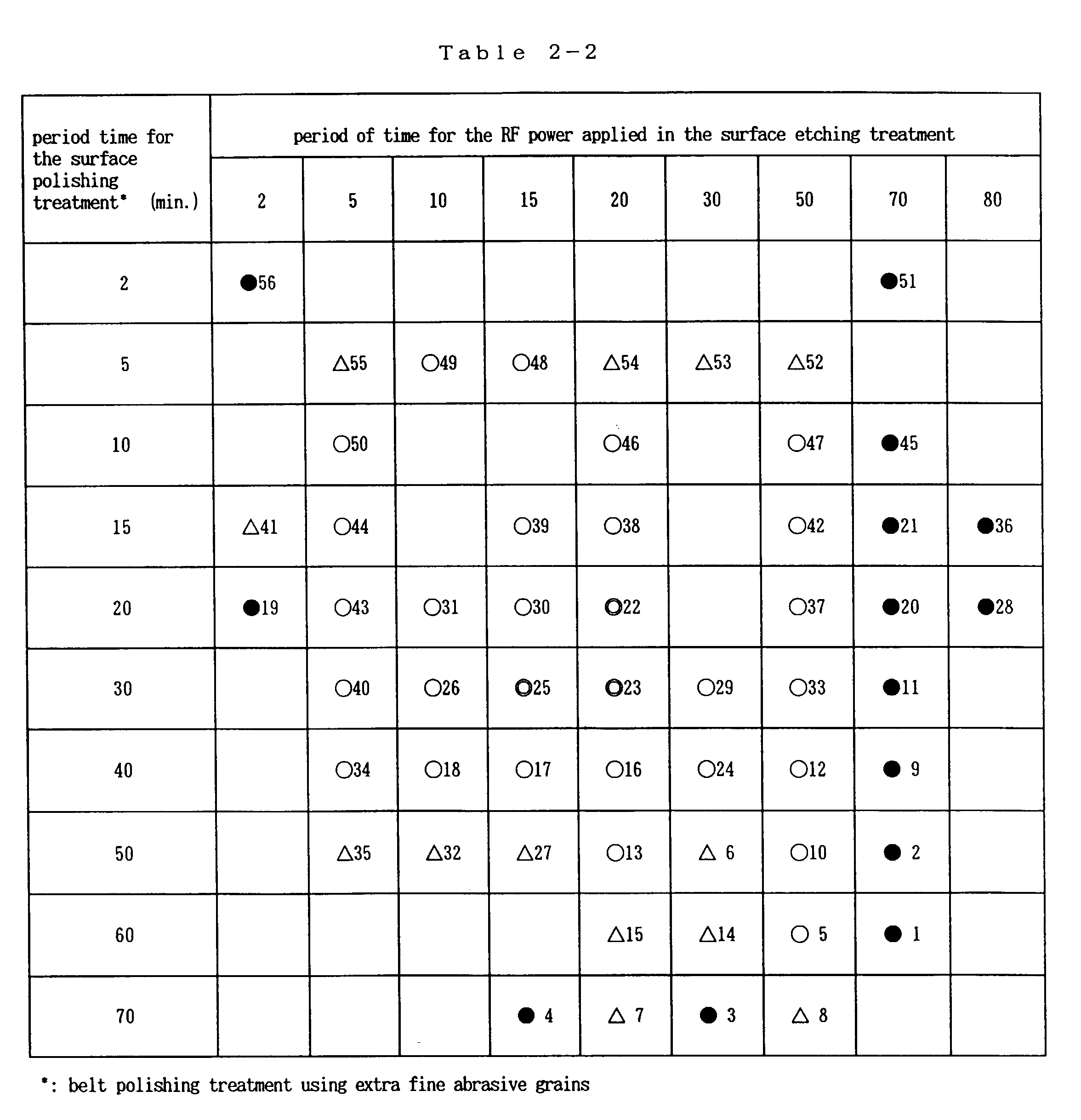


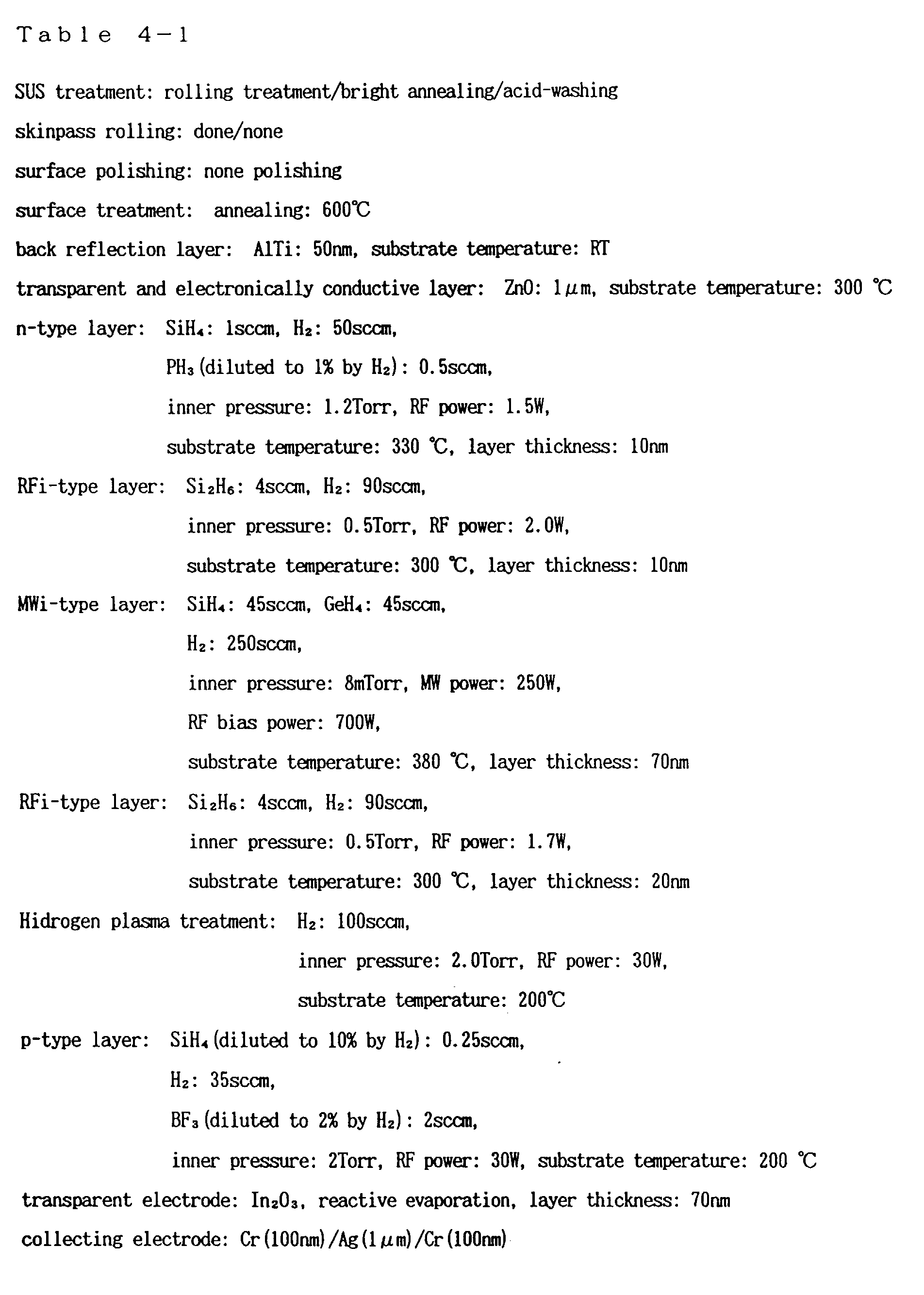


Claims (21)
- A photovoltaic device comprising an opaque substrate having an irregular surface structure comprising a plurality of linear irregularities or recesses arranged therein and a photoelectric conversion layer formed on said irregular surface structure of said substrate.
- A photovoltaic device according to claim 1, wherein the plurality of linear irregularities or recesses are arranged in a linear form arrangement.
- A photovoltaic device according to claim 1, wherein the plurality of linear irregularities or recesses are arranged in a wave-like form arrangement.
- A photovoltaic device according to claim 1, wherein the plurality of linear irregularities or recesses are arranged in a spiral form arrangement.
- A photovoltaic device according to claim 1, wherein the plurality of linear irregularities or recesses have a center line average roughness Ra(X) of 15 nm to 300 nm when scanned in a direction parallel to the linear irregularities or recesses, a center line average roughness Ra(Y) of 20 nm to 600 nm when scanned in a direction perpendicular to the linear irregularities or recesses, and a Ra(X)/Ra(Y) ratio of 0.8 or less.
- A photovoltaic device according to claim 2, wherein the plurality of linear irregularities or recesses have a pitch in the range of 0.5 to 20 µm.
- A photovoltaic device according to claim 1, wherein the irregular surface structure comprises a plurality of first linear irregularities or recesses arranged in a linear form arrangement and a plurality of second linear irregularities or recesses arranged in a direction perpendicular to said first linear irregularities or recesses.
- A photovoltaic device according to claim 7, wherein the second linear irregularities or recesses are of 20 um or less in length.
- A photovoltaic device according to any preceding claim, wherein the opaque substrate is composed of a metallic material or an alloy material.
- A photovoltaic device according to any preceding claim, wherein the opaque substrate has flexibility.
- A photovoltaic device according to any preceding claim which further comprises a back reflection layer interposed between the opaque substrate and the photoelectric conversion layer.
- A photovoltaic device according to claim 11, wherein the back reflection layer contains at least an element selected from the group consisting of Au, Ag, Cu, Al and Mg.
- A photovoltaic device according to claim 12, wherein the back reflection layer further contains Si.
- A photovoltaic device according to claim 11, wherein the back reflection layer has a multi-layered structure.
- A photovoltaic device according to claim 12 which further comprises a transparent and electrically conductive layer interposed between the back reflection layer and the photoelectric conversion layer.
- A photovoltaic device according to claim 15, wherein the transparent and electrically conductive layer comprises a zinc oxide.
- A photovoltaic device according to any preceding claim, wherein the photoelectric conversion layer has an irregular surface structure comprising a plurality of linear irregularities or recesses arranged therein.
- A photovoltaic device according to any preceding claim, wherein the photoelectric conversion layer has a multi-layered structure.
- A photovoltaic device according to any preceding claim, wherein the photoelectric conversion layer comprises a non-single crystalline semiconductor material.
- A photovoltaic device according to claim 1, wherein the opaque substrate has a long length.
- A photovoltaic device according to claim 20, wherein the opaque substrate is of belt-like long web form.
Applications Claiming Priority (3)
| Application Number | Priority Date | Filing Date | Title |
|---|---|---|---|
| JP3985696 | 1996-02-27 | ||
| JP39856/96 | 1996-02-27 | ||
| JP3985696 | 1996-02-27 |
Publications (3)
| Publication Number | Publication Date |
|---|---|
| EP0793277A2 true EP0793277A2 (en) | 1997-09-03 |
| EP0793277A3 EP0793277A3 (en) | 1998-09-09 |
| EP0793277B1 EP0793277B1 (en) | 2001-08-22 |
Family
ID=12564624
Family Applications (1)
| Application Number | Title | Priority Date | Filing Date |
|---|---|---|---|
| EP97301265A Expired - Lifetime EP0793277B1 (en) | 1996-02-27 | 1997-02-26 | Photovoltaic device provided with an opaque substrate having a specific irregular surface structure |
Country Status (5)
| Country | Link |
|---|---|
| US (1) | US6072117A (en) |
| EP (1) | EP0793277B1 (en) |
| KR (1) | KR100267515B1 (en) |
| CN (1) | CN1096713C (en) |
| DE (1) | DE69708463T2 (en) |
Cited By (14)
| Publication number | Priority date | Publication date | Assignee | Title |
|---|---|---|---|---|
| WO2001022500A1 (en) * | 1999-09-17 | 2001-03-29 | Pacific Solar Pty. Limited | Recrystallisation of semiconductor material |
| EP1100130A1 (en) * | 1998-06-01 | 2001-05-16 | Kaneka Corporation | Silicon-base thin-film photoelectric device |
| WO2003007386A1 (en) * | 2001-07-13 | 2003-01-23 | Midwest Research Institute | Thin-film solar cell fabricated on a flexible metallic substrate |
| US6593522B2 (en) * | 2000-03-29 | 2003-07-15 | Sanyo Electric Co., Ltd. | Solar cell device |
| EP1416541A2 (en) * | 2002-10-04 | 2004-05-06 | Sumitomo Metal Mining Co., Ltd. | Transparent oxide electrode film and manufacturing method thereof, transparent electroconductive base Material, solar cell and photo detection element |
| US7053294B2 (en) | 2001-07-13 | 2006-05-30 | Midwest Research Institute | Thin-film solar cell fabricated on a flexible metallic substrate |
| US7306823B2 (en) | 2004-09-18 | 2007-12-11 | Nanosolar, Inc. | Coated nanoparticles and quantum dots for solution-based fabrication of photovoltaic cells |
| US7700464B2 (en) | 2004-02-19 | 2010-04-20 | Nanosolar, Inc. | High-throughput printing of semiconductor precursor layer from nanoflake particles |
| US7732229B2 (en) | 2004-09-18 | 2010-06-08 | Nanosolar, Inc. | Formation of solar cells with conductive barrier layers and foil substrates |
| US8541048B1 (en) | 2004-09-18 | 2013-09-24 | Nanosolar, Inc. | Formation of photovoltaic absorber layers on foil substrates |
| US8642455B2 (en) | 2004-02-19 | 2014-02-04 | Matthew R. Robinson | High-throughput printing of semiconductor precursor layer from nanoflake particles |
| CN104334752A (en) * | 2012-05-23 | 2015-02-04 | 杰富意钢铁株式会社 | Stainless steel foil solar cell substrate material and method for manufacturing same |
| WO2018116245A1 (en) * | 2016-12-23 | 2018-06-28 | Sabic Global Technologies B.V. | Electrically-conductive copolyestercarbonate-based material |
| US20210098528A1 (en) * | 2010-10-18 | 2021-04-01 | Wake Forest University | Thermoelectric Apparatus And Applications Thereof |
Families Citing this family (70)
| Publication number | Priority date | Publication date | Assignee | Title |
|---|---|---|---|---|
| JP3719632B2 (en) * | 1998-12-17 | 2005-11-24 | 三菱電機株式会社 | Method for manufacturing silicon solar cell |
| US6787692B2 (en) | 2000-10-31 | 2004-09-07 | National Institute Of Advanced Industrial Science & Technology | Solar cell substrate, thin-film solar cell, and multi-junction thin-film solar cell |
| US6750394B2 (en) * | 2001-01-12 | 2004-06-15 | Sharp Kabushiki Kaisha | Thin-film solar cell and its manufacturing method |
| US6761986B2 (en) * | 2001-04-06 | 2004-07-13 | Rockwell Scientific Licensing, Llc | Thin film infrared transparent conductor |
| US6788721B2 (en) * | 2001-04-27 | 2004-09-07 | Sarnoff Corporation | Photonic integrated circuit (PIC) and method for making same |
| US7442629B2 (en) | 2004-09-24 | 2008-10-28 | President & Fellows Of Harvard College | Femtosecond laser-induced formation of submicrometer spikes on a semiconductor substrate |
| US7057256B2 (en) | 2001-05-25 | 2006-06-06 | President & Fellows Of Harvard College | Silicon-based visible and near-infrared optoelectric devices |
| WO2003036657A1 (en) * | 2001-10-19 | 2003-05-01 | Asahi Glass Company, Limited | Substrate with transparent conductive oxide film and production method therefor, and photoelectric conversion element |
| EP1462540B1 (en) * | 2001-12-03 | 2012-03-07 | Nippon Sheet Glass Company, Limited | Method for forming thin film. |
| DE10392353B4 (en) * | 2002-03-06 | 2008-09-25 | Sharp K.K. | A method of manufacturing a solar cell, the emitter semiconductor layer of which gradually becomes thinner as the distance from front electrodes increases |
| US7995871B2 (en) * | 2002-05-07 | 2011-08-09 | Nanoptek Corporation | Stress-induced bandgap-shifted semiconductor photoelectrolytic/photocatalytic/photovoltaic surface and method for making same |
| US8673399B2 (en) * | 2002-05-07 | 2014-03-18 | Nanoptek Corporation | Bandgap-shifted semiconductor surface and method for making same, and apparatus for using same |
| US7485799B2 (en) * | 2002-05-07 | 2009-02-03 | John Michael Guerra | Stress-induced bandgap-shifted semiconductor photoelectrolytic/photocatalytic/photovoltaic surface and method for making same |
| US20080283121A1 (en) * | 2002-05-07 | 2008-11-20 | Nanoptek Corporation | Bandgap-shifted semiconductor surface and method for making same, and apparatus for using same |
| JP2004356623A (en) * | 2003-05-08 | 2004-12-16 | Canon Inc | Laminated photovoltaic element and method of manufacture the same |
| JP2005005639A (en) * | 2003-06-16 | 2005-01-06 | Canon Inc | Method and device for measuring photoelectric transfer characteristic of solar cell element |
| JP2005032852A (en) * | 2003-07-09 | 2005-02-03 | Matsushita Electric Ind Co Ltd | Organic photoelectric conversion device |
| EP1513171A1 (en) * | 2003-09-05 | 2005-03-09 | Sony International (Europe) GmbH | Tandem dye-sensitised solar cell and method of its production |
| US8846141B1 (en) | 2004-02-19 | 2014-09-30 | Aeris Capital Sustainable Ip Ltd. | High-throughput printing of semiconductor precursor layer from microflake particles |
| US20090032108A1 (en) * | 2007-03-30 | 2009-02-05 | Craig Leidholm | Formation of photovoltaic absorber layers on foil substrates |
| US8927315B1 (en) | 2005-01-20 | 2015-01-06 | Aeris Capital Sustainable Ip Ltd. | High-throughput assembly of series interconnected solar cells |
| US8816191B2 (en) * | 2005-11-29 | 2014-08-26 | Banpil Photonics, Inc. | High efficiency photovoltaic cells and manufacturing thereof |
| US20080178932A1 (en) * | 2006-11-02 | 2008-07-31 | Guardian Industries Corp. | Front electrode including transparent conductive coating on patterned glass substrate for use in photovoltaic device and method of making same |
| JP5442453B2 (en) * | 2007-02-15 | 2014-03-12 | マサチューセッツ インスティテュート オブ テクノロジー | Solar cell with uneven surface |
| ATE504086T1 (en) * | 2007-05-28 | 2011-04-15 | Consiglio Nazionale Ricerche | PHOTOVOLTAIC DEVICE WITH IMPROVED LIGHT COLLECTION |
| US7875945B2 (en) * | 2007-06-12 | 2011-01-25 | Guardian Industries Corp. | Rear electrode structure for use in photovoltaic device such as CIGS/CIS photovoltaic device and method of making same |
| US20080308147A1 (en) * | 2007-06-12 | 2008-12-18 | Yiwei Lu | Rear electrode structure for use in photovoltaic device such as CIGS/CIS photovoltaic device and method of making same |
| US7846750B2 (en) * | 2007-06-12 | 2010-12-07 | Guardian Industries Corp. | Textured rear electrode structure for use in photovoltaic device such as CIGS/CIS solar cell |
| CN101355109A (en) * | 2007-07-26 | 2009-01-28 | 鸿富锦精密工业(深圳)有限公司 | Solar battery component and manufacturing equipment thereof |
| CN101359698A (en) * | 2007-08-01 | 2009-02-04 | 鸿富锦精密工业(深圳)有限公司 | Solar cell, manufacturing apparatus and manufacturing method thereof |
| CN101363266A (en) * | 2007-08-09 | 2009-02-11 | 鸿富锦精密工业(深圳)有限公司 | Solar house |
| CN101363267A (en) * | 2007-08-10 | 2009-02-11 | 鸿富锦精密工业(深圳)有限公司 | Solar roof and solar house |
| JP4418500B2 (en) * | 2008-03-28 | 2010-02-17 | 三菱重工業株式会社 | Photoelectric conversion device and manufacturing method thereof |
| CN101807615B (en) * | 2009-02-18 | 2012-05-30 | 晶元光电股份有限公司 | Photovoltaic device with light collecting effect electrode structure |
| TWI379430B (en) * | 2009-04-16 | 2012-12-11 | Atomic Energy Council | A method of fabricating a thin interface for internal light reflection and impurities isolation |
| TW201112439A (en) * | 2009-06-22 | 2011-04-01 | First Solar Inc | Method and apparatus for annealing a deposited cadmium stannate layer |
| WO2011005319A1 (en) * | 2009-07-09 | 2011-01-13 | Xunlight Corporation | Back reflector for photovoltaic devices |
| US20120147286A1 (en) * | 2009-08-19 | 2012-06-14 | Sharp Kabushiki Kaisha | Photosensor, semiconductor device, and liquid crystal panel |
| WO2011021477A1 (en) * | 2009-08-20 | 2011-02-24 | シャープ株式会社 | Optical sensor, semiconductor device, and liquid crystal panel |
| US20110048518A1 (en) * | 2009-08-26 | 2011-03-03 | Molecular Imprints, Inc. | Nanostructured thin film inorganic solar cells |
| US9911781B2 (en) | 2009-09-17 | 2018-03-06 | Sionyx, Llc | Photosensitive imaging devices and associated methods |
| US9673243B2 (en) | 2009-09-17 | 2017-06-06 | Sionyx, Llc | Photosensitive imaging devices and associated methods |
| US8895844B2 (en) * | 2009-10-23 | 2014-11-25 | The Board Of Trustees Of The Leland Stanford Junior University | Solar cell comprising a plasmonic back reflector and method therefor |
| US8896077B2 (en) * | 2009-10-23 | 2014-11-25 | The Board Of Trustees Of The Leland Stanford Junior University | Optoelectronic semiconductor device and method of fabrication |
| US20110120536A1 (en) * | 2009-11-20 | 2011-05-26 | Dapeng Wang | Roughness control of a wavelength selective reflector layer for thin film solar applications |
| JP2011114004A (en) * | 2009-11-24 | 2011-06-09 | Panasonic Electric Works Co Ltd | Organic solar cell |
| US8212250B2 (en) | 2009-12-10 | 2012-07-03 | Leonard Forbes | Backside texturing by cusps to improve IR response of silicon solar cells and photodetectors |
| US8120027B2 (en) * | 2009-12-10 | 2012-02-21 | Leonard Forbes | Backside nanoscale texturing to improve IR response of silicon solar cells and photodetectors |
| US8999857B2 (en) | 2010-04-02 | 2015-04-07 | The Board Of Trustees Of The Leland Stanford Junior University | Method for forming a nano-textured substrate |
| US8692198B2 (en) | 2010-04-21 | 2014-04-08 | Sionyx, Inc. | Photosensitive imaging devices and associated methods |
| CN106449684B (en) | 2010-06-18 | 2019-09-27 | 西奥尼克斯公司 | High speed photosensitive device and correlation technique |
| US8404302B2 (en) * | 2010-07-14 | 2013-03-26 | Sharp Laboratories Of America, Inc. | Solution process for fabricating a textured transparent conductive oxide (TCO) |
| US8476105B2 (en) * | 2010-12-22 | 2013-07-02 | General Electric Company | Method of making a transparent conductive oxide layer and a photovoltaic device |
| JP5884077B2 (en) * | 2010-12-29 | 2016-03-15 | パナソニックIpマネジメント株式会社 | Solar cell and solar cell module |
| US8859321B2 (en) * | 2011-01-31 | 2014-10-14 | International Business Machines Corporation | Mixed temperature deposition of thin film silicon tandem cells |
| KR101269608B1 (en) * | 2011-03-29 | 2013-06-05 | 한국에너지기술연구원 | Back reflection layer for thin film solar cell, fabrication method of the same and thin film solar cell comprising the same |
| US9496308B2 (en) | 2011-06-09 | 2016-11-15 | Sionyx, Llc | Process module for increasing the response of backside illuminated photosensitive imagers and associated methods |
| EP2732402A2 (en) | 2011-07-13 | 2014-05-21 | Sionyx, Inc. | Biometric imaging devices and associated methods |
| JPWO2013015173A1 (en) * | 2011-07-25 | 2015-02-23 | 日立化成株式会社 | Solar cell substrate, method for manufacturing solar cell substrate, solar cell element, and solar cell |
| US9064764B2 (en) | 2012-03-22 | 2015-06-23 | Sionyx, Inc. | Pixel isolation elements, devices, and associated methods |
| US10319872B2 (en) * | 2012-05-10 | 2019-06-11 | International Business Machines Corporation | Cost-efficient high power PECVD deposition for solar cells |
| KR20150130303A (en) | 2013-02-15 | 2015-11-23 | 사이오닉스, 아이엔씨. | High dynamic range cmos image sensor having anti-blooming properties and associated methods |
| WO2014151093A1 (en) | 2013-03-15 | 2014-09-25 | Sionyx, Inc. | Three dimensional imaging utilizing stacked imager devices and associated methods |
| US9209345B2 (en) | 2013-06-29 | 2015-12-08 | Sionyx, Inc. | Shallow trench textured regions and associated methods |
| US10840400B2 (en) * | 2013-08-29 | 2020-11-17 | Taiwan Semiconductor Manufacturing Co., Ltd. | Photovoltaic device with back reflector |
| US9548419B2 (en) | 2014-05-20 | 2017-01-17 | Southern Taiwan University Of Science And Technology | Light emitting diode chip having multi microstructure substrate surface |
| JP6513788B2 (en) * | 2015-03-24 | 2019-05-15 | 株式会社カネカ | Method of manufacturing crystalline silicon solar cell and method of manufacturing crystalline silicon solar cell module |
| EP3095882B1 (en) | 2015-05-18 | 2021-09-22 | Outokumpu Oyj | Method for producing a stainless steel sheet with modified visual characteristics |
| CN107104171B (en) * | 2017-05-17 | 2019-06-04 | 常州大学 | A kind of preparation method of micro nano structure bismuth ferrite photovoltaic device |
| CN108346674B (en) * | 2018-01-30 | 2019-01-18 | 武汉新芯集成电路制造有限公司 | Preparation method, silicon wafer and the imaging sensor of semiconductor wafers |
Citations (4)
| Publication number | Priority date | Publication date | Assignee | Title |
|---|---|---|---|---|
| US4377723A (en) * | 1980-05-02 | 1983-03-22 | The University Of Delaware | High efficiency thin-film multiple-gap photovoltaic device |
| EP0107357A2 (en) * | 1982-09-24 | 1984-05-02 | Energy Conversion Devices, Inc. | Apparatus and method for making large area photovoltaic devices incorporating back reflectors |
| US4493942A (en) * | 1983-01-18 | 1985-01-15 | Exxon Research And Engineering Co. | Solar cell with two-dimensional reflecting diffraction grating |
| EP0661761A2 (en) * | 1993-12-30 | 1995-07-05 | Canon Kabushiki Kaisha | Method of manufacturing photoelectric transducer |
Family Cites Families (9)
| Publication number | Priority date | Publication date | Assignee | Title |
|---|---|---|---|---|
| US4571448A (en) * | 1981-11-16 | 1986-02-18 | University Of Delaware | Thin film photovoltaic solar cell and method of making the same |
| JPS594310A (en) * | 1982-06-30 | 1984-01-11 | Toshiba Corp | Surface acoustic wave device |
| JPS59152676A (en) * | 1983-02-21 | 1984-08-31 | Sumitomo Electric Ind Ltd | Amorphous silicon photovoltaic element |
| US4532372A (en) * | 1983-12-23 | 1985-07-30 | Energy Conversion Devices, Inc. | Barrier layer for photovoltaic devices |
| US4598306A (en) * | 1983-07-28 | 1986-07-01 | Energy Conversion Devices, Inc. | Barrier layer for photovoltaic devices |
| JPS604187A (en) * | 1983-06-20 | 1985-01-10 | Taiho Yakuhin Kogyo Kk | Pyrazole compound |
| IN165761B (en) * | 1983-07-28 | 1990-01-06 | Energy Conversion Devices Inc | |
| JPS6214788A (en) * | 1985-07-12 | 1987-01-23 | Res Assoc Util Of Light Oil | Production of methacrylic acid |
| JPH03205879A (en) * | 1990-01-08 | 1991-09-09 | Hitachi Ltd | Solar cell |
-
1997
- 1997-02-26 DE DE69708463T patent/DE69708463T2/en not_active Expired - Lifetime
- 1997-02-26 EP EP97301265A patent/EP0793277B1/en not_active Expired - Lifetime
- 1997-02-26 US US08/806,315 patent/US6072117A/en not_active Expired - Lifetime
- 1997-02-27 KR KR1019970006324A patent/KR100267515B1/en not_active IP Right Cessation
- 1997-02-27 CN CN97109999A patent/CN1096713C/en not_active Expired - Fee Related
Patent Citations (4)
| Publication number | Priority date | Publication date | Assignee | Title |
|---|---|---|---|---|
| US4377723A (en) * | 1980-05-02 | 1983-03-22 | The University Of Delaware | High efficiency thin-film multiple-gap photovoltaic device |
| EP0107357A2 (en) * | 1982-09-24 | 1984-05-02 | Energy Conversion Devices, Inc. | Apparatus and method for making large area photovoltaic devices incorporating back reflectors |
| US4493942A (en) * | 1983-01-18 | 1985-01-15 | Exxon Research And Engineering Co. | Solar cell with two-dimensional reflecting diffraction grating |
| EP0661761A2 (en) * | 1993-12-30 | 1995-07-05 | Canon Kabushiki Kaisha | Method of manufacturing photoelectric transducer |
Non-Patent Citations (1)
| Title |
|---|
| PATENT ABSTRACTS OF JAPAN vol. 008, no. 285 (E-287), 26 December 1984 & JP 59 152676 A (SUMITOMO DENKI KOGYO KK), 31 August 1984, * |
Cited By (23)
| Publication number | Priority date | Publication date | Assignee | Title |
|---|---|---|---|---|
| EP1100130A1 (en) * | 1998-06-01 | 2001-05-16 | Kaneka Corporation | Silicon-base thin-film photoelectric device |
| EP1100130A4 (en) * | 1998-06-01 | 2001-11-28 | Kaneka Corp | Silicon-base thin-film photoelectric device |
| WO2001022500A1 (en) * | 1999-09-17 | 2001-03-29 | Pacific Solar Pty. Limited | Recrystallisation of semiconductor material |
| US6593522B2 (en) * | 2000-03-29 | 2003-07-15 | Sanyo Electric Co., Ltd. | Solar cell device |
| US7053294B2 (en) | 2001-07-13 | 2006-05-30 | Midwest Research Institute | Thin-film solar cell fabricated on a flexible metallic substrate |
| WO2003007386A1 (en) * | 2001-07-13 | 2003-01-23 | Midwest Research Institute | Thin-film solar cell fabricated on a flexible metallic substrate |
| US7507357B2 (en) | 2002-10-04 | 2009-03-24 | Sumitomo Metal Mining Co., Ltd. | Transparent oxide electrode film and manufacturing method thereof, transparent electroconductive base material, solar cell and photo detection element |
| EP1416541A3 (en) * | 2002-10-04 | 2006-05-03 | Sumitomo Metal Mining Co., Ltd. | Transparent oxide electrode film and manufacturing method thereof, transparent electroconductive base Material, solar cell and photo detection element |
| EP1981089A3 (en) * | 2002-10-04 | 2008-10-22 | Sumitomo Metal Mining Co., Ltd. | Transparent electrode film based on indium oxide with titanium and tungsten admixtures and manufacturing method thereof |
| EP1416541A2 (en) * | 2002-10-04 | 2004-05-06 | Sumitomo Metal Mining Co., Ltd. | Transparent oxide electrode film and manufacturing method thereof, transparent electroconductive base Material, solar cell and photo detection element |
| US7575698B2 (en) | 2002-10-04 | 2009-08-18 | Sumitomo Metal Mining Co., Ltd. | TI and W containing transparent oxide electrode film |
| US8642455B2 (en) | 2004-02-19 | 2014-02-04 | Matthew R. Robinson | High-throughput printing of semiconductor precursor layer from nanoflake particles |
| US7700464B2 (en) | 2004-02-19 | 2010-04-20 | Nanosolar, Inc. | High-throughput printing of semiconductor precursor layer from nanoflake particles |
| US8541048B1 (en) | 2004-09-18 | 2013-09-24 | Nanosolar, Inc. | Formation of photovoltaic absorber layers on foil substrates |
| US8193442B2 (en) | 2004-09-18 | 2012-06-05 | Nanosolar, Inc. | Coated nanoparticles and quantum dots for solution-based fabrication of photovoltaic cells |
| US7732229B2 (en) | 2004-09-18 | 2010-06-08 | Nanosolar, Inc. | Formation of solar cells with conductive barrier layers and foil substrates |
| US7306823B2 (en) | 2004-09-18 | 2007-12-11 | Nanosolar, Inc. | Coated nanoparticles and quantum dots for solution-based fabrication of photovoltaic cells |
| US8809678B2 (en) | 2004-09-18 | 2014-08-19 | Aeris Capital Sustainable Ip Ltd. | Coated nanoparticles and quantum dots for solution-based fabrication of photovoltaic cells |
| US20210098528A1 (en) * | 2010-10-18 | 2021-04-01 | Wake Forest University | Thermoelectric Apparatus And Applications Thereof |
| CN104334752A (en) * | 2012-05-23 | 2015-02-04 | 杰富意钢铁株式会社 | Stainless steel foil solar cell substrate material and method for manufacturing same |
| CN104334752B (en) * | 2012-05-23 | 2016-11-09 | 杰富意钢铁株式会社 | Stainless steel foil solar cell substrate material and manufacture method thereof |
| WO2018116245A1 (en) * | 2016-12-23 | 2018-06-28 | Sabic Global Technologies B.V. | Electrically-conductive copolyestercarbonate-based material |
| KR20190087660A (en) * | 2016-12-23 | 2019-07-24 | 사빅 글로벌 테크놀러지스 비.브이. | Electrically conductive copolyester carbonate-based materials |
Also Published As
| Publication number | Publication date |
|---|---|
| DE69708463D1 (en) | 2001-12-20 |
| US6072117A (en) | 2000-06-06 |
| CN1096713C (en) | 2002-12-18 |
| EP0793277B1 (en) | 2001-08-22 |
| EP0793277A3 (en) | 1998-09-09 |
| KR100267515B1 (en) | 2000-10-16 |
| CN1174415A (en) | 1998-02-25 |
| DE69708463T2 (en) | 2002-05-16 |
| KR970063769A (en) | 1997-09-12 |
Similar Documents
| Publication | Publication Date | Title |
|---|---|---|
| EP0793277B1 (en) | Photovoltaic device provided with an opaque substrate having a specific irregular surface structure | |
| US6331672B1 (en) | Photovoltaic cell and method for manufacturing the same | |
| EP0895291B1 (en) | Photovoltaic element and method of producing the same | |
| US6106689A (en) | Process for forming zinc oxide film and processes for producing semiconductor device substrate and photo-electricity generating device using the film | |
| US6184456B1 (en) | Photovoltaic device | |
| JP2771414B2 (en) | Solar cell manufacturing method | |
| JP2829653B2 (en) | Photovoltaic element | |
| US6812499B2 (en) | Silicon-based film and photovoltaic element | |
| JP2004311965A (en) | Fabrication method of photovoltaic device | |
| Takano et al. | Light-weight and large-area solar cell production technology | |
| US5897332A (en) | Method for manufacturing photoelectric conversion element | |
| JP3787410B2 (en) | Deposited film manufacturing method and photovoltaic device manufacturing method | |
| JPH08298333A (en) | Semiconductor coating film forming equipment, and thin film solar cell and forming method of thin film solar cell | |
| JPH11195801A (en) | Photovoltaic element | |
| JP4416569B2 (en) | Deposited film forming method and deposited film forming apparatus | |
| JP2846508B2 (en) | Photovoltaic element | |
| JPH10209479A (en) | Manufacturing apparatus of semiconductor thin film and photovoltaic device | |
| JPH09293892A (en) | Photovoltaic element | |
| JP3072831B2 (en) | Photovoltaic element | |
| JP3445132B2 (en) | Method for manufacturing zinc oxide thin film, method for manufacturing semiconductor element substrate using the same, method for manufacturing photoelectric conversion element, zinc oxide thin film, semiconductor element substrate, and photoelectric conversion element | |
| AU756834B2 (en) | Method of producing a microcrystal semiconductor thin film | |
| JPH10173216A (en) | Photovoltaic element | |
| JPH11274540A (en) | Photovoltaic element and manufacture thereof | |
| JPH10173211A (en) | Photovoltaic element | |
| JPH10200146A (en) | Photovoltaic element |
Legal Events
| Date | Code | Title | Description |
|---|---|---|---|
| PUAI | Public reference made under article 153(3) epc to a published international application that has entered the european phase |
Free format text: ORIGINAL CODE: 0009012 |
|
| 17P | Request for examination filed |
Effective date: 19970312 |
|
| AK | Designated contracting states |
Kind code of ref document: A2 Designated state(s): CH DE FR GB IT LI |
|
| PUAL | Search report despatched |
Free format text: ORIGINAL CODE: 0009013 |
|
| AK | Designated contracting states |
Kind code of ref document: A3 Designated state(s): CH DE FR GB IT LI |
|
| 17Q | First examination report despatched |
Effective date: 19980902 |
|
| GRAG | Despatch of communication of intention to grant |
Free format text: ORIGINAL CODE: EPIDOS AGRA |
|
| GRAG | Despatch of communication of intention to grant |
Free format text: ORIGINAL CODE: EPIDOS AGRA |
|
| 17Q | First examination report despatched |
Effective date: 19980902 |
|
| 18R | Application refused |
Effective date: 20000124 |
|
| GRAG | Despatch of communication of intention to grant |
Free format text: ORIGINAL CODE: EPIDOS AGRA |
|
| GRAH | Despatch of communication of intention to grant a patent |
Free format text: ORIGINAL CODE: EPIDOS IGRA |
|
| D18R | Application refused (deleted) | ||
| GRAH | Despatch of communication of intention to grant a patent |
Free format text: ORIGINAL CODE: EPIDOS IGRA |
|
| GRAA | (expected) grant |
Free format text: ORIGINAL CODE: 0009210 |
|
| ITF | It: translation for a ep patent filed |
Owner name: SOCIETA' ITALIANA BREVETTI S.P.A. |
|
| AK | Designated contracting states |
Kind code of ref document: B1 Designated state(s): CH DE FR GB IT LI |
|
| REG | Reference to a national code |
Ref country code: CH Ref legal event code: NV Representative=s name: BOVARD AG PATENTANWAELTE Ref country code: CH Ref legal event code: EP |
|
| ET | Fr: translation filed | ||
| REF | Corresponds to: |
Ref document number: 69708463 Country of ref document: DE Date of ref document: 20011220 |
|
| REG | Reference to a national code |
Ref country code: GB Ref legal event code: IF02 |
|
| PLBE | No opposition filed within time limit |
Free format text: ORIGINAL CODE: 0009261 |
|
| STAA | Information on the status of an ep patent application or granted ep patent |
Free format text: STATUS: NO OPPOSITION FILED WITHIN TIME LIMIT |
|
| 26N | No opposition filed | ||
| REG | Reference to a national code |
Ref country code: CH Ref legal event code: PFA Owner name: CANON KABUSHIKI KAISHA Free format text: CANON KABUSHIKI KAISHA#30-2, 3-CHOME, SHIMOMARUKO, OHTA-KU#TOKYO (JP) -TRANSFER TO- CANON KABUSHIKI KAISHA#30-2, 3-CHOME, SHIMOMARUKO, OHTA-KU#TOKYO (JP) |
|
| PGFP | Annual fee paid to national office [announced via postgrant information from national office to epo] |
Ref country code: DE Payment date: 20140228 Year of fee payment: 18 Ref country code: CH Payment date: 20140221 Year of fee payment: 18 |
|
| PGFP | Annual fee paid to national office [announced via postgrant information from national office to epo] |
Ref country code: IT Payment date: 20140204 Year of fee payment: 18 Ref country code: FR Payment date: 20140228 Year of fee payment: 18 |
|
| PGFP | Annual fee paid to national office [announced via postgrant information from national office to epo] |
Ref country code: GB Payment date: 20140220 Year of fee payment: 18 |
|
| REG | Reference to a national code |
Ref country code: DE Ref legal event code: R119 Ref document number: 69708463 Country of ref document: DE |
|
| REG | Reference to a national code |
Ref country code: CH Ref legal event code: PL |
|
| GBPC | Gb: european patent ceased through non-payment of renewal fee |
Effective date: 20150226 |
|
| PG25 | Lapsed in a contracting state [announced via postgrant information from national office to epo] |
Ref country code: LI Free format text: LAPSE BECAUSE OF NON-PAYMENT OF DUE FEES Effective date: 20150228 Ref country code: CH Free format text: LAPSE BECAUSE OF NON-PAYMENT OF DUE FEES Effective date: 20150228 |
|
| REG | Reference to a national code |
Ref country code: FR Ref legal event code: ST Effective date: 20151030 |
|
| PG25 | Lapsed in a contracting state [announced via postgrant information from national office to epo] |
Ref country code: IT Free format text: LAPSE BECAUSE OF NON-PAYMENT OF DUE FEES Effective date: 20150226 |
|
| PG25 | Lapsed in a contracting state [announced via postgrant information from national office to epo] |
Ref country code: DE Free format text: LAPSE BECAUSE OF NON-PAYMENT OF DUE FEES Effective date: 20150901 Ref country code: GB Free format text: LAPSE BECAUSE OF NON-PAYMENT OF DUE FEES Effective date: 20150226 |
|
| PG25 | Lapsed in a contracting state [announced via postgrant information from national office to epo] |
Ref country code: FR Free format text: LAPSE BECAUSE OF NON-PAYMENT OF DUE FEES Effective date: 20150302 |